EP2006910A2 - Leistungselektronikmodul - Google Patents
Leistungselektronikmodul Download PDFInfo
- Publication number
- EP2006910A2 EP2006910A2 EP08104205A EP08104205A EP2006910A2 EP 2006910 A2 EP2006910 A2 EP 2006910A2 EP 08104205 A EP08104205 A EP 08104205A EP 08104205 A EP08104205 A EP 08104205A EP 2006910 A2 EP2006910 A2 EP 2006910A2
- Authority
- EP
- European Patent Office
- Prior art keywords
- substrate
- electronics module
- plastic carrier
- carrier substrate
- power
- Prior art date
- Legal status (The legal status is an assumption and is not a legal conclusion. Google has not performed a legal analysis and makes no representation as to the accuracy of the status listed.)
- Granted
Links
Images


Classifications
-
- H—ELECTRICITY
- H10—SEMICONDUCTOR DEVICES; ELECTRIC SOLID-STATE DEVICES NOT OTHERWISE PROVIDED FOR
- H10W—GENERIC PACKAGES, INTERCONNECTIONS, CONNECTORS OR OTHER CONSTRUCTIONAL DETAILS OF DEVICES COVERED BY CLASS H10
- H10W40/00—Arrangements for thermal protection or thermal control
- H10W40/10—Arrangements for heating
-
- H—ELECTRICITY
- H05—ELECTRIC TECHNIQUES NOT OTHERWISE PROVIDED FOR
- H05K—PRINTED CIRCUITS; CASINGS OR CONSTRUCTIONAL DETAILS OF ELECTRIC APPARATUS; MANUFACTURE OF ASSEMBLAGES OF ELECTRICAL COMPONENTS
- H05K3/00—Apparatus or processes for manufacturing printed circuits
- H05K3/0058—Laminating printed circuit boards onto other substrates, e.g. metallic substrates
-
- H—ELECTRICITY
- H10—SEMICONDUCTOR DEVICES; ELECTRIC SOLID-STATE DEVICES NOT OTHERWISE PROVIDED FOR
- H10W—GENERIC PACKAGES, INTERCONNECTIONS, CONNECTORS OR OTHER CONSTRUCTIONAL DETAILS OF DEVICES COVERED BY CLASS H10
- H10W40/00—Arrangements for thermal protection or thermal control
- H10W40/20—Arrangements for cooling
- H10W40/25—Arrangements for cooling characterised by their materials
-
- H—ELECTRICITY
- H10—SEMICONDUCTOR DEVICES; ELECTRIC SOLID-STATE DEVICES NOT OTHERWISE PROVIDED FOR
- H10W—GENERIC PACKAGES, INTERCONNECTIONS, CONNECTORS OR OTHER CONSTRUCTIONAL DETAILS OF DEVICES COVERED BY CLASS H10
- H10W70/00—Package substrates; Interposers; Redistribution layers [RDL]
- H10W70/60—Insulating or insulated package substrates; Interposers; Redistribution layers
- H10W70/611—Insulating or insulated package substrates; Interposers; Redistribution layers for connecting multiple chips together
-
- H—ELECTRICITY
- H10—SEMICONDUCTOR DEVICES; ELECTRIC SOLID-STATE DEVICES NOT OTHERWISE PROVIDED FOR
- H10W—GENERIC PACKAGES, INTERCONNECTIONS, CONNECTORS OR OTHER CONSTRUCTIONAL DETAILS OF DEVICES COVERED BY CLASS H10
- H10W70/00—Package substrates; Interposers; Redistribution layers [RDL]
- H10W70/60—Insulating or insulated package substrates; Interposers; Redistribution layers
- H10W70/67—Insulating or insulated package substrates; Interposers; Redistribution layers characterised by their insulating layers or insulating parts
- H10W70/688—Flexible insulating substrates
-
- H—ELECTRICITY
- H10—SEMICONDUCTOR DEVICES; ELECTRIC SOLID-STATE DEVICES NOT OTHERWISE PROVIDED FOR
- H10W—GENERIC PACKAGES, INTERCONNECTIONS, CONNECTORS OR OTHER CONSTRUCTIONAL DETAILS OF DEVICES COVERED BY CLASS H10
- H10W90/00—Package configurations
-
- H—ELECTRICITY
- H05—ELECTRIC TECHNIQUES NOT OTHERWISE PROVIDED FOR
- H05K—PRINTED CIRCUITS; CASINGS OR CONSTRUCTIONAL DETAILS OF ELECTRIC APPARATUS; MANUFACTURE OF ASSEMBLAGES OF ELECTRICAL COMPONENTS
- H05K1/00—Printed circuits
- H05K1/02—Details
- H05K1/0213—Electrical arrangements not otherwise provided for
- H05K1/0263—High current adaptations, e.g. printed high current conductors or using auxiliary non-printed means; Fine and coarse circuit patterns on one circuit board
-
- H—ELECTRICITY
- H05—ELECTRIC TECHNIQUES NOT OTHERWISE PROVIDED FOR
- H05K—PRINTED CIRCUITS; CASINGS OR CONSTRUCTIONAL DETAILS OF ELECTRIC APPARATUS; MANUFACTURE OF ASSEMBLAGES OF ELECTRICAL COMPONENTS
- H05K1/00—Printed circuits
- H05K1/18—Printed circuits structurally associated with non-printed electric components
- H05K1/189—Printed circuits structurally associated with non-printed electric components characterised by the use of flexible or folded printed circuits
-
- H—ELECTRICITY
- H05—ELECTRIC TECHNIQUES NOT OTHERWISE PROVIDED FOR
- H05K—PRINTED CIRCUITS; CASINGS OR CONSTRUCTIONAL DETAILS OF ELECTRIC APPARATUS; MANUFACTURE OF ASSEMBLAGES OF ELECTRICAL COMPONENTS
- H05K2201/00—Indexing scheme relating to printed circuits covered by H05K1/00
- H05K2201/03—Conductive materials
- H05K2201/032—Materials
- H05K2201/0323—Carbon
-
- H—ELECTRICITY
- H05—ELECTRIC TECHNIQUES NOT OTHERWISE PROVIDED FOR
- H05K—PRINTED CIRCUITS; CASINGS OR CONSTRUCTIONAL DETAILS OF ELECTRIC APPARATUS; MANUFACTURE OF ASSEMBLAGES OF ELECTRICAL COMPONENTS
- H05K2201/00—Indexing scheme relating to printed circuits covered by H05K1/00
- H05K2201/10—Details of components or other objects attached to or integrated in a printed circuit board
- H05K2201/10007—Types of components
- H05K2201/10166—Transistor
-
- H—ELECTRICITY
- H10—SEMICONDUCTOR DEVICES; ELECTRIC SOLID-STATE DEVICES NOT OTHERWISE PROVIDED FOR
- H10W—GENERIC PACKAGES, INTERCONNECTIONS, CONNECTORS OR OTHER CONSTRUCTIONAL DETAILS OF DEVICES COVERED BY CLASS H10
- H10W40/00—Arrangements for thermal protection or thermal control
- H10W40/20—Arrangements for cooling
- H10W40/25—Arrangements for cooling characterised by their materials
- H10W40/255—Arrangements for cooling characterised by their materials having a laminate or multilayered structure, e.g. direct bond copper [DBC] ceramic substrates
Definitions
- the invention relates to a power electronics module having at least one circuit carrier and at least one power semiconductor.
- thermally favorable circuit carriers are expensive to manufacture and a variety of soldering processes and / or Drahtbond revitalizing of the power semiconductors.
- the circuit carrier has a flexible plastic carrier substrate, in particular with copper conductor tracks, on which the power semiconductor is mounted, that the circuit carrier has a flexible Enticarmungssubstrat which is arranged flat on the plastic carrier substrate and that the circuit carrier has a flexible contacting substrate , which is arranged flat on the composite of plastic carrier substrate and Entracermungssubstrat component.
- a circuit carrier having a layer-like construction is provided, wherein the base is formed by the plastic carrier substrate, which is advantageously designed flexibly. On this the power semiconductor is mounted.
- the present circuit carrier is cheaper and easier to produce due to the use of the plastic carrier substrate.
- the Entracermungssubstrat serves for dissipating or spreading and distributing the heat from the power semiconductor or the circuit carrier. Finally, the heat is dissipated via copper on the plastic carrier substrate and the contacting substrate. It is also flexible and is arranged flat on the plastic carrier substrate, so that the Entracermungssubstrat the plastic carrier substrate advantageously substantially covers, more preferably the Entracermungssubstrat is slightly smaller, so that an edge region of the plastic carrier substrate is freely accessible. As a result, a simple contacting arranged on the plastic support substrate electrical contacts that lead from or to the power semiconductor, guaranteed.
- the plastic carrier substrate and the Entracermungssubstrat together form a component on which the contacting substrate is arranged flat.
- a flexible power electronics module is provided.
- the flexibility of the power electronics module is also dependent on further factors, such as the size and number of interconnects arranged on the circuit carrier and / or the dimensions and the number of power semiconductors. Due to the flexible design, the reliability of the power electronics module is increased in the long term because it can adapt to changing environmental conditions and shape and / or position tolerances, and on the other hand is ensured by the Entracermungssubstrat a particularly favorable cooling of the power electronics module.
- the power semiconductor thus protrudes into or through the heat dissipation substrate, thereby increasing and facilitating the heat dissipation of heat developed by the power semiconductor on the one hand and contacting the power semiconductor from the contact substrate on the other hand can.
- contact elements and / or printed conductors, via which the power semiconductor can be electrically contacted, are arranged on the plastic carrier substrate and on the contacting substrate on the mutually facing sides.
- the plastic carrier substrate has at least one high-current connection connected to the power semiconductor.
- the high-current connection advantageously leads to the edge region of the plastic carrier substrate, which is freely accessible, so that the high-current connection can be electrically contacted from outside in a simple manner.
- the plastic carrier substrate is a polyimide substrate, in particular with copper conductor tracks.
- the contacting substrate has at least one low-current and / or one high-current connection for the power semiconductor.
- the high current connection of the plastic carrier substrate is connected to the drain terminal of the power semiconductor.
- the low-current and / or high-current connections of the contacting substrate are connected to gate and / or source terminals of the power semiconductor.
- the Entracermungssubstrat is a graphite foil. This can be “tailored” in a simple manner, for example by punching, lasers or the like, and arranged on the plastic carrier substrate. Such graphite films are inexpensive to produce.
- a heat conducting means (gap filler) is arranged between the Entörmungssubstrat and the power semiconductor.
- the power semiconductor is thermally connected to the Enteriermungssubstrat or the graphite foil, so that a particularly favorable cooling of the power semiconductor takes place.
- the advantageously viscous heat conduction thus serves as a thermal contact means between power semiconductor and Enteriermungssubstrat.
- the plastic carrier substrate and / or the Entracermungssubstrat has at least one Entracermungs vomelement, which is in thermal contact with the Entracermungssubstrat.
- heat can also be transferred from the plastic carrier substrate to the heat dissipation substrate via the cooling surface element.
- the heat dissipation sheet is disposed on the plastic support substrate and is not in thermal contact with the heat dissipation substrate so that it serves merely as a heat dissipation pad for the plastic support substrate.
- the power semiconductors are mounted by gluing and / or soldering on the plastic carrier substrate.
- the power semiconductor between the plastic carrier substrate and the Entracermungssubstrat is clamped.
- the power semiconductor is pressed onto the plastic carrier substrate by the contacting substrate and thus held in a fixed position. This allows a particularly simple and fast installation of the power electronics module.
- the FIG. 1 shows in an embodiment of the invention, a plastic carrier substrate 1 of a power electronics module 2 in a plan view.
- the plastic carrier substrate 1 is formed substantially rectangular.
- a plurality of power semiconductor terminals 3 are arranged, which are electrically connected to arranged on the plastic carrier substrate 1 high-current connections 4.
- the power semiconductor terminals 3 are each formed as a drain terminal.
- the plastic carrier substrate 1 is advantageously designed to be flexible.
- a Enticarmungselement 5 is arranged on the plastic support substrate 1, which can serve for example as a heat storage.
- the FIG. 2 shows in a plan view of a Entracermungssubstrat 6 of the power electronics module 2.
- the Entracermungssubstrat 6 is formed of a flexible graphite foil 7. Its contour corresponds essentially to the contour of the FIG. 1
- a plurality of recesses 8 are formed, the shape and arrangement of substantially arranged on the plastic support substrate 1 hohalbeiteran say 3 ( FIG. 1 ) correspond.
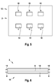
- FIG. 3 shows the plastic carrier substrate 1 of FIG. 1 in another plan view. Unlike the FIG. 1 Here, in each case a power semiconductor 9 is mounted on one of the power semiconductor terminals 3.
- the high-current connections 4 each lead to an outer edge of the plastic carrier substrate 1.
- the FIG. 4 shows the Kunststofflysubsubstrat 1 and the Entracermungssubstrat 6, which together form a component 10 of the power electronics module 2.
- the cooling substrate 6 is arranged on the plastic carrier substrate 1 in such a way that the power semiconductors 9 arranged on the plastic carrier substrate 1 engage in or pass through the recesses 8 of the cooling substrate 6.
- the Entracermungssubstrat 6 is slightly smaller than the plastic carrier substrate 1, so that an edge region of the plastic carrier substrate 1 is freely accessible, whereby the leading up to the edges of the plastic carrier substrate 1 high-current connections 4 can be electrically contacted.
- the plastic carrier substrate 1 and the Entracermungssubstrat 6 may have an equal outer contour, the high-current connections 4 then expediently beyond the outer edges of the plastic carrier substrate 1 extend / project.
- the recesses 8 of the Entracermungssubstrats 6 are advantageously formed larger than the power semiconductor 9, creating a gap 11 between the power semiconductors 9 and the edge of the recesses 8 of the Entracermungssubstrats 6.
- the gap 11 with a viscous heat conducting means 12 is filled which ensures a thermal connection of the power semiconductors 9 to the Entracermungssubstrat 6, so that the heat developed by the power semiconductors 9 heat can be dissipated in a simple manner. That in the Figures 1 and 2 shown Entracermungselement 5 is in the present embodiment with the Entracermungssubstrat 6 in contact (not shown here), so that there is a thermal connection here.
- the FIG. 5 shows an exemplary contacting substrate 13 of the power electronics module 2.
- the contacting substrate 13 is also flexible and has a plastic carrier substrate 1 corresponding contour.
- power semiconductor terminals 14 are arranged, which are formed as source terminals and on the other hand power semiconductor terminals 15, which as Gate terminals are formed. They are arranged in such a way that when the contacting substrate 13 is placed on the component 10, the power semiconductors 9 arranged on the plastic carrier substrate 2 are contacted.
- the FIG. 6 shows the complete power electronics module 2 in a side view.
- the component 10 which is formed by the plastic carrier substrate 1 and the Entracermungssubstrat 6, from the FIG. 5 known contacting substrate 13.
- the flexible design of the plastic carrier substrate 2, the Entracermungssubstrats 6 and the Kunststofftechnikssubstrats 13 a flexible power electronics module 2 is created.
- the power semiconductors 9 can be held clamped between the plastic carrier substrate 1 and the contacting substrate 13. Additionally or alternatively, the power semiconductors 9 may be mounted on the plastic carrier substrate 2 or the power semiconductor terminals 3, for example by gluing or soldering.
- both low-current connections 15 and high-current connections are arranged out of the contacting substrate 13 from the contacting substrate 13.
- the plastic carrier substrate 1, the Entracermungssubstrat 6, the contacting substrate 13 and the power semiconductor 9 and the electrical connections (4,14,15) in this case form an advantageous circuit carrier 16 of the power electronics module. 2
- the present power electronics module 2 offers on the one hand the already mentioned flexibility, on the other hand a particularly favorable heat dissipation of the heat developed by the power semiconductors 9.
- the power electronics module 2 can be contacted and / or fixed, for example, on a printed circuit board by soldering and / or a heat sink or by soldering connector pins.
- the power electronics module 2 present here represents a less expensive solution.
- the costs are reduced by the plastic carrier substrate 1 and, on the other hand, by avoiding soldering and / or wire bonding processes for connecting the power semiconductors 9.
Landscapes
- Engineering & Computer Science (AREA)
- Manufacturing & Machinery (AREA)
- Microelectronics & Electronic Packaging (AREA)
- Cooling Or The Like Of Semiconductors Or Solid State Devices (AREA)
- Structures Or Materials For Encapsulating Or Coating Semiconductor Devices Or Solid State Devices (AREA)
Abstract
Description
- Die Erfindung betrifft ein Leistungselektronikmodul mit mindestens einem Schaltungsträger und mindestens einem Leistungshalbleiter.
- Leistungselektronikmodule der eingangs genannten Art sind aus dem Stand der Technik bekannt. Diese weisen einen Schaltungsträger auf, an dem der Leistungshalbleiter angeordnet ist. Schaltungsträger und Leistungshalbleiter sind dabei fest miteinander verbunden, wobei in der Regel ein Schaltungsträger auf Keramikbasis (DCB/DBC = Direct Bonded Copper) oder Metallbasis (IMS = Integrated Metal Substrate/Metallplatte mit Isolation und Schaltung oder Stanzgitterlösungen) verwendet wird. Hierdurch wird sichergestellt, dass hohe Ströme transportiert und gleichzeitig entstehende beziehungsweise entstandene Wärme von dem Leistungshalbleiter oder den Leistungshalbleitern abgeführt werden kann. Thermisch günstige Schaltungsträger sind jedoch in ihrer Herstellung teuer und zur elektrischen Kontaktierung der Leistungshalbleiter sind eine Vielzahl von Lötprozessen und/oder Drahtbondprozessen notwendig.
- Die Erfindung sieht vor, dass der Schaltungsträger ein flexibles Kunststoffträgersubstrat, insbesondere mit Kupfer-Leiterbahnen, aufweist, auf dem der Leistungshalbleiter montiert ist, dass der Schaltungsträger ein flexibles Entwärmungssubstrat aufweist, das flächig auf dem Kunststoffträgersubstrat angeordnet ist und dass der Schaltungsträger ein flexibles Kontaktierungssubstrat aufweist, das flächig auf dem sich aus Kunststoffträgersubstrat und Entwärmungssubstrat zusammensetzenden Bauteil angeordnet ist. Es ist also ein Schaltungsträger mit einem schichtartigen Aufbau vorgesehen, wobei die Basis von dem Kunststoffträgersubstrat gebildet ist, welches vorteilhafterweise flexibel gestaltet ist. Auf diesem ist der Leistungshalbleiter montiert. Im Gegensatz zu einem aus dem Stand der Technik bekannten Schaltungsträger ist der vorliegende Schaltungsträger aufgrund der Verwendung des Kunststoffträgersubstrats günstiger und einfacher herstellbar. Das Entwärmungssubstrat dient zum Abführen beziehungsweise Spreizen und Verteilen der Wärme von dem Leistungshalbleiter beziehungsweise dem Schaltungsträger. Letztendlich wird die Wärme über Kupfer auf dem Kunststoffträgersubstrat und dem Kontaktierungssubstrat abgeführt. Es ist ebenfalls flexibel ausgebildet und ist flächig auf dem Kunststoffträgersubstrat angeordnet, sodass das Entwärmungssubstrat das Kunststoffträgersubstrat vorteilhafterweise im Wesentlichen abdeckt, wobei besonders bevorzugt das Entwärmungssubstrat etwas kleiner ausgebildet ist, sodass ein Randbereich des Kunststoffträgersubstrat frei zugängig ist. Hierdurch wird ein einfaches Kontaktieren von auf dem Kunststoffträgersubstrat angeordneten elektrischen Kontakten, die von oder zu dem Leistungshalbleiter führen, gewährleistet. Das Kunststoffträgersubstrat und das Entwärmungssubstrat bilden zusammen ein Bauteil, auf dem das Kontaktierungssubstrat flächig angeordnet ist. Da sowohl das Kunststoffträgersubstrat, das Entwärmungssubstrat als auch das Kontaktierungssubstrat flexibel ausgebildet sind, wird ein flexibles Leistungselektronikmodul zur Verfügung gestellt. Wobei die Flexibilität des Leistungselektronikmoduls natürlich auch von weiteren Faktoren, wie der Größe und Anzahl von auf dem Schaltungsträger angeordneten Leiterbahnen und/oder den Dimensionen sowie der Anzahl der Leistungshalbleiter abhängig ist. Durch die flexible Ausgestaltung wird zum Einen die Zuverlässigkeit des Leistungselektronikmoduls auf lange Sicht hin erhöht, da es sich an verändernde Umgebungsbedingungen sowie Form- und/oder Lagetoleranzen anpassen kann, und zum Anderen wird durch das Entwärmungssubstrat eine besonders günstige Entwärmung des Leistungselektronikmoduls gewährleistet.
- Nach einer Weiterbildung der Erfindung weist das Entwärmungssubstrat mindestens eine Ausnehmung zur Aufnahme des Leistungshalbleiters auf. Der Leistungshalbleiter ragt somit in das Entwärmungssubstrat hinein oder durch dieses hindurch, wodurch zum Einen die Wärmeabfuhr von von dem Leistungshalbleiter entwickelter Wärme erhöht und erleichtert wird und zum Anderen der Leistungshalbleiter von dem Kontaktiersubstrat kontaktiert werden kann. Vorteilhafterweise sind an dem Kunststoffträgersubstrat und an dem Kontaktierungssubstrat auf den zueinander weisenden Seiten Kontaktelemente und/oder Leiterbahnen angeordnet, über die der Leistungshalbleiter elektrisch kontaktiert werden kann.
- Nach einer Weiterbildung der Erfindung weist das Kunststoffträgersubstrat mindestens eine mit dem Leistungshalbleiter verbundene Hochstromverbindung auf. Die Hochstromverbindung führt vorteilhafterweise bis zu dem Randbereich des Kunststoffträgersubstrats, der frei zugängig ist, sodass die Hochstromverbindung von außen auf einfache Art und Weise elektrisch kontaktiert werden kann. Vorteilhafterweise ist das Kunststoffträgersubstrat ein Polyimidsubstrat, insbesondere mit Kupfer-Leiterbahnen.
- Weiterhin ist vorgesehen, dass das Kontaktiersubstrat mindestens eine Niederstrom- und/oder eine Hochstromverbindung für den Leistungshalbleiter aufweist. Zweckmäßigerweise ist die Hochstromverbindung des Kunststoffträgersubstrats mit dem Drain-Anschluss des Leistungshalbleiters verbunden. Weiterhin sind die Niederstrom- und/oder Hochstromverbindungen des Kontaktierungssubstrats mit Gate- und/oder Source-Anschlüssen des Leistungshalbleiters verbunden.
- Mit Vorteil ist vorgesehen, dass das Entwärmungssubstrat eine Graphit-Folie ist. Diese kann auf einfache Art und Weise, zum Beispiel durch Stanzen, Lasern oder Ähnlichem, "zugeschnitten" und auf dem Kunststoffträgersubstrat angeordnet werden. Derartige Graphit-Folien sind kostengünstig herstellbar.
- Bevorzugt ist zwischen dem Entwärmungssubstrat und dem Leistungshalbleiter ein Wärmeleitmittel (Gap-Filler) angeordnet. Dadurch wird der Leistungshalbleiter thermisch an das Entwärmungssubstrat beziehungsweise die Graphitfolie angebunden, sodass eine besonders günstige Entwärmung des Leistungshalbleiters erfolgt. Das vorteilhafterweise viskose Wärmeleitmittel dient somit als thermisches Kontaktmittel zwischen Leistungshalbleiter und Entwärmungssubstrat.
- In einer bevorzugten Ausführungsform der Erfindung weist das Kunststoffträgersubstrat und/oder das Entwärmungssubstrat mindestens ein Entwärmungsflächenelement auf, das mit dem Entwärmungssubstrat in thermischen Kontakt steht. Über das Entwärmungsflächenelement kann beispielsweise auch Wärme von dem Kunststoffträgersubstrat auf das Entwärmungssubstrat übertragen werden. In einer alternativen Ausführungsform ist das Entwärmungsflächenelement auf dem Kunststoffträgersubstrat angeordnet und steht nicht in thermischem Kontakt mit dem Entwärmungssubstrat, sodass es lediglich als Entwärmungspad für das Kunststoffträgersubstrat dient.
- In einer vorteilhaften Weiterbildung der Erfindung sind die Leistungshalbleiter durch Verklebung und/oder Lötung auf dem Kunststoffträgersubstrat montiert.
- Alternativ oder zusätzlich ist vorgesehen, dass der Leistungshalbleiter zwischen dem Kunststoffträgersubstrat und dem Entwärmungssubstrat (im montierten Zustand) klemmend gehalten ist. Hierbei wird der Leistungshalbleiter zum Beispiel durch das Kontaktierungssubstrat auf das Kunststoffträgersubstrat gedrückt und somit in einer festen Position gehalten. Dies ermöglicht eine besonders einfache und schnelle Montage des Leistungselektronikmoduls.
- Im Folgenden soll die Erfindung anhand einiger Figuren näher erläutert werden. Dazu zeigen
- Figur 1
- ein Ausführungsbeispiel eines vorteilhaften Kunststoffträgersubstrats eines Leistungselektronikmoduls in einer Draufsicht,
- Figur 2
- ein vorteilhaftes Entwärmungssubstrat des Leistungselektronikmoduls in einer Draufsicht,
- Figur 3
- das Kunststoffträgersubstrat des Leistungselektronikmoduls in einer weiteren Draufsicht mit Leistungshalbleitern,
- Figur 4
- das Kunststoffträgersubstrat und das Entwärmungssubstrat in einer Draufsicht,
- Figur 5
- ein vorteilhaftes Kontaktierungssubstrat des Leistungselektronikmoduls in einer Draufsicht und
- Figur 6
- einen Schaltungsträger des Leistungselektronikmoduls in einer Seitenansicht.
- Die
Figur 1 zeigt in einem Ausführungsbeispiel der Erfindung ein Kunststoffträgersubstrat 1 eines Leistungselektronikmoduls 2 in einer Draufsicht. Das Kunststoffträgersubstrat 1 ist im Wesentlichen rechteckförmig ausgebildet. Auf dem Kunststoffträgersubstrat 1 sind mehrere Leistungshalbleiteranschlüsse 3 angeordnet, die mit auf dem Kunststoffträgersubstrat 1 angeordneten Hochstromverbindungen 4 elektrisch verbunden sind. In dem vorliegenden Ausführungsbeispiel sind die Leistungshalbleiteranschlüsse 3 jeweils als Drain-Anschluss ausgebildet. Das Kunststoffträgersubstrat 1 ist vorteilhafterweise flexibel ausgebildet. Weiterhin ist auf dem Kunststoffträgersubstrat 1 ein Entwärmungselement 5 angeordnet, welches beispielsweise als Wärmespeicher dienen kann. - Die
Figur 2 zeigt in einer Draufsicht ein Entwärmungssubstrat 6 des Leistungselektronikmoduls 2. Das Entwärmungssubstrat 6 ist von einer flexiblen Graphitfolie 7 gebildet. Seine Kontur entspricht im Wesentlichen der Kontur des in derFigur 1 dargestellten Kunststoffträgersubstrats 1. In dem Entwärmungssubstrat 6 sind mehrere Ausnehmungen 8 ausgebildet, deren Form und Anordnung im Wesentlichen der auf dem Kunststoffträgersubstrat 1 angeordneten Leistungshalbeiteranschlüsse 3 (Figur 1 ) entsprechen. - Die
Figur 3 zeigt das Kunststoffträgersubstrat 1 derFigur 1 in einer weiteren Draufsicht. Im Unterschied zu derFigur 1 ist hierbei jeweils ein Leistungshalbleiter 9 auf einem der Leistungshalbleiteranschlüsse 3 montiert. - Die Hochstromverbindungen 4 führen jeweils bis zu einer Außenkante des Kunststoffträgersubstrats 1.
- Die
Figur 4 zeigt das Kunststoffträgersubsubstrat 1 und das Entwärmungssubstrat 6, die zusammen ein Bauteil 10 des Leistungselektronikmoduls 2 bilden. Dabei ist das Entwärmungssubstrat 6 derart auf dem Kunststoffträgersubstrat 1 angeordnet, dass die auf dem Kunststoffträgersubstrat 1 angeordneten Leistungshalbleiter 9 in den Ausnehmungen 8 des Entwärmungssubstrats 6 einliegen beziehungsweise durch diese hindurchgreifen. Das Entwärmungssubstrat 6 ist etwas kleiner ausgebildet als das Kunststoffträgersubstrat 1, sodass ein Randbereich des Kunststoffträgersubstrats 1 frei zugängig ist, wodurch die bis an die Kanten des Kunststoffträgersubstrats 1 führenden Hochstromverbindungen 4 elektrisch kontaktiert werden können. Alternativ dazu können das Kunststoffträgersubstrat 1 und das Entwärmungssubstrat 6 eine gleich große Außenkontur aufweisen, wobei die Hochstromverbindungen 4 dann zweckmäßigerweise über die Außenkanten des Kunststoffträgersubstrats 1 hinausführen/ragen. Da die Ausnehmungen 8 des Entwärmungssubstrats 6 vorteilhafterweise größer ausgebildet sind als die Leistungshalbleiter 9, entsteht ein Spalt 11 zwischen den Leistungshalbleitern 9 und dem Rand der Ausnehmungen 8 des Entwärmungssubstrats 6. Vorteilhafterweise ist der Spalt 11 mit einem viskosen Wärmeleitmittel 12 (Gap-Filler) gefüllt, das eine thermische Anbindung der Leistungshalbleiter 9 an das Entwärmungssubstrat 6 gewährleistet, sodass die von den Leistungshalbleitern 9 entwickelte Wärme auf einfache Art und Weise abgeführt werden kann. Das in denFiguren 1 und 2 dargestellte Entwärmungselement 5 steht in dem vorliegenden Ausführungsbeispiel mit dem Entwärmungssubstrat 6 in Kontakt (hier nicht dargestellt), sodass auch hier eine thermische Verbindung besteht. - Die
Figur 5 zeigt ein beispielhaftes Kontaktierungssubstrat 13 des Leistungselektronikmoduls 2. Das Kontaktierungssubstrat 13 ist ebenfalls flexibel ausgebildet und weist eine dem Kunststoffträgersubstrat 1 entsprechende Kontur auf. Auf dem Kontaktierungssubstrat 13 sind zum Einen Leistungshalbleiteranschlüsse 14 angeordnet, die als Source-Anschlüsse ausgebildet sind und zum Anderen Leistungshalbleiteranschlüsse 15, die als Gate-Anschlüsse ausgebildet sind. Sie sind derart angeordnet, dass wenn das Kontaktierungssubstrat 13 auf das Bauteil 10 gelegt wird, die auf dem Kunststoffträgersubstrat 2 angeordneten Leistungshalbleiter 9 kontaktiert werden. - Die
Figur 6 zeigt dazu das vollständige Leistungselektronikmodul 2 in einer Seitenansicht. Hierbei liegt auf dem Bauteil 10, das von dem Kunststoffträgersubstrat 1 und dem Entwärmungssubstrat 6 gebildet wird, das aus derFigur 5 bekannte Kontaktierungssubstrat 13 auf. Durch die flexible Ausbildung des Kunststoffträgersubstrats 2, des Entwärmungssubstrats 6 sowie des Kontaktierungssubstrats 13 ist ein flexibles Leistungselektronikmodul 2 geschaffen. Die Leistungshalbleiter 9 können dabei zwischen dem Kunststoffträgersubstrat 1 und dem Kontaktierungssubstrat 13 eingeklemmt gehalten werden. Zusätzlich oder alternativ können die Leistungshalbleiter 9 auf dem Kunststoffträgersubstrat 2 beziehungsweise den Leistungshalbleiteranschlüssen 3 beispielsweise durch Verkleben oder Verlöten montiert sein. - Weiterhin zeigt die
Figur 6 von dem Kunststoffträgersubstrat 1 abstehende Hochstromverbindungen 4, die oben bereits als alternative Ausbildungen der Hochstromverbindungen genannt wurden, und von dem Kontaktierungssubstrat 13 ausgehende Niederstromverbindungen 15.Vorteilhafterweise sind aus dem Kontaktierungssubstrat 13 sowohl Niederstromverbindungen 15 sowie Hochstromverbindungen angeordnet. Das Kunststoffträgersubstrat 1, das Entwärmungssubstrat 6, das Kontaktierungssubstrat 13 sowie die Leistungshalbleiter 9 und die elektrischen Verbindungen (4,14,15) bilden hierbei einen vorteilhaften Schaltungsträger 16 des Leistungselektronikmoduls 2. - Das vorliegende Leistungselektronikmodul 2 bietet zum Einen die bereits genannte Flexibilität, zum Anderen eine besonders günstige Wärmeabfuhr der von den Leistungshalbleitern 9 entwickelten Wärme. Das Leistungselektronikmodul 2 kann beispielsweise auf einer Leiterplatte durch Auflöten und/oder eine Heatsink oder durch Anlöten von Steckerpins kontaktiert und/oder befestigt werden.
- Im Vergleich zu herkömmlichen Schaltungsträgern, insbesondere keramischen Schaltungsträgern, stellt das hier vorliegende Leistungselektronikmodul 2 eine kostengünstigere Lösung dar. Zum Einen werden die Kosten durch das Kunststoffträgersubstrat 1 und zum Anderen durch die Vermeidung von Löt- und/oder Drahtbondprozessen zur Anbindung der Leistungshalbleitern 9 verringert.
Claims (10)
- Leistungselektronikmodul mit mindestens einem Schaltungsträger und mindestens einem Leistungshalbleiter, dadurch gekennzeichnet, dass der Schaltungsträger (16) ein flexibles Kunststoffträgersubstrat (1) aufweist, auf dem der Leistungshalbleiter (9) montiert ist, dass der Schaltungsträger (16) ein flexibles Entwärmungssubstrat (6) aufweist, das flächig auf dem Kunststoffträgersubstrat (1) angeordnet ist und dass der Schaltungsträger (16) ein flexibles Kontaktierungssubstrat (13) aufweist, das flächig auf dem sich aus Kunststoffträgersubstrat (1) und Entwärmungssubstrat (6) zusammensetzenden Bauteil (10) angeordnet ist.
- Leistungselektronikmodul nach Anspruch 1, dadurch gekennzeichnet, dass das Entwärmungssubstrat (6) mindestens eine Ausnehmung (8) zur Aufnahme des Leistungshalbleiters (9) aufweist.
- Leistungselektronikmodul nach einem der vorhergehenden Ansprüche, dadurch gekennzeichnet, dass das Kunststoffträgersubstrat (1) mindestens eine mit dem Leistungshalbleiter (9) verbundene Hochstromverbindung (4) aufweist.
- Leistungselektronikmodul nach einem der vorhergehenden Ansprüche, dadurch gekennzeichnet, dass das Kontaktierungssubstrat (13) mindestens eine Niederstrom- und/oder Hochstromverbindung (15) für den Leistungshalbleiter (9) aufweist.
- Leistungselektronikmodul nach einem der vorhergehenden Ansprüche, dadurch gekennzeichnet, dass das Entwärmungssubstrat (6) eine Graphit-Folie (7) ist.
- Leistungselektronikmodul nach einem der vorhergehenden Ansprüche, dadurch gekennzeichnet, dass zwischen Entwärmungssubstrat (6) und Leistungshableiter (9) ein Wärmeleitmittel (12) (Gap-Filler) angeordnet ist.
- Leistungselektronikmodul nach einem der vorhergehenden Ansprüche, dadurch gekennzeichnet, dass das Kunststoffträgersubstrat (1) ein Polyimidsubstrat ist.
- Leistungselektronikmodul nach einem der vorhergehenden Ansprüche, dadurch gekennzeichnet, dass das Kunststoffträgersubstrat (1) mindestens ein Entwärmungsflächenelement (5) aufweist, das mit dem Entwärmungssubstrat (6) in thermischen Kontakt steht.
- Leistungselektronikmodul nach einem der vorhergehenden Ansprüche, dadurch gekennzeichnet, dass der Leistungshalbleiter (9) durch Verklebung und/oder Lötung auf dem Kunststoffträgersubstrat (1) montiert ist.
- Leistungselektronikmodul nach einem der vorhergehenden Ansprüche, dadurch gekennzeichnet, dass der Leistungshalbleiter (9) zwischen dem Kunststoffträgersubstrat (1) und dem Kontaktierungssubstrat (13) klemmend gehalten ist.
Applications Claiming Priority (1)
| Application Number | Priority Date | Filing Date | Title |
|---|---|---|---|
| DE102007027901A DE102007027901A1 (de) | 2007-06-18 | 2007-06-18 | Leistungselektronikmodul |
Publications (3)
| Publication Number | Publication Date |
|---|---|
| EP2006910A2 true EP2006910A2 (de) | 2008-12-24 |
| EP2006910A3 EP2006910A3 (de) | 2010-07-28 |
| EP2006910B1 EP2006910B1 (de) | 2016-03-16 |
Family
ID=39686712
Family Applications (1)
| Application Number | Title | Priority Date | Filing Date |
|---|---|---|---|
| EP08104205.3A Ceased EP2006910B1 (de) | 2007-06-18 | 2008-06-02 | Leistungselektronikmodul |
Country Status (2)
| Country | Link |
|---|---|
| EP (1) | EP2006910B1 (de) |
| DE (1) | DE102007027901A1 (de) |
Cited By (3)
| Publication number | Priority date | Publication date | Assignee | Title |
|---|---|---|---|---|
| WO2012139935A1 (de) * | 2011-04-12 | 2012-10-18 | BSH Bosch und Siemens Hausgeräte GmbH | Kühlvorrichtung für ein elektronikmodul eines haushaltsgeräts sowie baugruppe und haushaltsgerät mit einer kühlvorrichtung |
| EP3022765A4 (de) * | 2014-09-26 | 2017-04-26 | Intel Corporation | Flexible verpackungsarchitektur |
| WO2018072925A1 (de) * | 2016-10-20 | 2018-04-26 | Robert Bosch Gmbh | Leistungsmodul |
Families Citing this family (1)
| Publication number | Priority date | Publication date | Assignee | Title |
|---|---|---|---|---|
| DE102009035850A1 (de) | 2009-07-31 | 2011-02-03 | Vossloh-Schwabe Optoelectronic Gmbh & Co. Kg | Leiterplattenordnung mit Keramikplatte und Grafitschicht |
Family Cites Families (1)
| Publication number | Priority date | Publication date | Assignee | Title |
|---|---|---|---|---|
| JP2006165175A (ja) * | 2004-12-06 | 2006-06-22 | Alps Electric Co Ltd | 回路部品モジュールおよび電子回路装置並びに回路部品モジュールの製造方法 |
-
2007
- 2007-06-18 DE DE102007027901A patent/DE102007027901A1/de not_active Withdrawn
-
2008
- 2008-06-02 EP EP08104205.3A patent/EP2006910B1/de not_active Ceased
Cited By (7)
| Publication number | Priority date | Publication date | Assignee | Title |
|---|---|---|---|---|
| WO2012139935A1 (de) * | 2011-04-12 | 2012-10-18 | BSH Bosch und Siemens Hausgeräte GmbH | Kühlvorrichtung für ein elektronikmodul eines haushaltsgeräts sowie baugruppe und haushaltsgerät mit einer kühlvorrichtung |
| CN103460378A (zh) * | 2011-04-12 | 2013-12-18 | Bsh博世和西门子家用电器有限公司 | 用于家用器具电子模块的冷却装置以及具有冷却装置的组件和家用器具 |
| CN103460378B (zh) * | 2011-04-12 | 2016-08-24 | Bsh家用电器有限公司 | 用于家用器具电子模块的冷却装置以及具有冷却装置的组件和家用器具 |
| EP3022765A4 (de) * | 2014-09-26 | 2017-04-26 | Intel Corporation | Flexible verpackungsarchitektur |
| US10396038B2 (en) | 2014-09-26 | 2019-08-27 | Intel Corporation | Flexible packaging architecture |
| WO2018072925A1 (de) * | 2016-10-20 | 2018-04-26 | Robert Bosch Gmbh | Leistungsmodul |
| US10892207B2 (en) | 2016-10-20 | 2021-01-12 | Robert Bosch Gmbh | Power module |
Also Published As
| Publication number | Publication date |
|---|---|
| EP2006910A3 (de) | 2010-07-28 |
| DE102007027901A1 (de) | 2008-12-24 |
| EP2006910B1 (de) | 2016-03-16 |
Similar Documents
| Publication | Publication Date | Title |
|---|---|---|
| DE102014212519B4 (de) | Halbleitervorrichtung | |
| EP1450404B1 (de) | Anordnung in Druckkontaktierung mit einem Leistungshalbleitermodul | |
| EP1592063B1 (de) | Anordnung in Druckkontaktierung mit einem Leistungshalbleitermodul | |
| DE102004060935B4 (de) | Leistungshalbleitervorrichtung | |
| EP3794641B1 (de) | Entwärmungsanordnung für ein halbleiterleistungsmodul | |
| WO2011113867A1 (de) | Schaltungseinheit mit stromschiene zur strom- und wärmeübertragung sowie ein verfahren zur herstellung dieser schaltungseinheit | |
| DE102016208029A1 (de) | Halbleitervorrichtung | |
| DE102006047989A1 (de) | Halbleitervorrichtung | |
| DE112016005807T5 (de) | Halbleitereinheit und Verfahren zur Herstellung derselben | |
| DE102020105267A1 (de) | Halbleitervorrichtung und Verfahren zur Herstellung derselben | |
| DE202020101852U1 (de) | Thermische Schnittstelle für mehrere diskrete elektronische Vorrichtungen | |
| EP1265282B1 (de) | Schaltungsanordnung | |
| DE102016105783B4 (de) | Leistungshalbleitereinrichtung | |
| EP2006910B1 (de) | Leistungselektronikmodul | |
| DE102006008807B4 (de) | Anordnung mit einem Leistungshalbleitermodul und einem Kühlbauteil | |
| WO2024056459A1 (de) | Halbbrückenmodul | |
| DE10249205B3 (de) | Leistungsbauelementanordnung zur mechatronischen Integration von Leistungsbauelementen | |
| DE102019210902A1 (de) | Verbindungsmethode für leistungsmodule mit einer zwischenkreisverschienung | |
| DE102004030443A1 (de) | Steuergerät | |
| DE112017001346T5 (de) | Schaltungsanordnung | |
| DE102021134001B4 (de) | Leistungshalbleitermodul mit einem Substrat, Leistungshalbleiterbauelementen und mit einem Druckkörper und Leistungshalbleitereinrichtung damit | |
| DE202016101292U1 (de) | Leistungshalbleitereinrichtung | |
| DE102006040838B4 (de) | Elektronische Leistungspackung mit zwei Substraten mit mehreren Halbleiterchips und elektronischen Komponenten | |
| DE202013010288U1 (de) | Frequenzumrichter mit Zwischenkreiskondensator | |
| DE102018217607A1 (de) | Halbleiterbauelement-Anordnung, Verfahren zu deren Herstellung sowie Entwärmungseinrichtung |
Legal Events
| Date | Code | Title | Description |
|---|---|---|---|
| PUAI | Public reference made under article 153(3) epc to a published international application that has entered the european phase |
Free format text: ORIGINAL CODE: 0009012 |
|
| AK | Designated contracting states |
Kind code of ref document: A2 Designated state(s): AT BE BG CH CY CZ DE DK EE ES FI FR GB GR HR HU IE IS IT LI LT LU LV MC MT NL NO PL PT RO SE SI SK TR |
|
| AX | Request for extension of the european patent |
Extension state: AL BA MK RS |
|
| PUAL | Search report despatched |
Free format text: ORIGINAL CODE: 0009013 |
|
| AK | Designated contracting states |
Kind code of ref document: A3 Designated state(s): AT BE BG CH CY CZ DE DK EE ES FI FR GB GR HR HU IE IS IT LI LT LU LV MC MT NL NO PL PT RO SE SI SK TR |
|
| AX | Request for extension of the european patent |
Extension state: AL BA MK RS |
|
| RIC1 | Information provided on ipc code assigned before grant |
Ipc: H01L 23/373 20060101AFI20080821BHEP Ipc: H01L 23/538 20060101ALI20100623BHEP Ipc: H01L 25/07 20060101ALI20100623BHEP Ipc: H01L 25/065 20060101ALI20100623BHEP |
|
| 17P | Request for examination filed |
Effective date: 20110128 |
|
| AKX | Designation fees paid |
Designated state(s): DE ES FR GB IT |
|
| 17Q | First examination report despatched |
Effective date: 20131014 |
|
| GRAP | Despatch of communication of intention to grant a patent |
Free format text: ORIGINAL CODE: EPIDOSNIGR1 |
|
| INTG | Intention to grant announced |
Effective date: 20151022 |
|
| GRAS | Grant fee paid |
Free format text: ORIGINAL CODE: EPIDOSNIGR3 |
|
| GRAA | (expected) grant |
Free format text: ORIGINAL CODE: 0009210 |
|
| AK | Designated contracting states |
Kind code of ref document: B1 Designated state(s): DE ES FR GB IT |
|
| REG | Reference to a national code |
Ref country code: GB Ref legal event code: FG4D Free format text: NOT ENGLISH |
|
| REG | Reference to a national code |
Ref country code: DE Ref legal event code: R096 Ref document number: 502008013919 Country of ref document: DE |
|
| REG | Reference to a national code |
Ref country code: FR Ref legal event code: PLFP Year of fee payment: 9 |
|
| PG25 | Lapsed in a contracting state [announced via postgrant information from national office to epo] |
Ref country code: ES Free format text: LAPSE BECAUSE OF FAILURE TO SUBMIT A TRANSLATION OF THE DESCRIPTION OR TO PAY THE FEE WITHIN THE PRESCRIBED TIME-LIMIT Effective date: 20160316 |
|
| REG | Reference to a national code |
Ref country code: DE Ref legal event code: R097 Ref document number: 502008013919 Country of ref document: DE |
|
| PG25 | Lapsed in a contracting state [announced via postgrant information from national office to epo] |
Ref country code: IT Free format text: LAPSE BECAUSE OF FAILURE TO SUBMIT A TRANSLATION OF THE DESCRIPTION OR TO PAY THE FEE WITHIN THE PRESCRIBED TIME-LIMIT Effective date: 20160316 |
|
| PLBE | No opposition filed within time limit |
Free format text: ORIGINAL CODE: 0009261 |
|
| STAA | Information on the status of an ep patent application or granted ep patent |
Free format text: STATUS: NO OPPOSITION FILED WITHIN TIME LIMIT |
|
| 26N | No opposition filed |
Effective date: 20161219 |
|
| GBPC | Gb: european patent ceased through non-payment of renewal fee |
Effective date: 20160616 |
|
| PG25 | Lapsed in a contracting state [announced via postgrant information from national office to epo] |
Ref country code: GB Free format text: LAPSE BECAUSE OF NON-PAYMENT OF DUE FEES Effective date: 20160616 |
|
| REG | Reference to a national code |
Ref country code: FR Ref legal event code: PLFP Year of fee payment: 10 |
|
| REG | Reference to a national code |
Ref country code: FR Ref legal event code: PLFP Year of fee payment: 11 |
|
| PGFP | Annual fee paid to national office [announced via postgrant information from national office to epo] |
Ref country code: FR Payment date: 20190625 Year of fee payment: 12 |
|
| PGFP | Annual fee paid to national office [announced via postgrant information from national office to epo] |
Ref country code: DE Payment date: 20190822 Year of fee payment: 12 |
|
| REG | Reference to a national code |
Ref country code: DE Ref legal event code: R119 Ref document number: 502008013919 Country of ref document: DE |
|
| PG25 | Lapsed in a contracting state [announced via postgrant information from national office to epo] |
Ref country code: FR Free format text: LAPSE BECAUSE OF NON-PAYMENT OF DUE FEES Effective date: 20200630 |
|
| PG25 | Lapsed in a contracting state [announced via postgrant information from national office to epo] |
Ref country code: DE Free format text: LAPSE BECAUSE OF NON-PAYMENT OF DUE FEES Effective date: 20210101 |