EP2006908A2 - Electronic device and method of manufacturing the same - Google Patents
Electronic device and method of manufacturing the same Download PDFInfo
- Publication number
- EP2006908A2 EP2006908A2 EP08158703A EP08158703A EP2006908A2 EP 2006908 A2 EP2006908 A2 EP 2006908A2 EP 08158703 A EP08158703 A EP 08158703A EP 08158703 A EP08158703 A EP 08158703A EP 2006908 A2 EP2006908 A2 EP 2006908A2
- Authority
- EP
- European Patent Office
- Prior art keywords
- layer
- insulating layer
- forming
- bumps
- stress absorbing
- Prior art date
- Legal status (The legal status is an assumption and is not a legal conclusion. Google has not performed a legal analysis and makes no representation as to the accuracy of the status listed.)
- Granted
Links
Images






Classifications
-
- H—ELECTRICITY
- H10—SEMICONDUCTOR DEVICES; ELECTRIC SOLID-STATE DEVICES NOT OTHERWISE PROVIDED FOR
- H10W—GENERIC PACKAGES, INTERCONNECTIONS, CONNECTORS OR OTHER CONSTRUCTIONAL DETAILS OF DEVICES COVERED BY CLASS H10
- H10W72/00—Interconnections or connectors in packages
-
- H—ELECTRICITY
- H10—SEMICONDUCTOR DEVICES; ELECTRIC SOLID-STATE DEVICES NOT OTHERWISE PROVIDED FOR
- H10W—GENERIC PACKAGES, INTERCONNECTIONS, CONNECTORS OR OTHER CONSTRUCTIONAL DETAILS OF DEVICES COVERED BY CLASS H10
- H10W74/00—Encapsulations, e.g. protective coatings
- H10W74/10—Encapsulations, e.g. protective coatings characterised by their shape or disposition
- H10W74/111—Encapsulations, e.g. protective coatings characterised by their shape or disposition the semiconductor body being completely enclosed
- H10W74/129—Encapsulations, e.g. protective coatings characterised by their shape or disposition the semiconductor body being completely enclosed forming a chip-scale package [CSP]
-
- H—ELECTRICITY
- H10—SEMICONDUCTOR DEVICES; ELECTRIC SOLID-STATE DEVICES NOT OTHERWISE PROVIDED FOR
- H10W—GENERIC PACKAGES, INTERCONNECTIONS, CONNECTORS OR OTHER CONSTRUCTIONAL DETAILS OF DEVICES COVERED BY CLASS H10
- H10W72/00—Interconnections or connectors in packages
- H10W72/01—Manufacture or treatment
- H10W72/012—Manufacture or treatment of bump connectors, dummy bumps or thermal bumps
-
- H—ELECTRICITY
- H10—SEMICONDUCTOR DEVICES; ELECTRIC SOLID-STATE DEVICES NOT OTHERWISE PROVIDED FOR
- H10W—GENERIC PACKAGES, INTERCONNECTIONS, CONNECTORS OR OTHER CONSTRUCTIONAL DETAILS OF DEVICES COVERED BY CLASS H10
- H10W72/00—Interconnections or connectors in packages
- H10W72/20—Bump connectors, e.g. solder bumps or copper pillars; Dummy bumps; Thermal bumps
-
- H—ELECTRICITY
- H10—SEMICONDUCTOR DEVICES; ELECTRIC SOLID-STATE DEVICES NOT OTHERWISE PROVIDED FOR
- H10W—GENERIC PACKAGES, INTERCONNECTIONS, CONNECTORS OR OTHER CONSTRUCTIONAL DETAILS OF DEVICES COVERED BY CLASS H10
- H10W70/00—Package substrates; Interposers; Redistribution layers [RDL]
- H10W70/01—Manufacture or treatment
- H10W70/05—Manufacture or treatment of insulating or insulated package substrates, or of interposers, or of redistribution layers
-
- H—ELECTRICITY
- H10—SEMICONDUCTOR DEVICES; ELECTRIC SOLID-STATE DEVICES NOT OTHERWISE PROVIDED FOR
- H10W—GENERIC PACKAGES, INTERCONNECTIONS, CONNECTORS OR OTHER CONSTRUCTIONAL DETAILS OF DEVICES COVERED BY CLASS H10
- H10W70/00—Package substrates; Interposers; Redistribution layers [RDL]
- H10W70/60—Insulating or insulated package substrates; Interposers; Redistribution layers
-
- H—ELECTRICITY
- H10—SEMICONDUCTOR DEVICES; ELECTRIC SOLID-STATE DEVICES NOT OTHERWISE PROVIDED FOR
- H10W—GENERIC PACKAGES, INTERCONNECTIONS, CONNECTORS OR OTHER CONSTRUCTIONAL DETAILS OF DEVICES COVERED BY CLASS H10
- H10W70/00—Package substrates; Interposers; Redistribution layers [RDL]
- H10W70/60—Insulating or insulated package substrates; Interposers; Redistribution layers
- H10W70/62—Insulating or insulated package substrates; Interposers; Redistribution layers characterised by their interconnections
- H10W70/65—Shapes or dispositions of interconnections
- H10W70/654—Top-view layouts
- H10W70/656—Fan-in layouts
-
- H—ELECTRICITY
- H10—SEMICONDUCTOR DEVICES; ELECTRIC SOLID-STATE DEVICES NOT OTHERWISE PROVIDED FOR
- H10W—GENERIC PACKAGES, INTERCONNECTIONS, CONNECTORS OR OTHER CONSTRUCTIONAL DETAILS OF DEVICES COVERED BY CLASS H10
- H10W72/00—Interconnections or connectors in packages
- H10W72/20—Bump connectors, e.g. solder bumps or copper pillars; Dummy bumps; Thermal bumps
- H10W72/251—Materials
- H10W72/252—Materials comprising solid metals or solid metalloids, e.g. PbSn, Ag or Cu
-
- H—ELECTRICITY
- H10—SEMICONDUCTOR DEVICES; ELECTRIC SOLID-STATE DEVICES NOT OTHERWISE PROVIDED FOR
- H10W—GENERIC PACKAGES, INTERCONNECTIONS, CONNECTORS OR OTHER CONSTRUCTIONAL DETAILS OF DEVICES COVERED BY CLASS H10
- H10W72/00—Interconnections or connectors in packages
- H10W72/20—Bump connectors, e.g. solder bumps or copper pillars; Dummy bumps; Thermal bumps
- H10W72/29—Bond pads specially adapted therefor
Definitions
- the present disclosure relates to an electronic device and a method of manufacturing the same and, more particularly, to an electronic device having bumps serving as external connection terminals, e.g. on a conductive pattern formed on an insulating layer, and a method of manufacturing the same.
- This chip size package has such a structure that the rewirings (the conductive layers) are formed on a device forming surface of a semiconductor chip, which is formed by dicing a wafer serving as a semiconductor substrate, via an insulating layer (passivation layer).
- this chip size package firstly a plurality of electrodes are formed on a semiconductor chip area of a semiconductor wafer, and then bumps are formed on respective electrodes by the wire bonding technology, for example.
- the bump is formed of the bonding wire by using the bonding machine.
- an insulating layer for protecting a circuit surface formed on the wafer is formed on the semiconductor wafer on which the bumps are formed. At this time, top end portions of the bumps are formed to expose from the insulating layer.
- the rewirings are formed over the insulating layer by the plating method, the printing method, or the like, for example. Then, the solder bumps serving as the external connection terminals are bonded to the rewirings, and then the wafer is cut into individual pieces by the dicing. Thus, the chip size package is manufactured (see e.g., JP-A-2002-313985 ).
- solder bumps serving as the external connection terminals are bonded to the rewirings formed on the insulating layer, when there is a difference in coefficient of thermal expansion between the semiconductor chip and the mounting substrate, a difference of thermal expansion due to the heating occurs between the semiconductor chip and the mounting substrate upon mounting the semiconductor device on the mounting substrate.
- Exemplary embodiments of the present invention address the above disadvantages and other disadvantages not described above.
- the present invention is not required to overcome the disadvantages described above, and thus, an exemplary embodiment of the present invention may not overcome any of the problems described above.
- a method of manufacturing an electronic device according to independent claim 1, and an electronic device according to independent claim 7 are provided. Further advantages, features, aspects and details of the invention are evident from the dependent claims, the description and the drawings.
- the method comprises:
- the substrate may be a semiconductor substrate.
- the stress absorbing layer may be formed of a resin having an elasticity.
- the stress absorbing layer may be formed of the same material as the insulating layer.
- the first conductive layer may be formed by a vapor deposition method.
- the second bump in step (a), may be formed of a bonding wire.
- an electronic device comprises:
- the substrate may be a semiconductor chip.
- the invention is also directed to apparatuses for carrying out the disclosed methods and including apparatus parts for performing each described method steps. These method steps may be performed by way of hardware components, a computer programmed by appropriate software, by any combination of the two or in any other manner. Furthermore, the invention is also directed to methods by which the described apparatus operates. It includes method steps for carrying out every function of the apparatus or manufacturing every part of the apparatus. Other aspects and advantages of the invention will be apparent from the following description, the drawings and the claims.
- FIG.1A shows a semiconductor device according to an embodiment of the present invention.
- description will be made by taking a semiconductor device 100 (CSP) in a chip size as the electronic device as an example.
- CSP semiconductor device 100
- an insulating layer 105, a stress absorbing layer 120, and a conductive pattern 106 are formed on a passivation layer 102 of a semiconductor chip 101 on which electrode pads 103 are formed. Also, a bump 104 made of Au is formed on the electrode pad 103.
- the bump 104 consists of a bump main body 104A bonded to the electrode pad 103, and a projection portion 104B projecting from the bump main body 104A.
- This bump 104 is formed of the bonding wire made of Au, for example using the wire bonding machine. Concretely, the wire bonding machine performs successively bonding process of the bonding wire to the electrode pad 103 and cutting process of the bonding wire after bonding, and thus forms the bump 104 having the bump main body 104A and the projection portion 104B.
- the conductive pattern 106 is sometimes called "rewiring", and the conductive pattern 106 is provided to differentiate (fan in) positions of the electrode pads 103 of the semiconductor chip 101 and positions of solder bumps 110 serving as the external connection terminals.
- the insulating layer 105 is formed of an elastically deformable resin material to which a hardness adjusting material such as a filler called NCF, for example, is hardly added. This insulating layer 105 protects a circuit forming surface (a main surface) of the semiconductor chip 101, and constitutes the base material together with the stress absorbing layer 120 when the conductive pattern 106 is formed.
- the conductive pattern 106 is constructed by forming a second conductive pattern 108 on a first conductive pattern 107. Also, as shown in FIG.1B in an enlarged fashion, the first conductive pattern 107 is constructed by forming a Cu film 115 on a Ti film 114.
- the Ti film 114 and the Cu film 115 constituting the first conductive pattern 107 are formed by the sputtering method (the PVD method) as one type of the vapor deposition methods. Accordingly, the first conductive pattern 107 (the Ti film 114) is metallic-bonded to the bump 104 (the bump main body 104A), and thus improvement in the electrical and mechanical connectivity between the first conductive pattern 107 and the bump 104 can be achieved.
- the formation of the Ti film 114 and the Cu film 115 is not limited to the sputtering method. Other vapor deposition method (e.g., the CVD method) can be employed.
- FIG.1B is a view showing an area, which is encircled with a broken line indicated by a symbol "A" in FIG.1A (the bump 104 and its neighborhood), of the above semiconductor device 100 in an enlarged manner.
- the conductive pattern 106 is connected to the electronic device of the semiconductor chip 101 via the bumps 104. Also, the solder bump 110 is formed in predetermined positions on the conductive pattern 106. Therefore, the solder bumps 110 are connected electrically to the semiconductor chip 101 via the conductive pattern 106.
- the solder bumps 110 serve as the external connection terminals. Hence, as shown in FIG.2 , when the semiconductor device 100 is mounted on a mounting substrate 130, the solder bumps 110 are bonded to connection electrodes 131 formed on the mounting substrate 130.
- the solder bumps 110 are formed to project from opening portions that are formed in a solder resist layer (an insulating layer) 109.
- the solder resist layer 109 is formed to cover the insulating layer 105, the stress absorbing layer 120, and the conductive pattern 106.
- the stress absorbing layer 120 is a flat member, and is formed on the insulating layer 105. Also, its forming area is set to coincide substantially with an area 135 in which the solder bumps 110 are provided (referred to as a "bump providing area” hereinafter). Therefore, a plurality of the solder bumps 110 are constructed such that all solder bumps are positioned over the stress absorbing layer 120.
- the stress absorbing layer 120 is formed of the same material as the insulating layer 105. For this reason, the elastically deformable resin material to which a hardness adjusting material such as the filler called NCF, for example, is hardly added is employed. Also, a thickness of the stress absorbing layer 120 is set to the same thickness as that of the insulating layer 105 (e.g., 20 to 50 ⁇ m).
- coefficient of elasticity of the stress absorbing layer 120 should be set to extremely softly or conversely extremely rigidly.
- a coefficient of elasticity of the stress absorbing layer 120 should be set to 20 to 1000 MPa when such layer is formed softly, and it is preferable that a coefficient of elasticity of the stress absorbing layer 120 should be set to 5000 MPa (5GPa) or more when such layer is formed rigidly.
- a coefficient of line expansion of the semiconductor chip 101 (silicon) used in the present embodiment is 3.5 ppm
- a coefficient of line expansion of the mounting substrate 130 is 30 to 200 ppm.
- material, thickness, characteristics, etc. of the above constituent elements are not restricted to the above values.
- the projection portion 104B of the bump 104 is constructed such that the projection portion 104B is exposed in the area where only the insulating layer 105 is formed. Therefore, the conductive pattern 106 is extended from a position of the insulating layer 105, in which the projection portion 104B is exposed, to a predetermined position, in which the solder bumps 110 are formed on the bump providing area 135. As a result, a stepped portion is formed on the conductive pattern 106 in an outer peripheral position of the stress absorbing layer 120, and the conductive pattern 106 is led onto the upper surface of the stress absorbing layer 120 via this stepped portion.
- the insulating layer 105 and the stress absorbing layer 120 are formed in the bump providing area 135 in which the solder bumps 110 are provided on the conductive pattern 106, and the insulating layer 105 and the stress absorbing layer 120 are formed of the elastically deformable resin material. Therefore, even when a stress is applied to the solder bumps 110, such stress can be absorbed by the insulating layer 105 and the stress absorbing layer 120.
- the stress absorbing layer 120 is not provided individually to positions opposing to the solder bumps 110 but formed widely to cover the bump providing area 135 in which a plurality of solder bumps 110 are provided. Therefore, even when a great stress that cannot be absorbed by such a structure that the stress absorbing layer is formed every solder bump 110 individually is applied to the particular solder bump 110, the stress absorbing layer 120 can be elastically deformed variously because such a layer is formed widely. As a result, such stress can be absorbed by the stress absorbing layer 120 without fail.
- the stress absorbing layer 120 is not always provided to the whole bump providing area 135, and the stress absorbing layer 120 can be provided partially to the areas where a stress occurs easily.
- the insulating layer 105 and the stress absorbing layer 120 are formed of the same material, and the stress generated in the solder bumps 110 is also absorbed by the insulating layer 105 together with the stress absorbing layer 120.
- the stress applied to the solder bumps 110 can be absorbed by only the stress absorbing layer 120.
- the stress absorbing layer 120 is not always formed of a single layer, and may be formed of a multilayer.
- FIG.3A to FIG.3M the same reference symbols are affixed to the structures corresponding to the structures shown in FIG.1A to FIG.2 , and their description will be omitted herein.
- a semiconductor substrate 101A (a wafer, or the like, and referred simply to as a "substrate 101A" hereinafter) having a plurality of areas 101a, on which an electronic circuits are formed, (e.g., in grid-like fashion) is manufactured by the known method.
- the above area 101a is an area corresponding to one semiconductor chip 101.
- the electrode pads 103 are formed on a device forming surface 101b of the area 101a on which the electronic device is formed.
- FIG.3B shows one area 101a of the substrate 101A shown in FIG.3A in an enlarged manner.
- one area 101a is shown in FIG.3B to FIG.4 in an enlarged manner.
- the bump 104 is formed on the electrode pads 103 by the wire bonding machine, for example, respectively.
- This bump 104 is formed of the bonding wire that is made of Au.
- the wire bonding machine forms the bump main body 104A bonded to the electrode pad 103 and the projection portion 104B projecting from the bump main body 104A, by performing successively bonding process of the bonding wire to the electrode pad 103 and cutting process of the bonding wire after this bonding process.
- the insulating film 105 made of a resin material is laminated (pasted) on the whole surface of the substrate 101A (the passivation layer 102).
- the elastically deformable soft resin material to which a hardness adjusting material such as a filler called NCF, for example, is hardly added is selected.
- a thickness should be set to 20 to 50 ⁇ m.
- the bumps 104 are embedded in the insulating layer 105 in a state that this insulating layer 105 is provided. However, there is no necessity that top ends of the projection portions 104B should necessarily be exposed from the upper surface of the insulating layer 105.
- a copper foil 112 is provided on the insulating layer 105, and a press-fitting process is applied. Accordingly, the insulating layer 105 is also pressed, and a part of the projection portions 104B of the bumps 104 is exposed from the upper surface of the insulating layer 105.
- a thickness of the insulating layer 105 is selected such that the projection portions 104B are exposed from the upper surface of the insulating layer 105 in the press-fitting process without fail. Also, the projection portions 104B of the bumps 104 are pressed by the copper foil 112 in this press-fitting process, and a height of the top end portions are leveled.
- the material of the insulating layer 105 is not limited to the above NCF, and various insulating material (resin materials) can be employed.
- a build-up resin an epoxy resin containing the filler
- a resin material called ACF can be employed as the insulating layer 105.
- the layer formed on the insulating layer 105 is not always formed of the copper foil 112, and a temporary film made of PET can be employed.
- a single-sided copper-foil resin film in which a Cu foil is provided to one surface of a resin film can be employed.
- FIG.3E shows a state that the copper foil 112 is removed.
- the projection portions 104B are exposed from the insulating layer 105 at the press-fitting process and also their heights are leveled. Therefore, the projection portions 104B are exposed from the insulating layer 105 when the copper foil 112 is removed.
- the stress absorbing layer 120 is laminated (pasted) on the insulating layer 105.
- the stress absorbing layer 120 is a flat sheet-like member, and is provided in the almost all surface of the bump providing area 135, in which the plurality of solder bumps 110 are provided in the later step, on the insulating layer 105.
- the stress absorbing layer 120 is formed of the same material as the insulating layer 105. That is, the elastically deformable soft resin material to which a hardness adjusting material such as the filler called NCF, for example, is hardly added is employed as the stress absorbing layer 120. Also, a thickness of the stress absorbing layer 120 is equal to the insulating layer 105, and is set to 20 to 50 ⁇ m.
- the same equipment used to form the insulating layer 105 can be employed as that used to form the stress absorbing layer 120. Therefore, the process of forming the stress absorbing layer 120 can be simplified, and also simplification of the manufacturing facilities can be attained.
- the solder bumps 110 serving as the external connection terminals are provided to fan-in from the provision position of the bumps 104. That is, the bump providing area 135 is positioned on the inner side than the forming positions of the bumps 104 on the semiconductor chip 101. Hence, the positions in which the projection portions 104B of the bumps 104 are exposed from the insulating layer 105 are positioned on the outside of the stress absorbing layer 120. Therefore, such a situation is never caused that the top end portions of the projection portions 104B are covered with the stress absorbing layer 120 by forming the stress absorbing layer 120.
- the material of the stress absorbing layer 120 is not limited to the above NCF.
- Various materials can be employed which have an elasticity that can absorb the stress generated between the solder bumps 110 and the conductive pattern 106.
- a build-up resin an epoxy resin containing the filler
- ACF resin material
- a thickness of the stress absorbing layer 120 is not necessarily set equal to that of the insulating layer 105, and the thickness can be adjusted appropriately to absorb the stress generated between the solder bumps 110 and the conductive pattern 106.
- the first conductive layer 107A can be formed by the sputter method, which is one type of the vapor deposition method. In this case, the forming method is not limited to this method, and other vapor deposition method such as the CVD method can be employed.
- the first conductive pattern 107 is constructed by forming the Cu film 115 on the Ti film 114.
- the Ti film 114 is formed by the sputtering with Ti as a target, and then the Cu film 115 is formed by the sputtering with Cu as a target.
- the processes of forming the Ti film 114 and the Cu film 115 can be performed successively while using the same sputtering equipment.
- a thickness of the Ti film 114 is set to 0.1 ⁇ m and a thickness of the Cu film 115 is set to 0.1 ⁇ m (In FIG.3G to FIG.3I and FIG.4 , for convenience of illustration, the Ti film 114 and the Cu film 115 are depicted thicker than other layers in an exaggerated way).
- the thickness and the material of the Ti film 114 are not limited to the above.
- an adhesive metal layer such as a Cr film whose thickness is set to 0.035 ⁇ m, or the like may be provided in place of the Ti film 114.
- the formation of the Ti film 114 can be omitted, and only the Cu film 115 can be formed.
- the first conductive layer 107A (the Ti film 114, the Cu film 115) is formed by using the sputter method. Therefore, the projection portions 104B projecting from the insulating layer 105 are metallic-bonded to the Ti film 114. Also, since the Cu film 115 formed on the Ti film 114 is formed by using the sputter method, the Cu film 115 is metallic-bonded to the Ti film 114.
- the bumps 104 and the first conductive layer 107A can be bonded tightly rather than the bonding method using the press-fitting or the conductive paste in the related art.
- the electrical and mechanical connectivity between them can be increased.
- the conductive pattern 106 connected to the bumps 104 is formed by the electroplating using the first conductive layer 107A as a power feeding layer (seed layer).
- the method of forming the conductive pattern 106 for example, there are so-called subtractive method and semi-additive method. In the present embodiment, an example using the subtractive method will be described.
- a second conductive layer 108A made of Cu is formed on the first conductive layer 107A by the electroplating using the first conductive layer 107A (the Ti film 114, the Cu film 115) as a power feeding layer. Since the first conductive layer 107A is formed on the insulating layer 105 and the stress absorbing layer 120 formed on the insulating layer 105, the second conductive layer 108A is also formed on the whole upper surface of the insulating layer 105 and the stress absorbing layer 120.
- a mask pattern R1 having opening portions Ra is formed on the second conductive layer 108A.
- the mask pattern R1 can be formed by forming a resist layer by a resist coating or a film pasting, and then patterning the resist layer through the photolithography method.
- the conductive pattern 106 has the multilayer structure in which the first conductive pattern 107 and the second conductive pattern 108 are formed and is connected to the bumps 104.
- a thickness of the first conductive layer 107A is set to 1 to 2 ⁇ m and a thickness of the second conductive pattern 108 is set to about 10 to 30 ⁇ m. But these numerical value are given as an example, and the present invention is not limited to these numerical values.
- the electroplating method can be easily applied by using the first conductive layer 107A as a power feeding layer.
- the power feeding layer seed layer
- a process of roughening the surface of the insulating layer so-called desmear process
- the desmear process is not needed, and thus the power feeding layer (the first conductive layer 107A) can be formed easily by a simple method. Therefore, according to the above method, the method of manufacturing the semiconductor device can be made simple and a manufacturing cost can be reduced.
- the solder resist layer (insulating layer) 109 having opening portions 109A is formed on the insulating layer 105 after the process of roughening the surface of the conductive pattern 106 (Cu). A portion of the conductive pattern 106 is exposed from the opening portions 109A.
- the substrate 101A is thinned to a predetermined thickness by grinding the back surface of the substrate 101A.
- the solder bumps 110 are formed on the conductive pattern 106 that is exposed from the opening portion 109A.
- the solder bumps 110 are formed in the bump providing area 135. Therefore, the insulating layer 105 and the stress absorbing layer 120 both being formed of elastically deformable material are interposed between the solder bumps 110 and the semiconductor chip 101.
- the substrate 101A is cut into individual semiconductor chips by the dicing, whereby the semiconductor device 100 shown in FIG.1A is manufactured.
- the conductive pattern 106 is formed by the subtractive method. But the conductive pattern 106 may be formed by the semi-additive method. In this case, for example, after the steps shown in FIG.3A to FIG.3G are performed in the above manufacturing method, the following steps may be performed in place of steps in FIG.3H to FIG.3J .
- a mask pattern R2 having opening portions Rb corresponding to the forming positions of the conductive pattern 106 is formed on the first conductive layer 107A.
- the mask pattern R2 can be formed by forming a resist layer by a resist coating or a film pasting, and then patterning the resist layer through the photolithography method.
- the second conductive pattern is formed on the first conductive layer 107A, which is exposed from the opening portions Rb, by the electroplating using the first conductive layer 107A as a power feeding layer (a seed layer). Then, the mask pattern R2 is peeled off, and then the extra power feeding layer 107A exposed when the mask pattern R2 is peeled off is removed by etching. Thus, the conductive pattern 106 shown in FIG.3J can be formed.
- the glass substrate or the multilayered wiring substrate can be employed as the substrate 101A. Accordingly, exemplary embodiments of the present invention are applicable to various electronic devices using these substrates.
- the stress absorbing layer 120 is formed as a single layer structure.
- the multilayered structure in which a plurality of layers each having the same or different characteristics (elasticity, etc.) are formed may be employed.
- the stress absorbing layer is formed in the bump providing area on the insulating layer, and also the first bumps are formed on the conductive pattern formed on this stress absorbing layer. Therefore, even when a difference of thermal expansion exists between the substrate and the mounting substrate on which the electronic device is mounted, a stress generated due to this difference of thermal expansion can be absorbed by the stress absorbing layer, and such a situation can be prevented that the stress is applied to the connection position between the first bumps and the wiring pattern. As a result, break never occurs in the bonding position between the first bumps and the wiring pattern, and thus mounting reliability can be improved.
- This application is based on and claims priority from Japanese Patent Application No. 2007-163763, filed on June 21, 2007 , the entire contents of which are hereby incorporated by reference.
Landscapes
- Internal Circuitry In Semiconductor Integrated Circuit Devices (AREA)
- Wire Bonding (AREA)
Abstract
Description
- The present disclosure relates to an electronic device and a method of manufacturing the same and, more particularly, to an electronic device having bumps serving as external connection terminals, e.g. on a conductive pattern formed on an insulating layer, and a method of manufacturing the same.
- There have been proposed various electronic devices in which electrodes, conductive patterns are formed on the substrate main body such as the semiconductor substrate. As one type of the electronic devices, there is the semiconductor device called "chip size package".
- This chip size package has such a structure that the rewirings (the conductive layers) are formed on a device forming surface of a semiconductor chip, which is formed by dicing a wafer serving as a semiconductor substrate, via an insulating layer (passivation layer).
- In manufacturing this chip size package, firstly a plurality of electrodes are formed on a semiconductor chip area of a semiconductor wafer, and then bumps are formed on respective electrodes by the wire bonding technology, for example. The bump is formed of the bonding wire by using the bonding machine.
- Also, an insulating layer for protecting a circuit surface formed on the wafer is formed on the semiconductor wafer on which the bumps are formed. At this time, top end portions of the bumps are formed to expose from the insulating layer.
- Then, the rewirings are formed over the insulating layer by the plating method, the printing method, or the like, for example. Then, the solder bumps serving as the external connection terminals are bonded to the rewirings, and then the wafer is cut into individual pieces by the dicing. Thus, the chip size package is manufactured (see e.g.,
JP-A-2002-313985 - However, in the structure where the solder bumps serving as the external connection terminals are bonded to the rewirings formed on the insulating layer, when there is a difference in coefficient of thermal expansion between the semiconductor chip and the mounting substrate, a difference of thermal expansion due to the heating occurs between the semiconductor chip and the mounting substrate upon mounting the semiconductor device on the mounting substrate.
- In the structure where the solder bumps are bonded directly to the rewirings, a stress generated due to this difference of thermal expansion is fully applied to the bonding position between the solder bump and the rewiring. For this reason, in mounting the semiconductor device on the mounting substrate, there is a problem that a part in the bonding position between the rewiring and the solder bump is broken. Accordingly, in the semiconductor device in the related art, there is a problem that mounting reliability is lowered.
- Exemplary embodiments of the present invention address the above disadvantages and other disadvantages not described above. However, the present invention is not required to overcome the disadvantages described above, and thus, an exemplary embodiment of the present invention may not overcome any of the problems described above. According to aspects of the invention, a method of manufacturing an electronic device according to
independent claim 1, and an electronic device according to independent claim 7 are provided. Further advantages, features, aspects and details of the invention are evident from the dependent claims, the description and the drawings. - It is an aspect of the present invention to provide a method of manufacturing an electronic device and an electronic device, capable of achieving an improvement of mounting reliability.
- According to one or more aspects of the present invention, in a method of manufacturing an electronic device in which a plurality of first bumps serving as external connection terminals are formed on a conductive pattern, the method comprises:
- (a) forming a second bump having a projection portion on an electrode pad formed on a substrate;
- (b) forming an insulating layer on the substrate;
- (c) exposing a portion of the projection portion from an upper surface of the insulating layer;
- (d) forming a flat stress absorbing layer in a bump providing area, in which the first bumps are provided, on the insulating layer;
- (e) forming a first conductive layer on the insulating layer and the stress absorbing layer and the exposed portion of the projection portion;
- (f) forming a second conductive layer by an electroplating using the first conductive layer as a power feeding layer;
- (g) forming the conductive pattern by patterning the second conductive layer; and
- (h) forming the first bumps on the conductive pattern formed on the stress absorbing layer.
- According to one or more aspects of the present invention, the substrate may be a semiconductor substrate.
- According to one or more aspects of the present invention, the stress absorbing layer may be formed of a resin having an elasticity.
- According to one or more aspects of the present invention, the stress absorbing layer may be formed of the same material as the insulating layer.
- According to one or more aspects of the present invention, in step (e), the first conductive layer may be formed by a vapor deposition method.
- According to one or more aspects of the present invention, in step (a), the second bump may be formed of a bonding wire.
- According to one or more aspects of the present invention, an electronic device comprises:
- first bumps serving as external connection terminals;
- a substrate on which an electrode pad are formed;
- a second bump formed on the electrode pad;
- an insulating layer formed on the substrate; and
- a conductive pattern formed on the insulating layer and coupled to the first bumps and the second bump; and
- a stress absorbing layer provided in a bump providing area, in which the first bumps are provided, on the insulating layer and over which the first bumps are disposed.
- According to one or more aspects of the present invention, the substrate may be a semiconductor chip.
- The invention is also directed to apparatuses for carrying out the disclosed methods and including apparatus parts for performing each described method steps. These method steps may be performed by way of hardware components, a computer programmed by appropriate software, by any combination of the two or in any other manner. Furthermore, the invention is also directed to methods by which the described apparatus operates. It includes method steps for carrying out every function of the apparatus or manufacturing every part of the apparatus.
Other aspects and advantages of the invention will be apparent from the following description, the drawings and the claims. - The above and other aspects, features and advantages of the present invention will be more apparent from the following more particular description thereof, presented in conjunction with the following drawings wherein:
-
FIG.1A is a sectional view showing a semiconductor device according to an embodiment of the present invention; -
FIG.1B is a sectional view showing a bump and its neighborhood inFIG.1A in an enlarged manner; -
FIG.2 is a sectional view showing a state that the semiconductor device according to an embodiment of the present invention is mounted on a mounting substrate; -
FIG.3A is a sectional view (#1) showing a method of manufacturing the semiconductor device according to an embodiment of the present invention; -
FIG.3B is a sectional view (#2) showing a method of manufacturing the semiconductor device according to an embodiment of the present invention; -
FIG.3C is a sectional view (#3) showing a method of manufacturing the semiconductor device according to an embodiment of the present invention; -
FIG.3D is a sectional view (#4) showing a method of manufacturing the semiconductor device according to an embodiment of the present invention; -
FIG.3E is a sectional view (#5) showing a method of manufacturing the semiconductor device according to an embodiment of the present invention; -
FIG.3F is a sectional view (#6) showing a method of manufacturing the semiconductor device according to an embodiment of the present invention; -
FIG.3G is a sectional view (#7) showing a method of manufacturing the semiconductor device according to an embodiment of the present invention; -
FIG.3H is a sectional view (#8) showing a method of manufacturing the semiconductor device according to an embodiment of the present invention; -
FIG.3I is a sectional view (#9) showing a method of manufacturing the semiconductor device according to an embodiment of the present invention; -
FIG.3J is a sectional view (#10) showing a method of manufacturing the semiconductor device according to an embodiment of the present invention; -
FIG.3K is a sectional view (#11) showing a method of manufacturing the semiconductor device according to an embodiment of the present invention; -
FIG.3L is a sectional view (#12) showing a method of manufacturing the semiconductor device according to an embodiment of the present invention; -
FIG.3M is a sectional view (#13) showing a method of manufacturing the semiconductor device according to an embodiment of the present invention; and -
FIG.4 is a sectional view showing a method of manufacturing a semiconductor device according to a variation of the embodiment of the present invention. - Exemplary embodiments of the present invention will be described with reference to the drawings hereinafter.
-
FIG.1A shows a semiconductor device according to an embodiment of the present invention. In the present embodiment, description will be made by taking a semiconductor device 100 (CSP) in a chip size as the electronic device as an example. - According to the
semiconductor device 100 of the present embodiment, an insulatinglayer 105, astress absorbing layer 120, and aconductive pattern 106 are formed on apassivation layer 102 of asemiconductor chip 101 on whichelectrode pads 103 are formed. Also, abump 104 made of Au is formed on theelectrode pad 103. - As shown in
FIG.1B , thebump 104 consists of a bumpmain body 104A bonded to theelectrode pad 103, and aprojection portion 104B projecting from the bumpmain body 104A. Thisbump 104 is formed of the bonding wire made of Au, for example using the wire bonding machine. Concretely, the wire bonding machine performs successively bonding process of the bonding wire to theelectrode pad 103 and cutting process of the bonding wire after bonding, and thus forms thebump 104 having the bumpmain body 104A and theprojection portion 104B. - The
conductive pattern 106 is sometimes called "rewiring", and theconductive pattern 106 is provided to differentiate (fan in) positions of theelectrode pads 103 of thesemiconductor chip 101 and positions of solder bumps 110 serving as the external connection terminals. Also, the insulatinglayer 105 is formed of an elastically deformable resin material to which a hardness adjusting material such as a filler called NCF, for example, is hardly added. This insulatinglayer 105 protects a circuit forming surface (a main surface) of thesemiconductor chip 101, and constitutes the base material together with thestress absorbing layer 120 when theconductive pattern 106 is formed. - The
conductive pattern 106 is constructed by forming a secondconductive pattern 108 on a firstconductive pattern 107. Also, as shown inFIG.1B in an enlarged fashion, the firstconductive pattern 107 is constructed by forming aCu film 115 on aTi film 114. - The
Ti film 114 and theCu film 115 constituting the firstconductive pattern 107 are formed by the sputtering method (the PVD method) as one type of the vapor deposition methods. Accordingly, the first conductive pattern 107 (the Ti film 114) is metallic-bonded to the bump 104 (the bumpmain body 104A), and thus improvement in the electrical and mechanical connectivity between the firstconductive pattern 107 and thebump 104 can be achieved. The formation of theTi film 114 and theCu film 115 is not limited to the sputtering method. Other vapor deposition method (e.g., the CVD method) can be employed. -
FIG.1B is a view showing an area, which is encircled with a broken line indicated by a symbol "A" inFIG.1A (thebump 104 and its neighborhood), of theabove semiconductor device 100 in an enlarged manner. - When the first
conductive pattern 107 is connected to thebumps 104 as described above, theconductive pattern 106 is connected to the electronic device of thesemiconductor chip 101 via thebumps 104. Also, thesolder bump 110 is formed in predetermined positions on theconductive pattern 106. Therefore, the solder bumps 110 are connected electrically to thesemiconductor chip 101 via theconductive pattern 106. - The solder bumps 110 serve as the external connection terminals. Hence, as shown in
FIG.2 , when thesemiconductor device 100 is mounted on a mountingsubstrate 130, the solder bumps 110 are bonded toconnection electrodes 131 formed on the mountingsubstrate 130. The solder bumps 110 are formed to project from opening portions that are formed in a solder resist layer (an insulating layer) 109. In this case, the solder resistlayer 109 is formed to cover the insulatinglayer 105, thestress absorbing layer 120, and theconductive pattern 106. - Next, the
stress absorbing layer 120 will be described hereunder. - The
stress absorbing layer 120 is a flat member, and is formed on the insulatinglayer 105. Also, its forming area is set to coincide substantially with anarea 135 in which the solder bumps 110 are provided (referred to as a "bump providing area" hereinafter). Therefore, a plurality of the solder bumps 110 are constructed such that all solder bumps are positioned over thestress absorbing layer 120. - In the present embodiment, the
stress absorbing layer 120 is formed of the same material as the insulatinglayer 105. For this reason, the elastically deformable resin material to which a hardness adjusting material such as the filler called NCF, for example, is hardly added is employed. Also, a thickness of thestress absorbing layer 120 is set to the same thickness as that of the insulating layer 105 (e.g., 20 to 50 µm). - Also, in order to increase mounting reliability described later, it is preferable that coefficient of elasticity of the
stress absorbing layer 120 should be set to extremely softly or conversely extremely rigidly. Concretely, it is preferable that a coefficient of elasticity of thestress absorbing layer 120 should be set to 20 to 1000 MPa when such layer is formed softly, and it is preferable that a coefficient of elasticity of thestress absorbing layer 120 should be set to 5000 MPa (5GPa) or more when such layer is formed rigidly. Here, a coefficient of line expansion of the semiconductor chip 101 (silicon) used in the present embodiment is 3.5 ppm, and a coefficient of line expansion of the mountingsubstrate 130 is 30 to 200 ppm. However, material, thickness, characteristics, etc. of the above constituent elements are not restricted to the above values. - Also, the
projection portion 104B of thebump 104 is constructed such that theprojection portion 104B is exposed in the area where only the insulatinglayer 105 is formed. Therefore, theconductive pattern 106 is extended from a position of the insulatinglayer 105, in which theprojection portion 104B is exposed, to a predetermined position, in which the solder bumps 110 are formed on thebump providing area 135. As a result, a stepped portion is formed on theconductive pattern 106 in an outer peripheral position of thestress absorbing layer 120, and theconductive pattern 106 is led onto the upper surface of thestress absorbing layer 120 via this stepped portion. - As described above, according to the
semiconductor device 100, the insulatinglayer 105 and thestress absorbing layer 120 are formed in thebump providing area 135 in which the solder bumps 110 are provided on theconductive pattern 106, and the insulatinglayer 105 and thestress absorbing layer 120 are formed of the elastically deformable resin material. Therefore, even when a stress is applied to the solder bumps 110, such stress can be absorbed by the insulatinglayer 105 and thestress absorbing layer 120. - Concretely, even though a stress generated due to a difference in thermal expansion between the
semiconductor chip 101 and the mountingsubstrate 130 is applied to the solder bumps 110 when a heat is applied in boding thesemiconductor device 100 shown inFIG.2 to the mountingsubstrate 130, this stress can be absorbed by the insulatinglayer 105 and thestress absorbing layer 120. Therefore, this stress is never applied to the bonding positions between the solder bumps 110 and theconductive pattern 106, so that it can be prevented that break occurs in the bonding positions between the solder bumps 110 and theconductive pattern 106. As a result, mounting reliability of thesemiconductor device 100 onto the mountingsubstrate 130 can be improved by providing thestress absorbing layer 120. - Also, in the present embodiment, the
stress absorbing layer 120 is not provided individually to positions opposing to the solder bumps 110 but formed widely to cover thebump providing area 135 in which a plurality of solder bumps 110 are provided. Therefore, even when a great stress that cannot be absorbed by such a structure that the stress absorbing layer is formed everysolder bump 110 individually is applied to theparticular solder bump 110, thestress absorbing layer 120 can be elastically deformed variously because such a layer is formed widely. As a result, such stress can be absorbed by thestress absorbing layer 120 without fail. - Consequently, mounting reliability of the
semiconductor device 100 onto the mountingsubstrate 130 can also be improved by such a structure. In this case, thestress absorbing layer 120 is not always provided to the wholebump providing area 135, and thestress absorbing layer 120 can be provided partially to the areas where a stress occurs easily. - In the above embodiment, the insulating
layer 105 and thestress absorbing layer 120 are formed of the same material, and the stress generated in the solder bumps 110 is also absorbed by the insulatinglayer 105 together with thestress absorbing layer 120. However, even when the insulatinglayer 105 is formed of an elastically nondeformable material, the stress applied to the solder bumps 110 can be absorbed by only thestress absorbing layer 120. Also, thestress absorbing layer 120 is not always formed of a single layer, and may be formed of a multilayer. - Next, a method of manufacturing the
above semiconductor device 100 will be described with reference toFIG.3A to FIG.3M hereinafter. In this case, inFIG.3A to FIG.3M , the same reference symbols are affixed to the structures corresponding to the structures shown inFIG.1A to FIG.2 , and their description will be omitted herein. - In order to manufacture the
semiconductor device 100, in steps shown inFIG.3A , asemiconductor substrate 101A (a wafer, or the like, and referred simply to as a "substrate 101A" hereinafter) having a plurality ofareas 101a, on which an electronic circuits are formed, (e.g., in grid-like fashion) is manufactured by the known method. - The
above area 101a is an area corresponding to onesemiconductor chip 101. Theelectrode pads 103 are formed on adevice forming surface 101b of thearea 101a on which the electronic device is formed. Also, apassivation layer 102 made of SiN(Si3N4), for example, is formed on portions of thedevice forming surface 101b except theelectrode pads 103, whereby protection of thedevice forming surface 101b is attained. -
FIG.3B shows onearea 101a of thesubstrate 101A shown inFIG.3A in an enlarged manner. In this case, for convenience of illustration and explanation, onearea 101a is shown inFIG.3B to FIG.4 in an enlarged manner. - In steps shown in
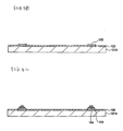
FIG.3C , thebump 104 is formed on theelectrode pads 103 by the wire bonding machine, for example, respectively. Thisbump 104 is formed of the bonding wire that is made of Au. The wire bonding machine forms the bumpmain body 104A bonded to theelectrode pad 103 and theprojection portion 104B projecting from the bumpmain body 104A, by performing successively bonding process of the bonding wire to theelectrode pad 103 and cutting process of the bonding wire after this bonding process. - Then, in steps shown in
FIG.3D , the insulatingfilm 105 made of a resin material is laminated (pasted) on the whole surface of thesubstrate 101A (the passivation layer 102). As a material of the insulatinglayer 105, the elastically deformable soft resin material to which a hardness adjusting material such as a filler called NCF, for example, is hardly added is selected. Also, it is preferable that a thickness should be set to 20 to 50 µm. - The
bumps 104 are embedded in the insulatinglayer 105 in a state that this insulatinglayer 105 is provided. However, there is no necessity that top ends of theprojection portions 104B should necessarily be exposed from the upper surface of the insulatinglayer 105. - Then, a
copper foil 112 is provided on the insulatinglayer 105, and a press-fitting process is applied. Accordingly, the insulatinglayer 105 is also pressed, and a part of theprojection portions 104B of thebumps 104 is exposed from the upper surface of the insulatinglayer 105. - At this time, a thickness of the insulating
layer 105 is selected such that theprojection portions 104B are exposed from the upper surface of the insulatinglayer 105 in the press-fitting process without fail. Also, theprojection portions 104B of thebumps 104 are pressed by thecopper foil 112 in this press-fitting process, and a height of the top end portions are leveled. - In this case, the material of the insulating
layer 105 is not limited to the above NCF, and various insulating material (resin materials) can be employed. For example, a build-up resin (an epoxy resin containing the filler) or a resin material called ACF can be employed as the insulatinglayer 105. Also, the layer formed on the insulatinglayer 105 is not always formed of thecopper foil 112, and a temporary film made of PET can be employed. In addition, a single-sided copper-foil resin film in which a Cu foil is provided to one surface of a resin film can be employed. - After the press-fitting process, the
copper foil 112 is removed by the etching method, for example.FIG.3E shows a state that thecopper foil 112 is removed. As described above, theprojection portions 104B are exposed from the insulatinglayer 105 at the press-fitting process and also their heights are leveled. Therefore, theprojection portions 104B are exposed from the insulatinglayer 105 when thecopper foil 112 is removed. - Then, in steps shown in
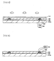
FIG.3F , thestress absorbing layer 120 is laminated (pasted) on the insulatinglayer 105. Thestress absorbing layer 120 is a flat sheet-like member, and is provided in the almost all surface of thebump providing area 135, in which the plurality of solder bumps 110 are provided in the later step, on the insulatinglayer 105. - In the present embodiment, the
stress absorbing layer 120 is formed of the same material as the insulatinglayer 105. That is, the elastically deformable soft resin material to which a hardness adjusting material such as the filler called NCF, for example, is hardly added is employed as thestress absorbing layer 120. Also, a thickness of thestress absorbing layer 120 is equal to the insulatinglayer 105, and is set to 20 to 50 µm. - In this manner, when the material and the thickness of the
stress absorbing layer 120 are set equal to those of the insulatinglayer 105, the same equipment used to form the insulatinglayer 105 can be employed as that used to form thestress absorbing layer 120. Therefore, the process of forming thestress absorbing layer 120 can be simplified, and also simplification of the manufacturing facilities can be attained. - Also, normally the solder bumps 110 serving as the external connection terminals are provided to fan-in from the provision position of the
bumps 104. That is, thebump providing area 135 is positioned on the inner side than the forming positions of thebumps 104 on thesemiconductor chip 101. Hence, the positions in which theprojection portions 104B of thebumps 104 are exposed from the insulatinglayer 105 are positioned on the outside of thestress absorbing layer 120. Therefore, such a situation is never caused that the top end portions of theprojection portions 104B are covered with thestress absorbing layer 120 by forming thestress absorbing layer 120. - In this case, the material of the
stress absorbing layer 120 is not limited to the above NCF. Various materials (insulating materials) can be employed which have an elasticity that can absorb the stress generated between the solder bumps 110 and theconductive pattern 106. For example, a build-up resin (an epoxy resin containing the filler) or a resin material called ACF can be employed as thestress absorbing layer 120. Also, a thickness of thestress absorbing layer 120 is not necessarily set equal to that of the insulatinglayer 105, and the thickness can be adjusted appropriately to absorb the stress generated between the solder bumps 110 and theconductive pattern 106. - In this manner, when the
stress absorbing layer 120 is formed on the insulatinglayer 105, a firstconductive layer 107A is formed on the insulatinglayer 105, thestress absorbing layer 120, and the bumpmain bodies 104A in steps shown inFIG.3G . The firstconductive layer 107A can be formed by the sputter method, which is one type of the vapor deposition method. In this case, the forming method is not limited to this method, and other vapor deposition method such as the CVD method can be employed. - The first
conductive pattern 107 is constructed by forming theCu film 115 on theTi film 114. In order to form the firstconductive pattern 107 on the insulatinglayer 105, firstly theTi film 114 is formed by the sputtering with Ti as a target, and then theCu film 115 is formed by the sputtering with Cu as a target. The processes of forming theTi film 114 and theCu film 115 can be performed successively while using the same sputtering equipment. - Also, in the present embodiment, a thickness of the
Ti film 114 is set to 0.1 µm and a thickness of theCu film 115 is set to 0.1 µm (InFIG.3G to FIG.3I andFIG.4 , for convenience of illustration, theTi film 114 and theCu film 115 are depicted thicker than other layers in an exaggerated way). However, the thickness and the material of theTi film 114 are not limited to the above. For example, an adhesive metal layer such as a Cr film whose thickness is set to 0.035 µm, or the like may be provided in place of theTi film 114. Also, the formation of theTi film 114 can be omitted, and only theCu film 115 can be formed. - In the present embodiment, as described above, the first
conductive layer 107A (theTi film 114, the Cu film 115) is formed by using the sputter method. Therefore, theprojection portions 104B projecting from the insulatinglayer 105 are metallic-bonded to theTi film 114. Also, since theCu film 115 formed on theTi film 114 is formed by using the sputter method, theCu film 115 is metallic-bonded to theTi film 114. - Therefore, the
bumps 104 and the firstconductive layer 107A can be bonded tightly rather than the bonding method using the press-fitting or the conductive paste in the related art. Thus, the electrical and mechanical connectivity between them can be increased. - Then, in steps shown in
FIG.3H to FIG.3J , theconductive pattern 106 connected to thebumps 104 is formed by the electroplating using the firstconductive layer 107A as a power feeding layer (seed layer). As the method of forming theconductive pattern 106, for example, there are so-called subtractive method and semi-additive method. In the present embodiment, an example using the subtractive method will be described. - First, in steps shown in
FIG.3H , a secondconductive layer 108A made of Cu, for example, is formed on the firstconductive layer 107A by the electroplating using the firstconductive layer 107A (theTi film 114, the Cu film 115) as a power feeding layer. Since the firstconductive layer 107A is formed on the insulatinglayer 105 and thestress absorbing layer 120 formed on the insulatinglayer 105, the secondconductive layer 108A is also formed on the whole upper surface of the insulatinglayer 105 and thestress absorbing layer 120. - Then, in steps shown in
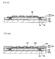
FIG.3I , a mask pattern R1 having opening portions Ra is formed on the secondconductive layer 108A. The mask pattern R1 can be formed by forming a resist layer by a resist coating or a film pasting, and then patterning the resist layer through the photolithography method. - Then, the first
conductive layer 107A and the secondconductive layer 108A are etched while using the mask pattern R1 as a mask. Thus, as shown inFIG.3J , theconductive pattern 106 has the multilayer structure in which the firstconductive pattern 107 and the secondconductive pattern 108 are formed and is connected to thebumps 104. In the present embodiment, a thickness of the firstconductive layer 107A is set to 1 to 2 µm and a thickness of the secondconductive pattern 108 is set to about 10 to 30 µm. But these numerical value are given as an example, and the present invention is not limited to these numerical values. - Upon forming the
conductive pattern 106, the electroplating method can be easily applied by using the firstconductive layer 107A as a power feeding layer. For example, when the power feeding layer (seed layer) is formed by the electroless plating, a process of roughening the surface of the insulating layer (so-called desmear process) is needed and thus the process of forming the plating layer becomes complicated. - In contrast, according to the method of the present embodiment, the desmear process is not needed, and thus the power feeding layer (the first
conductive layer 107A) can be formed easily by a simple method. Therefore, according to the above method, the method of manufacturing the semiconductor device can be made simple and a manufacturing cost can be reduced. - Then, in steps shown in
FIG.3K , as necessary, the solder resist layer (insulating layer) 109 havingopening portions 109A is formed on the insulatinglayer 105 after the process of roughening the surface of the conductive pattern 106 (Cu). A portion of theconductive pattern 106 is exposed from the openingportions 109A. - Then, in steps shown in
FIG.3L , as necessary, thesubstrate 101A is thinned to a predetermined thickness by grinding the back surface of thesubstrate 101A. - Then, in steps shown in
FIG.3M , the solder bumps 110 are formed on theconductive pattern 106 that is exposed from theopening portion 109A. The solder bumps 110 are formed in thebump providing area 135. Therefore, the insulatinglayer 105 and thestress absorbing layer 120 both being formed of elastically deformable material are interposed between the solder bumps 110 and thesemiconductor chip 101. Then, thesubstrate 101A is cut into individual semiconductor chips by the dicing, whereby thesemiconductor device 100 shown inFIG.1A is manufactured. - Meanwhile, in the above manufacturing method, the
conductive pattern 106 is formed by the subtractive method. But theconductive pattern 106 may be formed by the semi-additive method. In this case, for example, after the steps shown inFIG.3A to FIG.3G are performed in the above manufacturing method, the following steps may be performed in place of steps inFIG.3H to FIG.3J . - That is, as shown in
FIG.4 , a mask pattern R2 having opening portions Rb corresponding to the forming positions of theconductive pattern 106 is formed on the firstconductive layer 107A. The mask pattern R2 can be formed by forming a resist layer by a resist coating or a film pasting, and then patterning the resist layer through the photolithography method. - Then, the second conductive pattern is formed on the first
conductive layer 107A, which is exposed from the opening portions Rb, by the electroplating using the firstconductive layer 107A as a power feeding layer (a seed layer). Then, the mask pattern R2 is peeled off, and then the extrapower feeding layer 107A exposed when the mask pattern R2 is peeled off is removed by etching. Thus, theconductive pattern 106 shown inFIG.3J can be formed. - While the present invention has been shown and described with reference to certain exemplary embodiments thereof, other implementations are within the scope of the claims. It will be understood by those skilled in the art that various changes in form and details may be made therein without departing from the spirit and scope of the invention as defined by the appended claims.
- Concretely, instead of the semiconductor substrate, the glass substrate or the multilayered wiring substrate can be employed as the
substrate 101A. Accordingly, exemplary embodiments of the present invention are applicable to various electronic devices using these substrates. - Also, in the above embodiment, the
stress absorbing layer 120 is formed as a single layer structure. The multilayered structure in which a plurality of layers each having the same or different characteristics (elasticity, etc.) are formed may be employed. - According to the present invention, the stress absorbing layer is formed in the bump providing area on the insulating layer, and also the first bumps are formed on the conductive pattern formed on this stress absorbing layer. Therefore, even when a difference of thermal expansion exists between the substrate and the mounting substrate on which the electronic device is mounted, a stress generated due to this difference of thermal expansion can be absorbed by the stress absorbing layer, and such a situation can be prevented that the stress is applied to the connection position between the first bumps and the wiring pattern. As a result, break never occurs in the bonding position between the first bumps and the wiring pattern, and thus mounting reliability can be improved.
This application is based on and claims priority from Japanese Patent Application No.2007-163763, filed on June 21, 2007
Claims (8)
- A method of manufacturing an electronic device in which a plurality of first bumps (110) serving as external connection terminals are formed on a conductive pattern (106), the method comprising:(a) forming a second bump (104) having a projection portion (104A) on an electrode pad (103) formed on a substrate (101);(b) forming an insulating layer (105) on the substrate (101);(c) exposing a portion of the projection portion (104A) from an upper surface of the insulating layer (105);(d) forming a flat stress absorbing layer (120) in a bump providing area (135), in which the first bumps (110) are provided, on the insulating layer;(e) forming a first conductive layer (107) on the insulating layer (105) and the stress absorbing layer (120) and the exposed portion of the projection portion (104A);(f) forming a second conductive layer (108) by an electroplating using the first conductive layer (107) as a power feeding layer;(g) forming the conductive pattern (106) by patterning the second conductive layer (108); and(h) forming the first bumps (110) on the conductive pattern (106) formed on the stress absorbing layer (120).
- The method according to claim 1, wherein the substrate is a semiconductor substrate.
- The method according to claim 1 or 2, wherein the stress absorbing layer is formed of a resin having an elasticity.
- The method according to any one of the preceding claims, wherein the stress absorbing layer is formed of the same material as the insulating layer.
- The method according to any one of the preceding claims, wherein in step (e),
the first conductive layer is formed by a vapor deposition method. - The method according to any one of the preceding claims, wherein in step (a),
the second bump is formed of a bonding wire. - An electronic device, comprising:first bumps (110) serving as external connection terminals;a substrate (101) on which an electrode pad (103) is formed;a second bump (104) formed on the electrode pad (103);an insulating layer (105) formed on the substrate; anda conductive pattern (106) formed on the insulating layer (105) and coupled to the first bumps (110) and the second bump (104); anda stress absorbing layer (120) provided in a bump providing area (135), in which the first bumps (110) are provided, on the insulating layer (105) and over which the first bumps (110) are disposed.
- The electronic device according to claim 7, wherein the substrate is a semiconductor chip.
Applications Claiming Priority (1)
| Application Number | Priority Date | Filing Date | Title |
|---|---|---|---|
| JP2007163763A JP4708399B2 (en) | 2007-06-21 | 2007-06-21 | Electronic device manufacturing method and electronic device |
Publications (3)
| Publication Number | Publication Date |
|---|---|
| EP2006908A2 true EP2006908A2 (en) | 2008-12-24 |
| EP2006908A3 EP2006908A3 (en) | 2009-11-11 |
| EP2006908B1 EP2006908B1 (en) | 2013-08-14 |
Family
ID=39766904
Family Applications (1)
| Application Number | Title | Priority Date | Filing Date |
|---|---|---|---|
| EP08158703.2A Ceased EP2006908B1 (en) | 2007-06-21 | 2008-06-20 | Electronic device and method of manufacturing the same |
Country Status (6)
| Country | Link |
|---|---|
| US (1) | US20090001570A1 (en) |
| EP (1) | EP2006908B1 (en) |
| JP (1) | JP4708399B2 (en) |
| KR (1) | KR20080112987A (en) |
| CN (1) | CN101330026B (en) |
| TW (1) | TW200901412A (en) |
Families Citing this family (17)
| Publication number | Priority date | Publication date | Assignee | Title |
|---|---|---|---|---|
| JP4121542B1 (en) * | 2007-06-18 | 2008-07-23 | 新光電気工業株式会社 | Manufacturing method of electronic device |
| JP4635062B2 (en) | 2008-03-11 | 2011-02-16 | 株式会社東芝 | Manufacturing method of semiconductor device |
| JP5140565B2 (en) * | 2008-11-28 | 2013-02-06 | 三洋電機株式会社 | Device mounting substrate, semiconductor module, and portable device |
| CN101835085A (en) * | 2010-05-10 | 2010-09-15 | 瑞声声学科技(深圳)有限公司 | Manufacturing method of silicon-based condenser microphone |
| CN101848411A (en) * | 2010-06-07 | 2010-09-29 | 瑞声声学科技(深圳)有限公司 | Silica-based condenser microphone and production method thereof |
| JP2012134270A (en) * | 2010-12-21 | 2012-07-12 | Shinko Electric Ind Co Ltd | Semiconductor device and manufacturing method of the same |
| CN103165566B (en) * | 2011-12-19 | 2016-02-24 | 先进封装技术私人有限公司 | The manufacture method of board structure, semiconductor package part and semiconductor package part |
| KR102012935B1 (en) | 2012-06-13 | 2019-08-21 | 삼성전자주식회사 | Electrical interconnection structures and methods for fabricating the same |
| US9041215B2 (en) | 2013-03-12 | 2015-05-26 | Taiwan Semiconductor Manufacturing Company, Ltd. | Single mask package apparatus and method |
| CN103545320B (en) * | 2013-11-11 | 2015-11-25 | 京东方科技集团股份有限公司 | Display base plate and the flexible display apparatus containing this display base plate |
| KR102211741B1 (en) * | 2014-07-21 | 2021-02-03 | 삼성전기주식회사 | Printed circuit board and method of manufacturing the same |
| CN105161474B (en) * | 2015-07-08 | 2019-01-04 | 华进半导体封装先导技术研发中心有限公司 | Fan-out package structure and its production technology |
| CN105161466B (en) * | 2015-07-08 | 2018-04-17 | 华进半导体封装先导技术研发中心有限公司 | High-power component fan-out package structure and production technology |
| DE112017002080T5 (en) | 2016-04-19 | 2019-01-24 | Rohm Co., Ltd. | SEMICONDUCTOR COMPONENT, POWER MODULE AND MANUFACTURING METHOD FOR THE SEMICONDUCTOR COMPONENT |
| WO2018207856A1 (en) | 2017-05-10 | 2018-11-15 | ローム株式会社 | Power semiconductor device and method for producing same |
| CN106960829B (en) * | 2017-05-11 | 2019-07-12 | 北京工业大学 | A kind of structure and preparation method thereof for alleviating chip package stress |
| CN114531774B (en) * | 2022-02-21 | 2025-03-25 | 京东方科技集团股份有限公司 | Flexible circuit board, manufacturing method and display device |
Citations (2)
| Publication number | Priority date | Publication date | Assignee | Title |
|---|---|---|---|---|
| JP2002313985A (en) | 2002-04-05 | 2002-10-25 | Oki Electric Ind Co Ltd | Manufacturing method of chip size package |
| JP2007163763A (en) | 2005-12-13 | 2007-06-28 | Hitachi Cable Ltd | Connection jig for optical connectors |
Family Cites Families (17)
| Publication number | Priority date | Publication date | Assignee | Title |
|---|---|---|---|---|
| JPH0267731A (en) * | 1988-09-02 | 1990-03-07 | Toshiba Corp | Solder bump type semiconductor device and manufacture thereof |
| TW448524B (en) * | 1997-01-17 | 2001-08-01 | Seiko Epson Corp | Electronic component, semiconductor device, manufacturing method therefor, circuit board and electronic equipment |
| JP2000323605A (en) * | 1999-05-10 | 2000-11-24 | Hitachi Ltd | Semiconductor device, manufacture thereof, electronic device using the same |
| KR100298827B1 (en) * | 1999-07-09 | 2001-11-01 | 윤종용 | Method For Manufacturing Wafer Level Chip Scale Packages Using Redistribution Substrate |
| US6770547B1 (en) * | 1999-10-29 | 2004-08-03 | Renesas Technology Corporation | Method for producing a semiconductor device |
| JP2001144204A (en) * | 1999-11-16 | 2001-05-25 | Nec Corp | Semiconductor device and manufacturing method thereof |
| JP3629178B2 (en) * | 2000-02-21 | 2005-03-16 | Necエレクトロニクス株式会社 | Flip chip type semiconductor device and manufacturing method thereof |
| US6638847B1 (en) * | 2000-04-19 | 2003-10-28 | Advanced Interconnect Technology Ltd. | Method of forming lead-free bump interconnections |
| JP2002050716A (en) * | 2000-08-02 | 2002-02-15 | Dainippon Printing Co Ltd | Semiconductor device and manufacturing method thereof |
| JP3640876B2 (en) * | 2000-09-19 | 2005-04-20 | 株式会社ルネサステクノロジ | Semiconductor device and mounting structure of semiconductor device |
| US6433427B1 (en) * | 2001-01-16 | 2002-08-13 | Industrial Technology Research Institute | Wafer level package incorporating dual stress buffer layers for I/O redistribution and method for fabrication |
| JP4361222B2 (en) * | 2001-03-19 | 2009-11-11 | 株式会社フジクラ | Semiconductor package and semiconductor package manufacturing method |
| JP3767398B2 (en) * | 2001-03-19 | 2006-04-19 | カシオ計算機株式会社 | Semiconductor device and manufacturing method thereof |
| JP4173751B2 (en) * | 2003-02-28 | 2008-10-29 | 株式会社ルネサステクノロジ | Semiconductor device |
| US7180185B2 (en) * | 2003-06-13 | 2007-02-20 | Oki Electric Industry Co., Ltd | Semiconductor device with connections for bump electrodes |
| US7452803B2 (en) * | 2004-08-12 | 2008-11-18 | Megica Corporation | Method for fabricating chip structure |
| JP2007088142A (en) * | 2005-09-21 | 2007-04-05 | Fujikura Ltd | Semiconductor device, method for manufacturing the same, and electronic device |
-
2007
- 2007-06-21 JP JP2007163763A patent/JP4708399B2/en active Active
-
2008
- 2008-06-19 US US12/142,053 patent/US20090001570A1/en not_active Abandoned
- 2008-06-19 TW TW097122827A patent/TW200901412A/en unknown
- 2008-06-20 EP EP08158703.2A patent/EP2006908B1/en not_active Ceased
- 2008-06-20 KR KR1020080058433A patent/KR20080112987A/en not_active Withdrawn
- 2008-06-23 CN CN2008101252625A patent/CN101330026B/en not_active Expired - Fee Related
Patent Citations (2)
| Publication number | Priority date | Publication date | Assignee | Title |
|---|---|---|---|---|
| JP2002313985A (en) | 2002-04-05 | 2002-10-25 | Oki Electric Ind Co Ltd | Manufacturing method of chip size package |
| JP2007163763A (en) | 2005-12-13 | 2007-06-28 | Hitachi Cable Ltd | Connection jig for optical connectors |
Also Published As
| Publication number | Publication date |
|---|---|
| CN101330026B (en) | 2011-08-03 |
| KR20080112987A (en) | 2008-12-26 |
| TW200901412A (en) | 2009-01-01 |
| JP4708399B2 (en) | 2011-06-22 |
| CN101330026A (en) | 2008-12-24 |
| EP2006908A3 (en) | 2009-11-11 |
| EP2006908B1 (en) | 2013-08-14 |
| US20090001570A1 (en) | 2009-01-01 |
| JP2009004544A (en) | 2009-01-08 |
Similar Documents
| Publication | Publication Date | Title |
|---|---|---|
| EP2006908B1 (en) | Electronic device and method of manufacturing the same | |
| US7417311B2 (en) | Semiconductor device and method of fabricating the same | |
| KR100540524B1 (en) | Methods for manufacturing electronic component and semiconductor device, semiconductor device, circuit board and electronic equipment | |
| US8350377B2 (en) | Semiconductor device package structure and method for the same | |
| US8294275B2 (en) | Chip package and method for forming the same | |
| KR100371282B1 (en) | Semiconductor device and method of manufacturing the same | |
| JP2001257288A (en) | Flip chip type semiconductor device and manufacturing method thereof | |
| JP3450238B2 (en) | Semiconductor device and manufacturing method thereof | |
| JP2001144204A (en) | Semiconductor device and manufacturing method thereof | |
| CA2272434A1 (en) | Chip scale ball grid array for integrated circuit package | |
| JP2004193497A (en) | Chip size package and manufacturing method thereof | |
| JP2006222164A (en) | Semiconductor device and manufacturing method thereof | |
| US7795127B2 (en) | Electronic device manufacturing method and electronic device | |
| US8766101B2 (en) | Wiring substrate, method for manufacturing wiring substrate, and semiconductor package including wiring substrate | |
| US6955944B2 (en) | Fabrication method for a semiconductor CSP type package | |
| KR101003437B1 (en) | Electronic component mounting structure and manufacturing method | |
| JP4121543B1 (en) | Electronic equipment | |
| EP2065928A2 (en) | Semiconductor device and manufacturing method thereof | |
| US8232639B2 (en) | Semiconductor-device mounted board and method of manufacturing the same | |
| US7915078B2 (en) | Manufacturing method for semiconductor device embedded substrate | |
| JP4214969B2 (en) | Manufacturing method of semiconductor device | |
| KR100501094B1 (en) | Electronic components and semiconductor devices, and methods of manufacturing them | |
| JP2004319656A (en) | Manufacturing method of wafer level CSP | |
| US7985619B2 (en) | Manufacturing method for semiconductor device embedded substrate | |
| CN114429940A (en) | Semiconductor device and method for manufacturing semiconductor device |
Legal Events
| Date | Code | Title | Description |
|---|---|---|---|
| PUAI | Public reference made under article 153(3) epc to a published international application that has entered the european phase |
Free format text: ORIGINAL CODE: 0009012 |
|
| AK | Designated contracting states |
Kind code of ref document: A2 Designated state(s): AT BE BG CH CY CZ DE DK EE ES FI FR GB GR HR HU IE IS IT LI LT LU LV MC MT NL NO PL PT RO SE SI SK TR |
|
| AX | Request for extension of the european patent |
Extension state: AL BA MK RS |
|
| PUAL | Search report despatched |
Free format text: ORIGINAL CODE: 0009013 |
|
| AK | Designated contracting states |
Kind code of ref document: A3 Designated state(s): AT BE BG CH CY CZ DE DK EE ES FI FR GB GR HR HU IE IS IT LI LT LU LV MC MT NL NO PL PT RO SE SI SK TR |
|
| AX | Request for extension of the european patent |
Extension state: AL BA MK RS |
|
| 17P | Request for examination filed |
Effective date: 20100511 |
|
| AKX | Designation fees paid |
Designated state(s): DE |
|
| 17Q | First examination report despatched |
Effective date: 20101229 |
|
| RIC1 | Information provided on ipc code assigned before grant |
Ipc: H01L 21/60 20060101ALI20110922BHEP Ipc: H01L 23/31 20060101AFI20110922BHEP |
|
| GRAP | Despatch of communication of intention to grant a patent |
Free format text: ORIGINAL CODE: EPIDOSNIGR1 |
|
| GRAS | Grant fee paid |
Free format text: ORIGINAL CODE: EPIDOSNIGR3 |
|
| GRAA | (expected) grant |
Free format text: ORIGINAL CODE: 0009210 |
|
| AK | Designated contracting states |
Kind code of ref document: B1 Designated state(s): DE |
|
| REG | Reference to a national code |
Ref country code: DE Ref legal event code: R096 Ref document number: 602008026715 Country of ref document: DE Effective date: 20131010 |
|
| PLBE | No opposition filed within time limit |
Free format text: ORIGINAL CODE: 0009261 |
|
| STAA | Information on the status of an ep patent application or granted ep patent |
Free format text: STATUS: NO OPPOSITION FILED WITHIN TIME LIMIT |
|
| 26N | No opposition filed |
Effective date: 20140515 |
|
| REG | Reference to a national code |
Ref country code: DE Ref legal event code: R097 Ref document number: 602008026715 Country of ref document: DE Effective date: 20140515 |
|
| PGFP | Annual fee paid to national office [announced via postgrant information from national office to epo] |
Ref country code: DE Payment date: 20190604 Year of fee payment: 12 |
|
| REG | Reference to a national code |
Ref country code: DE Ref legal event code: R119 Ref document number: 602008026715 Country of ref document: DE |
|
| PG25 | Lapsed in a contracting state [announced via postgrant information from national office to epo] |
Ref country code: DE Free format text: LAPSE BECAUSE OF NON-PAYMENT OF DUE FEES Effective date: 20210101 |