EP2006722A2 - Optical modulation element - Google Patents
Optical modulation element Download PDFInfo
- Publication number
- EP2006722A2 EP2006722A2 EP07715229A EP07715229A EP2006722A2 EP 2006722 A2 EP2006722 A2 EP 2006722A2 EP 07715229 A EP07715229 A EP 07715229A EP 07715229 A EP07715229 A EP 07715229A EP 2006722 A2 EP2006722 A2 EP 2006722A2
- Authority
- EP
- European Patent Office
- Prior art keywords
- thin substrate
- light
- optical waveguide
- adhesive layer
- modulation device
- Prior art date
- Legal status (The legal status is an assumption and is not a legal conclusion. Google has not performed a legal analysis and makes no representation as to the accuracy of the status listed.)
- Granted
Links
Images
Classifications
-
- G—PHYSICS
- G02—OPTICS
- G02F—OPTICAL DEVICES OR ARRANGEMENTS FOR THE CONTROL OF LIGHT BY MODIFICATION OF THE OPTICAL PROPERTIES OF THE MEDIA OF THE ELEMENTS INVOLVED THEREIN; NON-LINEAR OPTICS; FREQUENCY-CHANGING OF LIGHT; OPTICAL LOGIC ELEMENTS; OPTICAL ANALOGUE/DIGITAL CONVERTERS
- G02F1/00—Devices or arrangements for the control of the intensity, colour, phase, polarisation or direction of light arriving from an independent light source, e.g. switching, gating or modulating; Non-linear optics
- G02F1/01—Devices or arrangements for the control of the intensity, colour, phase, polarisation or direction of light arriving from an independent light source, e.g. switching, gating or modulating; Non-linear optics for the control of the intensity, phase, polarisation or colour
- G02F1/21—Devices or arrangements for the control of the intensity, colour, phase, polarisation or direction of light arriving from an independent light source, e.g. switching, gating or modulating; Non-linear optics for the control of the intensity, phase, polarisation or colour by interference
- G02F1/225—Devices or arrangements for the control of the intensity, colour, phase, polarisation or direction of light arriving from an independent light source, e.g. switching, gating or modulating; Non-linear optics for the control of the intensity, phase, polarisation or colour by interference in an optical waveguide structure
-
- G—PHYSICS
- G02—OPTICS
- G02F—OPTICAL DEVICES OR ARRANGEMENTS FOR THE CONTROL OF LIGHT BY MODIFICATION OF THE OPTICAL PROPERTIES OF THE MEDIA OF THE ELEMENTS INVOLVED THEREIN; NON-LINEAR OPTICS; FREQUENCY-CHANGING OF LIGHT; OPTICAL LOGIC ELEMENTS; OPTICAL ANALOGUE/DIGITAL CONVERTERS
- G02F1/00—Devices or arrangements for the control of the intensity, colour, phase, polarisation or direction of light arriving from an independent light source, e.g. switching, gating or modulating; Non-linear optics
- G02F1/01—Devices or arrangements for the control of the intensity, colour, phase, polarisation or direction of light arriving from an independent light source, e.g. switching, gating or modulating; Non-linear optics for the control of the intensity, phase, polarisation or colour
- G02F1/03—Devices or arrangements for the control of the intensity, colour, phase, polarisation or direction of light arriving from an independent light source, e.g. switching, gating or modulating; Non-linear optics for the control of the intensity, phase, polarisation or colour based on ceramics or electro-optical crystals, e.g. exhibiting Pockels effect or Kerr effect
- G02F1/035—Devices or arrangements for the control of the intensity, colour, phase, polarisation or direction of light arriving from an independent light source, e.g. switching, gating or modulating; Non-linear optics for the control of the intensity, phase, polarisation or colour based on ceramics or electro-optical crystals, e.g. exhibiting Pockels effect or Kerr effect in an optical waveguide structure
-
- G—PHYSICS
- G02—OPTICS
- G02F—OPTICAL DEVICES OR ARRANGEMENTS FOR THE CONTROL OF LIGHT BY MODIFICATION OF THE OPTICAL PROPERTIES OF THE MEDIA OF THE ELEMENTS INVOLVED THEREIN; NON-LINEAR OPTICS; FREQUENCY-CHANGING OF LIGHT; OPTICAL LOGIC ELEMENTS; OPTICAL ANALOGUE/DIGITAL CONVERTERS
- G02F2202/00—Materials and properties
- G02F2202/28—Adhesive materials or arrangements
Definitions
- the present invention relates to a light modulation device, and more particularly, to a light modulation device using a thin film made of material with an electro-optical effect.
- a waveguide type light modulation device where optical waveguides or modulation electrodes are formed on a substrate having an electro-optical effect, has been much used in an optical communication field or an optical measurement field.
- an information transfer amount has a tendency to be increased accompanied by progress of multimedia and thus a widening of a light modulation frequency is demanded.
- an external modulation method by an LN modulator or the like employing LiNbO 3 (hereinafter, referred to as "LN") has been proposed.
- LN LiNbO 3
- a velocity matching between a microwave which is a modulation signal and a light wave and reduction of deriving voltages are required.
- first substrate a substrate with a thickness of below 30 ⁇ m
- second substrate another substrate with a lower permittivity than the first substrate is bonded thereto, to reduce an effective refractive for the microwave for intending to match a velocity between the microwave and the light wave and further to maintain strength of the substrates.
- Patent Document 1 or 2 LiNbO 3 is mainly used for the first substrate, and material with a lower permittivity than LN, such as quartz, glass, alumina or the like is used for the second substrate.
- a temperature drift or a DC drift accompanied by a temperature variation occurs in a combination of such material by a difference of a coefficient of linear expansion therebetween.
- Patent Document 2 discloses that, in order to remove such inconvenience, the bonding of the first substrate and the second substrate is performed by use of an adhesive with a coefficient of linear expansion close to the first substrate.
- the substrate becomes thinner, light emitted or leaked from the optical waveguide, or light and the like incident on other than the optical waveguide from an optical fiber for incidence (hereinafter, such light is referred to as "faint light.") has a strong tendency to be confined within the substrates.
- the substrate is thick (e.g., 500 ⁇ m to 1000 ⁇ m), there are sufficient areas which do not influence the waveguide (e.g., several ⁇ m in depth) and a spatial distribution density of light filled with the faint light (hereinafter, referred to as "faint light density”) becomes lower.
- the faint light has little impact.
- a thickness of the substrate is the same as a distance in a depth direction of the waveguide, since a faint light density propagating in a direction parallel to a surface of the substrate within the substrate becomes higher, the faint light propagates within the substrate to be re-incident on the optical waveguide or to be incident on an optical fiber for output connected to a light modulation device, resulting in deteriorating a S/N ratio of output light.
- Patent Document 2 there is a problem in that, when a surface, which is opposite to the thin substrate, of a adhesive layer of the supplanting plate is smoothed, the faint light emitted to other than the optical waveguide is reflected on the surface of the supplementing plate to be re-incident on the thin substrate, thereby recombining with the optical waveguide.
- the present invention is directed to solve such problems and to provide a light modulation device capable of not only restricting the faint light propagating in the adhesive layer from being re-incident on the thin substrate but also increasing an adhesive strength of the thin substrate and the supplementing plate.
- the invention related to claim 1 is characterized in a light modulation device having a thin substrate made of material with an electro-optical effect and with a thickness of below 20 ⁇ m; an optical waveguide formed on a surface of the thin substrate or the other surface thereof; and a modulation electrode formed on the surface of the thin substrate and for modulating light passing through the optical waveguide, comprising: a supplementing plate adapted to be bonded to the thin substrate via an adhesive layer, wherein a bonding surface of the supplementing plate is formed as a rough surface relative to a bonding surface of the thin substrate.
- the invention related to claim 2 is characterized in that, in the light modulation device according to claim 1, a roughness of the rough surface is over 1/10 of a wavelength of faint light propagating in the adhesive layer.
- the invention related to claim 3 is characterized in a light modulation device having a thin substrate made of material with an electro-optical effect and with a thickness of below 20 ⁇ m; an optical waveguide formed on a surface of the thin substrate or the other surface thereof; and a modulation electrode formed on the surface of the thin substrate and for modulating light passing through the optical waveguide, comprising: a supplementing plate adapted to be bonded to tie thin substrate via an adhesive layer, wherein a bonding surface of the supplementing plate is formed as a concavo-convex structure.
- the invention related to claim 4 is characterized in that, in the light modulation device according to claim 3, a height of a convex of the concavo-convex structure is over 1/10 of a wavelength of faint light propagating in the adhesive layer.
- the invention related two claim 5 is characterized in a light modulation device having a thin substrate made of material with an electro-optical effect and with a thickness of below 20 ⁇ m; an optical waveguide formed on a surface of the thin substrate or the other surface thereof; and a modulation electrode formed on the surface of the thin substrate and for modulating light passing through the optical waveguide, comprising: a supplementing plate adapted to be bonded to the thin substrate via an adhesive layer, wherein a bonding surface of the supplementing plate is formed as a inclined surface which is inclined with respect to a bonding surface of the thin substrate.
- the invention related to claims 6 is characterized in that, in the light modulation device according to anyone of claims 1 to 5, the optical waveguide is set such that a propagation constant of a light wave propagating in the optical waveguide differs partially.
- a light modulation device having a thin substrate made of material with an electro-optical effect and with a thickness of below 20 ⁇ m; an optical waveguide formed on a surface of the thin substrate or the other surface thereof; and a modulation electrode formed on the surface of the thin substrate and for modulating light passing through the optical waveguide, which comprises a supplementing plate adapted to be bonded to the thin substrate via an adhesive layer, wherein a bonding surface of the supplementing plate is formed as a rough surface relative to a bonding surface of the thin substrate, it is possible to scatter faint light incident on the adhesive layer from the thin substrate on the rough surface of the bonding surface of the supplementing plate, to restrict the faint light from being re-incident on the thin substrate from the adhesive layer. Furthermore, since the bonding surface of the supplementing plate is formed as the rough surface, a contact area with the adhesive layer can be increased, to increase an adhesive strength of the thin substrate and the supplementing plate.
- a roughness of the rough surface is over 1/10 of a wavelength of faint light propagating in the adhesive layer, the faint light can be scattered on the bonding surface of the supplementing plate effectively.
- a light modulation device having a thin substrate made of material with an electro-optical effect and with a thickness of below 20 ⁇ m; an optical waveguide formed on a surface of the thin substrate or the other surface thereof; and a modulation electrode formed on the surface of the thin substrate and for modulating light passing through the optical waveguide, which comprises supplementing plate adapted to be bonded to the thin substrate via an adhesive layer, wherein a bonding surface of the supplementing plate is formed as a concave-convex structure, it is possible to scatter faint light incident on the adhesive layer from the thin substrate on the concavo-convex structure to restrict the faint light from being re-incident on the thin substrate from the adhesive layer.
- the bonding surface of the supplementing plate is formed as the concavo-convex structure, a contact area with the adhesive layer can be increased, to increase an adhesive strength of the thin substrate and the supplementing plate.
- a height of a convex of the concavo-convex structure is over 1/10 of a wavelength of faint light propagating in the adhesive layer, the faint light can be scattered on the bonding surface of the supplementing plate effectively.
- a light modulation device having a thin substrate made of material with an electro-optical effect and with a thickness of below 20 ⁇ m; an optical waveguide formed on a surface of the thin substrate or the other surface thereof; and a modulation electrode formed on the surface of the thin substrate and for modulating light passing through the optical waveguide, which comprises a supplementing plate adapted to be bonded to the thin substrate via an adhesive layer, wherein a bonding surface of the supplementing plate is formed as a inclined surface which is inclined with respect to a bonding surface of the thin substrate, faint light incident on the adhesive layer from the thin substrate is reflected on the inclined surface to be changed towards other than thin substrate in a direction thereof, thereby restricting the faint light from being re-incident on the thin substrate or the optical waveguide from the adhesive layer.
- the bonding surface of the supplementing plate is formed as the inclined surface, a contact area with the adhesive layer can be increased, to increase an adhesive strength of the thin substrate and the supplementing plate.
- the optical waveguide is set such that a propagation constant of a light wave propagating in the optical waveguide differs partially, the effect of removing the faint light from the supplementing plate together with the effect of preventing the recombination of the faint light by adjustment of the propagation constant can prevent the faint light from recombining with the optical waveguide more effectively.
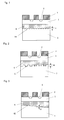
- Fig. 1 illustrates an embodiment 1 related to a light modulation device of the present invention.
- Fig. 1 is a sectional view of the light modulation device, which includes a thin substrate 1 with a thickness of below 20 ⁇ m and made of material with an electro-optical effect, an optical waveguide 2 formed on a surface of the thin substrate, and a modulation electrode 3 for modulating light passing through the optical waveguide.
- the optical waveguide 2 may be formed on the other surface of the thin substrate 1.
- the thin substrate 1 is bonded to a supplementing plate via an adhesive 4.
- the optical waveguide 2 may be formed by diffusing Ti or the like on a surface of the substrate, using a thermal diffusion method or a proton exchanging method.
- the optical waveguide may be configured by forming a ridge on the surface of the thin substrate 1 fitting to a shape of the optical waveguide.
- the modulation electrode 3 such as a signal electrode or a ground electrode may be formed by formation of electrode pattern of Ti/Au, a gold-plate method and the like.
- a buffer layer (not shown) of a dielectric such as SiO 2 may be provided on the surface of the substrate after formation of the optical waveguide, to form the modulation electrode on the buffer layer.
- Patent Document 4 Japanese Patent Application Laid-Open No. H6-289341
- lithium niobate lithium tantalize, PLZT (lead zirconate titanate), quartz-based material, and a combination thereof are available.
- the lithium niobate (LN) crystal with high electro-optical effect is employed suitably.
- the above-described optical waveguide is formed on a substrate with a thickness of several hundreds ⁇ m, and the other surface of the substrate is grinded to create a thin substrate with a thickness of below 20 ⁇ m.
- the modulation electrode is formed on the surface of the thin substrate,
- the other surface of the substrate may be grinded after formation of the optical waveguide or the modulation electrode.
- material used for the supplementing plate 5 various kinds of material are available, for example, in addition to use of material identical to the thin substrate, material with a lower permittivity than the thin substrate, such as quartz, glass, alumina and so on may be used, or material with a crystalline orientation different from the thin substrate may be used like that disclosed in Patent Document 4.
- selection of material with coefficient of linear expansion identical to the thin substrate is preferably in stabilizing a modulation characteristic of the light modulation device relative to a temperature variation. If it is difficult to select material identical thereto, an adhesive for bonding the thin substrate and the supplementing plate is selected as material with a coefficient of linear expansion identical to the thin substrate as disclosed in patent document2.
- various kinds of adhesive material for example, an epoxy based adhesive, a thermosetting adhesive, an ultraviolet thermosetting adhesive, solder glass, or, a thermosetting, a photo curable or a light-increasing-viscosity resin adhesive sheet or the like may be used as the adhesive 4.
- a main object of the present invention is to prevent a light wave incident on the adhesive layer from the thin substrate 1 from being incident on the thin substrate back to recombine with the optical waveguide and so on.
- a bonding surface where the supplementing plate is bonded to the thin substrate 1 is formed as a rough surface 10 compared with a bonding surface (a lower surface of the thin substrate 1 in Fig. 1 ) of the thin substrate 1, as shown in Fig. 1 .
- the formation of the rough surface 10 scatters the faint light in the adhesive layer on the rough surface to restrict the faint light from being re-incident on the thin substrate 1.
- the bonding surface of the supplementing plate is formed as the rough surface, a contact area with the adhesive layer can be increased, to increase an adhesive strength of the thin substrate and the supplementing plate.
- the rough surface extends in a transverse direction as well as in a direction vertical to a sectional surface in Fig. 1 .
- a roughness d1 of the corresponding rough surface preferably has a value of over 1/10 ( ⁇ /10) relative to a wavelength ⁇ of the faint light propagating in the adhesive layer. If the roughness of the rough surface is lower than ⁇ / 10, the faint light cannot be scattered effectively.
- Fig. 2 is a diagram to illustrate the embodiment 2 of the light modulation device, in which like reference numerals are used for like elements in Fig. 1 .
- a characteristic of the embodiment 2 is that a bounding surface where the supplementing plate 5 is bonded to the thin substrate 1 is formed as a concavo-convex structure 11.
- the formation of the concavo-convex structure 11 scatters the faint light in the adhesive layer on the concavo-convex structure to restrict the faint light from being re-incident on the thin substrate 1.
- the bonding surface of the supplementing plate is formed as the concavo-convex structure, a contact area with the adhesive layer can be increased, to increase an adhesive strength of the thin substrate and the supplementing plate.
- the concavo-convex structure extends in a transverse direction as well as in a direction vertical to a sectional surface in Fig. 2 .
- a height d2 of the convex of the corresponding concavo-convex structure 11 preferably has a value of over 1/10 ( ⁇ /10) relative to a wavelength ⁇ of the faint light propagating in the adhesive layer. If the height of the convex is lower than ⁇ /10, the faint light cannot be scattered effectively.
- Fig. 3 is a diagram to illustrate the embodiment 3 of the light modulation device, in which like reference numerals are used for live elements in Figs. 1 and 2 .
- a characteristic of the embodiment 3 is that a bonding surface where the supplementing plate 5 is bonded to the thin substrate 1 is formed as an inclined surface 12 which is inclined with respect to the thin substrate 1, particularly, a bonding surface (a lower surface of the thin substrate 1 in Fig. 3 ) of the thin substrate 1.
- the faint light in the adhesive layer is reflected on the inclined surface 12 to be changed towards other than thin substrate 1 in a direction thereof, thereby restricting the faint light from being re-incident on the thin substrate 1.
- the bonding surface of the supplementing plate is formed as the inclined surface, a contact area with the adhesive layer can be increased, to increase an adhesive strength of the thin substrate and the supplementing plate.
- the shape of the inclined surface 12 is represented to be inclined by an inclined angle ⁇ with respect to the thin substrate 1 within a plane vertical to a propagation direction of the light wave in the optical waveguide 2 in Fig. 3
- the present invention is not limited thereto, but it may be configured so that the inclined surface is inclined with respect to the thin substrate 1 within a plane parallel to a propagation direction of the light wave in the optical waveguide.
- the inclined surface 12 which is inclined in a predetermined direction only with respect to the bonding surface of the thin substrate 1 is possible as shown in Fig. 3 as well as a mountain-shape inclined surface which is lowered in a height thereof as goes to left and right from the center of Fig. 3 is possible.
- a value of the inclined angle 5 of the inclined surface 12 may be set to any value, if the value is in a range where most of the faint light reflected on the bonding surface of the supplementing plate is not incident on the thin substrate 1 or the optical waveguide 2.
- the shape of the bonding surface of the supplementing plate 5 is largely different from the shape of the bonding surface of the thin substrate 1 which is bonded thereto via the same adhesive layer. For this reason, when the supplementing plate 5 is transformed by a thermal expansion, a thermal stress from the supplementing plate 5 may be in danger of local concentration without uniform application to the thin substrate 1. Such concentration of the thermal stress is a cause to deteriorate optical characteristics of the light modulation device. Therefore, a thickness of the adhesive layer is preferably over 10 ⁇ m in order to mitigate the thermal stress from the supplementing plate 5.
- the optical waveguide is designed and adjusted so that a propagation constant of the light wave propagating in the optical waveguide differs partially, to restrict recombination of the faint light and the optical waveguide as disclosed in Patent Document 5.
- the effect of removing the faint light from the supplementing plate according to the embodiments 1 to 3 together with the effect of preventing the recombination of the faint light by adjustment of the propagation constant can prevent the faint light from recombining with the optical waveguide more effectively.
- Patent Document 5 Japanese Patent Application No. 2005-104307 (Application date: March 31, 2005 )
- a light modulation device capable of not only preventing faint light propagating in an adhesive layer from being re-incident on a thin substrate but also increasing an adhesive strength between the thin substrate and a supplementing plate.
Landscapes
- Physics & Mathematics (AREA)
- Nonlinear Science (AREA)
- General Physics & Mathematics (AREA)
- Optics & Photonics (AREA)
- Chemical & Material Sciences (AREA)
- Engineering & Computer Science (AREA)
- Ceramic Engineering (AREA)
- Crystallography & Structural Chemistry (AREA)
- Optical Modulation, Optical Deflection, Nonlinear Optics, Optical Demodulation, Optical Logic Elements (AREA)
Abstract
Description
- The present invention relates to a light modulation device, and more particularly, to a light modulation device using a thin film made of material with an electro-optical effect.
- Conventionally, a waveguide type light modulation device where optical waveguides or modulation electrodes are formed on a substrate having an electro-optical effect, has been much used in an optical communication field or an optical measurement field.
Specially, an information transfer amount has a tendency to be increased accompanied by progress of multimedia and thus a widening of a light modulation frequency is demanded. As means for realizing the widening, an external modulation method by an LN modulator or the like employing LiNbO3 (hereinafter, referred to as "LN") has been proposed. However, in order to realize the widening of the LN modulator, a velocity matching between a microwave which is a modulation signal and a light wave and reduction of deriving voltages are required. - As means for solving such problems, it has been known conventionally that making a thickness of a substrate thin is intended to satisfy a velocity matching condition of a microwave and a light wave as well as to reduce driving voltages.
In thehollowing Patent Document - Patent Document 1: Japanese Patent Application Laid-Open No.
S64-13121 - Patent Document 2: Japanese Patent Application Laid-Open No.
2003-215519 - In the
Patent Document Patent Document 2 discloses that, in order to remove such inconvenience, the bonding of the first substrate and the second substrate is performed by use of an adhesive with a coefficient of linear expansion close to the first substrate. - However, comparing a modulator using the LN substrate which has been manufactured conventionally with a modulator to make the LN substrate thin, as the substrate becomes thinner, light emitted or leaked from the optical waveguide, or light and the like incident on other than the optical waveguide from an optical fiber for incidence (hereinafter, such light is referred to as "faint light.") has a strong tendency to be confined within the substrates. In the conventional LN substrate, since the substrate is thick (e.g., 500µm to 1000µm), there are sufficient areas which do not influence the waveguide (e.g., several µm in depth) and a spatial distribution density of light filled with the faint light (hereinafter, referred to as "faint light density") becomes lower. As a result, the faint light has little impact. However, when a thickness of the substrate is the same as a distance in a depth direction of the waveguide, since a faint light density propagating in a direction parallel to a surface of the substrate within the substrate becomes higher, the faint light propagates within the substrate to be re-incident on the optical waveguide or to be incident on an optical fiber for output connected to a light modulation device, resulting in deteriorating a S/N ratio of output light.
- In addition, when a thin substrate is used for a light modulation device, since the thin substrate cannot give a sufficient strength, the thin substrate which is the first substrate and the second substrate are required to be bonded by a supplementing plate by use of an adhesive. In this case, when a refractive of the adhesive is lower than that of the thin substrate, the confinement of the faint light is more outstanding. For this reason, this applicant has proposed in
Patent Document 3 that a light absorbing portion, a high refractive portion, a light guide portion or a concave portion is formed in an area excluding the optical waveguide and a periphery thereof in the thin substrate, to remove the faint light within the thin substrate. - Patent Document 3: Japanese Patent Application No.
2005-96447 (Application Date: March 29, 2005 - However, like
Patent Document 2, there is a problem in that, when a surface, which is opposite to the thin substrate, of a adhesive layer of the supplanting plate is smoothed, the faint light emitted to other than the optical waveguide is reflected on the surface of the supplementing plate to be re-incident on the thin substrate, thereby recombining with the optical waveguide. - The present invention is directed to solve such problems and to provide a light modulation device capable of not only restricting the faint light propagating in the adhesive layer from being re-incident on the thin substrate but also increasing an adhesive strength of the thin substrate and the supplementing plate.
- For solving such problems, the invention related to
claim 1 is characterized in a light modulation device having a thin substrate made of material with an electro-optical effect and with a thickness of below 20µm; an optical waveguide formed on a surface of the thin substrate or the other surface thereof; and a modulation electrode formed on the surface of the thin substrate and for modulating light passing through the optical waveguide, comprising: a supplementing plate adapted to be bonded to the thin substrate via an adhesive layer, wherein a bonding surface of the supplementing plate is formed as a rough surface relative to a bonding surface of the thin substrate. - The invention related to
claim 2 is characterized in that, in the light modulation device according toclaim 1, a roughness of the rough surface is over 1/10 of a wavelength of faint light propagating in the adhesive layer. - The invention related to
claim 3 is characterized in a light modulation device having a thin substrate made of material with an electro-optical effect and with a thickness of below 20 µm; an optical waveguide formed on a surface of the thin substrate or the other surface thereof; and a modulation electrode formed on the surface of the thin substrate and for modulating light passing through the optical waveguide, comprising: a supplementing plate adapted to be bonded to tie thin substrate via an adhesive layer, wherein a bonding surface of the supplementing plate is formed as a concavo-convex structure. - The invention related to
claim 4 is characterized in that, in the light modulation device according toclaim 3, a height of a convex of the concavo-convex structure is over 1/10 of a wavelength of faint light propagating in the adhesive layer. - The invention related two
claim 5 is characterized in a light modulation device having a thin substrate made of material with an electro-optical effect and with a thickness of below 20 µm; an optical waveguide formed on a surface of the thin substrate or the other surface thereof; and a modulation electrode formed on the surface of the thin substrate and for modulating light passing through the optical waveguide, comprising: a supplementing plate adapted to be bonded to the thin substrate via an adhesive layer, wherein a bonding surface of the supplementing plate is formed as a inclined surface which is inclined with respect to a bonding surface of the thin substrate. - The invention related to claims 6 is characterized in that, in the light modulation device according to anyone of
claims 1 to 5, the optical waveguide is set such that a propagation constant of a light wave propagating in the optical waveguide differs partially. - According to the invention related to
claim 1, since, in a light modulation device having a thin substrate made of material with an electro-optical effect and with a thickness of below 20µm; an optical waveguide formed on a surface of the thin substrate or the other surface thereof; and a modulation electrode formed on the surface of the thin substrate and for modulating light passing through the optical waveguide, which comprises a supplementing plate adapted to be bonded to the thin substrate via an adhesive layer, wherein a bonding surface of the supplementing plate is formed as a rough surface relative to a bonding surface of the thin substrate, it is possible to scatter faint light incident on the adhesive layer from the thin substrate on the rough surface of the bonding surface of the supplementing plate, to restrict the faint light from being re-incident on the thin substrate from the adhesive layer. Furthermore, since the bonding surface of the supplementing plate is formed as the rough surface, a contact area with the adhesive layer can be increased, to increase an adhesive strength of the thin substrate and the supplementing plate. - According to the invention related to
claim 2, since a roughness of the rough surface is over 1/10 of a wavelength of faint light propagating in the adhesive layer, the faint light can be scattered on the bonding surface of the supplementing plate effectively. - According to the invention related to
claims 3, since, in a light modulation device having a thin substrate made of material with an electro-optical effect and with a thickness of below 20µm; an optical waveguide formed on a surface of the thin substrate or the other surface thereof; and a modulation electrode formed on the surface of the thin substrate and for modulating light passing through the optical waveguide, which comprises supplementing plate adapted to be bonded to the thin substrate via an adhesive layer, wherein a bonding surface of the supplementing plate is formed as a concave-convex structure, it is possible to scatter faint light incident on the adhesive layer from the thin substrate on the concavo-convex structure to restrict the faint light from being re-incident on the thin substrate from the adhesive layer. In addition, since the bonding surface of the supplementing plate is formed as the concavo-convex structure, a contact area with the adhesive layer can be increased, to increase an adhesive strength of the thin substrate and the supplementing plate. - According to the invention related to
claim 4, since a height of a convex of the concavo-convex structure is over 1/10 of a wavelength of faint light propagating in the adhesive layer, the faint light can be scattered on the bonding surface of the supplementing plate effectively. - According to the invention related to
claim 5, since, in a light modulation device having a thin substrate made of material with an electro-optical effect and with a thickness of below 20µm; an optical waveguide formed on a surface of the thin substrate or the other surface thereof; and a modulation electrode formed on the surface of the thin substrate and for modulating light passing through the optical waveguide, which comprises a supplementing plate adapted to be bonded to the thin substrate via an adhesive layer, wherein a bonding surface of the supplementing plate is formed as a inclined surface which is inclined with respect to a bonding surface of the thin substrate, faint light incident on the adhesive layer from the thin substrate is reflected on the inclined surface to be changed towards other than thin substrate in a direction thereof, thereby restricting the faint light from being re-incident on the thin substrate or the optical waveguide from the adhesive layer.
In addition, since the bonding surface of the supplementing plate is formed as the inclined surface, a contact area with the adhesive layer can be increased, to increase an adhesive strength of the thin substrate and the supplementing plate. - According to the invention related to claim 6, since the optical waveguide is set such that a propagation constant of a light wave propagating in the optical waveguide differs partially, the effect of removing the faint light from the supplementing plate together with the effect of preventing the recombination of the faint light by adjustment of the propagation constant can prevent the faint light from recombining with the optical waveguide more effectively.
-
-
Fig. 1 is a sectional view to illustrate an embodiment related to a light modulation device of the present invention; -
Fig. 2 is a sectional view to illustrate anembodiment 2 related to a light modulation device of the present invention; and -
Fig. 3 is a sectional view to illustrate anembodiment 3 related to a light modulation device of the present invention. -
- 1:
- THIN SUBSTRATE
- 2:
- OPTICAL WAVEGUIDE
- 3:
- MODULATION ELECTRODE
- 4:
- ADHESIVE LAYER
- 5:
- SUPPLEMENTING PLATE
- 10:
- ROUGH SURFACE
- 11:
- CONCAVO-CONVEX STRUCTURE
- 12:
- INCLINED SURFACE
- Hereinafter, embodiments of the present invention will be described using suitable examples.
Fig. 1 illustrates anembodiment 1 related to a light modulation device of the present invention.Fig. 1 is a sectional view of the light modulation device, which includes athin substrate 1 with a thickness of below 20 µm and made of material with an electro-optical effect, anoptical waveguide 2 formed on a surface of the thin substrate, and amodulation electrode 3 for modulating light passing through the optical waveguide. In addition, theoptical waveguide 2 may be formed on the other surface of thethin substrate 1.
Furthermore, thethin substrate 1 is bonded to a supplementing plate via anadhesive 4. - The
optical waveguide 2 may be formed by diffusing Ti or the like on a surface of the substrate, using a thermal diffusion method or a proton exchanging method. In addition, like that disclosed inPatent Document 4, the optical waveguide may be configured by forming a ridge on the surface of thethin substrate 1 fitting to a shape of the optical waveguide.
Themodulation electrode 3 such as a signal electrode or a ground electrode may be formed by formation of electrode pattern of Ti/Au, a gold-plate method and the like. Moreover, if necessary, a buffer layer (not shown) of a dielectric such as SiO2 may be provided on the surface of the substrate after formation of the optical waveguide, to form the modulation electrode on the buffer layer.
Patent Document 4: Japanese Patent Application Laid-Open No.H6-289341 - As material with an electro-optical effect, for example, lithium niobate, lithium tantalize, PLZT (lead zirconate titanate), quartz-based material, and a combination thereof are available. In particular, the lithium niobate (LN) crystal with high electro-optical effect is employed suitably.
- According to a method of manufacturing the
thin substrate 1 including the light modulation device, the above-described optical waveguide is formed on a substrate with a thickness of several hundreds µm, and the other surface of the substrate is grinded to create a thin substrate with a thickness of below 20µm. Then, the modulation electrode is formed on the surface of the thin substrate, In addition, the other surface of the substrate may be grinded after formation of the optical waveguide or the modulation electrode. Further, since the thin substrate is in danger of destruction due to a thermal impact upon formation of the optical waveguide or a mechanical impact according to handling of the thin substrate upon various processes, a process where such thermal or mechanical impact is applied thereto easily is preferably performed before making the substrate thin by grinding. - As material used for the supplementing
plate 5, various kinds of material are available, for example, in addition to use of material identical to the thin substrate, material with a lower permittivity than the thin substrate, such as quartz, glass, alumina and so on may be used, or material with a crystalline orientation different from the thin substrate may be used like that disclosed inPatent Document 4. However, selection of material with coefficient of linear expansion identical to the thin substrate is preferably in stabilizing a modulation characteristic of the light modulation device relative to a temperature variation. If it is difficult to select material identical thereto, an adhesive for bonding the thin substrate and the supplementing plate is selected as material with a coefficient of linear expansion identical to the thin substrate as disclosed in patent document2. - For the bonding of the
thin substrate 1 and the supplementingplate 5, various kinds of adhesive material, for example, an epoxy based adhesive, a thermosetting adhesive, an ultraviolet thermosetting adhesive, solder glass, or, a thermosetting, a photo curable or a light-increasing-viscosity resin adhesive sheet or the like may be used as the adhesive 4. - In the light modulation device as shown in
Fig. 1 , faint light occurs in the thin substrate other than the optical waveguide from a light splitter or a light summer of the optical waveguide formed in the thin substrate, or from a bonding portion of an optical fiber for incidence and the light modulation device. In addition, when a thickness of the thin substrate is thin, and, in particular, the thickness thereof is set to below 20µm, a problem is easy to happen that the faint light propagates in the thin substrate to be incident on the optical waveguide or an optical fiber for output. Especially, a main object of the present invention is to prevent a light wave incident on the adhesive layer from thethin substrate 1 from being incident on the thin substrate back to recombine with the optical waveguide and so on. - In order to prevent the light wave propagating in the
adhesive layer 4 from being re-incident on thethin substrate 1, in the light modulation device of the present invention, a bonding surface where the supplementing plate is bonded to thethin substrate 1 is formed as arough surface 10 compared with a bonding surface (a lower surface of thethin substrate 1 inFig. 1 ) of thethin substrate 1, as shown inFig. 1 . The formation of therough surface 10 scatters the faint light in the adhesive layer on the rough surface to restrict the faint light from being re-incident on thethin substrate 1. Furthermore, since the bonding surface of the supplementing plate is formed as the rough surface, a contact area with the adhesive layer can be increased, to increase an adhesive strength of the thin substrate and the supplementing plate.
In addition, the rough surface extends in a transverse direction as well as in a direction vertical to a sectional surface inFig. 1 . - Since the
rough surface 10 is required to serve as a scattering surface for the faint light, a roughness d1 of the corresponding rough surface preferably has a value of over 1/10 (λ/10) relative to a wavelength λ of the faint light propagating in the adhesive layer.
If the roughness of the rough surface is lower than λ / 10, the faint light cannot be scattered effectively. - Subsequently, an
embodiment 2 related to the light modulation device of the present invention will be described.
Fig. 2 is a diagram to illustrate theembodiment 2 of the light modulation device, in which like reference numerals are used for like elements inFig. 1 .
A characteristic of theembodiment 2 is that a bounding surface where the supplementingplate 5 is bonded to thethin substrate 1 is formed as a concavo-convex structure 11.
The formation of the concavo-convex structure 11 scatters the faint light in the adhesive layer on the concavo-convex structure to restrict the faint light from being re-incident on thethin substrate 1. In addition, since the bonding surface of the supplementing plate is formed as the concavo-convex structure, a contact area with the adhesive layer can be increased, to increase an adhesive strength of the thin substrate and the supplementing plate.
In addition, the concavo-convex structure extends in a transverse direction as well as in a direction vertical to a sectional surface inFig. 2 . - Since the concavo-
convex structure 11 is also required to serve as a scattering surface for the faint light like therough surface 10 inFig. 1 , a height d2 of the convex of the corresponding concavo-convex structure 11 preferably has a value of over 1/10 (λ/10) relative to a wavelength λ of the faint light propagating in the adhesive layer.
If the height of the convex is lower than λ/10, the faint light cannot be scattered effectively. - Successively, an
embodiment 3 related to the light modulation device of the present invention will be described.
Fig. 3 is a diagram to illustrate theembodiment 3 of the light modulation device, in which like reference numerals are used for live elements inFigs. 1 and 2 .
A characteristic of theembodiment 3 is that a bonding surface where the supplementingplate 5 is bonded to thethin substrate 1 is formed as aninclined surface 12 which is inclined with respect to thethin substrate 1, particularly, a bonding surface (a lower surface of thethin substrate 1 inFig. 3 ) of thethin substrate 1.
By the formation of theinclined surface 12, the faint light in the adhesive layer is reflected on theinclined surface 12 to be changed towards other thanthin substrate 1 in a direction thereof, thereby restricting the faint light from being re-incident on thethin substrate 1.
In addition, since the bonding surface of the supplementing plate is formed as the inclined surface, a contact area with the adhesive layer can be increased, to increase an adhesive strength of the thin substrate and the supplementing plate. - Although the shape of the
inclined surface 12 is represented to be inclined by an inclined angle δ with respect to thethin substrate 1 within a plane vertical to a propagation direction of the light wave in theoptical waveguide 2 inFig. 3 , the present invention is not limited thereto, but it may be configured so that the inclined surface is inclined with respect to thethin substrate 1 within a plane parallel to a propagation direction of the light wave in the optical waveguide.
In addition, theinclined surface 12 which is inclined in a predetermined direction only with respect to the bonding surface of thethin substrate 1 is possible as shown inFig. 3 as well as a mountain-shape inclined surface which is lowered in a height thereof as goes to left and right from the center ofFig. 3 is possible. - A value of the
inclined angle 5 of theinclined surface 12 may be set to any value, if the value is in a range where most of the faint light reflected on the bonding surface of the supplementing plate is not incident on thethin substrate 1 or theoptical waveguide 2. - As illustrated in the
embodiments 1 to 3 related to the light modulation device of the present invention, the shape of the bonding surface of the supplementingplate 5 is largely different from the shape of the bonding surface of thethin substrate 1 which is bonded thereto via the same adhesive layer. For this reason, when the supplementingplate 5 is transformed by a thermal expansion, a thermal stress from the supplementingplate 5 may be in danger of local concentration without uniform application to thethin substrate 1. Such concentration of the thermal stress is a cause to deteriorate optical characteristics of the light modulation device.
Therefore, a thickness of the adhesive layer is preferably over 10µm in order to mitigate the thermal stress from the supplementingplate 5. - In addition, in the light modulation device of the present invention, even if the faint light is re-incident on the thin substrate from the adhesive layer, the optical waveguide is designed and adjusted so that a propagation constant of the light wave propagating in the optical waveguide differs partially, to restrict recombination of the faint light and the optical waveguide as disclosed in
Patent Document 5. In this way, the effect of removing the faint light from the supplementing plate according to theembodiments 1 to 3 together with the effect of preventing the recombination of the faint light by adjustment of the propagation constant can prevent the faint light from recombining with the optical waveguide more effectively.
As a method of adjusting the propagation constant, there is a method of adjusting a width of the optical waveguide or a method of diffusing or loading material for changing a propagation constant, for example, MgO, SiO2, TiO2 or ZnO on the optical waveguide or a periphery thereof, and this changes a refractive of the optical waveguide.
Patent Document 5: Japanese Patent Application No.2005-104307 (Application date: March 31, 2005 - As described above, according to the present invention, it is possible to provide a light modulation device capable of not only preventing faint light propagating in an adhesive layer from being re-incident on a thin substrate but also increasing an adhesive strength between the thin substrate and a supplementing plate.
Claims (6)
- A light modulation device having a thin substrate made of material with an electro-optical effect and with a thickness of below 20µm; an optical waveguide formed on a surface of the thin substrate or the other surface thereof; and a modulation electrode formed on the surface of the thin substrate and for modulating light passing through the optical waveguide, comprising:a supplementing plate adapted to be bonded to the thin substrate via an adhesive layer,wherein a bonding surface of the supplementing plate is formed as a rough surface relative to a bonding surface of the thin substrate.
- The light modulation device according to claim 1, wherein a roughness of the rough surface is over 1/10 of a wavelength of faint light propagating in the adhesive layer.
- A light modulation device having a thin substrate made of material with an electro-optical effect and with a thickness of below 20µm; an optical waveguide formed on a surface of the thin substrate or the other surface thereof; and a modulation electrode formed on the surface of the thin substrate and for modulating light passing through the optical waveguide, comprising:a supplementing plate adapted to be bonded to the thin substrate via an adhesive layer,wherein a bonding surface of the supplementing plate is formed as a concavo-convex structure.
- The light modulation device according to claim 3, wherein a height of a convex of the concavo-convex structure is over 1/10 of a wavelength of faint light propagating in the adhesive layer.
- A light modulation device having a thin substrate made of material with an electro-optical effect and with a thickness of below 20µm; an optical waveguide formed on a surface of the thin substrate or the other surface thereof; and a modulation electrode formed on the surface of the thin substrate and for modulating light passing through the optical waveguide, comprising:a supplementing plate adapted to be bonded to the thin substrate via an adhesive layer,wherein a bonding surface of the supplementing plate is formed as an inclined surface which is inclined with respect to a bonding surface of the thin substrate.
- The light modulation device according to any one of claims 1 to 5, wherein the optical waveguide is set such that a propagation constant of a light wave propagating in the optical waveguide differs partially.
Applications Claiming Priority (2)
| Application Number | Priority Date | Filing Date | Title |
|---|---|---|---|
| JP2006093098A JP4847177B2 (en) | 2006-03-30 | 2006-03-30 | Light modulation element |
| PCT/JP2007/054261 WO2007122877A1 (en) | 2006-03-30 | 2007-03-06 | Optical modulation element |
Publications (5)
| Publication Number | Publication Date |
|---|---|
| EP2006722A2 true EP2006722A2 (en) | 2008-12-24 |
| EP2006722A4 EP2006722A4 (en) | 2009-04-08 |
| EP2006722A9 EP2006722A9 (en) | 2009-07-15 |
| EP2006722B1 EP2006722B1 (en) | 2011-01-05 |
| EP2006722B9 EP2006722B9 (en) | 2011-06-15 |
Family
ID=38624791
Family Applications (1)
| Application Number | Title | Priority Date | Filing Date |
|---|---|---|---|
| EP07715229A Not-in-force EP2006722B9 (en) | 2006-03-30 | 2007-03-06 | Optical modulation element |
Country Status (6)
| Country | Link |
|---|---|
| US (1) | US8031983B2 (en) |
| EP (1) | EP2006722B9 (en) |
| JP (1) | JP4847177B2 (en) |
| CN (1) | CN101416098B (en) |
| DE (1) | DE602007011741D1 (en) |
| WO (1) | WO2007122877A1 (en) |
Families Citing this family (18)
| Publication number | Priority date | Publication date | Assignee | Title |
|---|---|---|---|---|
| JP4847177B2 (en) * | 2006-03-30 | 2011-12-28 | 住友大阪セメント株式会社 | Light modulation element |
| JP4110182B2 (en) * | 2006-09-30 | 2008-07-02 | 住友大阪セメント株式会社 | Light control element |
| JP4388987B2 (en) * | 2008-03-31 | 2009-12-24 | 住友大阪セメント株式会社 | Mach-Zehnder waveguide type optical modulator |
| JP4954958B2 (en) * | 2008-09-30 | 2012-06-20 | 住友大阪セメント株式会社 | Optical waveguide device |
| JP5333314B2 (en) * | 2010-03-29 | 2013-11-06 | 住友大阪セメント株式会社 | Light modulator |
| JP2012073328A (en) * | 2010-09-28 | 2012-04-12 | Sumitomo Osaka Cement Co Ltd | Optical modulator |
| JP2012078473A (en) * | 2010-09-30 | 2012-04-19 | Sumitomo Osaka Cement Co Ltd | Optical waveguide element |
| JP2013003224A (en) * | 2011-06-14 | 2013-01-07 | Shinko Electric Ind Co Ltd | Optical waveguide, manufacturing method thereof, and optical waveguide device |
| JP2013076753A (en) * | 2011-09-29 | 2013-04-25 | Sumitomo Osaka Cement Co Ltd | Optical waveguide element and manufacturing method thereof |
| JP7031437B2 (en) * | 2018-03-29 | 2022-03-08 | 住友大阪セメント株式会社 | Optical modulator |
| WO2020095421A1 (en) | 2018-11-08 | 2020-05-14 | 日本碍子株式会社 | Composite substrate for electro-optical element and manufacturing method thereof |
| CN111965854B (en) * | 2020-08-28 | 2023-07-21 | 济南晶正电子科技有限公司 | Electro-optic crystal film, preparation method thereof and electro-optic modulator |
| JP7505353B2 (en) | 2020-09-30 | 2024-06-25 | 住友大阪セメント株式会社 | Optical waveguide element and optical modulator |
| JP7528834B2 (en) | 2021-03-24 | 2024-08-06 | 住友大阪セメント株式会社 | OPTICAL WAVEGUIDE ELEMENT, OPTICAL MODULATOR, OPTICAL MODULATION MODULE, AND OPTICAL TRANSMITTER |
| JP7666136B2 (en) | 2021-05-28 | 2025-04-22 | 住友大阪セメント株式会社 | Optical waveguide element, method for manufacturing optical modulation element, optical modulator, optical modulation module, and optical transmitter |
| JP7732230B2 (en) | 2021-05-28 | 2025-09-02 | 住友大阪セメント株式会社 | Optical waveguide element, optical modulator, optical modulation module, and optical transmitter |
| JP7683425B2 (en) | 2021-08-31 | 2025-05-27 | 住友大阪セメント株式会社 | OPTICAL WAVEGUIDE ELEMENT, OPTICAL MODULATOR, OPTICAL MODULATION MODULE, AND OPTICAL TRANSMITTER |
| CN116888517A (en) | 2021-09-30 | 2023-10-13 | 住友大阪水泥股份有限公司 | Lens unit, optical waveguide device and optical transmitting device |
Family Cites Families (22)
| Publication number | Priority date | Publication date | Assignee | Title |
|---|---|---|---|---|
| JPS6413121A (en) | 1987-07-07 | 1989-01-18 | Matsushita Electric Industrial Co Ltd | Liquid crystal display panel |
| JPS6418121A (en) | 1987-07-13 | 1989-01-20 | Nippon Telegraph & Telephone | Production of high-speed optical circuit parts |
| JPH04152306A (en) * | 1990-10-17 | 1992-05-26 | Hitachi Ltd | optical transmission module |
| JPH04190321A (en) * | 1990-11-26 | 1992-07-08 | Oki Electric Ind Co Ltd | Waveguide type light switch |
| JPH04204524A (en) * | 1990-11-30 | 1992-07-24 | Hiroshi Nishihara | Light modulator |
| JP2574594B2 (en) | 1992-05-26 | 1997-01-22 | 松下電器産業株式会社 | Optical waveguide device and manufacturing method thereof |
| JPH11248954A (en) * | 1998-03-06 | 1999-09-17 | Nippon Telegr & Teleph Corp <Ntt> | Optical hybrid module |
| US6480639B2 (en) | 1997-09-26 | 2002-11-12 | Nippon Telegraph And Telephone Corp. | Optical module |
| US6270604B1 (en) * | 1998-07-23 | 2001-08-07 | Molecular Optoelectronics Corporation | Method for fabricating an optical waveguide |
| US6904186B2 (en) | 2001-11-16 | 2005-06-07 | Ngk Insulators, Ltd. | Optical modulators and a method for modulating light |
| JP4375597B2 (en) * | 2001-11-16 | 2009-12-02 | 日本碍子株式会社 | Optical waveguide device and traveling wave optical modulator |
| JP4174377B2 (en) * | 2002-05-31 | 2008-10-29 | 松下電器産業株式会社 | Optical element |
| US7295742B2 (en) * | 2002-05-31 | 2007-11-13 | Matsushita Electric Industrial Co., Ltd. | Optical element and method for producing the same |
| JP3827629B2 (en) * | 2002-08-30 | 2006-09-27 | 住友大阪セメント株式会社 | Light modulator |
| US7561774B2 (en) * | 2003-03-12 | 2009-07-14 | Sanyo Electric Co., Ltd. | Optical waveguide |
| JP2005096447A (en) | 2003-09-03 | 2005-04-14 | Fuji Photo Film Co Ltd | Inkjet recording apparatus and discharge fault detecting method |
| JP4169672B2 (en) | 2003-09-30 | 2008-10-22 | 日本プラスト株式会社 | Airbag cover |
| JP4658658B2 (en) | 2005-03-29 | 2011-03-23 | 住友大阪セメント株式会社 | Light modulator |
| JP2007114222A (en) * | 2005-03-31 | 2007-05-10 | Sumitomo Osaka Cement Co Ltd | Light control element |
| JP4691428B2 (en) * | 2005-03-31 | 2011-06-01 | 住友大阪セメント株式会社 | Light modulator |
| JP4847177B2 (en) * | 2006-03-30 | 2011-12-28 | 住友大阪セメント株式会社 | Light modulation element |
| JP4682111B2 (en) * | 2006-09-14 | 2011-05-11 | 富士通株式会社 | Waveguide type optical device and manufacturing method thereof |
-
2006
- 2006-03-30 JP JP2006093098A patent/JP4847177B2/en not_active Expired - Fee Related
-
2007
- 2007-03-06 EP EP07715229A patent/EP2006722B9/en not_active Not-in-force
- 2007-03-06 DE DE602007011741T patent/DE602007011741D1/en active Active
- 2007-03-06 US US12/225,778 patent/US8031983B2/en active Active
- 2007-03-06 CN CN2007800118938A patent/CN101416098B/en not_active Expired - Fee Related
- 2007-03-06 WO PCT/JP2007/054261 patent/WO2007122877A1/en not_active Ceased
Also Published As
| Publication number | Publication date |
|---|---|
| EP2006722B1 (en) | 2011-01-05 |
| EP2006722B9 (en) | 2011-06-15 |
| US20090297086A1 (en) | 2009-12-03 |
| JP2007264548A (en) | 2007-10-11 |
| CN101416098A (en) | 2009-04-22 |
| CN101416098B (en) | 2012-01-11 |
| US8031983B2 (en) | 2011-10-04 |
| JP4847177B2 (en) | 2011-12-28 |
| EP2006722A4 (en) | 2009-04-08 |
| EP2006722A9 (en) | 2009-07-15 |
| WO2007122877A1 (en) | 2007-11-01 |
| DE602007011741D1 (en) | 2011-02-17 |
Similar Documents
| Publication | Publication Date | Title |
|---|---|---|
| EP2006722B9 (en) | Optical modulation element | |
| US8406578B2 (en) | Mach-zehnder waveguide type optical modulator | |
| US7362924B2 (en) | Optical modulator | |
| JP5012624B2 (en) | Optical waveguide device | |
| EP2015112B1 (en) | Optical waveguide device | |
| US7382942B2 (en) | Optical waveguide devices | |
| EP2485081A1 (en) | Optical waveguide element | |
| US20100310220A1 (en) | Optical device | |
| CN100541269C (en) | Optical Functional Devices | |
| US7912325B2 (en) | Optical control element | |
| JP4691481B2 (en) | Optical waveguide device | |
| CN101840026B (en) | Optical waveguide device | |
| CN1150478A (en) | Strip waveguide and uses thereof | |
| JP2007272121A (en) | Optical element | |
| US7974501B2 (en) | Optical modulators | |
| US7660493B2 (en) | Optical modulator | |
| US7409114B2 (en) | Optical modulator | |
| JP4544474B2 (en) | Light modulator | |
| JP7861632B2 (en) | Optical waveguide element, optical modulation device using the same, and optical transmission device | |
| WO2024069952A1 (en) | Optical waveguide element, optical modulation device using same, and optical transmission device | |
| WO2025069276A1 (en) | Optical waveguide element, optical modulation device using same, and optical transmission apparatus | |
| JP5386841B2 (en) | Light modulator |
Legal Events
| Date | Code | Title | Description |
|---|---|---|---|
| PUAI | Public reference made under article 153(3) epc to a published international application that has entered the european phase |
Free format text: ORIGINAL CODE: 0009012 |
|
| PUAB | Information related to the publication of an a document modified or deleted |
Free format text: ORIGINAL CODE: 0009199EPPU |
|
| 17P | Request for examination filed |
Effective date: 20081027 |
|
| AK | Designated contracting states |
Kind code of ref document: A2 Designated state(s): DE FR GB IT |
|
| A4 | Supplementary search report drawn up and despatched |
Effective date: 20090311 |
|
| DAX | Request for extension of the european patent (deleted) | ||
| RBV | Designated contracting states (corrected) |
Designated state(s): DE FR GB IT |
|
| 17Q | First examination report despatched |
Effective date: 20090616 |
|
| GRAP | Despatch of communication of intention to grant a patent |
Free format text: ORIGINAL CODE: EPIDOSNIGR1 |
|
| GRAS | Grant fee paid |
Free format text: ORIGINAL CODE: EPIDOSNIGR3 |
|
| GRAA | (expected) grant |
Free format text: ORIGINAL CODE: 0009210 |
|
| AK | Designated contracting states |
Kind code of ref document: B1 Designated state(s): DE FR GB IT |
|
| REG | Reference to a national code |
Ref country code: GB Ref legal event code: FG4D |
|
| REF | Corresponds to: |
Ref document number: 602007011741 Country of ref document: DE Date of ref document: 20110217 Kind code of ref document: P |
|
| REG | Reference to a national code |
Ref country code: DE Ref legal event code: R096 Ref document number: 602007011741 Country of ref document: DE Effective date: 20110217 |
|
| PLBE | No opposition filed within time limit |
Free format text: ORIGINAL CODE: 0009261 |
|
| STAA | Information on the status of an ep patent application or granted ep patent |
Free format text: STATUS: NO OPPOSITION FILED WITHIN TIME LIMIT |
|
| 26N | No opposition filed |
Effective date: 20111006 |
|
| GBPC | Gb: european patent ceased through non-payment of renewal fee |
Effective date: 20110405 |
|
| REG | Reference to a national code |
Ref country code: DE Ref legal event code: R097 Ref document number: 602007011741 Country of ref document: DE Effective date: 20111006 |
|
| PG25 | Lapsed in a contracting state [announced via postgrant information from national office to epo] |
Ref country code: GB Free format text: LAPSE BECAUSE OF NON-PAYMENT OF DUE FEES Effective date: 20110405 |
|
| REG | Reference to a national code |
Ref country code: FR Ref legal event code: PLFP Year of fee payment: 9 |
|
| REG | Reference to a national code |
Ref country code: DE Ref legal event code: R082 Ref document number: 602007011741 Country of ref document: DE Representative=s name: STAUDT IP LAW, DE |
|
| REG | Reference to a national code |
Ref country code: FR Ref legal event code: PLFP Year of fee payment: 10 |
|
| REG | Reference to a national code |
Ref country code: FR Ref legal event code: PLFP Year of fee payment: 11 |
|
| REG | Reference to a national code |
Ref country code: FR Ref legal event code: PLFP Year of fee payment: 12 |
|
| PGFP | Annual fee paid to national office [announced via postgrant information from national office to epo] |
Ref country code: FR Payment date: 20230322 Year of fee payment: 17 |
|
| PGFP | Annual fee paid to national office [announced via postgrant information from national office to epo] |
Ref country code: DE Payment date: 20230321 Year of fee payment: 17 |
|
| P01 | Opt-out of the competence of the unified patent court (upc) registered |
Effective date: 20230527 |
|
| PGFP | Annual fee paid to national office [announced via postgrant information from national office to epo] |
Ref country code: IT Payment date: 20230328 Year of fee payment: 17 |
|
| REG | Reference to a national code |
Ref country code: DE Ref legal event code: R082 Ref document number: 602007011741 Country of ref document: DE Representative=s name: SONNENBERG HARRISON PARTNERSCHAFT MBB PATENT- , DE |
|
| REG | Reference to a national code |
Ref country code: DE Ref legal event code: R119 Ref document number: 602007011741 Country of ref document: DE |
|
| PG25 | Lapsed in a contracting state [announced via postgrant information from national office to epo] |
Ref country code: DE Free format text: LAPSE BECAUSE OF NON-PAYMENT OF DUE FEES Effective date: 20241001 |
|
| PG25 | Lapsed in a contracting state [announced via postgrant information from national office to epo] |
Ref country code: FR Free format text: LAPSE BECAUSE OF NON-PAYMENT OF DUE FEES Effective date: 20240331 |
|
| PG25 | Lapsed in a contracting state [announced via postgrant information from national office to epo] |
Ref country code: FR Free format text: LAPSE BECAUSE OF NON-PAYMENT OF DUE FEES Effective date: 20240331 Ref country code: DE Free format text: LAPSE BECAUSE OF NON-PAYMENT OF DUE FEES Effective date: 20241001 |
|
| PG25 | Lapsed in a contracting state [announced via postgrant information from national office to epo] |
Ref country code: IT Free format text: LAPSE BECAUSE OF NON-PAYMENT OF DUE FEES Effective date: 20240306 |