EP2003484A1 - Lichtquelle - Google Patents
Lichtquelle Download PDFInfo
- Publication number
- EP2003484A1 EP2003484A1 EP08155305A EP08155305A EP2003484A1 EP 2003484 A1 EP2003484 A1 EP 2003484A1 EP 08155305 A EP08155305 A EP 08155305A EP 08155305 A EP08155305 A EP 08155305A EP 2003484 A1 EP2003484 A1 EP 2003484A1
- Authority
- EP
- European Patent Office
- Prior art keywords
- axis
- emitters
- fast
- slow
- beams
- Prior art date
- Legal status (The legal status is an assumption and is not a legal conclusion. Google has not performed a legal analysis and makes no representation as to the accuracy of the status listed.)
- Granted
Links
Images



Classifications
-
- G—PHYSICS
- G02—OPTICS
- G02B—OPTICAL ELEMENTS, SYSTEMS OR APPARATUS
- G02B27/00—Optical systems or apparatus not provided for by any of the groups G02B1/00 - G02B26/00, G02B30/00
- G02B27/10—Beam splitting or combining systems
- G02B27/1006—Beam splitting or combining systems for splitting or combining different wavelengths
-
- G—PHYSICS
- G02—OPTICS
- G02B—OPTICAL ELEMENTS, SYSTEMS OR APPARATUS
- G02B27/00—Optical systems or apparatus not provided for by any of the groups G02B1/00 - G02B26/00, G02B30/00
- G02B27/10—Beam splitting or combining systems
- G02B27/14—Beam splitting or combining systems operating by reflection only
- G02B27/143—Beam splitting or combining systems operating by reflection only using macroscopically faceted or segmented reflective surfaces
-
- G—PHYSICS
- G02—OPTICS
- G02B—OPTICAL ELEMENTS, SYSTEMS OR APPARATUS
- G02B27/00—Optical systems or apparatus not provided for by any of the groups G02B1/00 - G02B26/00, G02B30/00
- G02B27/10—Beam splitting or combining systems
- G02B27/14—Beam splitting or combining systems operating by reflection only
- G02B27/145—Beam splitting or combining systems operating by reflection only having sequential partially reflecting surfaces
-
- G—PHYSICS
- G02—OPTICS
- G02B—OPTICAL ELEMENTS, SYSTEMS OR APPARATUS
- G02B27/00—Optical systems or apparatus not provided for by any of the groups G02B1/00 - G02B26/00, G02B30/00
- G02B27/30—Collimators
-
- G—PHYSICS
- G02—OPTICS
- G02B—OPTICAL ELEMENTS, SYSTEMS OR APPARATUS
- G02B6/00—Light guides; Structural details of arrangements comprising light guides and other optical elements, e.g. couplings
- G02B6/24—Coupling light guides
- G02B6/42—Coupling light guides with opto-electronic elements
- G02B6/4296—Coupling light guides with opto-electronic elements coupling with sources of high radiant energy, e.g. high power lasers, high temperature light sources
-
- H—ELECTRICITY
- H01—ELECTRIC ELEMENTS
- H01S—DEVICES USING THE PROCESS OF LIGHT AMPLIFICATION BY STIMULATED EMISSION OF RADIATION [LASER] TO AMPLIFY OR GENERATE LIGHT; DEVICES USING STIMULATED EMISSION OF ELECTROMAGNETIC RADIATION IN WAVE RANGES OTHER THAN OPTICAL
- H01S5/00—Semiconductor lasers
- H01S5/40—Arrangement of two or more semiconductor lasers, not provided for in groups H01S5/02 - H01S5/30
- H01S5/4012—Beam combining, e.g. by the use of fibres, gratings, polarisers, prisms
-
- H—ELECTRICITY
- H01—ELECTRIC ELEMENTS
- H01S—DEVICES USING THE PROCESS OF LIGHT AMPLIFICATION BY STIMULATED EMISSION OF RADIATION [LASER] TO AMPLIFY OR GENERATE LIGHT; DEVICES USING STIMULATED EMISSION OF ELECTROMAGNETIC RADIATION IN WAVE RANGES OTHER THAN OPTICAL
- H01S5/00—Semiconductor lasers
- H01S5/005—Optical components external to the laser cavity, specially adapted therefor, e.g. for homogenisation or merging of the beams or for manipulating laser pulses, e.g. pulse shaping
-
- H—ELECTRICITY
- H01—ELECTRIC ELEMENTS
- H01S—DEVICES USING THE PROCESS OF LIGHT AMPLIFICATION BY STIMULATED EMISSION OF RADIATION [LASER] TO AMPLIFY OR GENERATE LIGHT; DEVICES USING STIMULATED EMISSION OF ELECTROMAGNETIC RADIATION IN WAVE RANGES OTHER THAN OPTICAL
- H01S5/00—Semiconductor lasers
- H01S5/02—Structural details or components not essential to laser action
- H01S5/022—Mountings; Housings
- H01S5/02208—Mountings; Housings characterised by the shape of the housings
- H01S5/02216—Butterfly-type, i.e. with electrode pins extending horizontally from the housings
-
- H—ELECTRICITY
- H01—ELECTRIC ELEMENTS
- H01S—DEVICES USING THE PROCESS OF LIGHT AMPLIFICATION BY STIMULATED EMISSION OF RADIATION [LASER] TO AMPLIFY OR GENERATE LIGHT; DEVICES USING STIMULATED EMISSION OF ELECTROMAGNETIC RADIATION IN WAVE RANGES OTHER THAN OPTICAL
- H01S5/00—Semiconductor lasers
- H01S5/02—Structural details or components not essential to laser action
- H01S5/022—Mountings; Housings
- H01S5/0225—Out-coupling of light
- H01S5/02251—Out-coupling of light using optical fibres
-
- H—ELECTRICITY
- H01—ELECTRIC ELEMENTS
- H01S—DEVICES USING THE PROCESS OF LIGHT AMPLIFICATION BY STIMULATED EMISSION OF RADIATION [LASER] TO AMPLIFY OR GENERATE LIGHT; DEVICES USING STIMULATED EMISSION OF ELECTROMAGNETIC RADIATION IN WAVE RANGES OTHER THAN OPTICAL
- H01S5/00—Semiconductor lasers
- H01S5/40—Arrangement of two or more semiconductor lasers, not provided for in groups H01S5/02 - H01S5/30
- H01S5/4025—Array arrangements, e.g. constituted by discrete laser diodes or laser bar
- H01S5/4031—Edge-emitting structures
- H01S5/4056—Edge-emitting structures emitting light in more than one direction
Definitions
- the present invention is related to optomechanical packaging of semiconductor laser diodes, or more specifically, to packaging of multiple laser diode chips into a single diode laser assembly so as to provide a light source having a single output of optical radiation, which can be fiber coupled or collimated.
- Semiconductor laser diodes manufactured as single emitter lasers or a laser diode bars, may have an electrical-to-optical conversion efficiency reaching 50% and higher, and can presently achieve optical power levels of a few Watts or even tens of Watts per a single emitter laser diode, and tens to hundreds of Watts per a laser diode bar. Due to high efficiency, reasonable power levels, and high spectral and directional brightness, laser diodes and laser diode bars find applications in many areas, such as material processing, offset printing, medical treatment, pumping of solid state lasers, and particularly pumping of fiber lasers.
- a first of these considerations is heat sinking.
- Laser diodes in operation, generate considerable amounts of heat, since not all of the electrical energy used to power the laser diodes is converted into optical energy. The non-converted energy is released as heat.
- a single laser diode emitter will generate 5W of heat.
- the heat needs to be removed so as to ensure stable and reliable laser diode operation.
- the central wavelength of laser radiation depends on laser chip temperature, the latter often needs to be stabilized with a typical accuracy of about one degree Celsius.
- the second important consideration related to packaging is optical coupling. Due to a thin-slab geometry of laser diodes, their radiation, propagating along Z-axis, has a highly asymmetric lateral distribution of optical power density and divergence along X- and Y-axes. Assuming a standard notation of an X-axis lying in the plane of the laser diode slab, a Y-divergence of a laser diode is typically much higher than an X-divergence and is almost diffraction limited, whereas the X-divergence of a laser diode is usually smaller and is not diffraction limited.
- Such an asymmetry of laser diode beam poses a certain difficulty in applications where a symmetric, round beam is required, for example in applications involving coupling of radiation of many laser diodes into an end of a single optical fiber.
- an optical fiber generally has a substantially circular or polygonal cross-section and has a substantially symmetrical acceptance angle, the combined radiation of a diode laser has to be symmetric in its divergence and lateral power density distribution, in order to couple as much light into an optical fiber as possible.
- the laser diodes or laser diode bars of a diode laser apparatus are typically placed onto a common heat sink or stacked together.
- stacking provides certain advantages, such as a simpler and more compact optical arrangement, it is not as efficient as a common heat sink.
- heat flows in a serial fashion whereas when a common heat sink is provided, heat flows in a parallel fashion allowing more heat to be removed.
- a common heat sink method often results in bulky and inefficient coupling optics.
- one prior art apparatus uses a complex multi-faceted reflector to combine beams from individual laser diode chips.
- laser diode assembly is a single-bar assembly.
- a single bar of laser diode emitters the latter are formed on a common semiconductor substrate, side-by-side, and therefore allow for a parallel heat flow towards the common substrate to occur. Since the lateral position of individual emitters in a bar is precisely defined using photolithography, a simple and reliable pre-manufactured set of micro-optics can be used to collimate and reformat the output laser beam. In diode lasers made this way, a few tens of Watts of output power can be easily generated and coupled into an optical fiber.
- an object of the present invention to provide an inexpensive and compact, fiber or free space coupled light source, for pumping fiber lasers and solid state lasers, material processing, medical treatment, offset printing applications, and the like.
- a light source comprising:
- a plurality of fast-axis collimating means one per each emitter, for collimating the emission of each emitter into a fast-axis collimated beam, wherein said fast-axis collimated beam continues to diverge in a slow-axis divergence plane;
- a slow axis collimating means disposed downstream of the fast-axis collimating means, for collimating the fast-axis collimated beams into a single collimated beam
- a plurality of redirecting means for redirecting the fast-axis collimated beams, so as to couple said fast-axis collimated beams to the slow axis collimating means
- the fast-axis collimated beams are substantially parallel to each other and to an optical axis of the slow axis collimating means
- the slow-axis divergence planes of the fast-axis collimated beams are substantially parallel to each other, and
- optical path lengths from the planar emitters to the slow axis collimating means are substantially equal.
- a package of planar anamorphic emitters comprising:
- first and second planar anamorphic emitters for emitting light, wherein the planes of said planar anamorphic emitters are oriented parallel to each other, and the first and the second emitters emit first and second beams, respectively, towards each other, and the first and second beams have a fast-axis divergence and a slow-axis divergence;
- first and second fast axis collimating means optically coupled to said first and second emitters, respectively, for substantially minimizing the fast-axis divergence of the beams emitted by the emitters, so as to produce first and second fast-axis collimated beams propagating towards each other;
- first and second flat mirrors optically coupled to said first and second fast axis collimating means, respectively, for re-directing the first and the second fast-axis collimated beams, so as to cause said beams to propagate in a same direction and parallel to each other;
- a slow axis collimating means disposed downstream of the two-emitter optical unit and optically coupled to both the first and the second fast-axis collimated beams of said two-emitter optical unit, for substantially minimizing the slow-axis divergence of the first and the second beams, so as to produce a collimated beam of light.
- Fig. 1 illustrates an example of a prior-art individual laser chips placement and beam combining optics
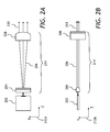
- Figs. 2A, 2B are schematic views of a two-lens anamorphic telescope for collimating radiation from an individual laser diode emitter;
- Figs. 3A, 3B depict a layout of a basic two-emitter optical unit according to the present invention
- Fig. 4A is a plan view of the light source according to the present invention.
- Fig. 4B is a front view of the light source according to the present invention.
- Figs. 5A, 5B represent optical design software rendering of the optical beam paths in the light source according to the present invention
- Fig. 6 is a 3D view of package of seven laser diode emitters.
- FIG. 1 a layout is shown of a prior art apparatus 100 for coupling radiation beams into an optical fiber.
- the apparatus 100 is comprised of individual laser diode emitter chips 111a - 111f, each having coupled thereto a set of collimating micro-optics 131a - 131f, a multi-faceted redirecting mirror, or unitary deflector 120, focusing optics 151, and an output optical fiber 170 having a cladding 171.
- the emitting apertures of the emitter chips 111a - 111f are imaged by an afocal relay optical system onto a unitary deflector 120 which redirects the radiation towards a common output afocal relay system 151 which couples the radiation from emitters 111a - 111f into cladding 171 of output fiber 170.
- Figs. 2A and 2B illustrate a basic optical configuration, in plan and side views, respectively, for collimating radiation from individual laser diode emitters, employed in the apparatus of present invention.
- a planar semiconductor laser diode 202 disposed in an XZ plane 212A emits an optical beam 206 that is collimated in an YZ plane 212B by a fast-axis collimating lens 204.
- the lens 204 can be cylindrical, or, more generally, toroidal in shape, such that while the divergence of beam 206 in YZ plane 212B is minimized, the divergence of beam 206 in XZ plane 212A is nearly unaffected.
- the beam 206 propagates towards a slow-axis collimating lens 208, which can also be cylindrical or toroidal.
- the function of lens 208 is to collimate the beam 206 in XZ plane 212A, such that an output beam 210 is collimated in both planes; XZ plane 212A and YZ plane 212B.
- FIG. 3A is a plan view, and a front view is shown in Fig. 3B .
- Two planar semiconductor laser diodes 302 and 303 disposed parallel to an XZ plane 312A but offset along an Y-axis 312B as is seen in Fig. 3B , emit optical beams 306 and 307 collimated along Y-axis 312B by fast-axis collimating lenses 304 and 305, respectively.
- the beams 306 and 307 are deflected by mirrors 316 and 317, which are arranged on the top of one another, so as to direct the beams 306 and 307 towards a slow-axis collimating lens 308.
- the spot profiles of anamorphic beams 306 and 307 on mirrors 316 and 317 are shown with ellipses 318 and 319, respectively, in Fig. 3B .
- the beams 310 After being collimated by the slow-axis collimating lens 308, the beams 310 are located one under another when viewed in the XZ plane 312A of Fig. 3A .
- Figs. 3A and 3B are similar to that of Figs. 2A and 2B in a sense that both arrangements use an anamorphic telescope such as telescope 214, to reformat and collimate radiation of a laser diode, with the difference being that a folding mirror is used between the two lenses of a telescope in Figs. 3A and 3B .
- the advantage of arrangement of Figs. 3A and 3B besides sharing the common optical element 308, is that it effectively utilizes the area on both sides of optical axis 320 of the slow-axis collimating lens 308 while effectively heat-sinking laser diodes 302 and 303.
- output beams 310 from laser diodes 302 and 303 can be aligned independently: first, the fast-axis collimating lens 304 and folding mirror 316 for laser diode 302 are aligned and fixed, and then the optics 305 and 317 for laser diode 303 are aligned, and fixed.
- Yet another advantage of the arrangement shown in Figs. 3A and 3B is that it can be used as a building block for adding more and more laser diode pairs into the same optical package, as is described below.
- a schematic layout of a diode laser 400 consisting of seven individual planar laser diode emitters, is shown. Of these seven emitters, two emitters 402 and 403, disposed parallel to an XZ plane 412A, emit optical beams 406 and 407 collimated in a fast-axis plane by fast-axis collimating lenses 404 and 405, respectively.
- the beams 406 and 407 are deflected by mirrors 416 and 417, which are arranged on top of one another, so as to direct both beams 406 and 407 towards a slow-axis collimating lens 408.
- the beams 410 After being collimated by the slow-axis collimated lens 408, the beams 410 are located one under another when viewed in the XZ plane 412A of Fig. 4A . As one can see, the arrangement so far is very similar to that of Fig. 3A . However, in Fig. 4A , two more pairs of laser diodes, associated with respective fast-axis collimating optics and folding mirrors, are present in the layout of the laser 400. The location of these two additional pairs of diodes is marked with dotted boxes 420 and 422. Boxes 420 and 422 encompass the same set of elements as the group of elements 402, 404, 406, 416, 417, 407, 405, and 403.
- Fig. 4A one more laser diode chip 426, coupled to a fast-axis collimating lens 424, is shown at the top of Fig. 4A .
- the lenses 424 and 408 form an anamorphic telescope similar to the telescope 214 of Figs. 2A and 2B .
- the laser diode chips in boxes 420 and 422 are located closer to respective folding mirrors than lasers 402 and 403 since the distances between a laser diode chip emitting end and the common slow-axis collimating lens 408 are chosen to be equal. In this way, the slow-axis collimating condition will be fulfilled for all the laser diodes simultaneously.
- a focusing lens 428 can now focus the radiation from all laser diodes into an optical fiber 430.
- Fig. 4B a schematic view of the diode laser 400 is shown in a front-view XY plane 412B.
- Two planar semiconductor laser diodes 402 and 403 emit optical beams 406 and 407 collimated along a Y-axis of the coordinate system 412B by fast-axis collimating lenses 404 and 405, respectively.
- the beams 406 and 407 are deflected by mirrors 416 and 417, which are arranged on top of one another, so as to direct both beams 406 and 407 towards the slow-axis collimated lens 408 shown in a plan view.
- the spot profiles of anamorphic beams 406 and 407 on mirrors 416 and 417 are shown with ellipses 418 and 419, respectively.
- the two other pairs of laser diodes associated each with a fast axis collimating lens and a folding mirror, are shown schematically inside boxes 420 and 422. In the view of Fig. 4B , these pairs of laser diodes are disposed one on a top of the other.
- the laser diode chip 426 of Fig. 4A emits light collimated in Y-direction by a fast-axis collimating lens 424.
- An ellipse 432 represents a lateral beam profile of the beam collimated in fast axis direction by the lens 424.
- ellipses 434-440 represent lateral beam profiles of the fast-axis collimated optical beams from the other laser diode chips of the diode laser 400.
- the focal lengths of the lenses and the distances between the lenses and between a fast-axis collimating lens and a laser diode chip By choosing the focal lengths of the lenses and the distances between the lenses and between a fast-axis collimating lens and a laser diode chip, one can design the ellipses 418, 419, and 432-440 to fill the aperture of the slow-axis collimating lens 408.
- the ellipse axis ratio should be approximately equal to 1/n, where n is the amount of laser diode chips in the diode laser assembly 400.
- the arrangement allows for very compact packaging of laser diode chips and associated optics into a rhombic package 442 of Fig. 4A . Since the laser chips of the diode laser 400 are disposed close to a perimeter of the rhomb 442, their thermal coupling to each other is minimal, and effective heat sinking to a common heat sink is optimized as a result. Moreover, the laser diode chips are conveniently located for serial connection, to reduce the maximum current supplied to the diode laser 400.
- Figs. 5A and 5B are optical design software renderings of the beam paths in an XZ plane 512A and an YZ plane 512B, respectively.
- Light from four emitters (not shown) is collimated in YZ plane 512B by cylindrical lenses 504A-504D seen as one lens 504 on Fig. 5A .
- Optical beams 506A-506D propagate towards a slow-axis collimating lens 508.
- the beams 506A-506D are seen as one beam 506 in Fig. 5A because the beams are propagating one under another being shifted along the Y-axis.
- the slow-axis collimating lens 508 collimates the four beams 506A-506D, so that they propagate as a compound beam 510 towards a focusing lens 528 which focuses individual beams 542A-542D into a single spot 544.
- the folding mirrors are not shown in Figs 5A and 5B for simplicity.
- Fig. 6 shows a 3D view of a prototype 600 of the fiber-coupled diode laser light source of present invention. It consists of a hermetically sealable package 602, which serves at the same time as a compound heat sink for seven laser diode single emitter chips 611-617. The single emitter chips are connected electrically in series, the driving current being supplied through terminals 604 and 606.
- a ferrule 608 holds an output optical fiber 610. Disposed in front of the fiber 610 are the focusing lens 620 and a slow-axis collimating cylindrical lens 618. Three pairs of folding mirrors are also seen in Fig.
- the fiber 6 is a multimode fiber with a diameter of 105 microns and a numerical aperture of 0.22.
Landscapes
- Physics & Mathematics (AREA)
- General Physics & Mathematics (AREA)
- Optics & Photonics (AREA)
- Condensed Matter Physics & Semiconductors (AREA)
- Electromagnetism (AREA)
- Semiconductor Lasers (AREA)
- Optical Couplings Of Light Guides (AREA)
Applications Claiming Priority (1)
| Application Number | Priority Date | Filing Date | Title |
|---|---|---|---|
| US93432007P | 2007-06-12 | 2007-06-12 |
Publications (2)
| Publication Number | Publication Date |
|---|---|
| EP2003484A1 true EP2003484A1 (de) | 2008-12-17 |
| EP2003484B1 EP2003484B1 (de) | 2018-04-11 |
Family
ID=39714136
Family Applications (1)
| Application Number | Title | Priority Date | Filing Date |
|---|---|---|---|
| EP08155305.9A Active EP2003484B1 (de) | 2007-06-12 | 2008-04-28 | Lichtquelle |
Country Status (4)
| Country | Link |
|---|---|
| US (1) | US7668214B2 (de) |
| EP (1) | EP2003484B1 (de) |
| JP (1) | JP5268437B2 (de) |
| CN (1) | CN101324321B (de) |
Cited By (8)
| Publication number | Priority date | Publication date | Assignee | Title |
|---|---|---|---|---|
| WO2010138190A1 (en) * | 2009-05-28 | 2010-12-02 | Eastman Kodak Company | Beam alignment system using arrayed light sources |
| US7959297B2 (en) | 2008-05-15 | 2011-06-14 | Eastman Kodak Company | Uniform speckle reduced laser projection using spatial and temporal mixing |
| US8066389B2 (en) | 2009-04-30 | 2011-11-29 | Eastman Kodak Company | Beam alignment chamber providing divergence correction |
| US8132919B2 (en) | 2009-04-30 | 2012-03-13 | Eastman Kodak Company | Digital projector using arrayed light sources |
| WO2012032116A1 (de) | 2010-09-09 | 2012-03-15 | Limo Patentverwaltung Gmbh & Co. Kg | Laservorrichtung zur erzeugung einer linienförmigen intensitätsverteilung in einer arbeitsebene |
| CN105759411A (zh) * | 2016-04-15 | 2016-07-13 | 武汉凌云光电科技有限责任公司 | 光纤耦合激光器、光纤耦合激光器系统及其优化方法 |
| CN109960042A (zh) * | 2019-04-26 | 2019-07-02 | 杭州晟创激光科技有限公司 | 一种多线束激光照明光源 |
| WO2023118950A1 (en) * | 2021-12-22 | 2023-06-29 | Bosch Car Multimedia Portugal, S.A. | Multiwavelength optical road condition sensor with single emission point |
Families Citing this family (33)
| Publication number | Priority date | Publication date | Assignee | Title |
|---|---|---|---|---|
| US7733932B2 (en) * | 2008-03-28 | 2010-06-08 | Victor Faybishenko | Laser diode assemblies |
| US7773655B2 (en) * | 2008-06-26 | 2010-08-10 | Vadim Chuyanov | High brightness laser diode module |
| US8427749B2 (en) | 2010-06-30 | 2013-04-23 | Jds Uniphase Corporation | Beam combining light source |
| US8437086B2 (en) | 2010-06-30 | 2013-05-07 | Jds Uniphase Corporation | Beam combining light source |
| DE102010031199B4 (de) | 2010-07-09 | 2020-05-14 | Jenoptik Optical Systems Gmbh | Vorrichtung und Verfahren zur Strahlformung |
| US8432945B2 (en) | 2010-09-30 | 2013-04-30 | Victor Faybishenko | Laser diode combiner modules |
| GB2495774A (en) * | 2011-10-21 | 2013-04-24 | Barco Nv | Laser diode grid element comprised of standard laser diodes on a heat exchange plate and PCB |
| US8861082B2 (en) * | 2012-02-21 | 2014-10-14 | Corning Incorporated | Method and apparatus for combining laser array light sources |
| CN102809823B (zh) * | 2012-08-23 | 2015-05-06 | 中国兵器工业第二0五研究所 | 激光合束照射与接收系统 |
| JP5920254B2 (ja) * | 2013-03-13 | 2016-05-18 | ウシオ電機株式会社 | 半導体レーザ装置 |
| KR101455800B1 (ko) * | 2013-09-06 | 2014-11-03 | (주)코셋 | 레이저 다이오드 모듈 및 이에 이용되는 광학구조물 |
| JP6351090B2 (ja) * | 2013-09-13 | 2018-07-04 | Zero Lab株式会社 | 光源ユニット、光源ユニットを用いた照明光学系 |
| CN103579905B (zh) * | 2013-11-11 | 2016-02-10 | 西北大学 | 空间叠加耦合高功率半导体激光叠阵系统 |
| DE102013112502B4 (de) * | 2013-11-13 | 2022-05-05 | Focuslight (Hai Ning) Optoelectronics Co., LTD | Verfahren und Anordnung zur Symmetrisierung eines Poynting-Fehlers eines aus mindestens zwei Strahlenbündeln durch Strahlumlenkung zusammengesetzten Laserstrahls |
| US9647416B2 (en) | 2013-12-23 | 2017-05-09 | Lumentum Operations Llc | Bidirectional long cavity semiconductor laser for improved power and efficiency |
| JP2015153889A (ja) * | 2014-02-14 | 2015-08-24 | 三菱電機株式会社 | レーザ合成光学装置 |
| CA3238721A1 (en) * | 2014-08-14 | 2016-02-18 | Mtt Innovation Incorporated | Multiple-laser light source |
| US20160119063A1 (en) | 2014-10-24 | 2016-04-28 | Lumentum Operations Llc | Wavelength locking and multiplexing of high-power semiconductor lasers |
| CN104836113A (zh) * | 2015-05-18 | 2015-08-12 | 浙江合波光学科技有限公司 | 一种多单管大功率光纤耦合半导体激光器 |
| CN105071196B (zh) * | 2015-07-21 | 2019-01-15 | 北京杏林睿光科技有限公司 | 一种窄线宽合束模块及具有该模块的多波长拉曼激光器 |
| JP2019015769A (ja) * | 2017-07-04 | 2019-01-31 | 株式会社島津製作所 | 光結合モジュール |
| JP7080971B2 (ja) | 2017-11-01 | 2022-06-06 | ヌブル インク | マルチkWクラスの青色レーザーシステム |
| WO2019130060A2 (en) | 2017-12-29 | 2019-07-04 | Casela Technologies | Fiber optic photon engine |
| JP6636062B2 (ja) * | 2018-01-11 | 2020-01-29 | 三菱電機株式会社 | レーザ合成光学装置 |
| WO2019187784A1 (ja) * | 2018-03-26 | 2019-10-03 | パナソニック株式会社 | 光学装置 |
| CN108429129A (zh) * | 2018-05-08 | 2018-08-21 | 中国科学院半导体研究所 | 多线阵半导体激光器光栅外腔光谱的合束系统及方法 |
| RU2688888C1 (ru) * | 2018-05-14 | 2019-05-22 | Российская Федерация, от имени которой выступает Государственная корпорация по атомной энергии "Росатом" (Госкорпорация "Росатом") | Лазерный модуль и способ его изготовления |
| CN108808436B (zh) * | 2018-06-20 | 2020-01-14 | 中国工程物理研究院应用电子学研究所 | 一种基于平板合束器的多光束共孔径相干合成装置 |
| JP7372308B2 (ja) * | 2019-02-27 | 2023-10-31 | ヌヴォトンテクノロジージャパン株式会社 | 半導体レーザモジュール |
| DE102020118421B4 (de) * | 2020-07-13 | 2023-08-03 | Focuslight Technologies Inc. | Laservorrichtung |
| CN114545565A (zh) * | 2020-11-24 | 2022-05-27 | 华为技术有限公司 | 一种光器件 |
| CN113381270A (zh) * | 2021-04-21 | 2021-09-10 | 深圳市瑞沃德生命科技有限公司 | 一种激光器及具有其的激光理疗装置 |
| CA3126975A1 (en) | 2021-08-05 | 2023-02-05 | Com Dev Ltd. | Quantum key distribution system |
Citations (4)
| Publication number | Priority date | Publication date | Assignee | Title |
|---|---|---|---|---|
| WO2002050599A1 (en) * | 2000-12-18 | 2002-06-27 | Rayteq Photonic Solutions Ltd. | Optical device for unifying light beams emitted by several light sources |
| US20030099267A1 (en) * | 2000-12-06 | 2003-05-29 | Petra Hennig | Diode laser arrangement with several diode laser rows |
| EP1619765A1 (de) * | 2004-07-19 | 2006-01-25 | TRUMPF Laser GmbH + Co.KG | Diodenlaseranordnung und Strahlformungseinheit dafür |
| WO2007019878A1 (de) * | 2005-08-19 | 2007-02-22 | Limo Patentverwaltung Gmbh & Co. Kg | Laseranordnung |
Family Cites Families (20)
| Publication number | Priority date | Publication date | Assignee | Title |
|---|---|---|---|---|
| GB1040792A (en) * | 1964-02-24 | 1966-09-01 | Nat Res Dev | Optical systems for lasers |
| JPS63272092A (ja) * | 1987-04-30 | 1988-11-09 | Yoshiaki Arata | 超強力複合レ−ザ・ビ−ム造出法 |
| US5048911A (en) * | 1988-11-15 | 1991-09-17 | Universiti Malaya | Coupling of multiple laser beams to a single optical fiber |
| US5185758A (en) * | 1989-11-28 | 1993-02-09 | Massachusetts Institute Of Technology | Multiple-laser pump optical system |
| US5081637A (en) * | 1989-11-28 | 1992-01-14 | Massachusetts Institute Of Technology | Multiple-laser pump optical system |
| DE69132049T3 (de) | 1990-08-01 | 2004-09-02 | Diomed Ltd. | Hochleistungs-lichtquelle |
| US5268978A (en) * | 1992-12-18 | 1993-12-07 | Polaroid Corporation | Optical fiber laser and geometric coupler |
| US5418880A (en) * | 1994-07-29 | 1995-05-23 | Polaroid Corporation | High-power optical fiber amplifier or laser device |
| US6124973A (en) * | 1996-02-23 | 2000-09-26 | Fraunhofer Gesellschaft Zur Foerderung Der Angewandten Forschung E.V. | Device for providing the cross-section of the radiation emitted by several solid-state and/or semiconductor diode lasers with a specific geometry |
| US6044096A (en) * | 1997-11-03 | 2000-03-28 | Sdl, Inc. | Packaged laser diode array system and method with reduced asymmetry |
| US6229831B1 (en) * | 1997-12-08 | 2001-05-08 | Coherent, Inc. | Bright diode-laser light-source |
| US6151342A (en) * | 1997-12-08 | 2000-11-21 | Coherent, Inc. | Bright diode-laser light-source |
| DE19800590B4 (de) * | 1998-01-09 | 2005-12-01 | Jenoptik Ag | Optische Anordnung zur Symmetrierung der Strahlung eines oder mehrerer übereinander angeordneter Hochleistungsdiodenlaser |
| US6324320B1 (en) * | 1998-03-17 | 2001-11-27 | Polaroid Corporation | Optical apparatus for producing a high-brightness multi-laser radiation source |
| US6075912A (en) * | 1998-03-17 | 2000-06-13 | Polaroid Corporation | Apparatus for coupling radiation beams into an optical waveguide |
| US6005717A (en) * | 1998-11-17 | 1999-12-21 | Ceramoptec Industries, Inc. | Diode laser beam combiner system |
| GB0312443D0 (en) * | 2003-05-30 | 2003-07-09 | Newoptics Ltd | Optical multiplexer |
| JP2008501144A (ja) * | 2004-06-01 | 2008-01-17 | トルンプ フォトニクス,インコーポレイテッド | 光ファイバへの2次元のレーザアレイスタックの出力の最適な整合 |
| JP2006309146A (ja) * | 2005-03-31 | 2006-11-09 | Fuji Photo Film Co Ltd | 光源モジュール |
| US20070116077A1 (en) * | 2005-11-22 | 2007-05-24 | Nlight Photonics Corporation | Vertically displaced stack of multi-mode single emitter laser diodes |
-
2008
- 2008-04-28 EP EP08155305.9A patent/EP2003484B1/de active Active
- 2008-05-07 US US12/116,834 patent/US7668214B2/en active Active
- 2008-06-11 JP JP2008153242A patent/JP5268437B2/ja active Active
- 2008-06-11 CN CN2008101111720A patent/CN101324321B/zh active Active
Patent Citations (5)
| Publication number | Priority date | Publication date | Assignee | Title |
|---|---|---|---|---|
| US20030099267A1 (en) * | 2000-12-06 | 2003-05-29 | Petra Hennig | Diode laser arrangement with several diode laser rows |
| WO2002050599A1 (en) * | 2000-12-18 | 2002-06-27 | Rayteq Photonic Solutions Ltd. | Optical device for unifying light beams emitted by several light sources |
| EP1619765A1 (de) * | 2004-07-19 | 2006-01-25 | TRUMPF Laser GmbH + Co.KG | Diodenlaseranordnung und Strahlformungseinheit dafür |
| US20060018356A1 (en) * | 2004-07-19 | 2006-01-26 | Andreas Voss | Diode laser arrangement and associated beam shaping unit |
| WO2007019878A1 (de) * | 2005-08-19 | 2007-02-22 | Limo Patentverwaltung Gmbh & Co. Kg | Laseranordnung |
Cited By (12)
| Publication number | Priority date | Publication date | Assignee | Title |
|---|---|---|---|---|
| US7959297B2 (en) | 2008-05-15 | 2011-06-14 | Eastman Kodak Company | Uniform speckle reduced laser projection using spatial and temporal mixing |
| US8066389B2 (en) | 2009-04-30 | 2011-11-29 | Eastman Kodak Company | Beam alignment chamber providing divergence correction |
| US8132919B2 (en) | 2009-04-30 | 2012-03-13 | Eastman Kodak Company | Digital projector using arrayed light sources |
| WO2010138190A1 (en) * | 2009-05-28 | 2010-12-02 | Eastman Kodak Company | Beam alignment system using arrayed light sources |
| US8033666B2 (en) | 2009-05-28 | 2011-10-11 | Eastman Kodak Company | Beam alignment system using arrayed light sources |
| CN102449532A (zh) * | 2009-05-28 | 2012-05-09 | 伊斯曼柯达公司 | 使用阵列光源的光束对准系统 |
| WO2012032116A1 (de) | 2010-09-09 | 2012-03-15 | Limo Patentverwaltung Gmbh & Co. Kg | Laservorrichtung zur erzeugung einer linienförmigen intensitätsverteilung in einer arbeitsebene |
| US8967826B2 (en) | 2010-09-09 | 2015-03-03 | Limo Patentverwaltung Gmbh & Co. Kg | Laser apparatus for generating a line-shaped intensity distribution in a working plane |
| CN105759411A (zh) * | 2016-04-15 | 2016-07-13 | 武汉凌云光电科技有限责任公司 | 光纤耦合激光器、光纤耦合激光器系统及其优化方法 |
| CN105759411B (zh) * | 2016-04-15 | 2019-02-19 | 武汉凌云光电科技有限责任公司 | 光纤耦合激光器、光纤耦合激光器系统及其优化方法 |
| CN109960042A (zh) * | 2019-04-26 | 2019-07-02 | 杭州晟创激光科技有限公司 | 一种多线束激光照明光源 |
| WO2023118950A1 (en) * | 2021-12-22 | 2023-06-29 | Bosch Car Multimedia Portugal, S.A. | Multiwavelength optical road condition sensor with single emission point |
Also Published As
| Publication number | Publication date |
|---|---|
| US20080310027A1 (en) | 2008-12-18 |
| CN101324321A (zh) | 2008-12-17 |
| JP2008311655A (ja) | 2008-12-25 |
| US7668214B2 (en) | 2010-02-23 |
| JP5268437B2 (ja) | 2013-08-21 |
| CN101324321B (zh) | 2013-05-22 |
| EP2003484B1 (de) | 2018-04-11 |
Similar Documents
| Publication | Publication Date | Title |
|---|---|---|
| EP2003484B1 (de) | Lichtquelle | |
| US9065237B2 (en) | High-brightness spatial-multiplexed multi-emitter pump with tilted collimated beam | |
| US6700709B1 (en) | Configuration of and method for optical beam shaping of diode laser bars | |
| EP2403078B1 (de) | Strahlenkombinierende Lichtquelle | |
| US8437086B2 (en) | Beam combining light source | |
| US7515346B2 (en) | High power and high brightness diode-laser array for material processing applications | |
| US6778732B1 (en) | Generation of high-power, high brightness optical beams by optical cutting and beam-shaping of diode lasers | |
| US9455552B1 (en) | Laser diode apparatus utilizing out of plane combination | |
| CN101833150B (zh) | 一种大功率半导体激光器光纤耦合模块 | |
| US20190252863A1 (en) | Diode laser apparatus with fac lens out-of-plane beam steering | |
| US7773653B2 (en) | Diode laser arrangement and associated beam shaping unit | |
| CN110299668B (zh) | 多个二极管激光模块的构造及其操作方法 | |
| US7110183B2 (en) | Device for the optical beam transformation of a linear arrangement of several light sources | |
| US20090245315A1 (en) | Laser diode assemblies | |
| KR101729341B1 (ko) | 레이저 빔 인터리빙 | |
| JP2015501508A (ja) | 光源システムおよびレーザ光源 | |
| EP2342597B1 (de) | Verschachtelung von laserstrahlen | |
| US20040146083A1 (en) | Apparatus for shaping the output beam of semiconductor lasers | |
| CN112310800A (zh) | 一种紧凑式光纤耦合输出半导体激光器 | |
| CN115427859A (zh) | 激光装置 | |
| CN223431071U (zh) | 光源组件 | |
| CN222839236U (zh) | 一种双波长半导体激光模组及激光器 | |
| KR102529166B1 (ko) | 레이저 모듈 패키지 | |
| US20230411934A1 (en) | Slow axis, or slow axis and fast axis, wavelength beam combining for laser minibars | |
| KR20250064870A (ko) | 레이저 다이오드 패키지 |
Legal Events
| Date | Code | Title | Description |
|---|---|---|---|
| PUAI | Public reference made under article 153(3) epc to a published international application that has entered the european phase |
Free format text: ORIGINAL CODE: 0009012 |
|
| AK | Designated contracting states |
Kind code of ref document: A1 Designated state(s): AT BE BG CH CY CZ DE DK EE ES FI FR GB GR HR HU IE IS IT LI LT LU LV MC MT NL NO PL PT RO SE SI SK TR |
|
| AX | Request for extension of the european patent |
Extension state: AL BA MK RS |
|
| 17P | Request for examination filed |
Effective date: 20090616 |
|
| 17Q | First examination report despatched |
Effective date: 20090715 |
|
| AKX | Designation fees paid |
Designated state(s): DE FR GB |
|
| RAP1 | Party data changed (applicant data changed or rights of an application transferred) |
Owner name: LUMENTUM OPERATIONS LLC |
|
| GRAP | Despatch of communication of intention to grant a patent |
Free format text: ORIGINAL CODE: EPIDOSNIGR1 |
|
| INTG | Intention to grant announced |
Effective date: 20160909 |
|
| GRAJ | Information related to disapproval of communication of intention to grant by the applicant or resumption of examination proceedings by the epo deleted |
Free format text: ORIGINAL CODE: EPIDOSDIGR1 |
|
| STAA | Information on the status of an ep patent application or granted ep patent |
Free format text: STATUS: EXAMINATION IS IN PROGRESS |
|
| INTC | Intention to grant announced (deleted) | ||
| GRAP | Despatch of communication of intention to grant a patent |
Free format text: ORIGINAL CODE: EPIDOSNIGR1 |
|
| STAA | Information on the status of an ep patent application or granted ep patent |
Free format text: STATUS: GRANT OF PATENT IS INTENDED |
|
| INTG | Intention to grant announced |
Effective date: 20171107 |
|
| GRAS | Grant fee paid |
Free format text: ORIGINAL CODE: EPIDOSNIGR3 |
|
| GRAA | (expected) grant |
Free format text: ORIGINAL CODE: 0009210 |
|
| STAA | Information on the status of an ep patent application or granted ep patent |
Free format text: STATUS: THE PATENT HAS BEEN GRANTED |
|
| AK | Designated contracting states |
Kind code of ref document: B1 Designated state(s): DE FR GB |
|
| REG | Reference to a national code |
Ref country code: GB Ref legal event code: FG4D |
|
| REG | Reference to a national code |
Ref country code: FR Ref legal event code: PLFP Year of fee payment: 11 |
|
| REG | Reference to a national code |
Ref country code: DE Ref legal event code: R096 Ref document number: 602008054755 Country of ref document: DE |
|
| REG | Reference to a national code |
Ref country code: DE Ref legal event code: R097 Ref document number: 602008054755 Country of ref document: DE |
|
| PLBE | No opposition filed within time limit |
Free format text: ORIGINAL CODE: 0009261 |
|
| STAA | Information on the status of an ep patent application or granted ep patent |
Free format text: STATUS: NO OPPOSITION FILED WITHIN TIME LIMIT |
|
| 26N | No opposition filed |
Effective date: 20190114 |
|
| PGFP | Annual fee paid to national office [announced via postgrant information from national office to epo] |
Ref country code: DE Payment date: 20250430 Year of fee payment: 18 |
|
| PGFP | Annual fee paid to national office [announced via postgrant information from national office to epo] |
Ref country code: FR Payment date: 20250430 Year of fee payment: 18 |
|
| PGFP | Annual fee paid to national office [announced via postgrant information from national office to epo] |
Ref country code: GB Payment date: 20260331 Year of fee payment: 19 |