EP2000828B1 - Système de focalisation comprenant un modulateur de lumière - Google Patents
Système de focalisation comprenant un modulateur de lumière Download PDFInfo
- Publication number
- EP2000828B1 EP2000828B1 EP08016546.7A EP08016546A EP2000828B1 EP 2000828 B1 EP2000828 B1 EP 2000828B1 EP 08016546 A EP08016546 A EP 08016546A EP 2000828 B1 EP2000828 B1 EP 2000828B1
- Authority
- EP
- European Patent Office
- Prior art keywords
- layers
- deformable
- electrode
- cells
- signal electrodes
- Prior art date
- Legal status (The legal status is an assumption and is not a legal conclusion. Google has not performed a legal analysis and makes no representation as to the accuracy of the status listed.)
- Expired - Lifetime
Links
- 230000003287 optical effect Effects 0.000 abstract description 11
- 239000000499 gel Substances 0.000 description 28
- 239000004205 dimethyl polysiloxane Substances 0.000 description 7
- 229920000435 poly(dimethylsiloxane) Polymers 0.000 description 7
- -1 polydimethylsiloxane Polymers 0.000 description 7
- 239000000758 substrate Substances 0.000 description 7
- BOTDANWDWHJENH-UHFFFAOYSA-N Tetraethyl orthosilicate Chemical compound CCO[Si](OCC)(OCC)OCC BOTDANWDWHJENH-UHFFFAOYSA-N 0.000 description 5
- ATJFFYVFTNAWJD-UHFFFAOYSA-N Tin Chemical compound [Sn] ATJFFYVFTNAWJD-UHFFFAOYSA-N 0.000 description 5
- 239000003054 catalyst Substances 0.000 description 3
- 239000003431 cross linking reagent Substances 0.000 description 3
- 238000000034 method Methods 0.000 description 3
- 239000000203 mixture Substances 0.000 description 3
- LCGLNKUTAGEVQW-UHFFFAOYSA-N Dimethyl ether Chemical compound COC LCGLNKUTAGEVQW-UHFFFAOYSA-N 0.000 description 2
- 229910007161 Si(CH3)3 Inorganic materials 0.000 description 2
- 230000001419 dependent effect Effects 0.000 description 2
- 229920001296 polysiloxane Polymers 0.000 description 2
- 230000015572 biosynthetic process Effects 0.000 description 1
- 239000003989 dielectric material Substances 0.000 description 1
- KPUWHANPEXNPJT-UHFFFAOYSA-N disiloxane Chemical class [SiH3]O[SiH3] KPUWHANPEXNPJT-UHFFFAOYSA-N 0.000 description 1
- 239000000428 dust Substances 0.000 description 1
- 230000005684 electric field Effects 0.000 description 1
- 230000001788 irregular Effects 0.000 description 1
- 230000003647 oxidation Effects 0.000 description 1
- 238000007254 oxidation reaction Methods 0.000 description 1
- 239000000126 substance Substances 0.000 description 1
Images

Classifications
-
- G—PHYSICS
- G02—OPTICS
- G02B—OPTICAL ELEMENTS, SYSTEMS OR APPARATUS
- G02B26/00—Optical devices or arrangements for the control of light using movable or deformable optical elements
- G02B26/08—Optical devices or arrangements for the control of light using movable or deformable optical elements for controlling the direction of light
- G02B26/0808—Optical devices or arrangements for the control of light using movable or deformable optical elements for controlling the direction of light by means of one or more diffracting elements
-
- G—PHYSICS
- G02—OPTICS
- G02B—OPTICAL ELEMENTS, SYSTEMS OR APPARATUS
- G02B27/00—Optical systems or apparatus not provided for by any of the groups G02B1/00 - G02B26/00, G02B30/00
- G02B27/50—Optics for phase object visualisation
- G02B27/54—Schlieren-optical systems
-
- H—ELECTRICITY
- H04—ELECTRIC COMMUNICATION TECHNIQUE
- H04N—PICTORIAL COMMUNICATION, e.g. TELEVISION
- H04N9/00—Details of colour television systems
- H04N9/12—Picture reproducers
- H04N9/31—Projection devices for colour picture display, e.g. using electronic spatial light modulators [ESLM]
- H04N9/3102—Projection devices for colour picture display, e.g. using electronic spatial light modulators [ESLM] using two-dimensional electronic spatial light modulators
-
- H—ELECTRICITY
- H04—ELECTRIC COMMUNICATION TECHNIQUE
- H04N—PICTORIAL COMMUNICATION, e.g. TELEVISION
- H04N9/00—Details of colour television systems
- H04N9/12—Picture reproducers
- H04N9/31—Projection devices for colour picture display, e.g. using electronic spatial light modulators [ESLM]
- H04N9/3141—Constructional details thereof
Definitions
- This invention relates to light modulators used in optical systems.
- the invention is more particularly concerned with optical systems using light modulators which rely upon the creation of a surface relief under the action of an electric field.
- modulators have been known for many years, and for example in 1939 F. Fischer disclosed an "electro-optical transformer" using an oil layer and Schlieren optics. More recently, consideration has been given to modulators which rely upon the creation of a relief on a gel of a suitable non-polar dielectric material, such as a siloxane gel. A comprehensive discussion of such systems can be found in the book " Physics of Reliefography” by Professor Yuri Guscho published in Moscow in 1999, ISBN 5-8213-0039-8 .
- a light modulator which has been found to be successful comprises two deformable dielectric layers of different refractive coefficients, at least one of which is a gel. Typically the other layer may be air. Electrodes are provided either side of the layers, and reliefs are generated at the interface between the two layers in response to applied signals.
- Polyorganosiloxane gels are particularly preferred for use as the gel layer in such modulators.
- One suitable gel is prepared by adding tetraethoxysilane, as a cross linking agent, and tin diethyldicaprylate, as a catalyst, to a solution of a ⁇ , ⁇ -dihydroxypolydimethylsiloxane of general formula : HO-Si(CH 3 ) 2 O[-SiO(CH 3 ) 2 -] n Si(CH 3 ) 2 -OH in a polydimethylsiloxane of general formula : (CH 3 ) 3 SiO[-SiO(CH 3 ) 2 -] n Si(CH 3 ) 3
- Such a gel has several advantages. It is transparent, flexible, and has good optical properties. It exhibits good response times in the formation of reliefs. It is stable and can withstand high temperatures.
- the present invention concerns the use of a light modulator in a novel way. Instead of being used to produce images in accordance with applied signal, the modulator is used as a more passive element in an optical system.
- a focusing system as defined.
- the relief surface of the deformable gel layer can be changed to alter the focal length of the lens.
- the focal length can be varied, the rate being dependent on the rate of development of a relief.
- a lens whose properties can be changed rapidly.
- Such a lens may be used in many optical systems, such a laboratory equipment, cameras, projectors, or even spectacles.
- Preferably different voltages are applied to the signal electrodes of all cells of the light modulator so that the distribution of the electric potential across the plane of the signal electrodes and at the interface between the deformable layers is not rastered, which enables space-time control of the relief shape in accordance with desired laws.
- the radial extent of the signal electrodes reduces from the innermost ring to the outermost ring.
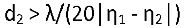
- the following criteria are met for each cell): 0.01 d 1 ⁇ d 2 ⁇ d 1 d 2 > ⁇ / 20 ⁇ 1 ⁇ ⁇ 2 ⁇ 1 ⁇ ⁇ 2 > 0.1 t ⁇ > 0.01 ⁇ m 0.1 d 1 ⁇ L ⁇ 10 d 1 in which d 2 is the distance between the signal electrode and the interface between the deformable layers; d 1 is the distance between the first electrode and the interface between the deformable layers; ⁇ is the wavelength of light with which the cell is used; ⁇ 1 is the refractive coefficient of one of the deformable layers; ⁇ 2 is the refractive coefficient of the other of the deformable layers; t ⁇ is the duration of voltage pulses applied to the signal electrodes; ⁇ m is the time constant of mechanical relaxation of the relief formed at the interface between the layers; and L is the minimum spatial period between electrodes in adjacent cells.
- the relief forming gel is a polyorganosiloxane gel.
- the preferred cross-linkable polysiloxane is ⁇ , ⁇ -dihydroxypolydimethylsiloxane of general formula : HO-Si(CH 3 ) 2 O[-SiO(CH 3 ) 2 -] n Si(CH 3 ) 2 -OH
- the preferred polysiloxane is a polydimethylsiloxane of general formula : (CH 3 ) 3 SiO[-SiO(CH 3 ) 2 -] n Si(CH 3 ) 3
- the preferred cross linking agent is tetraethoxysilane
- the preferred catalyst is tin diethyldicaprylate.
- the ⁇ , ⁇ -dihydroxypolydimethylsiloxane is in the polydimethylsiloxane as a 10 - 30% solution, and for example a 15% solution.
- the methods use ⁇ , ⁇ -dihydroxypolydimethylsiloxane having a molar mass of (1-2)10 4 g/mol in polydimethylsiloxane having a molar mass of (0.6-1) ⁇ 10 3 g/mol, at the 1:0.8-1:1.5 and 1:2-1:5 ⁇ , ⁇ -dihydroxy-polydimethylsiloxane / tin diethyldicaprylate and ⁇ , ⁇ -dihydroxypolydimethylsiloxane / tetraethoxysilane molar ratios.
- a layer of a substance which will increase adhesion of the gel to the substrate such as a polycarboarylenesiloxane film.
- the components will be mixed together in appropriate quantities.
- tetraethoxysilane and tin diethyldicaprylate will be added to a 10-30% solution of ⁇ , ⁇ -dihydroxypolydimethylsiloxane having a molar mass of (1-2) ⁇ 10 4 g/mol in polydimethylsiloxane having a molar mass of (0.6-1) ⁇ 10 3 g/mol, at the 1:0.8-1:1.5 and 1:2-1:5 ⁇ , ⁇ -dihydroxy-polydimethylsiloxane / tin diethyldicaprylate and ⁇ , ⁇ -dihydroxypolydimethylsiloxane / tetraethoxysilane molar ratios.
- the mixture is agitated until it thickens somewhat, and then it is poured onto a substrate. If the mixture is poured onto the substrate too soon after addition of the catalyst and cross linking agent, it may flow in an undesired fashion. If pouring is left until too close to the gel point, it will be too difficult to pour the mixture.
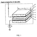
- Figure 1 shows a cell (1) of a light modulator with a deformable gel layer.
- the cell includes a first dielectric substrate layer (7) on which is mounted a first, or support, electrode (6) followed by the gel layer (5).
- a signal electrode (3) mounted on a second dielectric substrate layer (2) is separated from the deformable gel layer (5) by a second deformable layer (4) which in this case is air.
- a support voltage unit (8) is also provided.
- Such a basic arrangement is described in Russian Patent 2080641 to Guscho et al.
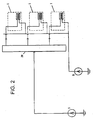
- Figure 2 shows an arrangement of several such cells connected in a light modulator.
- a bias voltage unit (9) is also provided for the signals.
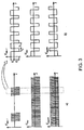
- Figure 3 shows time dependencies of the voltage at the i - th signal electrode, U sign.i , and at the outlets of the bias voltage ( U bias ) and support voltage ( U support. ) units.
- U bias bias voltage
- U support. support voltage
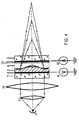
- a focusing system comprising the following components arranged in succession along the same optical axis: a light source (10), a condenser (11) and a lens (32).
- the system contains additionally a source of input electrical signals (18) and a transparent light modulator (14) with a deformable gel layer placed on the optical axis behind the lens (32) and consisting of the cell (1) with the deformable gel layer (5) and the support voltage unit (8).
- the signal electrode (3) is coated with a dielectric layer (33).
- the signal electrode (3) is connected with the source of input electrical signals (18) and the support electrode (6) is connected with the support voltage unit (8).
- the voltages applied to the signal (3) and support (6) electrodes can be constant or alternating and at any instant of time the polarity of voltage applied to the support electrode (6) will be opposite to the polarity of voltage applied to the signal electrode (3).
- the relief surface of the deformable gel layer (5) takes the shape of a lens.
- Different voltages may be applied to the signal electrodes of all cells (1) of the light modulator (14) so that the distribution of the electric potential across the plane of the signal electrodes (3) and at the interface between the deformable layers is not rastered, which ensures space-time control of the relief shape in accordance with a certain law.
- the signal electrode in the cell (1) of the light modulator (14) is in the form of concentric rings, each of the rings being connected with the outlet of its own switch device (41), as shown in Figure 5 .
- the size of the signal electrodes may reduce from the centre towards the periphery, as shown, but for a particular relief may remain constant or increase in this direction, or be irregular.
Landscapes
- Physics & Mathematics (AREA)
- General Physics & Mathematics (AREA)
- Optics & Photonics (AREA)
- Engineering & Computer Science (AREA)
- Multimedia (AREA)
- Signal Processing (AREA)
- Mechanical Light Control Or Optical Switches (AREA)
- Optical Communication System (AREA)
- Optical Couplings Of Light Guides (AREA)
- Electrochromic Elements, Electrophoresis, Or Variable Reflection Or Absorption Elements (AREA)
- Automatic Focus Adjustment (AREA)
- Color Television Image Signal Generators (AREA)
Claims (6)
- Système de focalisation comprenant un modulateur de lumière (14) comprenant une pluralité de cellules (1), chaque cellule comprenant deux couches diélectriques déformables (4, 5) qui se rencontrent à une interface, au moins l'une d'entre elles (5) étant un gel de formation de relief, une première électrode (6) d'un côté des couches et une électrode de signal (3) de l'autre côté des couches, ledit système de focalisation comprenant en outre des moyens (18) agencés pour fournir des signaux aux électrodes de signal des cellules de manière qu'une surface de relief de la couche de gel déformable prenne la forme d'une lentille de manière que le modulateur de lumière agisse comme une lentille, dans lequel les électrodes de signal (3) des cellules (1) sont agencées sous la forme d'anneaux concentriques commutables de manière indépendante (42).
- Système de focalisation selon la revendication 1, dans lequel les moyens (18) agencés pour fournir des signaux aux électrodes de signal (3) des cellules (1) sont agencés pour faire varier les signaux de manière à faire varier le profil du relief et modifier ainsi la longueur focale de la lentille (14) en changeant le rayon de courbure de la surface de couche de gel déformable.
- Système de focalisation selon la revendication 1, dans lequel des tensions différentes sont appliquées aux électrodes de signal des cellules de manière que la distribution du potentiel électrique à travers le plan des électrodes de signal et à l'interface entre les couches déformables ne soit pas tramé.
- Système de focalisation selon la revendication 1, dans lequel l'étendue radiale des électrodes de signal (42) diminue de l'anneau le plus interne à l'anneau le plus externe.
- Système de focalisation selon une quelconque revendication précédente, dans lequel les critères suivants sont remplis pour chaque cellule (1) :


- Système de focalisation selon une quelconque revendication précédente, dans lequel le gel de formation de relief est un gel de polyorganosiloxane.
Priority Applications (4)
| Application Number | Priority Date | Filing Date | Title |
|---|---|---|---|
| EP10010515.4A EP2278385B1 (fr) | 1999-12-23 | 2000-12-22 | Systèmes optiques |
| EP10010513A EP2278379A3 (fr) | 1999-12-23 | 2000-12-22 | Systèmes optiques |
| EP10010516A EP2302439A1 (fr) | 1999-12-23 | 2000-12-22 | Systèmes optiques |
| EP10010514.7A EP2293134B1 (fr) | 1999-12-23 | 2000-12-22 | Systèmes optiques |
Applications Claiming Priority (2)
| Application Number | Priority Date | Filing Date | Title |
|---|---|---|---|
| GBGB9930555.9A GB9930555D0 (en) | 1999-12-23 | 1999-12-23 | Optical systems |
| EP00985693A EP1244928B1 (fr) | 1999-12-23 | 2000-12-22 | Systemes optiques |
Related Parent Applications (1)
| Application Number | Title | Priority Date | Filing Date |
|---|---|---|---|
| EP00985693A Division EP1244928B1 (fr) | 1999-12-23 | 2000-12-22 | Systemes optiques |
Related Child Applications (8)
| Application Number | Title | Priority Date | Filing Date |
|---|---|---|---|
| EP10010513A Division-Into EP2278379A3 (fr) | 1999-12-23 | 2000-12-22 | Systèmes optiques |
| EP10010514.7A Division EP2293134B1 (fr) | 1999-12-23 | 2000-12-22 | Systèmes optiques |
| EP10010514.7A Previously-Filed-Application EP2293134B1 (fr) | 1999-12-23 | 2000-12-22 | Systèmes optiques |
| EP10010514.7A Division-Into EP2293134B1 (fr) | 1999-12-23 | 2000-12-22 | Systèmes optiques |
| EP10010515.4A Division EP2278385B1 (fr) | 1999-12-23 | 2000-12-22 | Systèmes optiques |
| EP10010515.4A Previously-Filed-Application EP2278385B1 (fr) | 1999-12-23 | 2000-12-22 | Systèmes optiques |
| EP10010515.4A Division-Into EP2278385B1 (fr) | 1999-12-23 | 2000-12-22 | Systèmes optiques |
| EP10010516A Division-Into EP2302439A1 (fr) | 1999-12-23 | 2000-12-22 | Systèmes optiques |
Publications (3)
| Publication Number | Publication Date |
|---|---|
| EP2000828A2 EP2000828A2 (fr) | 2008-12-10 |
| EP2000828A3 EP2000828A3 (fr) | 2009-02-25 |
| EP2000828B1 true EP2000828B1 (fr) | 2016-08-17 |
Family
ID=10866977
Family Applications (6)
| Application Number | Title | Priority Date | Filing Date |
|---|---|---|---|
| EP08016546.7A Expired - Lifetime EP2000828B1 (fr) | 1999-12-23 | 2000-12-22 | Système de focalisation comprenant un modulateur de lumière |
| EP10010515.4A Expired - Lifetime EP2278385B1 (fr) | 1999-12-23 | 2000-12-22 | Systèmes optiques |
| EP10010516A Withdrawn EP2302439A1 (fr) | 1999-12-23 | 2000-12-22 | Systèmes optiques |
| EP00985693A Expired - Lifetime EP1244928B1 (fr) | 1999-12-23 | 2000-12-22 | Systemes optiques |
| EP10010513A Withdrawn EP2278379A3 (fr) | 1999-12-23 | 2000-12-22 | Systèmes optiques |
| EP10010514.7A Expired - Lifetime EP2293134B1 (fr) | 1999-12-23 | 2000-12-22 | Systèmes optiques |
Family Applications After (5)
| Application Number | Title | Priority Date | Filing Date |
|---|---|---|---|
| EP10010515.4A Expired - Lifetime EP2278385B1 (fr) | 1999-12-23 | 2000-12-22 | Systèmes optiques |
| EP10010516A Withdrawn EP2302439A1 (fr) | 1999-12-23 | 2000-12-22 | Systèmes optiques |
| EP00985693A Expired - Lifetime EP1244928B1 (fr) | 1999-12-23 | 2000-12-22 | Systemes optiques |
| EP10010513A Withdrawn EP2278379A3 (fr) | 1999-12-23 | 2000-12-22 | Systèmes optiques |
| EP10010514.7A Expired - Lifetime EP2293134B1 (fr) | 1999-12-23 | 2000-12-22 | Systèmes optiques |
Country Status (7)
| Country | Link |
|---|---|
| EP (6) | EP2000828B1 (fr) |
| AT (1) | ATE409883T1 (fr) |
| AU (1) | AU2209201A (fr) |
| DE (1) | DE60040414D1 (fr) |
| DK (1) | DK1244928T3 (fr) |
| GB (1) | GB9930555D0 (fr) |
| WO (1) | WO2001048531A2 (fr) |
Families Citing this family (12)
| Publication number | Priority date | Publication date | Assignee | Title |
|---|---|---|---|---|
| ATE406599T1 (de) * | 2002-06-13 | 2008-09-15 | Nokia Corp | Erweiterungselektrodenkonfiguration für elektrisch gesteuerte lichtmodulatoren |
| JP2005525604A (ja) | 2002-09-06 | 2005-08-25 | フォトニックス アーエス | 可変光減衰器の方法及びデバイス |
| RU2230348C1 (ru) * | 2002-12-27 | 2004-06-10 | Гущо Юрий Петрович | Электрооптический преобразователь, гелеобразный слой для электрооптического преобразователя, способ приготовления гелеобразного слоя (варианты) и композиция для осуществления способа |
| AU2003258743A1 (en) | 2003-08-29 | 2005-03-16 | Nokia Corporation | Electrical device utilizing charge recycling within a cell |
| NO20054834D0 (no) * | 2005-10-19 | 2005-10-19 | Ignis Photonyx As | Lysmodulator for skannede linjeprojeksjonssystem |
| NO327026B1 (no) * | 2005-12-06 | 2009-04-06 | Ignis Display As | Fremgangsmate for a oke overflateledningsevnen av en polymer anvendt i en modulator med innstillbart diffraksjonsgitter (TDG) |
| NO20055796D0 (no) * | 2005-12-07 | 2005-12-07 | Ignis Photonyx As | Linjeskanningsprojeksjonsfremvisningssystem innbefattende en dobbel pixelradlysmodulator |
| GB2438458A (en) | 2006-05-11 | 2007-11-28 | Univ Cambridge Tech | Blocking zero-order light in phase shift hologram generation |
| JP2009539143A (ja) | 2006-06-01 | 2009-11-12 | ライト レゾナンス テクノロジーズ リミテッド ライアビリティー カンパニー | 光フィルタ/モジュレータ及びフィルタ/モジュレータのアレイ |
| KR20090099542A (ko) * | 2006-12-04 | 2009-09-22 | 포라이트 에이에스 | 모듈레이터 장치 및 3차원 디스플레이 시스템용 장치 |
| JP7246068B2 (ja) * | 2017-12-28 | 2023-03-27 | 国立大学法人信州大学 | 光学素子、及び光学素子の作製方法 |
| JP7341645B2 (ja) * | 2018-09-21 | 2023-09-11 | デクセリアルズ株式会社 | 光学体の製造方法 |
Family Cites Families (20)
| Publication number | Priority date | Publication date | Assignee | Title |
|---|---|---|---|---|
| US1229646A (en) | 1912-08-31 | 1917-06-12 | Recording And Computing Machines Company | Fare-recording mechanism. |
| NL163740B (nl) * | 1950-09-04 | Hydro Ban Corp | Als dakbedekking geschikt laminaat uit een voor vloei- stof ondoordringbaar synthetisch polymeer en een elastomeer materiaal. | |
| US2896507A (en) * | 1952-04-16 | 1959-07-28 | Foerderung Forschung Gmbh | Arrangement for amplifying the light intensity of an optically projected image |
| CH424009A (de) * | 1965-06-24 | 1966-11-15 | Foerderung Forschung Gmbh | Einrichtung zur Verstärkung der Intensität eines optisch erzeugten Bildes |
| SU678519A1 (ru) * | 1977-07-25 | 1979-08-05 | Московский институт радиотехники, электроники и автоматики | Устройство дл оптической записи и воспроизведени |
| DE3062778D1 (en) * | 1979-11-08 | 1983-05-19 | Gretag Ag | Optical image intensifier |
| US4466703A (en) * | 1981-03-24 | 1984-08-21 | Canon Kabushiki Kaisha | Variable-focal-length lens using an electrooptic effect |
| US4626920A (en) | 1984-01-30 | 1986-12-02 | New York Institute Of Technology | Solid state light modulator structure |
| US4857978A (en) | 1987-08-11 | 1989-08-15 | North American Philips Corporation | Solid state light modulator incorporating metallized gel and method of metallization |
| US4900136A (en) | 1987-08-11 | 1990-02-13 | North American Philips Corporation | Method of metallizing silica-containing gel and solid state light modulator incorporating the metallized gel |
| JPH01120502A (ja) * | 1987-11-05 | 1989-05-12 | Sanyo Electric Co Ltd | 焦点調整装置 |
| JPH01140118A (ja) * | 1987-11-27 | 1989-06-01 | Mitsubishi Heavy Ind Ltd | 焦点距離可変レンズ |
| US5097352A (en) * | 1988-09-28 | 1992-03-17 | Olympus Optical Co., Ltd. | Optical system including liquid crystal devices |
| US5751261A (en) * | 1990-12-31 | 1998-05-12 | Kopin Corporation | Control system for display panels |
| RU2031624C1 (ru) * | 1992-01-31 | 1995-03-27 | Юрий Петрович Гущо | Рельефографическое устройство для записи информации |
| JPH0750204B2 (ja) * | 1993-02-19 | 1995-05-31 | 名古屋大学長 | 高分子ゲルレンズの焦点距離制御方法及びそれを利用した鮮明な映像の結像方法 |
| RU2080624C1 (ru) | 1993-05-20 | 1997-05-27 | Виктор Константинович Ляпидевский | Устройство для измерения потоков незаряженных частиц и квантов |
| RU2078478C1 (ru) | 1994-04-18 | 1997-04-27 | Юрий Петрович Гущо | Устройство для записи и воспроизведения информации |
| US5920418A (en) * | 1994-06-21 | 1999-07-06 | Matsushita Electric Industrial Co., Ltd. | Diffractive optical modulator and method for producing the same, infrared sensor including such a diffractive optical modulator and method for producing the same, and display device including such a diffractive optical modulator |
| RU2080641C1 (ru) * | 1995-06-28 | 1997-05-27 | Малое индивидуальное предприятие "Кольцо" | Телевизионный проектор |
-
1999
- 1999-12-23 GB GBGB9930555.9A patent/GB9930555D0/en not_active Ceased
-
2000
- 2000-12-22 EP EP08016546.7A patent/EP2000828B1/fr not_active Expired - Lifetime
- 2000-12-22 EP EP10010515.4A patent/EP2278385B1/fr not_active Expired - Lifetime
- 2000-12-22 AU AU22092/01A patent/AU2209201A/en not_active Abandoned
- 2000-12-22 DE DE60040414T patent/DE60040414D1/de not_active Expired - Lifetime
- 2000-12-22 AT AT00985693T patent/ATE409883T1/de not_active IP Right Cessation
- 2000-12-22 EP EP10010516A patent/EP2302439A1/fr not_active Withdrawn
- 2000-12-22 DK DK00985693T patent/DK1244928T3/da active
- 2000-12-22 EP EP00985693A patent/EP1244928B1/fr not_active Expired - Lifetime
- 2000-12-22 WO PCT/GB2000/004987 patent/WO2001048531A2/fr not_active Ceased
- 2000-12-22 EP EP10010513A patent/EP2278379A3/fr not_active Withdrawn
- 2000-12-22 EP EP10010514.7A patent/EP2293134B1/fr not_active Expired - Lifetime
Also Published As
| Publication number | Publication date |
|---|---|
| EP2278379A2 (fr) | 2011-01-26 |
| EP2000828A2 (fr) | 2008-12-10 |
| EP2000828A3 (fr) | 2009-02-25 |
| EP2278385A3 (fr) | 2011-03-02 |
| EP1244928A2 (fr) | 2002-10-02 |
| EP2278385A2 (fr) | 2011-01-26 |
| WO2001048531A3 (fr) | 2002-01-17 |
| EP2293134B1 (fr) | 2014-07-16 |
| EP2278379A3 (fr) | 2011-03-02 |
| AU2209201A (en) | 2001-07-09 |
| DE60040414D1 (de) | 2008-11-13 |
| GB9930555D0 (en) | 2000-02-16 |
| ATE409883T1 (de) | 2008-10-15 |
| WO2001048531A2 (fr) | 2001-07-05 |
| EP2278385B1 (fr) | 2014-07-16 |
| DK1244928T3 (da) | 2009-02-02 |
| EP2302439A1 (fr) | 2011-03-30 |
| EP1244928B1 (fr) | 2008-10-01 |
| EP2293134A1 (fr) | 2011-03-09 |
Similar Documents
| Publication | Publication Date | Title |
|---|---|---|
| EP2000828B1 (fr) | Système de focalisation comprenant un modulateur de lumière | |
| Neil et al. | Dynamic wave-front generation for the characterization and testing of optical systems | |
| JP4154858B2 (ja) | 可変焦点レンズ | |
| US2155660A (en) | Light modulating device | |
| EP0992833A3 (fr) | Appareil pour le contrôle de la transmission de lumière par films métalliques perforés avec des trous de diamètre à sous-multiples de la longueur d'onde | |
| JPH01120502A (ja) | 焦点調整装置 | |
| EP1580592B1 (fr) | Appareil de projection d'images avec CONVERTISSEUR ELECTRO-OPTIQUE, COUCHE GELIFORME DESTINEE AUDIT CONVERTISSEUR ELECTRO-OPTIQUE, PROCEDE DE FABRICATION DE LADITE COUCHE GELIFORME ET COMPOSITION DESTINEE A METTRE EN OEUVRE LE PROCEDE CORRESPONDANT | |
| KR910021161A (ko) | 칼라 비디오 영상 투사 장치 | |
| Tong et al. | Combination of micro-scanning mirrors and multi-mode fibers for speckle reduction in high lumen laser projector applications | |
| Niederriter et al. | Electrowetting lenses for compensating phase and curvature distortion in arrayed laser systems | |
| US4106848A (en) | Elastomer wave guide optical modulators | |
| EP0867743A3 (fr) | Modulateur à fibre optique comprenant une section polarisée fonctionnant comme élément électro-optique et procédé de fabrication | |
| Sakarya et al. | Spatial light modulators based on micromachined reflective membranes on viscoelastic layers | |
| Doyle et al. | Remote real-time reconstruction of holograms using the Lumatron | |
| US4815799A (en) | Infrared crystalline spatial light modulator | |
| Duerr et al. | MEMS Spatial Light Modulators for Real Holographic 3D Displays | |
| Lea | Optical modulators based on electrocapillarity | |
| Greenlee et al. | Electro-optic polymer spatial light modulator based on a Fabry–Perot interferometer configuration | |
| Rosenthal | Color control by ultrasonic wave gratings | |
| RU2134440C1 (ru) | Жидкокристаллический пространственно-временной модулятор света для систем оптической обработки информации | |
| Pizolato Jr et al. | Zeroth-order phase-contrast technique | |
| Zhao et al. | Novel photonic infrared scene generation technique | |
| Kuhlow et al. | Calculation of the optical transfer function of a light valve system with dark field observation | |
| SU1269086A1 (ru) | Растр | |
| RU1841109C (ru) | Мембранное зеркало |
Legal Events
| Date | Code | Title | Description |
|---|---|---|---|
| PUAI | Public reference made under article 153(3) epc to a published international application that has entered the european phase |
Free format text: ORIGINAL CODE: 0009012 |
|
| AC | Divisional application: reference to earlier application |
Ref document number: 1244928 Country of ref document: EP Kind code of ref document: P |
|
| AK | Designated contracting states |
Kind code of ref document: A2 Designated state(s): AT BE CH CY DE DK ES FI FR GB GR IE IT LI LU MC NL PT SE TR |
|
| PUAL | Search report despatched |
Free format text: ORIGINAL CODE: 0009013 |
|
| AK | Designated contracting states |
Kind code of ref document: A3 Designated state(s): AT BE CH CY DE DK ES FI FR GB GR IE IT LI LU MC NL PT SE TR |
|
| AKX | Designation fees paid |
Designated state(s): AT BE CH CY DE DK ES FI FR GB GR IE IT LI LU MC NL PT SE TR |
|
| 17Q | First examination report despatched |
Effective date: 20091001 |
|
| 17P | Request for examination filed |
Effective date: 20090825 |
|
| REG | Reference to a national code |
Ref country code: DE Ref legal event code: R079 Ref document number: 60049422 Country of ref document: DE Free format text: PREVIOUS MAIN CLASS: G02B0003140000 Ipc: G02B0026080000 |
|
| GRAP | Despatch of communication of intention to grant a patent |
Free format text: ORIGINAL CODE: EPIDOSNIGR1 |
|
| RIC1 | Information provided on ipc code assigned before grant |
Ipc: H04N 9/31 20060101ALI20160204BHEP Ipc: G02B 26/08 20060101AFI20160204BHEP Ipc: G02B 27/54 20060101ALI20160204BHEP |
|
| INTG | Intention to grant announced |
Effective date: 20160223 |
|
| GRAS | Grant fee paid |
Free format text: ORIGINAL CODE: EPIDOSNIGR3 |
|
| GRAA | (expected) grant |
Free format text: ORIGINAL CODE: 0009210 |
|
| AC | Divisional application: reference to earlier application |
Ref document number: 1244928 Country of ref document: EP Kind code of ref document: P |
|
| AK | Designated contracting states |
Kind code of ref document: B1 Designated state(s): AT BE CH CY DE DK ES FI FR GB GR IE IT LI LU MC NL PT SE TR |
|
| REG | Reference to a national code |
Ref country code: GB Ref legal event code: FG4D |
|
| REG | Reference to a national code |
Ref country code: CH Ref legal event code: EP |
|
| REG | Reference to a national code |
Ref country code: IE Ref legal event code: FG4D |
|
| REG | Reference to a national code |
Ref country code: AT Ref legal event code: REF Ref document number: 821618 Country of ref document: AT Kind code of ref document: T Effective date: 20160915 |
|
| REG | Reference to a national code |
Ref country code: DE Ref legal event code: R096 Ref document number: 60049422 Country of ref document: DE |
|
| REG | Reference to a national code |
Ref country code: NL Ref legal event code: MP Effective date: 20160817 |
|
| REG | Reference to a national code |
Ref country code: AT Ref legal event code: MK05 Ref document number: 821618 Country of ref document: AT Kind code of ref document: T Effective date: 20160817 |
|
| PG25 | Lapsed in a contracting state [announced via postgrant information from national office to epo] |
Ref country code: FI Free format text: LAPSE BECAUSE OF FAILURE TO SUBMIT A TRANSLATION OF THE DESCRIPTION OR TO PAY THE FEE WITHIN THE PRESCRIBED TIME-LIMIT Effective date: 20160817 Ref country code: NL Free format text: LAPSE BECAUSE OF FAILURE TO SUBMIT A TRANSLATION OF THE DESCRIPTION OR TO PAY THE FEE WITHIN THE PRESCRIBED TIME-LIMIT Effective date: 20160817 Ref country code: IT Free format text: LAPSE BECAUSE OF FAILURE TO SUBMIT A TRANSLATION OF THE DESCRIPTION OR TO PAY THE FEE WITHIN THE PRESCRIBED TIME-LIMIT Effective date: 20160817 |
|
| PG25 | Lapsed in a contracting state [announced via postgrant information from national office to epo] |
Ref country code: GR Free format text: LAPSE BECAUSE OF FAILURE TO SUBMIT A TRANSLATION OF THE DESCRIPTION OR TO PAY THE FEE WITHIN THE PRESCRIBED TIME-LIMIT Effective date: 20161118 Ref country code: ES Free format text: LAPSE BECAUSE OF FAILURE TO SUBMIT A TRANSLATION OF THE DESCRIPTION OR TO PAY THE FEE WITHIN THE PRESCRIBED TIME-LIMIT Effective date: 20160817 Ref country code: PT Free format text: LAPSE BECAUSE OF FAILURE TO SUBMIT A TRANSLATION OF THE DESCRIPTION OR TO PAY THE FEE WITHIN THE PRESCRIBED TIME-LIMIT Effective date: 20161219 Ref country code: AT Free format text: LAPSE BECAUSE OF FAILURE TO SUBMIT A TRANSLATION OF THE DESCRIPTION OR TO PAY THE FEE WITHIN THE PRESCRIBED TIME-LIMIT Effective date: 20160817 Ref country code: SE Free format text: LAPSE BECAUSE OF FAILURE TO SUBMIT A TRANSLATION OF THE DESCRIPTION OR TO PAY THE FEE WITHIN THE PRESCRIBED TIME-LIMIT Effective date: 20160817 |
|
| REG | Reference to a national code |
Ref country code: DE Ref legal event code: R097 Ref document number: 60049422 Country of ref document: DE |
|
| PG25 | Lapsed in a contracting state [announced via postgrant information from national office to epo] |
Ref country code: DK Free format text: LAPSE BECAUSE OF FAILURE TO SUBMIT A TRANSLATION OF THE DESCRIPTION OR TO PAY THE FEE WITHIN THE PRESCRIBED TIME-LIMIT Effective date: 20160817 Ref country code: BE Free format text: LAPSE BECAUSE OF FAILURE TO SUBMIT A TRANSLATION OF THE DESCRIPTION OR TO PAY THE FEE WITHIN THE PRESCRIBED TIME-LIMIT Effective date: 20160817 |
|
| PLBE | No opposition filed within time limit |
Free format text: ORIGINAL CODE: 0009261 |
|
| STAA | Information on the status of an ep patent application or granted ep patent |
Free format text: STATUS: NO OPPOSITION FILED WITHIN TIME LIMIT |
|
| REG | Reference to a national code |
Ref country code: DE Ref legal event code: R119 Ref document number: 60049422 Country of ref document: DE |
|
| 26N | No opposition filed |
Effective date: 20170518 |
|
| REG | Reference to a national code |
Ref country code: CH Ref legal event code: PL |
|
| GBPC | Gb: european patent ceased through non-payment of renewal fee |
Effective date: 20161222 |
|
| PG25 | Lapsed in a contracting state [announced via postgrant information from national office to epo] |
Ref country code: MC Free format text: LAPSE BECAUSE OF FAILURE TO SUBMIT A TRANSLATION OF THE DESCRIPTION OR TO PAY THE FEE WITHIN THE PRESCRIBED TIME-LIMIT Effective date: 20160817 |
|
| REG | Reference to a national code |
Ref country code: FR Ref legal event code: ST Effective date: 20170831 |
|
| REG | Reference to a national code |
Ref country code: IE Ref legal event code: MM4A |
|
| PG25 | Lapsed in a contracting state [announced via postgrant information from national office to epo] |
Ref country code: FR Free format text: LAPSE BECAUSE OF NON-PAYMENT OF DUE FEES Effective date: 20170102 Ref country code: LI Free format text: LAPSE BECAUSE OF NON-PAYMENT OF DUE FEES Effective date: 20161231 Ref country code: LU Free format text: LAPSE BECAUSE OF NON-PAYMENT OF DUE FEES Effective date: 20161222 Ref country code: CH Free format text: LAPSE BECAUSE OF NON-PAYMENT OF DUE FEES Effective date: 20161231 |
|
| PG25 | Lapsed in a contracting state [announced via postgrant information from national office to epo] |
Ref country code: DE Free format text: LAPSE BECAUSE OF NON-PAYMENT OF DUE FEES Effective date: 20170701 Ref country code: GB Free format text: LAPSE BECAUSE OF NON-PAYMENT OF DUE FEES Effective date: 20161222 Ref country code: IE Free format text: LAPSE BECAUSE OF NON-PAYMENT OF DUE FEES Effective date: 20161222 |
|
| PG25 | Lapsed in a contracting state [announced via postgrant information from national office to epo] |
Ref country code: CY Free format text: LAPSE BECAUSE OF FAILURE TO SUBMIT A TRANSLATION OF THE DESCRIPTION OR TO PAY THE FEE WITHIN THE PRESCRIBED TIME-LIMIT Effective date: 20160817 |
|
| PG25 | Lapsed in a contracting state [announced via postgrant information from national office to epo] |
Ref country code: TR Free format text: LAPSE BECAUSE OF FAILURE TO SUBMIT A TRANSLATION OF THE DESCRIPTION OR TO PAY THE FEE WITHIN THE PRESCRIBED TIME-LIMIT Effective date: 20160817 |