EP2000007B1 - Pulse width modulation based led dimmer control - Google Patents
Pulse width modulation based led dimmer control Download PDFInfo
- Publication number
- EP2000007B1 EP2000007B1 EP07735197A EP07735197A EP2000007B1 EP 2000007 B1 EP2000007 B1 EP 2000007B1 EP 07735197 A EP07735197 A EP 07735197A EP 07735197 A EP07735197 A EP 07735197A EP 2000007 B1 EP2000007 B1 EP 2000007B1
- Authority
- EP
- European Patent Office
- Prior art keywords
- pulse width
- dimmer
- led
- group
- control
- Prior art date
- Legal status (The legal status is an assumption and is not a legal conclusion. Google has not performed a legal analysis and makes no representation as to the accuracy of the status listed.)
- Not-in-force
Links
Images

Classifications
-
- H—ELECTRICITY
- H05—ELECTRIC TECHNIQUES NOT OTHERWISE PROVIDED FOR
- H05B—ELECTRIC HEATING; ELECTRIC LIGHT SOURCES NOT OTHERWISE PROVIDED FOR; CIRCUIT ARRANGEMENTS FOR ELECTRIC LIGHT SOURCES, IN GENERAL
- H05B45/00—Circuit arrangements for operating light-emitting diodes [LED]
- H05B45/30—Driver circuits
- H05B45/37—Converter circuits
- H05B45/3725—Switched mode power supply [SMPS]
-
- H—ELECTRICITY
- H05—ELECTRIC TECHNIQUES NOT OTHERWISE PROVIDED FOR
- H05B—ELECTRIC HEATING; ELECTRIC LIGHT SOURCES NOT OTHERWISE PROVIDED FOR; CIRCUIT ARRANGEMENTS FOR ELECTRIC LIGHT SOURCES, IN GENERAL
- H05B45/00—Circuit arrangements for operating light-emitting diodes [LED]
- H05B45/20—Controlling the colour of the light
-
- H—ELECTRICITY
- H05—ELECTRIC TECHNIQUES NOT OTHERWISE PROVIDED FOR
- H05B—ELECTRIC HEATING; ELECTRIC LIGHT SOURCES NOT OTHERWISE PROVIDED FOR; CIRCUIT ARRANGEMENTS FOR ELECTRIC LIGHT SOURCES, IN GENERAL
- H05B45/00—Circuit arrangements for operating light-emitting diodes [LED]
- H05B45/10—Controlling the intensity of the light
-
- H—ELECTRICITY
- H05—ELECTRIC TECHNIQUES NOT OTHERWISE PROVIDED FOR
- H05B—ELECTRIC HEATING; ELECTRIC LIGHT SOURCES NOT OTHERWISE PROVIDED FOR; CIRCUIT ARRANGEMENTS FOR ELECTRIC LIGHT SOURCES, IN GENERAL
- H05B45/00—Circuit arrangements for operating light-emitting diodes [LED]
- H05B45/20—Controlling the colour of the light
- H05B45/24—Controlling the colour of the light using electrical feedback from LEDs or from LED modules
-
- H—ELECTRICITY
- H05—ELECTRIC TECHNIQUES NOT OTHERWISE PROVIDED FOR
- H05B—ELECTRIC HEATING; ELECTRIC LIGHT SOURCES NOT OTHERWISE PROVIDED FOR; CIRCUIT ARRANGEMENTS FOR ELECTRIC LIGHT SOURCES, IN GENERAL
- H05B47/00—Circuit arrangements for operating light sources in general, i.e. where the type of light source is not relevant
- H05B47/10—Controlling the light source
- H05B47/175—Controlling the light source by remote control
- H05B47/18—Controlling the light source by remote control via data-bus transmission
- H05B47/183—Controlling the light source by remote control via data-bus transmission using digital addressable lighting interface [DALI] communication protocols
-
- F—MECHANICAL ENGINEERING; LIGHTING; HEATING; WEAPONS; BLASTING
- F21—LIGHTING
- F21Y—INDEXING SCHEME ASSOCIATED WITH SUBCLASSES F21K, F21L, F21S and F21V, RELATING TO THE FORM OR THE KIND OF THE LIGHT SOURCES OR OF THE COLOUR OF THE LIGHT EMITTED
- F21Y2115/00—Light-generating elements of semiconductor light sources
- F21Y2115/10—Light-emitting diodes [LED]
-
- Y—GENERAL TAGGING OF NEW TECHNOLOGICAL DEVELOPMENTS; GENERAL TAGGING OF CROSS-SECTIONAL TECHNOLOGIES SPANNING OVER SEVERAL SECTIONS OF THE IPC; TECHNICAL SUBJECTS COVERED BY FORMER USPC CROSS-REFERENCE ART COLLECTIONS [XRACs] AND DIGESTS
- Y02—TECHNOLOGIES OR APPLICATIONS FOR MITIGATION OR ADAPTATION AGAINST CLIMATE CHANGE
- Y02B—CLIMATE CHANGE MITIGATION TECHNOLOGIES RELATED TO BUILDINGS, e.g. HOUSING, HOUSE APPLIANCES OR RELATED END-USER APPLICATIONS
- Y02B20/00—Energy efficient lighting technologies, e.g. halogen lamps or gas discharge lamps
- Y02B20/30—Semiconductor lamps, e.g. solid state lamps [SSL] light emitting diodes [LED] or organic LED [OLED]
Definitions
- the present invention relates generally to methods and apparatus for LED dimmer control.
- the present invention more particularly relates to circuits and methods for providing pulse width modulated dimmer control for LEDs, dimming operations with multiple LEDs of different colors, and communicating dimmer control information between clock domains without introducing visual artifacts.
- LEDs have evolved relatively quickly since their introduction, and are now widely used in product areas including consumer and industrial electronics, as well as in lighting applications. Some of the improvements have been in areas such as brightness, and the availability of a variety of colors. Other advances have come in terms of applications for these useful lighting elements, and in the circuits used to control them.
- a synchronization protocol is used to allow control information for the dimmer operations to be transferred to the PWM dimmer control clock domain from an external clock domain, such that visual artifacts are prevented when the control information is updated.
- control information is transferred to the LED dimmer controller via an I2C serial bus, and the synchronization protocol waits for an I2C STOP condition before updating control information across clock domain boundaries.
- the leading and trailing edges of an asserted group dimmer control signal are generated such that the active portion of the group dimmer control signal overlaps the active portion of individual LED pulse width modulated control signals. In this way, the pulse width modulation of the individual LED control signals is not cut off, or reduced in width by the group dimmer signal.
- the present invention relates to LED dimmer controls.
- Various aspects of the present invention relate more particularly to circuits and methods for providing pulse width modulated dimmer control for LEDs, dimming operations with multiple LEDs of different colors, and communicating dimmer control information between clock domains without introducing visual artifacts.
- integrated circuit integrated circuit
- IC integrated circuit
- chip chip, die, semiconductor device
- monolithic integrated circuit microelectronic device
- microelectronic device and similar variants may be used interchangeably herein.
- signals are coupled between them and other circuit elements, including but not limited to other microelectronic devices, via physical, electrically conductive connections.
- the point of connection is sometimes referred to as an input, output, input/output (I/O), terminal, line, pin, pad, port, interface, or similar variants and combinations. Unless specifically noted in the context of use, these are considered equivalent terms for the purpose of this disclosure.
- Various embodiments of the present invention provide systems and methods to cleanly control the dimming of LEDs, both individually and as a group, using pulse width modulation, and without producing visual artifacts from such dimming control.
- Pulse width modulation is an efficient way of controlling LEDs.
- the human eye averages the brightness of the different color LEDs thereby creating the perception of seeing different colors.
- pulsing electrical current through the LEDs at a high enough frequency typically greater than 2kHz
- LED dimmer controllers provide for dimming LEDs without producing various undesirable visual artifacts.
- an LED dimmer controller in accordance with the invention avoids visual artifacts such as sudden flashes of light during the dimming process; and avoids chopping off the original waveform with the dimming waveform and accordingly avoids visual artifacts such as changing the original brightness of an LED.
- a pulse width modulated LED dimmer controller typically includes registers that are capable of being controlled, or accessed, from the external world. In typical applications for LED lighting products equipped with pulse width modulated LED dimmers, it is preferable that access to the registers of the dimmer be by a simple mechanism. In an illustrative embodiment of the present invention, which is described below, an I12C serial bus interface is used for providing access to these registers. It is noted that, in this scenario, an LED dimmer resides on a first chip, and control information is sent to the first chip from a second chip, via an I2C serial bus.
- the illustrative embodiment uses an on-chip oscillator to provide the pulse width modulation (PWM) circuit with the required base clock frequency that is used to achieve the pulse width modulation of the dimmer control signals.
- Pulse width modulation of these dimmer control signals may be achieved by completely synchronous logic including counters and comparators.
- control circuits for both the individual and group dimming operations are implemented in an integrated circuit and include various registers internal to that integrated circuit. In order to specify various brightness and dimming control parameters, a user may cause information to be written to those internal registers, which in turn, controls the individual LED dimming PWM, and the group LED dimming PWM circuits.
- the writes, or data transfers, to the internal registers are done via an I2C serial interface that is mostly synchronous, i.e., except for the asynchronous Start and Stop conditions of the I2C protocol.
- I2C serial interface that is mostly synchronous, i.e., except for the asynchronous Start and Stop conditions of the I2C protocol.
- SCL clock domain defined by the I2C master device
- an internal oscillator generates a base clock, which is divided and used in the individual and group PWM circuits, thereby creating an oscillator (OSC) clock domain.
- OSC oscillator
- embodiments of the present invention advantageously ensure that clean control parameter updates result in LED outputs without visual artifacts being detected by an observer.
- FIG. 1 shows an illustrative embodiment of the present invention.
- An oscillator 102 provides a clock signal to an 8-bit counter 104.
- the clock signal of oscillator 102 is further coupled the clock input terminals of comparators Pwm0 106, Pwm 1 108, Pwm2 110, and Pwm3 112.
- Comparators Pwm0 106, Pwm 1108, Pwm2 110, and Pwm3 112 are further coupled in common to receive an output signal from 8-bit counter 104.
- comparators Pwm0 106, Pwm 1108, Pwm2 110, and Pwm3 112 are coupled to receive, respectively, the outputs from registers Pwm0_reg, Pwm1_reg, Pwm2_reg, and Pwm3_reg (not shown).
- a clock divider 114 is coupled to receive the output signal of 8-bit counter 104. The output of clock divider 114 is coupled to 8-bit counter 118, and to comparator Pwm4 116. Comparator Pwm4 116 is further coupled to receive the output of control register Grppwm_reg (not shown), and to receive the output of 8-bit counter 118.
- a first AND gate 120 is coupled to receive the output of comparator Pwm0 106 and the output of comparator Pwm4 1 16; and produces an output signal LED0 for controlling a first LED.
- a second AND gate 122 is coupled to receive the output of comparator Pwm1 108 and the output of comparator Pwm4 116; and produces an output signal LED1 for controlling a second LED.
- a third AND gate 124 is coupled to receive the output of comparator Pwm2 110 and the output of comparator Pwm4 116; and produces an output signal LED2 for controlling a third LED.
- a fourth AND gate 126 is coupled to receive the output of comparator Pwm3 112 and the output of comparator Pwm4 116; and produces an output signal LED3 for controlling a fourth LED.
- each of the first second, third and fourth LEDs (not shown) emits a different color of light.
- this illustrative implementation has four individual PWMs (Pwm0 through Pwm3) for individual LED brightness control, and one group PWM (Pwm4) for group dimming. It is noted that instead of group dimming, the same techniques can be used to achieve individual dimming controls as well.
- the individual PWMs are clocked by different divided down versions of the OSC clock (which is derived from an internal oscillator in this illustrative embodiment).
- the individual brightness control for the four LEDs is achieved by the user changing the values of Pwm0_reg through Pwm3_reg. Register writes occur through an I2C interface front end in this example.
- the group dimming control can be achieved by changing the value of the register Pwm4_reg.
- the I2C protocol which is a master/slave protocol, uses one line for serial data, which is well-known as SDA, and one line for a serial clock, which is well-known as SCL.
- SDA serial data
- SCL serial clock
- the I2C master device produces the SCL clock signal.
- the I2C protocol specifies timing, addressing, clocking, data transfer, acknowledgments, voltage levels, and so on
- the I2C clock Serial Clock (SCL)
- SCL Serial Clock
- the SCL signal can be stopped and started at any time by the I2C master device.
- data on the SDA line must be valid when the clock signal on the SCL line is high, with two exceptions.
- a high-to-low transition on the SDA line while the clock signal on the SCL line is high is interpreted as a "START” condition.
- a low-to-high transition on the SDA line while the clock signal on the SCL line is high is interpreted as a "STOP" condition.
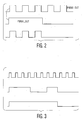
- Fig. 2 illustrates the basic timing waveforms for the dimmer control.
- the first waveform is the output of the individual PWM.
- the second waveform is the output of the group dimmer PWM.
- the third waveform is the resultant dimming waveform.
- the operation of the LED dimmer controller can be seen from an inspection of the waveforms shown in Fig. 2 . Due to the group dimmer signal, the resultant waveform has different ON and OFF times. This change in the average brightness of the LED is perceived by the human eye, which does an averaging operation, as dimming. It can be seen that by changing the value of the Pwm4_reg, the pulse width modulated output of the group PWM can be changed, which enables control of the resultant waveform, and hence provides for control of dimming the LED outputs.
- an LED dimmer controller in accordance with the invention must take into account factors such as, but not limited to, the following: the user interface operates at a different frequency (SCL clock domain) from the PWM frequency (OSC clock domain), hence there needs to be a clean handshake between these two clock domains; and the process of updating the LED outputs should be a smooth one rather than an abrupt one. The resulting update should happen so cleanly that the human eye does not perceive an abrupt switch.
- a method of updating all the LEDs together is provided by a mechanism referred to herein as "update on STOP".
- the actual update in the OSC clock domain is carefully controlled so that there are no visual artifacts resulting from the transfer of data across clock domain boundaries. This is achieved by a robust, synchronous, digital control mechanism.
- the illustrative PWM implementation is a counter/comparator implementation.
- a free running counter counts the number of clocks.
- a comparator compares the Pwm4_reg value with the counter to see if there is a match. If there is a match, then the Pwm4 output is asserted.
- a method for avoiding such visual artifacts includes determining that the Pwm4_reg in the SCL domain has been updated, and waiting for a STOP condition. Once the STOP condition occurs in the SCL clock domain, a clean clock boundary hand-shake across to the OSC clock domain is performed and a flag is set in the OSC clock domain. Subsequently, a wait state occurs until the Pwm4 counter in the OSC clock domain cleanly rolls over to zero. At this point in time, the Pwm4_reg shadow register in the OSC clock domain is updated to the new value. This procedure ensures that the new dim waveform is artifact-free.
- Fig. 3 illustrates the effect of following and not following the above-described procedure.
- various embodiments of the present invention include ensuring that the leading and trailing edges of the dimming waveform are separated in time from the original waveform.
- circuitry for this purpose. It will be further appreciated that careful attention is paid to the digital counter design and comparator design to ensure the edge separations described above are achieved.
- post-layout back annotated timing results should be analyzed to ensure that even after layout the above-described edge separations are valid.
- One advantage is that the visual artifacts, such as a flash of light during a dimming operation are eliminated.
- Another advantage is that synchronous digital designs in accordance with the present invention are verifiable through modern simulators and static timing analysis tools.
Landscapes
- Circuit Arrangement For Electric Light Sources In General (AREA)
- Led Devices (AREA)
Abstract
Description
- The present invention relates generally to methods and apparatus for LED dimmer control. The present invention more particularly relates to circuits and methods for providing pulse width modulated dimmer control for LEDs, dimming operations with multiple LEDs of different colors, and communicating dimmer control information between clock domains without introducing visual artifacts.
- There have been many advances in lighting technology since the introduction of the incandescent light bulb. One of the more recent advances in lighting technology has been the development of the light emitting diode, or LED, as it is more commonly referred to today. These semiconductor based lighting products have many desirable qualities, such as, for example, small size, operation from low voltage power supplies, and ease of integration with control cu-cuitry.
- LEDs have evolved relatively quickly since their introduction, and are now widely used in product areas including consumer and industrial electronics, as well as in lighting applications. Some of the improvements have been in areas such as brightness, and the availability of a variety of colors. Other advances have come in terms of applications for these useful lighting elements, and in the circuits used to control them.
- What is needed are methods and apparatus for providing LED dimmer controls that achieve the desired dimming while avoiding visual artifacts such as flashing during a dimming operation, and avoiding conventional circuit performance errors that affect LED brightness.
- Briefly, methods and apparatus for implementing and operating pulse width modulation based LED dimmer controllers are described.
- In one aspect of the present invention, a synchronization protocol is used to allow control information for the dimmer operations to be transferred to the PWM dimmer control clock domain from an external clock domain, such that visual artifacts are prevented when the control information is updated.
- In a further aspect of the present invention, control information is transferred to the LED dimmer controller via an I2C serial bus, and the synchronization protocol waits for an I2C STOP condition before updating control information across clock domain boundaries.
- In a still further aspect of the present invention, the leading and trailing edges of an asserted group dimmer control signal are generated such that the active portion of the group dimmer control signal overlaps the active portion of individual LED pulse width modulated control signals. In this way, the pulse width modulation of the individual LED control signals is not cut off, or reduced in width by the group dimmer signal.
-
Fig. 1 is a schematic block diagram of a circuit in accordance with the present invention. -
Fig. 2 is a timing diagram showing a pulse width modulated control signal for a single LED, a group-level dimming signal, and the resultant waveform and logically combining the first two signals to produce of dimmer output signal. -
Fig. 3 is a timing diagram showing the effects of following and not following the data transfer procedures in accordance with the present invention. - Generally, the present invention relates to LED dimmer controls. Various aspects of the present invention relate more particularly to circuits and methods for providing pulse width modulated dimmer control for LEDs, dimming operations with multiple LEDs of different colors, and communicating dimmer control information between clock domains without introducing visual artifacts.
- Reference herein to "one embodiment", "an embodiment", or similar formulations, means that a particular feature, structure, operation, or characteristic described in connection with the embodiment, is included in at least one embodiment of the present invention. Thus, the appearances of such phrases or formulations herein are not necessarily all referring to the same embodiment. Furthermore, various particular features, structures, operations, or characteristics may be combined in any suitable manner in one or more embodiments.
- The terms integrated circuit, IC, chip, die, semiconductor device, monolithic integrated circuit, microelectronic device, and similar variants may be used interchangeably herein. With respect to these microelectronic devices, signals are coupled between them and other circuit elements, including but not limited to other microelectronic devices, via physical, electrically conductive connections. The point of connection is sometimes referred to as an input, output, input/output (I/O), terminal, line, pin, pad, port, interface, or similar variants and combinations. Unless specifically noted in the context of use, these are considered equivalent terms for the purpose of this disclosure.
- Various embodiments of the present invention provide systems and methods to cleanly control the dimming of LEDs, both individually and as a group, using pulse width modulation, and without producing visual artifacts from such dimming control. Pulse width modulation is an efficient way of controlling LEDs. By varying the ON and OFF time of an LED, and using the various different color LEDs (e.g., R, G, B, and Y) that are now available, it is possible to create color mixing that is visible to the human eye. The human eye averages the brightness of the different color LEDs thereby creating the perception of seeing different colors. Further, by pulsing electrical current through the LEDs at a high enough frequency (typically greater than 2kHz) the human eye perceives a dimming effect.
- There are a number of challenges which are overcome by LED dimmer controllers in accordance with the present invention. Such LED dimmer controllers provide for dimming LEDs without producing various undesirable visual artifacts. For example, in addition to achieving the desired dimming of the LED outputs, an LED dimmer controller in accordance with the invention avoids visual artifacts such as sudden flashes of light during the dimming process; and avoids chopping off the original waveform with the dimming waveform and accordingly avoids visual artifacts such as changing the original brightness of an LED.
- A pulse width modulated LED dimmer controller (or simply LED dimmer) typically includes registers that are capable of being controlled, or accessed, from the external world. In typical applications for LED lighting products equipped with pulse width modulated LED dimmers, it is preferable that access to the registers of the dimmer be by a simple mechanism. In an illustrative embodiment of the present invention, which is described below, an I12C serial bus interface is used for providing access to these registers. It is noted that, in this scenario, an LED dimmer resides on a first chip, and control information is sent to the first chip from a second chip, via an I2C serial bus. Additionally, the illustrative embodiment uses an on-chip oscillator to provide the pulse width modulation (PWM) circuit with the required base clock frequency that is used to achieve the pulse width modulation of the dimmer control signals. Pulse width modulation of these dimmer control signals may be achieved by completely synchronous logic including counters and comparators.
- In the illustrative example described below, there are multiple LEDs each with a PWM control circuit for controlling the perceived brightness of that LED, as well as circuitry for dimming the LEDs as a group. The control circuits for both the individual and group dimming operations are implemented in an integrated circuit and include various registers internal to that integrated circuit. In order to specify various brightness and dimming control parameters, a user may cause information to be written to those internal registers, which in turn, controls the individual LED dimming PWM, and the group LED dimming PWM circuits.
- In the illustrative embodiment, the writes, or data transfers, to the internal registers are done via an I2C serial interface that is mostly synchronous, i.e., except for the asynchronous Start and Stop conditions of the I2C protocol. These write operations occur within the SCL clock domain (defined by the I2C master device), which is described in more detail below. Within the LED dimmer chip an internal oscillator generates a base clock, which is divided and used in the individual and group PWM circuits, thereby creating an oscillator (OSC) clock domain.
- When new values are written to the registers, embodiments of the present invention advantageously ensure that clean control parameter updates result in LED outputs without visual artifacts being detected by an observer.
- The block diagram of
Fig. 1 shows an illustrative embodiment of the present invention. Anoscillator 102 provides a clock signal to an 8-bit counter 104. The clock signal ofoscillator 102 is further coupled the clock input terminals ofcomparators Pwm0 106, Pwm 1 108,Pwm2 110, andPwm3 112.Comparators Pwm0 106, Pwm 1108,Pwm2 110, andPwm3 112 are further coupled in common to receive an output signal from 8-bit counter 104. Additionally,comparators Pwm0 106, Pwm 1108,Pwm2 110, andPwm3 112 are coupled to receive, respectively, the outputs from registers Pwm0_reg, Pwm1_reg, Pwm2_reg, and Pwm3_reg (not shown). Aclock divider 114 is coupled to receive the output signal of 8-bit counter 104. The output ofclock divider 114 is coupled to 8-bit counter 118, and tocomparator Pwm4 116.Comparator Pwm4 116 is further coupled to receive the output of control register Grppwm_reg (not shown), and to receive the output of 8-bit counter 118. Afirst AND gate 120 is coupled to receive the output ofcomparator Pwm0 106 and the output of comparator Pwm4 1 16; and produces an output signal LED0 for controlling a first LED. Asecond AND gate 122 is coupled to receive the output ofcomparator Pwm1 108 and the output ofcomparator Pwm4 116; and produces an output signal LED1 for controlling a second LED. Athird AND gate 124 is coupled to receive the output ofcomparator Pwm2 110 and the output ofcomparator Pwm4 116; and produces an output signal LED2 for controlling a third LED. Afourth AND gate 126 is coupled to receive the output ofcomparator Pwm3 112 and the output ofcomparator Pwm4 116; and produces an output signal LED3 for controlling a fourth LED. In this illustrative embodiment, each of the first second, third and fourth LEDs (not shown) emits a different color of light. - Those skilled in the art and having the benefit of this disclosure will recognize that alternative combinational logic and/or signal polarities may be used to achieve the illustrated functionality.
- Still referring to the block diagram of
Fig. 1 , this illustrative implementation has four individual PWMs (Pwm0 through Pwm3) for individual LED brightness control, and one group PWM (Pwm4) for group dimming. It is noted that instead of group dimming, the same techniques can be used to achieve individual dimming controls as well. The individual PWMs are clocked by different divided down versions of the OSC clock (which is derived from an internal oscillator in this illustrative embodiment). The individual brightness control for the four LEDs is achieved by the user changing the values of Pwm0_reg through Pwm3_reg. Register writes occur through an I2C interface front end in this example. The group dimming control can be achieved by changing the value of the register Pwm4_reg. - Those skilled in the art will be familiar with the well-known I2C two-wire serial bus developed by Philips, and now used by a wide variety of semiconductor manufacturers under license from Philips. The I2C protocol, which is a master/slave protocol, uses one line for serial data, which is well-known as SDA, and one line for a serial clock, which is well-known as SCL. The I2C master device produces the SCL clock signal. The I2C protocol specifies timing, addressing, clocking, data transfer, acknowledgments, voltage levels, and so on
- It is noted that the I2C clock, Serial Clock (SCL), is not a continuous clock. The SCL signal can be stopped and started at any time by the I2C master device. Additionally, in accordance with the I2C protocol, data on the SDA line must be valid when the clock signal on the SCL line is high, with two exceptions. A high-to-low transition on the SDA line while the clock signal on the SCL line is high, is interpreted as a "START" condition. A low-to-high transition on the SDA line while the clock signal on the SCL line is high, is interpreted as a "STOP" condition.
- Since the I2C two-wire serial bus is widely known and commonly available from many manufacturers, a further detailed discussion of it is not presented here.
-
Fig. 2 illustrates the basic timing waveforms for the dimmer control. The first waveform is the output of the individual PWM. The second waveform is the output of the group dimmer PWM. The third waveform is the resultant dimming waveform. The operation of the LED dimmer controller can be seen from an inspection of the waveforms shown inFig. 2 . Due to the group dimmer signal, the resultant waveform has different ON and OFF times. This change in the average brightness of the LED is perceived by the human eye, which does an averaging operation, as dimming. It can be seen that by changing the value of the Pwm4_reg, the pulse width modulated output of the group PWM can be changed, which enables control of the resultant waveform, and hence provides for control of dimming the LED outputs. - Assume that the user had initially set up the individual PWM to be on 50% and off 50%. This would correspond to a particular brightness. Now if the user wants to dim the LED output, the Pwm4_reg value would be set up to reduce output brightness let us say by 25%. This should reduce the LED brightness by 25%. However, an LED dimmer controller in accordance with the invention must take into account factors such as, but not limited to, the following: the user interface operates at a different frequency (SCL clock domain) from the PWM frequency (OSC clock domain), hence there needs to be a clean handshake between these two clock domains; and the process of updating the LED outputs should be a smooth one rather than an abrupt one. The resulting update should happen so cleanly that the human eye does not perceive an abrupt switch.
- A method of updating all the LEDs together is provided by a mechanism referred to herein as "update on STOP".
- In the update on STOP method, when the user updates the dimmer control registers, which are in the SCL clock domain, the updates to the circuits in the OSC clock domain are held off until a STOP condition is issued on the I2C bus. This procedure ensures that all four LEDs in this illustrative embodiment will be updated to their respective specified brightness level at the same time. In this way, the situation in which the human eye perceives different colors changing before dimming is avoided. For example, if the original combination of the individual LED brightness values resulted in a bright purple color, by using this method the dimming operation would result in a dim purple color instead of a bright purple changing abruptly into some other color before settling down to the final dim purple color.
- The actual update in the OSC clock domain is carefully controlled so that there are no visual artifacts resulting from the transfer of data across clock domain boundaries. This is achieved by a robust, synchronous, digital control mechanism. The illustrative PWM implementation is a counter/comparator implementation. A free running counter counts the number of clocks. A comparator compares the Pwm4_reg value with the counter to see if there is a match. If there is a match, then the Pwm4 output is asserted.
- As noted, it is desired to avoid visual artifacts when dimming the LED light output. A method for avoiding such visual artifacts includes determining that the Pwm4_reg in the SCL domain has been updated, and waiting for a STOP condition. Once the STOP condition occurs in the SCL clock domain, a clean clock boundary hand-shake across to the OSC clock domain is performed and a flag is set in the OSC clock domain. Subsequently, a wait state occurs until the Pwm4 counter in the OSC clock domain cleanly rolls over to zero. At this point in time, the Pwm4_reg shadow register in the OSC clock domain is updated to the new value. This procedure ensures that the new dim waveform is artifact-free.
Fig. 3 illustrates the effect of following and not following the above-described procedure. - To achieve the objective of not chopping the original waveform (and hence changing the original brightness characteristics of the LEDs), various embodiments of the present invention include ensuring that the leading and trailing edges of the dimming waveform are separated in time from the original waveform. Those skilled in the art and having the benefit of this disclosure will appreciate that there are many different ways to implement circuitry for this purpose. It will be further appreciated that careful attention is paid to the digital counter design and comparator design to ensure the edge separations described above are achieved. In designing an LED dimmer controller, in accordance with the present invention, that is to be implemented as an integrated circuit, post-layout back annotated timing results should be analyzed to ensure that even after layout the above-described edge separations are valid. Integrated circuit designers will appreciate the value of this procedure, since the change in timing of various signals at the different semiconductor manufacturing process corners can affect the desired circuit behavior. It needs to be ensured that the smallest possible group dimming pulse is equal to or greater than the largest possible individual PWM pulse.
- Circuits, systems, and methods suitable for use in LED dimmer control applications have been described. Various embodiments of the present invention provide pulse width modulation based LED dimmer controllers having control registers that receive data from a first clock domain, while the LED control signals are generated in a second clock domain. Visual artifacts that conventionally result from updating such control registers are eliminated by embodiments of the present invention.
- A number of advantages are provided by embodiments of the present invention. One advantage is that the visual artifacts, such as a flash of light during a dimming operation are eliminated.
- Another advantage is that synchronous digital designs in accordance with the present invention are verifiable through modern simulators and static timing analysis tools.
- It is noted that various embodiments of the present invention can be applied to any LED dimmer application including group, individual, or both.
- It is further noted that although the illustrative embodiment was described with an I2C front end, those skilled in the art and having the benefit of the present disclosure will recognize that other font end protocols can be used, and the present invention is not limited to use with an I2C interface.
- It is to be understood that the present invention is not limited to the embodiments described above, but encompasses any and all embodiments within the scope of the subjoined Claims and their equivalents.
Claims (13)
- A method of controlling an LED based lighting product having a plurality of LEDs, the method comprising:generating a first base clock, the first base clock defining a first clock domain;generating, within the first clock domain, a plurality of pulse width modulated LED control signals, each of the plurality of pulse width modulated LED control signals being associated with at least one LED:generating, within the first clock domain, a pulse width modulated group dimmer signal; andlogically combining the group dimmer signal with each of the plurality of pulse width modulated LED control signals;wherein the group dimmer signal is generated such that the shortest pulse of the group dimmer signal is longer than the longest pulse of any of of plurality of pulse width modulated LED control signals.Wherein the frequency of the group dimming signal is at a lower frequency than the frequency of the LED PWM control signal
- The method of Claim 1, wherein generating each of the plurality of pulse width modulated LED control signals is based, at least in part, on the content of a control register associated with a pulse width modulator for each of the plurality of pulse width modulated LED control signals.
- The method of Claim 2, wherein generating the group dimmer signal is based, at least in part, on the content of a control register associated with a pulse width modulator for the group dimmer signal
- The method of Claim 2, further comprising receiving, from a second clock domain, updated content for each control register associated with a puise width modulator for each of the plurality of pulse width modulated LED control signals.
- The method of Claim 2, further comprising deceiving, from a second clock domain, updated content for the controls register associated with a pulse width modulator for the group dimmer signal.
- The method of Claim 2, further comprising receiving, via an 12C serial bus, updated content for each control register associated with a pulse width modulator for each of the plurality of pulse width modulated LED control signals, and updated content for the control register associated with the pulse width modulator for the group dimmer signal.
- The method of Claim 6, further comprising determining that an 12C STOP condition has occurred prior to transferring the updated content for each control register associated with the pulse width modulator for each of the plurality of pulse width modulated LED control signals, and updated content for the control registers associated with the pulse width mediator for the group dimmer signal, to the first clock domain.
- The method of Claim 7, further comprising setting a flag in the first clock domain responsive to determining that an I2C STOP condition has occurred.
- The method of Claim 2, wherein the plurality of LEDs includes LEDs of different colors.
- A purse width modulation based LED dimmer, comprising:a first oscillator circuit;a first counter coupled to the first oscillator circuit;a plurality of individual pulse width modulator circuits, each of the plurality of pulse width modulator circuits associated with an LED, and each coupled to the first oscillator circuit and the first counter;a plurality of control registers, each of the plurality of control registers associated wish at least one of the plurality of individual pulse width modulator circuits;a group dimmer pulse width modulator circuit, and a control register associated therewith, the group dimmer pulse width modulator circuit, coupled to receive a divided down aversion of an output of the first counter; andcombinational logic gates for logically combining output signals of the plurality of individual pulse width modulator circuits with an output signals of the group dimmer pulse width modulator circuit; whereinthe pulse width modulator circuits reside in a first clock domain defined by the first oscillator circuit; and plurality of control registers and the control register associated with the group dimmer are adapted to receive control information that originates in a second clock dormain, at a lower Frequency
- The pulse width modulation based LED dimmer of Claim 10, further comprising an 12C serial bus interface coupled to the control registers.
- The pulse width modulation based LED dimmer of Claim 11, further comprising a flag operable to be set when an 12C STOP condition is detected.
- The pulse width modulation based LED dimmer of Claim 10, wherein the combinational logic gates are coupled to LEDs.
Applications Claiming Priority (2)
| Application Number | Priority Date | Filing Date | Title |
|---|---|---|---|
| US78496306P | 2006-03-21 | 2006-03-21 | |
| PCT/IB2007/050977 WO2007107958A1 (en) | 2006-03-21 | 2007-03-20 | Pulse width modulation based led dimmer control |
Publications (2)
| Publication Number | Publication Date |
|---|---|
| EP2000007A1 EP2000007A1 (en) | 2008-12-10 |
| EP2000007B1 true EP2000007B1 (en) | 2012-06-27 |
Family
ID=38210553
Family Applications (1)
| Application Number | Title | Priority Date | Filing Date |
|---|---|---|---|
| EP07735197A Not-in-force EP2000007B1 (en) | 2006-03-21 | 2007-03-20 | Pulse width modulation based led dimmer control |
Country Status (6)
| Country | Link |
|---|---|
| US (1) | US7990081B2 (en) |
| EP (1) | EP2000007B1 (en) |
| JP (1) | JP2009530790A (en) |
| KR (1) | KR20090007341A (en) |
| CN (1) | CN101406107B (en) |
| WO (1) | WO2007107958A1 (en) |
Cited By (1)
| Publication number | Priority date | Publication date | Assignee | Title |
|---|---|---|---|---|
| US9419713B2 (en) | 2014-04-18 | 2016-08-16 | National Chiao Tung University | Visible light communication method |
Families Citing this family (32)
| Publication number | Priority date | Publication date | Assignee | Title |
|---|---|---|---|---|
| DE102008027148A1 (en) | 2008-06-03 | 2009-12-10 | Technisat Digital Gmbh | Method for operating light source of motor vehicle, particularly tail-lamp of motor vehicle, involves applying light emitting diodes as illuminant, and controlling multiple light emitting diodes separately |
| US8232742B2 (en) | 2008-11-27 | 2012-07-31 | Arkalumen Inc. | Method, apparatus and computer-readable media for controlling lighting devices |
| CN102265324B (en) | 2009-01-08 | 2014-12-24 | 杜比实验室特许公司 | Universal back light unit control |
| TWI387950B (en) * | 2009-07-07 | 2013-03-01 | Holtek Semiconductor Inc | A voltage multiple dimming control device |
| KR100975353B1 (en) * | 2010-03-22 | 2010-08-11 | 제이엠씨엔지니어링 주식회사 | Light emitting diode circuit and light emitting diode lighting apparatus having the same |
| US9089024B2 (en) | 2010-05-11 | 2015-07-21 | Arkalumen Inc. | Methods and apparatus for changing a DC supply voltage applied to a lighting circuit |
| US9086435B2 (en) | 2011-05-10 | 2015-07-21 | Arkalumen Inc. | Circuits for sensing current levels within a lighting apparatus incorporating a voltage converter |
| US8564214B2 (en) | 2010-05-11 | 2013-10-22 | Arkalumen Inc. | Circuits for sensing current levels within lighting apparatus |
| US8575841B2 (en) * | 2010-05-12 | 2013-11-05 | Kenall Manufacturing | MRI-room LED lighting system |
| US8646941B1 (en) | 2010-06-14 | 2014-02-11 | Humanscale Corporation | Lighting apparatus and method |
| KR101189253B1 (en) * | 2010-11-10 | 2012-10-09 | 매그나칩 반도체 유한회사 | Pwm signal generating circuit for dc-dc converter using diming signal and led driver circuit having the same in fixed phase digital dimming method |
| US9192009B2 (en) | 2011-02-14 | 2015-11-17 | Arkalumen Inc. | Lighting apparatus and method for detecting reflected light from local objects |
| WO2012122638A1 (en) | 2011-03-16 | 2012-09-20 | Arkalumen Inc. | Lighting apparatus and methods for controlling lighting apparatus using ambient light levels |
| US8939604B2 (en) | 2011-03-25 | 2015-01-27 | Arkalumen Inc. | Modular LED strip lighting apparatus |
| US9060400B2 (en) | 2011-07-12 | 2015-06-16 | Arkalumen Inc. | Control apparatus incorporating a voltage converter for controlling lighting apparatus |
| US9013113B2 (en) | 2012-04-20 | 2015-04-21 | Apple Inc. | Keyboard backlight driver IC |
| US8981668B2 (en) * | 2013-03-08 | 2015-03-17 | LT Lighting (Taiwan) Corp. | Demand-side initiated dimmable LED lamp |
| US9775211B2 (en) | 2015-05-05 | 2017-09-26 | Arkalumen Inc. | Circuit and apparatus for controlling a constant current DC driver output |
| US9992829B2 (en) | 2015-05-05 | 2018-06-05 | Arkalumen Inc. | Control apparatus and system for coupling a lighting module to a constant current DC driver |
| US10568180B2 (en) | 2015-05-05 | 2020-02-18 | Arkalumen Inc. | Method and apparatus for controlling a lighting module having a plurality of LED groups |
| US10225904B2 (en) | 2015-05-05 | 2019-03-05 | Arkalumen, Inc. | Method and apparatus for controlling a lighting module based on a constant current level from a power source |
| US9992836B2 (en) | 2015-05-05 | 2018-06-05 | Arkawmen Inc. | Method, system and apparatus for activating a lighting module using a buffer load module |
| US10078055B2 (en) | 2015-05-19 | 2018-09-18 | AVID Labs, LLC | LED strobe |
| ITUB20151944A1 (en) * | 2015-07-07 | 2017-01-07 | Automotive Lighting Italia Spa | METHOD OF ADJUSTMENT OF LUMINOUS INTENSITY AND PILOT DEVICE FOR LIGHT SOURCES |
| US9674911B2 (en) * | 2015-07-23 | 2017-06-06 | Dialog Semiconductor Inc. | Arbitrary pulse alignment to reduce LED flicker |
| CN105206228B (en) * | 2015-10-16 | 2018-01-02 | 矽恩微电子(厦门)有限公司 | The LED scanning arrays driving chip and adjusting method that brightness linear change is voluntarily adjusted |
| US10624187B2 (en) | 2016-02-22 | 2020-04-14 | Energizer Brands, Llc | Light emitting diode driver regulated to consume constant battery current input |
| CN106102247B (en) * | 2016-07-20 | 2018-09-04 | 杭州士兰微电子股份有限公司 | LED drive device and its control method |
| JP7257654B2 (en) * | 2018-09-12 | 2023-04-14 | 株式会社レイマック | Dimming power supply and imaging device |
| US11503683B2 (en) | 2020-07-31 | 2022-11-15 | Solum Co., Ltd. | Lighting device and controlling method thereof |
| US11523487B2 (en) | 2020-07-31 | 2022-12-06 | Solum Co., Ltd. | Lighting device and controlling method thereof |
| CN112954845A (en) * | 2021-02-04 | 2021-06-11 | 上海晶丰明源半导体股份有限公司 | LED dimming control circuit, method, chip and lighting device |
Family Cites Families (8)
| Publication number | Priority date | Publication date | Assignee | Title |
|---|---|---|---|---|
| US6449289B1 (en) | 1998-10-09 | 2002-09-10 | Adaptec, Inc. | Multi-processor bus protocol system |
| US6621235B2 (en) * | 2001-08-03 | 2003-09-16 | Koninklijke Philips Electronics N.V. | Integrated LED driving device with current sharing for multiple LED strings |
| EP1445987A1 (en) * | 2003-02-04 | 2004-08-11 | Goodrich Hella Aerospace Lighting Systems GmbH | Device for controlling a lamp comprising an LED emitting light in at least two colours |
| JP4241487B2 (en) * | 2004-04-20 | 2009-03-18 | ソニー株式会社 | LED driving device, backlight light source device, and color liquid crystal display device |
| US7633463B2 (en) * | 2004-04-30 | 2009-12-15 | Analog Devices, Inc. | Method and IC driver for series connected R, G, B LEDs |
| US7339323B2 (en) | 2005-04-29 | 2008-03-04 | 02Micro International Limited | Serial powering of an LED string |
| US7443104B2 (en) * | 2005-07-27 | 2008-10-28 | Osram Opto Semiconductors Gmbh | Lighting apparatus and method for controlling brightness and color location thereof |
| US7317403B2 (en) | 2005-08-26 | 2008-01-08 | Philips Lumileds Lighting Company, Llc | LED light source for backlighting with integrated electronics |
-
2007
- 2007-03-20 JP JP2009501006A patent/JP2009530790A/en not_active Withdrawn
- 2007-03-20 US US12/294,001 patent/US7990081B2/en not_active Expired - Fee Related
- 2007-03-20 CN CN200780009927XA patent/CN101406107B/en not_active Expired - Fee Related
- 2007-03-20 KR KR1020087025657A patent/KR20090007341A/en not_active Ceased
- 2007-03-20 WO PCT/IB2007/050977 patent/WO2007107958A1/en not_active Ceased
- 2007-03-20 EP EP07735197A patent/EP2000007B1/en not_active Not-in-force
Cited By (1)
| Publication number | Priority date | Publication date | Assignee | Title |
|---|---|---|---|---|
| US9419713B2 (en) | 2014-04-18 | 2016-08-16 | National Chiao Tung University | Visible light communication method |
Also Published As
| Publication number | Publication date |
|---|---|
| KR20090007341A (en) | 2009-01-16 |
| JP2009530790A (en) | 2009-08-27 |
| US20090096392A1 (en) | 2009-04-16 |
| EP2000007A1 (en) | 2008-12-10 |
| CN101406107B (en) | 2010-09-08 |
| US7990081B2 (en) | 2011-08-02 |
| WO2007107958A1 (en) | 2007-09-27 |
| CN101406107A (en) | 2009-04-08 |
Similar Documents
| Publication | Publication Date | Title |
|---|---|---|
| US7990081B2 (en) | Pulse width modulation based LED dimmer control | |
| EP2042003B1 (en) | Device and method for addressing power to a load selected from a plurality of loads | |
| US10334672B2 (en) | Stochastic signal density modulation for optical transducer control | |
| US7915838B2 (en) | Delta-sigma signal density modulation for optical transducer control | |
| US20120207205A1 (en) | Phase-shifted pulse width modulation signal generation device and method therefor | |
| CN102771189B (en) | Detector circuit and method for operating a detector circuit | |
| US11134554B2 (en) | Control method for combined lamp, and illumination system | |
| JP2016027575A (en) | Integrated LED dimmer controller | |
| CN105206228A (en) | LED scanning array driving chip capable of automatically regulating linear changes of brightness and regulating method | |
| CN112954845A (en) | LED dimming control circuit, method, chip and lighting device | |
| US10674578B1 (en) | Pipelined exponential law brightness conversion for a multi-channel LED driver | |
| US11134553B2 (en) | Lighting memory device and memory module | |
| CN107480090A (en) | A kind of circuit and method that GPIO functions are realized in Serial Peripheral Interface (SPI) equipment | |
| CN107454703A (en) | Light emitting device and control method thereof | |
| CN216391471U (en) | Circuit for adjusting duty ratio of signal and LED lamp | |
| CN104049930B (en) | Brightness regulating circuit | |
| JP7515014B2 (en) | Driving device for LED lighting device, LED lighting device, and method for manufacturing driving device for LED lighting device | |
| CN107908269A (en) | A kind of more POL parallel combinations electric power systems and method of supplying power to | |
| EP4586101A1 (en) | Shared conductors for bidirectional signals | |
| CN217159734U (en) | Network status indicating circuit | |
| CN210348473U (en) | Network port display circuit and server | |
| WO2019037250A1 (en) | Dimming and color modulating filament lamp | |
| CN107221285A (en) | A kind of electronical display circuit | |
| CN119997293A (en) | A control circuit, method and system for driving LED channels | |
| WO2025151220A1 (en) | Shared conductor for signals differing in frequency |
Legal Events
| Date | Code | Title | Description |
|---|---|---|---|
| PUAI | Public reference made under article 153(3) epc to a published international application that has entered the european phase |
Free format text: ORIGINAL CODE: 0009012 |
|
| 17P | Request for examination filed |
Effective date: 20081021 |
|
| AK | Designated contracting states |
Kind code of ref document: A1 Designated state(s): AT BE BG CH CY CZ DE DK EE ES FI FR GB GR HU IE IS IT LI LT LU LV MC MT NL PL PT RO SE SI SK TR |
|
| 17Q | First examination report despatched |
Effective date: 20090203 |
|
| GRAP | Despatch of communication of intention to grant a patent |
Free format text: ORIGINAL CODE: EPIDOSNIGR1 |
|
| DAX | Request for extension of the european patent (deleted) | ||
| GRAS | Grant fee paid |
Free format text: ORIGINAL CODE: EPIDOSNIGR3 |
|
| GRAA | (expected) grant |
Free format text: ORIGINAL CODE: 0009210 |
|
| AK | Designated contracting states |
Kind code of ref document: B1 Designated state(s): AT BE BG CH CY CZ DE DK EE ES FI FR GB GR HU IE IS IT LI LT LU LV MC MT NL PL PT RO SE SI SK TR |
|
| REG | Reference to a national code |
Ref country code: GB Ref legal event code: FG4D |
|
| REG | Reference to a national code |
Ref country code: CH Ref legal event code: EP |
|
| REG | Reference to a national code |
Ref country code: AT Ref legal event code: REF Ref document number: 564734 Country of ref document: AT Kind code of ref document: T Effective date: 20120715 |
|
| REG | Reference to a national code |
Ref country code: IE Ref legal event code: FG4D |
|
| REG | Reference to a national code |
Ref country code: DE Ref legal event code: R096 Ref document number: 602007023612 Country of ref document: DE Effective date: 20120823 |
|
| PG25 | Lapsed in a contracting state [announced via postgrant information from national office to epo] |
Ref country code: SE Free format text: LAPSE BECAUSE OF FAILURE TO SUBMIT A TRANSLATION OF THE DESCRIPTION OR TO PAY THE FEE WITHIN THE PRESCRIBED TIME-LIMIT Effective date: 20120627 Ref country code: LT Free format text: LAPSE BECAUSE OF FAILURE TO SUBMIT A TRANSLATION OF THE DESCRIPTION OR TO PAY THE FEE WITHIN THE PRESCRIBED TIME-LIMIT Effective date: 20120627 Ref country code: FI Free format text: LAPSE BECAUSE OF FAILURE TO SUBMIT A TRANSLATION OF THE DESCRIPTION OR TO PAY THE FEE WITHIN THE PRESCRIBED TIME-LIMIT Effective date: 20120627 |
|
| REG | Reference to a national code |
Ref country code: NL Ref legal event code: VDEP Effective date: 20120627 |
|
| REG | Reference to a national code |
Ref country code: AT Ref legal event code: MK05 Ref document number: 564734 Country of ref document: AT Kind code of ref document: T Effective date: 20120627 |
|
| REG | Reference to a national code |
Ref country code: LT Ref legal event code: MG4D Effective date: 20120627 |
|
| PG25 | Lapsed in a contracting state [announced via postgrant information from national office to epo] |
Ref country code: LV Free format text: LAPSE BECAUSE OF FAILURE TO SUBMIT A TRANSLATION OF THE DESCRIPTION OR TO PAY THE FEE WITHIN THE PRESCRIBED TIME-LIMIT Effective date: 20120627 Ref country code: SI Free format text: LAPSE BECAUSE OF FAILURE TO SUBMIT A TRANSLATION OF THE DESCRIPTION OR TO PAY THE FEE WITHIN THE PRESCRIBED TIME-LIMIT Effective date: 20120627 Ref country code: GR Free format text: LAPSE BECAUSE OF FAILURE TO SUBMIT A TRANSLATION OF THE DESCRIPTION OR TO PAY THE FEE WITHIN THE PRESCRIBED TIME-LIMIT Effective date: 20120928 |
|
| PG25 | Lapsed in a contracting state [announced via postgrant information from national office to epo] |
Ref country code: RO Free format text: LAPSE BECAUSE OF FAILURE TO SUBMIT A TRANSLATION OF THE DESCRIPTION OR TO PAY THE FEE WITHIN THE PRESCRIBED TIME-LIMIT Effective date: 20120627 Ref country code: IS Free format text: LAPSE BECAUSE OF FAILURE TO SUBMIT A TRANSLATION OF THE DESCRIPTION OR TO PAY THE FEE WITHIN THE PRESCRIBED TIME-LIMIT Effective date: 20121027 Ref country code: AT Free format text: LAPSE BECAUSE OF FAILURE TO SUBMIT A TRANSLATION OF THE DESCRIPTION OR TO PAY THE FEE WITHIN THE PRESCRIBED TIME-LIMIT Effective date: 20120627 Ref country code: EE Free format text: LAPSE BECAUSE OF FAILURE TO SUBMIT A TRANSLATION OF THE DESCRIPTION OR TO PAY THE FEE WITHIN THE PRESCRIBED TIME-LIMIT Effective date: 20120627 Ref country code: SK Free format text: LAPSE BECAUSE OF FAILURE TO SUBMIT A TRANSLATION OF THE DESCRIPTION OR TO PAY THE FEE WITHIN THE PRESCRIBED TIME-LIMIT Effective date: 20120627 Ref country code: BE Free format text: LAPSE BECAUSE OF FAILURE TO SUBMIT A TRANSLATION OF THE DESCRIPTION OR TO PAY THE FEE WITHIN THE PRESCRIBED TIME-LIMIT Effective date: 20120627 Ref country code: CZ Free format text: LAPSE BECAUSE OF FAILURE TO SUBMIT A TRANSLATION OF THE DESCRIPTION OR TO PAY THE FEE WITHIN THE PRESCRIBED TIME-LIMIT Effective date: 20120627 Ref country code: CY Free format text: LAPSE BECAUSE OF FAILURE TO SUBMIT A TRANSLATION OF THE DESCRIPTION OR TO PAY THE FEE WITHIN THE PRESCRIBED TIME-LIMIT Effective date: 20120627 |
|
| PG25 | Lapsed in a contracting state [announced via postgrant information from national office to epo] |
Ref country code: IT Free format text: LAPSE BECAUSE OF FAILURE TO SUBMIT A TRANSLATION OF THE DESCRIPTION OR TO PAY THE FEE WITHIN THE PRESCRIBED TIME-LIMIT Effective date: 20120627 Ref country code: PL Free format text: LAPSE BECAUSE OF FAILURE TO SUBMIT A TRANSLATION OF THE DESCRIPTION OR TO PAY THE FEE WITHIN THE PRESCRIBED TIME-LIMIT Effective date: 20120627 Ref country code: PT Free format text: LAPSE BECAUSE OF FAILURE TO SUBMIT A TRANSLATION OF THE DESCRIPTION OR TO PAY THE FEE WITHIN THE PRESCRIBED TIME-LIMIT Effective date: 20121029 |
|
| PG25 | Lapsed in a contracting state [announced via postgrant information from national office to epo] |
Ref country code: NL Free format text: LAPSE BECAUSE OF FAILURE TO SUBMIT A TRANSLATION OF THE DESCRIPTION OR TO PAY THE FEE WITHIN THE PRESCRIBED TIME-LIMIT Effective date: 20120627 |
|
| PG25 | Lapsed in a contracting state [announced via postgrant information from national office to epo] |
Ref country code: ES Free format text: LAPSE BECAUSE OF FAILURE TO SUBMIT A TRANSLATION OF THE DESCRIPTION OR TO PAY THE FEE WITHIN THE PRESCRIBED TIME-LIMIT Effective date: 20121008 Ref country code: DK Free format text: LAPSE BECAUSE OF FAILURE TO SUBMIT A TRANSLATION OF THE DESCRIPTION OR TO PAY THE FEE WITHIN THE PRESCRIBED TIME-LIMIT Effective date: 20120627 |
|
| PLBE | No opposition filed within time limit |
Free format text: ORIGINAL CODE: 0009261 |
|
| STAA | Information on the status of an ep patent application or granted ep patent |
Free format text: STATUS: NO OPPOSITION FILED WITHIN TIME LIMIT |
|
| 26N | No opposition filed |
Effective date: 20130328 |
|
| REG | Reference to a national code |
Ref country code: DE Ref legal event code: R097 Ref document number: 602007023612 Country of ref document: DE Effective date: 20130328 |
|
| PG25 | Lapsed in a contracting state [announced via postgrant information from national office to epo] |
Ref country code: BG Free format text: LAPSE BECAUSE OF FAILURE TO SUBMIT A TRANSLATION OF THE DESCRIPTION OR TO PAY THE FEE WITHIN THE PRESCRIBED TIME-LIMIT Effective date: 20120927 |
|
| PG25 | Lapsed in a contracting state [announced via postgrant information from national office to epo] |
Ref country code: MC Free format text: LAPSE BECAUSE OF NON-PAYMENT OF DUE FEES Effective date: 20130331 |
|
| REG | Reference to a national code |
Ref country code: CH Ref legal event code: PL |
|
| REG | Reference to a national code |
Ref country code: IE Ref legal event code: MM4A |
|
| PG25 | Lapsed in a contracting state [announced via postgrant information from national office to epo] |
Ref country code: LI Free format text: LAPSE BECAUSE OF NON-PAYMENT OF DUE FEES Effective date: 20130331 Ref country code: IE Free format text: LAPSE BECAUSE OF NON-PAYMENT OF DUE FEES Effective date: 20130320 Ref country code: CH Free format text: LAPSE BECAUSE OF NON-PAYMENT OF DUE FEES Effective date: 20130331 |
|
| PG25 | Lapsed in a contracting state [announced via postgrant information from national office to epo] |
Ref country code: MT Free format text: LAPSE BECAUSE OF FAILURE TO SUBMIT A TRANSLATION OF THE DESCRIPTION OR TO PAY THE FEE WITHIN THE PRESCRIBED TIME-LIMIT Effective date: 20120627 |
|
| PG25 | Lapsed in a contracting state [announced via postgrant information from national office to epo] |
Ref country code: TR Free format text: LAPSE BECAUSE OF FAILURE TO SUBMIT A TRANSLATION OF THE DESCRIPTION OR TO PAY THE FEE WITHIN THE PRESCRIBED TIME-LIMIT Effective date: 20120627 |
|
| PG25 | Lapsed in a contracting state [announced via postgrant information from national office to epo] |
Ref country code: HU Free format text: LAPSE BECAUSE OF FAILURE TO SUBMIT A TRANSLATION OF THE DESCRIPTION OR TO PAY THE FEE WITHIN THE PRESCRIBED TIME-LIMIT; INVALID AB INITIO Effective date: 20070320 Ref country code: LU Free format text: LAPSE BECAUSE OF NON-PAYMENT OF DUE FEES Effective date: 20130320 |
|
| REG | Reference to a national code |
Ref country code: FR Ref legal event code: PLFP Year of fee payment: 10 |
|
| REG | Reference to a national code |
Ref country code: FR Ref legal event code: PLFP Year of fee payment: 11 |
|
| REG | Reference to a national code |
Ref country code: FR Ref legal event code: PLFP Year of fee payment: 12 |
|
| REG | Reference to a national code |
Ref country code: DE Ref legal event code: R079 Ref document number: 602007023612 Country of ref document: DE Free format text: PREVIOUS MAIN CLASS: H05B0033080000 Ipc: H05B0045000000 |
|
| PGFP | Annual fee paid to national office [announced via postgrant information from national office to epo] |
Ref country code: GB Payment date: 20220225 Year of fee payment: 16 Ref country code: DE Payment date: 20220217 Year of fee payment: 16 |
|
| PGFP | Annual fee paid to national office [announced via postgrant information from national office to epo] |
Ref country code: FR Payment date: 20220221 Year of fee payment: 16 |
|
| REG | Reference to a national code |
Ref country code: DE Ref legal event code: R119 Ref document number: 602007023612 Country of ref document: DE |
|
| GBPC | Gb: european patent ceased through non-payment of renewal fee |
Effective date: 20230320 |
|
| PG25 | Lapsed in a contracting state [announced via postgrant information from national office to epo] |
Ref country code: GB Free format text: LAPSE BECAUSE OF NON-PAYMENT OF DUE FEES Effective date: 20230320 |
|
| PG25 | Lapsed in a contracting state [announced via postgrant information from national office to epo] |
Ref country code: GB Free format text: LAPSE BECAUSE OF NON-PAYMENT OF DUE FEES Effective date: 20230320 Ref country code: FR Free format text: LAPSE BECAUSE OF NON-PAYMENT OF DUE FEES Effective date: 20230331 Ref country code: DE Free format text: LAPSE BECAUSE OF NON-PAYMENT OF DUE FEES Effective date: 20231003 |