EP2000007B1 - Auf pulsbreitenmodulation basierende led-dimmersteuerung - Google Patents
Auf pulsbreitenmodulation basierende led-dimmersteuerung Download PDFInfo
- Publication number
- EP2000007B1 EP2000007B1 EP07735197A EP07735197A EP2000007B1 EP 2000007 B1 EP2000007 B1 EP 2000007B1 EP 07735197 A EP07735197 A EP 07735197A EP 07735197 A EP07735197 A EP 07735197A EP 2000007 B1 EP2000007 B1 EP 2000007B1
- Authority
- EP
- European Patent Office
- Prior art keywords
- pulse width
- dimmer
- led
- group
- control
- Prior art date
- Legal status (The legal status is an assumption and is not a legal conclusion. Google has not performed a legal analysis and makes no representation as to the accuracy of the status listed.)
- Not-in-force
Links
Images

Classifications
-
- H—ELECTRICITY
- H05—ELECTRIC TECHNIQUES NOT OTHERWISE PROVIDED FOR
- H05B—ELECTRIC HEATING; ELECTRIC LIGHT SOURCES NOT OTHERWISE PROVIDED FOR; CIRCUIT ARRANGEMENTS FOR ELECTRIC LIGHT SOURCES, IN GENERAL
- H05B45/00—Circuit arrangements for operating light-emitting diodes [LED]
- H05B45/30—Driver circuits
- H05B45/37—Converter circuits
- H05B45/3725—Switched mode power supply [SMPS]
-
- H—ELECTRICITY
- H05—ELECTRIC TECHNIQUES NOT OTHERWISE PROVIDED FOR
- H05B—ELECTRIC HEATING; ELECTRIC LIGHT SOURCES NOT OTHERWISE PROVIDED FOR; CIRCUIT ARRANGEMENTS FOR ELECTRIC LIGHT SOURCES, IN GENERAL
- H05B45/00—Circuit arrangements for operating light-emitting diodes [LED]
- H05B45/20—Controlling the colour of the light
-
- H—ELECTRICITY
- H05—ELECTRIC TECHNIQUES NOT OTHERWISE PROVIDED FOR
- H05B—ELECTRIC HEATING; ELECTRIC LIGHT SOURCES NOT OTHERWISE PROVIDED FOR; CIRCUIT ARRANGEMENTS FOR ELECTRIC LIGHT SOURCES, IN GENERAL
- H05B45/00—Circuit arrangements for operating light-emitting diodes [LED]
- H05B45/10—Controlling the intensity of the light
-
- H—ELECTRICITY
- H05—ELECTRIC TECHNIQUES NOT OTHERWISE PROVIDED FOR
- H05B—ELECTRIC HEATING; ELECTRIC LIGHT SOURCES NOT OTHERWISE PROVIDED FOR; CIRCUIT ARRANGEMENTS FOR ELECTRIC LIGHT SOURCES, IN GENERAL
- H05B45/00—Circuit arrangements for operating light-emitting diodes [LED]
- H05B45/20—Controlling the colour of the light
- H05B45/24—Controlling the colour of the light using electrical feedback from LEDs or from LED modules
-
- H—ELECTRICITY
- H05—ELECTRIC TECHNIQUES NOT OTHERWISE PROVIDED FOR
- H05B—ELECTRIC HEATING; ELECTRIC LIGHT SOURCES NOT OTHERWISE PROVIDED FOR; CIRCUIT ARRANGEMENTS FOR ELECTRIC LIGHT SOURCES, IN GENERAL
- H05B47/00—Circuit arrangements for operating light sources in general, i.e. where the type of light source is not relevant
- H05B47/10—Controlling the light source
- H05B47/175—Controlling the light source by remote control
- H05B47/18—Controlling the light source by remote control via data-bus transmission
- H05B47/183—Controlling the light source by remote control via data-bus transmission using digital addressable lighting interface [DALI] communication protocols
-
- F—MECHANICAL ENGINEERING; LIGHTING; HEATING; WEAPONS; BLASTING
- F21—LIGHTING
- F21Y—INDEXING SCHEME ASSOCIATED WITH SUBCLASSES F21K, F21L, F21S and F21V, RELATING TO THE FORM OR THE KIND OF THE LIGHT SOURCES OR OF THE COLOUR OF THE LIGHT EMITTED
- F21Y2115/00—Light-generating elements of semiconductor light sources
- F21Y2115/10—Light-emitting diodes [LED]
-
- Y—GENERAL TAGGING OF NEW TECHNOLOGICAL DEVELOPMENTS; GENERAL TAGGING OF CROSS-SECTIONAL TECHNOLOGIES SPANNING OVER SEVERAL SECTIONS OF THE IPC; TECHNICAL SUBJECTS COVERED BY FORMER USPC CROSS-REFERENCE ART COLLECTIONS [XRACs] AND DIGESTS
- Y02—TECHNOLOGIES OR APPLICATIONS FOR MITIGATION OR ADAPTATION AGAINST CLIMATE CHANGE
- Y02B—CLIMATE CHANGE MITIGATION TECHNOLOGIES RELATED TO BUILDINGS, e.g. HOUSING, HOUSE APPLIANCES OR RELATED END-USER APPLICATIONS
- Y02B20/00—Energy efficient lighting technologies, e.g. halogen lamps or gas discharge lamps
- Y02B20/30—Semiconductor lamps, e.g. solid state lamps [SSL] light emitting diodes [LED] or organic LED [OLED]
Definitions
- the present invention relates generally to methods and apparatus for LED dimmer control.
- the present invention more particularly relates to circuits and methods for providing pulse width modulated dimmer control for LEDs, dimming operations with multiple LEDs of different colors, and communicating dimmer control information between clock domains without introducing visual artifacts.
- LEDs have evolved relatively quickly since their introduction, and are now widely used in product areas including consumer and industrial electronics, as well as in lighting applications. Some of the improvements have been in areas such as brightness, and the availability of a variety of colors. Other advances have come in terms of applications for these useful lighting elements, and in the circuits used to control them.
- a synchronization protocol is used to allow control information for the dimmer operations to be transferred to the PWM dimmer control clock domain from an external clock domain, such that visual artifacts are prevented when the control information is updated.
- control information is transferred to the LED dimmer controller via an I2C serial bus, and the synchronization protocol waits for an I2C STOP condition before updating control information across clock domain boundaries.
- the leading and trailing edges of an asserted group dimmer control signal are generated such that the active portion of the group dimmer control signal overlaps the active portion of individual LED pulse width modulated control signals. In this way, the pulse width modulation of the individual LED control signals is not cut off, or reduced in width by the group dimmer signal.
- the present invention relates to LED dimmer controls.
- Various aspects of the present invention relate more particularly to circuits and methods for providing pulse width modulated dimmer control for LEDs, dimming operations with multiple LEDs of different colors, and communicating dimmer control information between clock domains without introducing visual artifacts.
- integrated circuit integrated circuit
- IC integrated circuit
- chip chip, die, semiconductor device
- monolithic integrated circuit microelectronic device
- microelectronic device and similar variants may be used interchangeably herein.
- signals are coupled between them and other circuit elements, including but not limited to other microelectronic devices, via physical, electrically conductive connections.
- the point of connection is sometimes referred to as an input, output, input/output (I/O), terminal, line, pin, pad, port, interface, or similar variants and combinations. Unless specifically noted in the context of use, these are considered equivalent terms for the purpose of this disclosure.
- Various embodiments of the present invention provide systems and methods to cleanly control the dimming of LEDs, both individually and as a group, using pulse width modulation, and without producing visual artifacts from such dimming control.
- Pulse width modulation is an efficient way of controlling LEDs.
- the human eye averages the brightness of the different color LEDs thereby creating the perception of seeing different colors.
- pulsing electrical current through the LEDs at a high enough frequency typically greater than 2kHz
- LED dimmer controllers provide for dimming LEDs without producing various undesirable visual artifacts.
- an LED dimmer controller in accordance with the invention avoids visual artifacts such as sudden flashes of light during the dimming process; and avoids chopping off the original waveform with the dimming waveform and accordingly avoids visual artifacts such as changing the original brightness of an LED.
- a pulse width modulated LED dimmer controller typically includes registers that are capable of being controlled, or accessed, from the external world. In typical applications for LED lighting products equipped with pulse width modulated LED dimmers, it is preferable that access to the registers of the dimmer be by a simple mechanism. In an illustrative embodiment of the present invention, which is described below, an I12C serial bus interface is used for providing access to these registers. It is noted that, in this scenario, an LED dimmer resides on a first chip, and control information is sent to the first chip from a second chip, via an I2C serial bus.
- the illustrative embodiment uses an on-chip oscillator to provide the pulse width modulation (PWM) circuit with the required base clock frequency that is used to achieve the pulse width modulation of the dimmer control signals.
- Pulse width modulation of these dimmer control signals may be achieved by completely synchronous logic including counters and comparators.
- control circuits for both the individual and group dimming operations are implemented in an integrated circuit and include various registers internal to that integrated circuit. In order to specify various brightness and dimming control parameters, a user may cause information to be written to those internal registers, which in turn, controls the individual LED dimming PWM, and the group LED dimming PWM circuits.
- the writes, or data transfers, to the internal registers are done via an I2C serial interface that is mostly synchronous, i.e., except for the asynchronous Start and Stop conditions of the I2C protocol.
- I2C serial interface that is mostly synchronous, i.e., except for the asynchronous Start and Stop conditions of the I2C protocol.
- SCL clock domain defined by the I2C master device
- an internal oscillator generates a base clock, which is divided and used in the individual and group PWM circuits, thereby creating an oscillator (OSC) clock domain.
- OSC oscillator
- embodiments of the present invention advantageously ensure that clean control parameter updates result in LED outputs without visual artifacts being detected by an observer.
- FIG. 1 shows an illustrative embodiment of the present invention.
- An oscillator 102 provides a clock signal to an 8-bit counter 104.
- the clock signal of oscillator 102 is further coupled the clock input terminals of comparators Pwm0 106, Pwm 1 108, Pwm2 110, and Pwm3 112.
- Comparators Pwm0 106, Pwm 1108, Pwm2 110, and Pwm3 112 are further coupled in common to receive an output signal from 8-bit counter 104.
- comparators Pwm0 106, Pwm 1108, Pwm2 110, and Pwm3 112 are coupled to receive, respectively, the outputs from registers Pwm0_reg, Pwm1_reg, Pwm2_reg, and Pwm3_reg (not shown).
- a clock divider 114 is coupled to receive the output signal of 8-bit counter 104. The output of clock divider 114 is coupled to 8-bit counter 118, and to comparator Pwm4 116. Comparator Pwm4 116 is further coupled to receive the output of control register Grppwm_reg (not shown), and to receive the output of 8-bit counter 118.
- a first AND gate 120 is coupled to receive the output of comparator Pwm0 106 and the output of comparator Pwm4 1 16; and produces an output signal LED0 for controlling a first LED.
- a second AND gate 122 is coupled to receive the output of comparator Pwm1 108 and the output of comparator Pwm4 116; and produces an output signal LED1 for controlling a second LED.
- a third AND gate 124 is coupled to receive the output of comparator Pwm2 110 and the output of comparator Pwm4 116; and produces an output signal LED2 for controlling a third LED.
- a fourth AND gate 126 is coupled to receive the output of comparator Pwm3 112 and the output of comparator Pwm4 116; and produces an output signal LED3 for controlling a fourth LED.
- each of the first second, third and fourth LEDs (not shown) emits a different color of light.
- this illustrative implementation has four individual PWMs (Pwm0 through Pwm3) for individual LED brightness control, and one group PWM (Pwm4) for group dimming. It is noted that instead of group dimming, the same techniques can be used to achieve individual dimming controls as well.
- the individual PWMs are clocked by different divided down versions of the OSC clock (which is derived from an internal oscillator in this illustrative embodiment).
- the individual brightness control for the four LEDs is achieved by the user changing the values of Pwm0_reg through Pwm3_reg. Register writes occur through an I2C interface front end in this example.
- the group dimming control can be achieved by changing the value of the register Pwm4_reg.
- the I2C protocol which is a master/slave protocol, uses one line for serial data, which is well-known as SDA, and one line for a serial clock, which is well-known as SCL.
- SDA serial data
- SCL serial clock
- the I2C master device produces the SCL clock signal.
- the I2C protocol specifies timing, addressing, clocking, data transfer, acknowledgments, voltage levels, and so on
- the I2C clock Serial Clock (SCL)
- SCL Serial Clock
- the SCL signal can be stopped and started at any time by the I2C master device.
- data on the SDA line must be valid when the clock signal on the SCL line is high, with two exceptions.
- a high-to-low transition on the SDA line while the clock signal on the SCL line is high is interpreted as a "START” condition.
- a low-to-high transition on the SDA line while the clock signal on the SCL line is high is interpreted as a "STOP" condition.
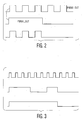
- Fig. 2 illustrates the basic timing waveforms for the dimmer control.
- the first waveform is the output of the individual PWM.
- the second waveform is the output of the group dimmer PWM.
- the third waveform is the resultant dimming waveform.
- the operation of the LED dimmer controller can be seen from an inspection of the waveforms shown in Fig. 2 . Due to the group dimmer signal, the resultant waveform has different ON and OFF times. This change in the average brightness of the LED is perceived by the human eye, which does an averaging operation, as dimming. It can be seen that by changing the value of the Pwm4_reg, the pulse width modulated output of the group PWM can be changed, which enables control of the resultant waveform, and hence provides for control of dimming the LED outputs.
- an LED dimmer controller in accordance with the invention must take into account factors such as, but not limited to, the following: the user interface operates at a different frequency (SCL clock domain) from the PWM frequency (OSC clock domain), hence there needs to be a clean handshake between these two clock domains; and the process of updating the LED outputs should be a smooth one rather than an abrupt one. The resulting update should happen so cleanly that the human eye does not perceive an abrupt switch.
- a method of updating all the LEDs together is provided by a mechanism referred to herein as "update on STOP".
- the actual update in the OSC clock domain is carefully controlled so that there are no visual artifacts resulting from the transfer of data across clock domain boundaries. This is achieved by a robust, synchronous, digital control mechanism.
- the illustrative PWM implementation is a counter/comparator implementation.
- a free running counter counts the number of clocks.
- a comparator compares the Pwm4_reg value with the counter to see if there is a match. If there is a match, then the Pwm4 output is asserted.
- a method for avoiding such visual artifacts includes determining that the Pwm4_reg in the SCL domain has been updated, and waiting for a STOP condition. Once the STOP condition occurs in the SCL clock domain, a clean clock boundary hand-shake across to the OSC clock domain is performed and a flag is set in the OSC clock domain. Subsequently, a wait state occurs until the Pwm4 counter in the OSC clock domain cleanly rolls over to zero. At this point in time, the Pwm4_reg shadow register in the OSC clock domain is updated to the new value. This procedure ensures that the new dim waveform is artifact-free.
- Fig. 3 illustrates the effect of following and not following the above-described procedure.
- various embodiments of the present invention include ensuring that the leading and trailing edges of the dimming waveform are separated in time from the original waveform.
- circuitry for this purpose. It will be further appreciated that careful attention is paid to the digital counter design and comparator design to ensure the edge separations described above are achieved.
- post-layout back annotated timing results should be analyzed to ensure that even after layout the above-described edge separations are valid.
- One advantage is that the visual artifacts, such as a flash of light during a dimming operation are eliminated.
- Another advantage is that synchronous digital designs in accordance with the present invention are verifiable through modern simulators and static timing analysis tools.
Landscapes
- Circuit Arrangement For Electric Light Sources In General (AREA)
- Led Devices (AREA)
Claims (13)
- Ein Verfahren zum Steuern eines LED basierten Beleuchtungsprodukts, welches eine Mehrzahl von LEDs hat, wobei das Verfahren aufweist:Erzeugen eines ersten Grundtaktes, wobei der erste Grundtakt eine erste Taktdomäne definiert;Erzeugen, innerhalb der ersten Taktdomäne, einer Mehrzahl von pulsbreitenmodulierten LED Steuersignalen, wobei jedes der Mehrzahl von pulsbreitenmodulierten LED Steuersignalen mit zumindest einer LED assoziiert ist;Erzeugen, innerhalb der ersten Taktdomäne, eines pulsbreitenmodulierten Gruppendimmersignals, undlogisches Kombinieren des Gruppendimmersignals mit jeder der Mehrzahl von pulsbreitenmodulierten LED Steuersignalen;wobei das Gruppendimmersignal erzeugt wird, so dass der kürzeste Puls des Gruppendimmersignals länger als der längste Puls irgendeines der Mehrzahl von pulsbreitenmodulierten LED Steuersignalen ist;wobei die Frequenz des Gruppendimmersignals bei einer geringeren Frequenz als die Frequenz des LED PWM Steuersignals liegt.
- Das Verfahren gemäß Anspruch 1, wobei Erzeugen jedes der Mehrzahl von pulsbreitenmodulierten LED Steuersignalen zumindest teilweise auf dem Inhalt eines Steuerregisters basiert, welches mit einem Pulsbreitenmodulator für jedes der Mehrzahl von pulsbreitenmodulierten LED Steuersignalen assoziiert ist.
- Das Verfahren gemäß Anspruch 2, wobei Erzeugen des Gruppendimmersignals zumindest teilweise auf dem Inhalt eines Steuerregisters basiert, welches mit einem Pulsbreitenmodulator für das Gruppendimmersignal assoziiert ist.
- Das Verfahren gemäß Anspruch 2, welches ferner aufweist, Empfangen, aus einer zweiten Taktdomäne, von aktualisiertem Inhalt für jedes Steuerregister, welches mit einem Pulsbreitenmodulator für jedes der Mehrzahl von pulsbreitenmodulierten LED Steuersignalen assoziiert ist.
- Das Verfahren gemäß Anspruch 2, welches ferner aufweist, Empfangen, aus einer zweiten Taktdomäne, von aktualisiertem Inhalt für das Steuerregister, welches mit einem Pulsbreitenmodulator für das Gruppendimmersignal assoziiert ist.
- Das Verfahren gemäß Anspruch 2, welches ferner aufweist, Empfangen, über einen I2C seriellen Bus, von aktualisiertem Inhalt für jedes Steuerregister, welches mit einem Pulsbreitenmodulator für jedes der Mehrzahl von pulsbreitenmodulierten LED Steuersignalen assoziiert ist, und von aktualisiertem Inhalt für das Steuerregister, welches mit einem Pulsbreitenmodulator für das Gruppendimmersignal assoziiert ist.
- Das Verfahren gemäß Anspruch 6, welches ferner aufweist, Bestimmen, dass eine I2C STOP Bedingung aufgetreten ist, vor einem Transferieren des aktualisierten Inhalts für jedes Steuerregister, welches mit dem Pulsbreitenmodulator für jedes der Mehrzahl von pulsbreitenmodulierten LED Steuersignalen assoziiert ist, und des aktualisierten Inhalts für das Steuerregister, welches mit dem Pulsbreitenmodulator für das Gruppendimmersignal assoziiert ist, zu der ersten Taktdomäne.
- Das Verfahren gemäß Anspruch 7, welches ferner aufweist, Setzen einer Flagge in der ersten Taktdomäne ansprechend auf das Bestimmen, dass eine I2C STOP Bedingung aufgetreten ist.
- Das Verfahren gemäß Anspruch 2, wobei die Mehrzahl der LEDs LEDs von verschiedenen Farben beinhaltet.
- Ein auf Puls Breiten Modulation basierender LED Dimmer, welcher aufweist:eine erste Oszillatorschaltung;einen ersten Zähler, der an die erste Oszillatorschaltung gekoppelt ist;eine Mehrzahl von individuellen Pulsbreitenmodulatorschaltungen, wobei jede der Mehrzahl von Pulsbreitenmodulatorschaltungen mit einer LED assoziiert ist, und jede an die erste Oszillatorschaltung und den ersten Zähler gekoppelt ist;eine Mehrzahl von Steuerregistern, wobei jedes der Mehrzahl von Steuerregistern mit zumindest einer der Mehrzahl von individuellen Pulsbreitenmodulatorschaltungen assoziiert ist;eine Gruppendimmer Pulsbreitenmodulatorschaltung und ein damit assoziiertes Steuerregister, wobei die Gruppendimmer Pulsbreitenmodulatorschaltung gekoppelt ist, um eine herunter geteilte Version eines Ausgangs des ersten Zählers zu empfangen; undkombinatorische Logik Gatter zum logischen Kombinieren von Ausgangssignalen der Mehrzahl von individuellen Pulsbreitenmodulatorschaltungen mit einem Ausgangssignal der Gruppendimmer Pulsbreitenmodulatorschaltung; wobeidie Pulsbreitenmodulatorschaltungen sich in einer ersten Taktdomäne befanden, die mittels der ersten Oszillatorschaltung definiert ist; und die Mehrzahl von Steuerregistern und das Steuerregister, welches mit dem Gruppendimmer assoziiert ist, eingerichtet sind, um Steuerinformation zu empfangen, die in einer zweiten Taktdomäne bei einer niedrigen Frequenz entspringt.
- Der auf Puls Breiten Modulation basierende LED Dimmer gemäß Anspruch 10, welcher ferner ein I2C serielles Businterface aufweist, das an die Steuerregister gekoppelt ist.
- Der auf Puls Breiten Modulation basierende LED Dimmer gemäß Anspruch 11, welcher ferner eine Flagge aufweist, die betriebsbereit ist, gesetzt zu werden, wenn eine I2C STOP Bedingung detektiert wird.
- Der auf Puls Breiten Modulation basierende LED Dimmer gemäß Anspruch 10, wobei die kombinatorischen Logik Gatter an LEDs gekoppelt sind.
Applications Claiming Priority (2)
| Application Number | Priority Date | Filing Date | Title |
|---|---|---|---|
| US78496306P | 2006-03-21 | 2006-03-21 | |
| PCT/IB2007/050977 WO2007107958A1 (en) | 2006-03-21 | 2007-03-20 | Pulse width modulation based led dimmer control |
Publications (2)
| Publication Number | Publication Date |
|---|---|
| EP2000007A1 EP2000007A1 (de) | 2008-12-10 |
| EP2000007B1 true EP2000007B1 (de) | 2012-06-27 |
Family
ID=38210553
Family Applications (1)
| Application Number | Title | Priority Date | Filing Date |
|---|---|---|---|
| EP07735197A Not-in-force EP2000007B1 (de) | 2006-03-21 | 2007-03-20 | Auf pulsbreitenmodulation basierende led-dimmersteuerung |
Country Status (6)
| Country | Link |
|---|---|
| US (1) | US7990081B2 (de) |
| EP (1) | EP2000007B1 (de) |
| JP (1) | JP2009530790A (de) |
| KR (1) | KR20090007341A (de) |
| CN (1) | CN101406107B (de) |
| WO (1) | WO2007107958A1 (de) |
Cited By (1)
| Publication number | Priority date | Publication date | Assignee | Title |
|---|---|---|---|---|
| US9419713B2 (en) | 2014-04-18 | 2016-08-16 | National Chiao Tung University | Visible light communication method |
Families Citing this family (32)
| Publication number | Priority date | Publication date | Assignee | Title |
|---|---|---|---|---|
| DE102008027148A1 (de) | 2008-06-03 | 2009-12-10 | Technisat Digital Gmbh | Verfahren zum Betrieb einer Lichtquelle eines Kraftfahrzeugs |
| US8232742B2 (en) | 2008-11-27 | 2012-07-31 | Arkalumen Inc. | Method, apparatus and computer-readable media for controlling lighting devices |
| CN102265324B (zh) | 2009-01-08 | 2014-12-24 | 杜比实验室特许公司 | 通用背光单元控制 |
| TWI387950B (zh) * | 2009-07-07 | 2013-03-01 | Holtek Semiconductor Inc | 一種電壓多重衰減控制裝置 |
| KR100975353B1 (ko) * | 2010-03-22 | 2010-08-11 | 제이엠씨엔지니어링 주식회사 | 발광 다이오드 회로 및 이를 포함하는 발광 다이오드 조명 장치 |
| US9089024B2 (en) | 2010-05-11 | 2015-07-21 | Arkalumen Inc. | Methods and apparatus for changing a DC supply voltage applied to a lighting circuit |
| US9086435B2 (en) | 2011-05-10 | 2015-07-21 | Arkalumen Inc. | Circuits for sensing current levels within a lighting apparatus incorporating a voltage converter |
| US8564214B2 (en) | 2010-05-11 | 2013-10-22 | Arkalumen Inc. | Circuits for sensing current levels within lighting apparatus |
| US8575841B2 (en) * | 2010-05-12 | 2013-11-05 | Kenall Manufacturing | MRI-room LED lighting system |
| US8646941B1 (en) | 2010-06-14 | 2014-02-11 | Humanscale Corporation | Lighting apparatus and method |
| KR101189253B1 (ko) * | 2010-11-10 | 2012-10-09 | 매그나칩 반도체 유한회사 | 고정위상 모드를 갖는 디지털 pwm방식에서 디밍 신호를 이용한 dc-dc 컨버터용 pwm 신호 생성회로 및 이를 이용한 led 구동회로 |
| US9192009B2 (en) | 2011-02-14 | 2015-11-17 | Arkalumen Inc. | Lighting apparatus and method for detecting reflected light from local objects |
| WO2012122638A1 (en) | 2011-03-16 | 2012-09-20 | Arkalumen Inc. | Lighting apparatus and methods for controlling lighting apparatus using ambient light levels |
| US8939604B2 (en) | 2011-03-25 | 2015-01-27 | Arkalumen Inc. | Modular LED strip lighting apparatus |
| US9060400B2 (en) | 2011-07-12 | 2015-06-16 | Arkalumen Inc. | Control apparatus incorporating a voltage converter for controlling lighting apparatus |
| US9013113B2 (en) | 2012-04-20 | 2015-04-21 | Apple Inc. | Keyboard backlight driver IC |
| US8981668B2 (en) * | 2013-03-08 | 2015-03-17 | LT Lighting (Taiwan) Corp. | Demand-side initiated dimmable LED lamp |
| US9775211B2 (en) | 2015-05-05 | 2017-09-26 | Arkalumen Inc. | Circuit and apparatus for controlling a constant current DC driver output |
| US9992829B2 (en) | 2015-05-05 | 2018-06-05 | Arkalumen Inc. | Control apparatus and system for coupling a lighting module to a constant current DC driver |
| US10568180B2 (en) | 2015-05-05 | 2020-02-18 | Arkalumen Inc. | Method and apparatus for controlling a lighting module having a plurality of LED groups |
| US10225904B2 (en) | 2015-05-05 | 2019-03-05 | Arkalumen, Inc. | Method and apparatus for controlling a lighting module based on a constant current level from a power source |
| US9992836B2 (en) | 2015-05-05 | 2018-06-05 | Arkawmen Inc. | Method, system and apparatus for activating a lighting module using a buffer load module |
| US10078055B2 (en) | 2015-05-19 | 2018-09-18 | AVID Labs, LLC | LED strobe |
| ITUB20151944A1 (it) * | 2015-07-07 | 2017-01-07 | Automotive Lighting Italia Spa | Metodo di regolazione dell’intensità luminosa e dispositivo di pilotaggio di sorgenti luminose |
| US9674911B2 (en) * | 2015-07-23 | 2017-06-06 | Dialog Semiconductor Inc. | Arbitrary pulse alignment to reduce LED flicker |
| CN105206228B (zh) * | 2015-10-16 | 2018-01-02 | 矽恩微电子(厦门)有限公司 | 亮度线性变化自行调节的led扫描阵列驱动芯片和调节方法 |
| US10624187B2 (en) | 2016-02-22 | 2020-04-14 | Energizer Brands, Llc | Light emitting diode driver regulated to consume constant battery current input |
| CN106102247B (zh) * | 2016-07-20 | 2018-09-04 | 杭州士兰微电子股份有限公司 | Led驱动装置及其控制方法 |
| JP7257654B2 (ja) * | 2018-09-12 | 2023-04-14 | 株式会社レイマック | 調光電源装置および撮像装置 |
| US11503683B2 (en) | 2020-07-31 | 2022-11-15 | Solum Co., Ltd. | Lighting device and controlling method thereof |
| US11523487B2 (en) | 2020-07-31 | 2022-12-06 | Solum Co., Ltd. | Lighting device and controlling method thereof |
| CN112954845A (zh) * | 2021-02-04 | 2021-06-11 | 上海晶丰明源半导体股份有限公司 | 一种led调光控制电路、方法、芯片及照明装置 |
Family Cites Families (8)
| Publication number | Priority date | Publication date | Assignee | Title |
|---|---|---|---|---|
| US6449289B1 (en) | 1998-10-09 | 2002-09-10 | Adaptec, Inc. | Multi-processor bus protocol system |
| US6621235B2 (en) * | 2001-08-03 | 2003-09-16 | Koninklijke Philips Electronics N.V. | Integrated LED driving device with current sharing for multiple LED strings |
| EP1445987A1 (de) * | 2003-02-04 | 2004-08-11 | Goodrich Hella Aerospace Lighting Systems GmbH | Vorrichtung zur Ansteuerung einer Leuchte mit Licht in mindestens zwei unterschiedlichen Farben aussendenden LED |
| JP4241487B2 (ja) * | 2004-04-20 | 2009-03-18 | ソニー株式会社 | Led駆動装置、バックライト光源装置及びカラー液晶表示装置 |
| US7633463B2 (en) * | 2004-04-30 | 2009-12-15 | Analog Devices, Inc. | Method and IC driver for series connected R, G, B LEDs |
| US7339323B2 (en) | 2005-04-29 | 2008-03-04 | 02Micro International Limited | Serial powering of an LED string |
| US7443104B2 (en) * | 2005-07-27 | 2008-10-28 | Osram Opto Semiconductors Gmbh | Lighting apparatus and method for controlling brightness and color location thereof |
| US7317403B2 (en) | 2005-08-26 | 2008-01-08 | Philips Lumileds Lighting Company, Llc | LED light source for backlighting with integrated electronics |
-
2007
- 2007-03-20 JP JP2009501006A patent/JP2009530790A/ja not_active Withdrawn
- 2007-03-20 US US12/294,001 patent/US7990081B2/en not_active Expired - Fee Related
- 2007-03-20 CN CN200780009927XA patent/CN101406107B/zh not_active Expired - Fee Related
- 2007-03-20 KR KR1020087025657A patent/KR20090007341A/ko not_active Ceased
- 2007-03-20 WO PCT/IB2007/050977 patent/WO2007107958A1/en not_active Ceased
- 2007-03-20 EP EP07735197A patent/EP2000007B1/de not_active Not-in-force
Cited By (1)
| Publication number | Priority date | Publication date | Assignee | Title |
|---|---|---|---|---|
| US9419713B2 (en) | 2014-04-18 | 2016-08-16 | National Chiao Tung University | Visible light communication method |
Also Published As
| Publication number | Publication date |
|---|---|
| KR20090007341A (ko) | 2009-01-16 |
| JP2009530790A (ja) | 2009-08-27 |
| US20090096392A1 (en) | 2009-04-16 |
| EP2000007A1 (de) | 2008-12-10 |
| CN101406107B (zh) | 2010-09-08 |
| US7990081B2 (en) | 2011-08-02 |
| WO2007107958A1 (en) | 2007-09-27 |
| CN101406107A (zh) | 2009-04-08 |
Similar Documents
| Publication | Publication Date | Title |
|---|---|---|
| US7990081B2 (en) | Pulse width modulation based LED dimmer control | |
| EP2042003B1 (de) | Vorrichtung und verfahren zur adressierung einer leistung an eine aus mehreren lasten ausgewählte last | |
| US10334672B2 (en) | Stochastic signal density modulation for optical transducer control | |
| US7915838B2 (en) | Delta-sigma signal density modulation for optical transducer control | |
| US20120207205A1 (en) | Phase-shifted pulse width modulation signal generation device and method therefor | |
| CN102771189B (zh) | 检测器电路和用于操作检测器电路的方法 | |
| US11134554B2 (en) | Control method for combined lamp, and illumination system | |
| JP2016027575A (ja) | 統合ledディマコントローラ | |
| CN105206228A (zh) | 亮度线性变化自行调节的led扫描阵列驱动芯片和调节方法 | |
| CN112954845A (zh) | 一种led调光控制电路、方法、芯片及照明装置 | |
| US10674578B1 (en) | Pipelined exponential law brightness conversion for a multi-channel LED driver | |
| US11134553B2 (en) | Lighting memory device and memory module | |
| CN107480090A (zh) | 一种在串行外设接口设备上实现gpio功能的电路及方法 | |
| CN107454703A (zh) | 发光装置及其控制方法 | |
| CN216391471U (zh) | 调节信号占空比的电路及led灯具 | |
| CN104049930B (zh) | 亮度调节电路 | |
| JP7515014B2 (ja) | Led照明装置の駆動用装置、led照明装置、及びled照明装置の駆動用装置の製造方法 | |
| CN107908269A (zh) | 一种多pol并联组合供电系统及供电方法 | |
| EP4586101A1 (de) | Gemeinsame leiter für bidirektionale signale | |
| CN217159734U (zh) | 网络状态指示电路 | |
| CN210348473U (zh) | 一种网口显示电路和服务器 | |
| WO2019037250A1 (zh) | 一种调光调色灯丝灯 | |
| CN107221285A (zh) | 一种电子显示电路 | |
| CN119997293A (zh) | 一种驱动led通道的控制电路、方法、系统 | |
| WO2025151220A1 (en) | Shared conductor for signals differing in frequency |
Legal Events
| Date | Code | Title | Description |
|---|---|---|---|
| PUAI | Public reference made under article 153(3) epc to a published international application that has entered the european phase |
Free format text: ORIGINAL CODE: 0009012 |
|
| 17P | Request for examination filed |
Effective date: 20081021 |
|
| AK | Designated contracting states |
Kind code of ref document: A1 Designated state(s): AT BE BG CH CY CZ DE DK EE ES FI FR GB GR HU IE IS IT LI LT LU LV MC MT NL PL PT RO SE SI SK TR |
|
| 17Q | First examination report despatched |
Effective date: 20090203 |
|
| GRAP | Despatch of communication of intention to grant a patent |
Free format text: ORIGINAL CODE: EPIDOSNIGR1 |
|
| DAX | Request for extension of the european patent (deleted) | ||
| GRAS | Grant fee paid |
Free format text: ORIGINAL CODE: EPIDOSNIGR3 |
|
| GRAA | (expected) grant |
Free format text: ORIGINAL CODE: 0009210 |
|
| AK | Designated contracting states |
Kind code of ref document: B1 Designated state(s): AT BE BG CH CY CZ DE DK EE ES FI FR GB GR HU IE IS IT LI LT LU LV MC MT NL PL PT RO SE SI SK TR |
|
| REG | Reference to a national code |
Ref country code: GB Ref legal event code: FG4D |
|
| REG | Reference to a national code |
Ref country code: CH Ref legal event code: EP |
|
| REG | Reference to a national code |
Ref country code: AT Ref legal event code: REF Ref document number: 564734 Country of ref document: AT Kind code of ref document: T Effective date: 20120715 |
|
| REG | Reference to a national code |
Ref country code: IE Ref legal event code: FG4D |
|
| REG | Reference to a national code |
Ref country code: DE Ref legal event code: R096 Ref document number: 602007023612 Country of ref document: DE Effective date: 20120823 |
|
| PG25 | Lapsed in a contracting state [announced via postgrant information from national office to epo] |
Ref country code: SE Free format text: LAPSE BECAUSE OF FAILURE TO SUBMIT A TRANSLATION OF THE DESCRIPTION OR TO PAY THE FEE WITHIN THE PRESCRIBED TIME-LIMIT Effective date: 20120627 Ref country code: LT Free format text: LAPSE BECAUSE OF FAILURE TO SUBMIT A TRANSLATION OF THE DESCRIPTION OR TO PAY THE FEE WITHIN THE PRESCRIBED TIME-LIMIT Effective date: 20120627 Ref country code: FI Free format text: LAPSE BECAUSE OF FAILURE TO SUBMIT A TRANSLATION OF THE DESCRIPTION OR TO PAY THE FEE WITHIN THE PRESCRIBED TIME-LIMIT Effective date: 20120627 |
|
| REG | Reference to a national code |
Ref country code: NL Ref legal event code: VDEP Effective date: 20120627 |
|
| REG | Reference to a national code |
Ref country code: AT Ref legal event code: MK05 Ref document number: 564734 Country of ref document: AT Kind code of ref document: T Effective date: 20120627 |
|
| REG | Reference to a national code |
Ref country code: LT Ref legal event code: MG4D Effective date: 20120627 |
|
| PG25 | Lapsed in a contracting state [announced via postgrant information from national office to epo] |
Ref country code: LV Free format text: LAPSE BECAUSE OF FAILURE TO SUBMIT A TRANSLATION OF THE DESCRIPTION OR TO PAY THE FEE WITHIN THE PRESCRIBED TIME-LIMIT Effective date: 20120627 Ref country code: SI Free format text: LAPSE BECAUSE OF FAILURE TO SUBMIT A TRANSLATION OF THE DESCRIPTION OR TO PAY THE FEE WITHIN THE PRESCRIBED TIME-LIMIT Effective date: 20120627 Ref country code: GR Free format text: LAPSE BECAUSE OF FAILURE TO SUBMIT A TRANSLATION OF THE DESCRIPTION OR TO PAY THE FEE WITHIN THE PRESCRIBED TIME-LIMIT Effective date: 20120928 |
|
| PG25 | Lapsed in a contracting state [announced via postgrant information from national office to epo] |
Ref country code: RO Free format text: LAPSE BECAUSE OF FAILURE TO SUBMIT A TRANSLATION OF THE DESCRIPTION OR TO PAY THE FEE WITHIN THE PRESCRIBED TIME-LIMIT Effective date: 20120627 Ref country code: IS Free format text: LAPSE BECAUSE OF FAILURE TO SUBMIT A TRANSLATION OF THE DESCRIPTION OR TO PAY THE FEE WITHIN THE PRESCRIBED TIME-LIMIT Effective date: 20121027 Ref country code: AT Free format text: LAPSE BECAUSE OF FAILURE TO SUBMIT A TRANSLATION OF THE DESCRIPTION OR TO PAY THE FEE WITHIN THE PRESCRIBED TIME-LIMIT Effective date: 20120627 Ref country code: EE Free format text: LAPSE BECAUSE OF FAILURE TO SUBMIT A TRANSLATION OF THE DESCRIPTION OR TO PAY THE FEE WITHIN THE PRESCRIBED TIME-LIMIT Effective date: 20120627 Ref country code: SK Free format text: LAPSE BECAUSE OF FAILURE TO SUBMIT A TRANSLATION OF THE DESCRIPTION OR TO PAY THE FEE WITHIN THE PRESCRIBED TIME-LIMIT Effective date: 20120627 Ref country code: BE Free format text: LAPSE BECAUSE OF FAILURE TO SUBMIT A TRANSLATION OF THE DESCRIPTION OR TO PAY THE FEE WITHIN THE PRESCRIBED TIME-LIMIT Effective date: 20120627 Ref country code: CZ Free format text: LAPSE BECAUSE OF FAILURE TO SUBMIT A TRANSLATION OF THE DESCRIPTION OR TO PAY THE FEE WITHIN THE PRESCRIBED TIME-LIMIT Effective date: 20120627 Ref country code: CY Free format text: LAPSE BECAUSE OF FAILURE TO SUBMIT A TRANSLATION OF THE DESCRIPTION OR TO PAY THE FEE WITHIN THE PRESCRIBED TIME-LIMIT Effective date: 20120627 |
|
| PG25 | Lapsed in a contracting state [announced via postgrant information from national office to epo] |
Ref country code: IT Free format text: LAPSE BECAUSE OF FAILURE TO SUBMIT A TRANSLATION OF THE DESCRIPTION OR TO PAY THE FEE WITHIN THE PRESCRIBED TIME-LIMIT Effective date: 20120627 Ref country code: PL Free format text: LAPSE BECAUSE OF FAILURE TO SUBMIT A TRANSLATION OF THE DESCRIPTION OR TO PAY THE FEE WITHIN THE PRESCRIBED TIME-LIMIT Effective date: 20120627 Ref country code: PT Free format text: LAPSE BECAUSE OF FAILURE TO SUBMIT A TRANSLATION OF THE DESCRIPTION OR TO PAY THE FEE WITHIN THE PRESCRIBED TIME-LIMIT Effective date: 20121029 |
|
| PG25 | Lapsed in a contracting state [announced via postgrant information from national office to epo] |
Ref country code: NL Free format text: LAPSE BECAUSE OF FAILURE TO SUBMIT A TRANSLATION OF THE DESCRIPTION OR TO PAY THE FEE WITHIN THE PRESCRIBED TIME-LIMIT Effective date: 20120627 |
|
| PG25 | Lapsed in a contracting state [announced via postgrant information from national office to epo] |
Ref country code: ES Free format text: LAPSE BECAUSE OF FAILURE TO SUBMIT A TRANSLATION OF THE DESCRIPTION OR TO PAY THE FEE WITHIN THE PRESCRIBED TIME-LIMIT Effective date: 20121008 Ref country code: DK Free format text: LAPSE BECAUSE OF FAILURE TO SUBMIT A TRANSLATION OF THE DESCRIPTION OR TO PAY THE FEE WITHIN THE PRESCRIBED TIME-LIMIT Effective date: 20120627 |
|
| PLBE | No opposition filed within time limit |
Free format text: ORIGINAL CODE: 0009261 |
|
| STAA | Information on the status of an ep patent application or granted ep patent |
Free format text: STATUS: NO OPPOSITION FILED WITHIN TIME LIMIT |
|
| 26N | No opposition filed |
Effective date: 20130328 |
|
| REG | Reference to a national code |
Ref country code: DE Ref legal event code: R097 Ref document number: 602007023612 Country of ref document: DE Effective date: 20130328 |
|
| PG25 | Lapsed in a contracting state [announced via postgrant information from national office to epo] |
Ref country code: BG Free format text: LAPSE BECAUSE OF FAILURE TO SUBMIT A TRANSLATION OF THE DESCRIPTION OR TO PAY THE FEE WITHIN THE PRESCRIBED TIME-LIMIT Effective date: 20120927 |
|
| PG25 | Lapsed in a contracting state [announced via postgrant information from national office to epo] |
Ref country code: MC Free format text: LAPSE BECAUSE OF NON-PAYMENT OF DUE FEES Effective date: 20130331 |
|
| REG | Reference to a national code |
Ref country code: CH Ref legal event code: PL |
|
| REG | Reference to a national code |
Ref country code: IE Ref legal event code: MM4A |
|
| PG25 | Lapsed in a contracting state [announced via postgrant information from national office to epo] |
Ref country code: LI Free format text: LAPSE BECAUSE OF NON-PAYMENT OF DUE FEES Effective date: 20130331 Ref country code: IE Free format text: LAPSE BECAUSE OF NON-PAYMENT OF DUE FEES Effective date: 20130320 Ref country code: CH Free format text: LAPSE BECAUSE OF NON-PAYMENT OF DUE FEES Effective date: 20130331 |
|
| PG25 | Lapsed in a contracting state [announced via postgrant information from national office to epo] |
Ref country code: MT Free format text: LAPSE BECAUSE OF FAILURE TO SUBMIT A TRANSLATION OF THE DESCRIPTION OR TO PAY THE FEE WITHIN THE PRESCRIBED TIME-LIMIT Effective date: 20120627 |
|
| PG25 | Lapsed in a contracting state [announced via postgrant information from national office to epo] |
Ref country code: TR Free format text: LAPSE BECAUSE OF FAILURE TO SUBMIT A TRANSLATION OF THE DESCRIPTION OR TO PAY THE FEE WITHIN THE PRESCRIBED TIME-LIMIT Effective date: 20120627 |
|
| PG25 | Lapsed in a contracting state [announced via postgrant information from national office to epo] |
Ref country code: HU Free format text: LAPSE BECAUSE OF FAILURE TO SUBMIT A TRANSLATION OF THE DESCRIPTION OR TO PAY THE FEE WITHIN THE PRESCRIBED TIME-LIMIT; INVALID AB INITIO Effective date: 20070320 Ref country code: LU Free format text: LAPSE BECAUSE OF NON-PAYMENT OF DUE FEES Effective date: 20130320 |
|
| REG | Reference to a national code |
Ref country code: FR Ref legal event code: PLFP Year of fee payment: 10 |
|
| REG | Reference to a national code |
Ref country code: FR Ref legal event code: PLFP Year of fee payment: 11 |
|
| REG | Reference to a national code |
Ref country code: FR Ref legal event code: PLFP Year of fee payment: 12 |
|
| REG | Reference to a national code |
Ref country code: DE Ref legal event code: R079 Ref document number: 602007023612 Country of ref document: DE Free format text: PREVIOUS MAIN CLASS: H05B0033080000 Ipc: H05B0045000000 |
|
| PGFP | Annual fee paid to national office [announced via postgrant information from national office to epo] |
Ref country code: GB Payment date: 20220225 Year of fee payment: 16 Ref country code: DE Payment date: 20220217 Year of fee payment: 16 |
|
| PGFP | Annual fee paid to national office [announced via postgrant information from national office to epo] |
Ref country code: FR Payment date: 20220221 Year of fee payment: 16 |
|
| REG | Reference to a national code |
Ref country code: DE Ref legal event code: R119 Ref document number: 602007023612 Country of ref document: DE |
|
| GBPC | Gb: european patent ceased through non-payment of renewal fee |
Effective date: 20230320 |
|
| PG25 | Lapsed in a contracting state [announced via postgrant information from national office to epo] |
Ref country code: GB Free format text: LAPSE BECAUSE OF NON-PAYMENT OF DUE FEES Effective date: 20230320 |
|
| PG25 | Lapsed in a contracting state [announced via postgrant information from national office to epo] |
Ref country code: GB Free format text: LAPSE BECAUSE OF NON-PAYMENT OF DUE FEES Effective date: 20230320 Ref country code: FR Free format text: LAPSE BECAUSE OF NON-PAYMENT OF DUE FEES Effective date: 20230331 Ref country code: DE Free format text: LAPSE BECAUSE OF NON-PAYMENT OF DUE FEES Effective date: 20231003 |