EP1997111B1 - Speichervorrichtung mit modus-auswählbarer vorausladung und clock-to-core-taktung - Google Patents
Speichervorrichtung mit modus-auswählbarer vorausladung und clock-to-core-taktung Download PDFInfo
- Publication number
- EP1997111B1 EP1997111B1 EP07758147A EP07758147A EP1997111B1 EP 1997111 B1 EP1997111 B1 EP 1997111B1 EP 07758147 A EP07758147 A EP 07758147A EP 07758147 A EP07758147 A EP 07758147A EP 1997111 B1 EP1997111 B1 EP 1997111B1
- Authority
- EP
- European Patent Office
- Prior art keywords
- data
- prefetch
- memory
- memory device
- mode
- Prior art date
- Legal status (The legal status is an assumption and is not a legal conclusion. Google has not performed a legal analysis and makes no representation as to the accuracy of the status listed.)
- Revoked
Links
- 239000000872 buffer Substances 0.000 claims abstract description 93
- 230000011664 signaling Effects 0.000 claims abstract description 30
- 230000015654 memory Effects 0.000 claims description 147
- 230000004044 response Effects 0.000 claims description 30
- 210000000352 storage cell Anatomy 0.000 claims description 12
- 238000000034 method Methods 0.000 claims description 6
- 238000012546 transfer Methods 0.000 abstract description 34
- 239000012536 storage buffer Substances 0.000 abstract description 3
- 230000005540 biological transmission Effects 0.000 description 48
- 230000004913 activation Effects 0.000 description 15
- 238000012545 processing Methods 0.000 description 7
- 239000004020 conductor Substances 0.000 description 6
- 230000007704 transition Effects 0.000 description 5
- 238000009432 framing Methods 0.000 description 4
- 230000000873 masking effect Effects 0.000 description 4
- 230000008901 benefit Effects 0.000 description 3
- 238000013500 data storage Methods 0.000 description 3
- 238000013461 design Methods 0.000 description 3
- 230000003287 optical effect Effects 0.000 description 3
- 239000004065 semiconductor Substances 0.000 description 3
- 230000001360 synchronised effect Effects 0.000 description 3
- 230000003542 behavioural effect Effects 0.000 description 2
- 230000002457 bidirectional effect Effects 0.000 description 2
- 239000000470 constituent Substances 0.000 description 2
- 238000010586 diagram Methods 0.000 description 2
- 238000005516 engineering process Methods 0.000 description 2
- 230000014509 gene expression Effects 0.000 description 2
- 238000004519 manufacturing process Methods 0.000 description 2
- 238000011084 recovery Methods 0.000 description 2
- 230000000630 rising effect Effects 0.000 description 2
- 238000005070 sampling Methods 0.000 description 2
- 230000003068 static effect Effects 0.000 description 2
- 238000003491 array Methods 0.000 description 1
- 230000008859 change Effects 0.000 description 1
- 238000004590 computer program Methods 0.000 description 1
- 238000011960 computer-aided design Methods 0.000 description 1
- 238000013481 data capture Methods 0.000 description 1
- 230000001419 dependent effect Effects 0.000 description 1
- 238000007667 floating Methods 0.000 description 1
- 230000006870 function Effects 0.000 description 1
- 230000006872 improvement Effects 0.000 description 1
- 229910044991 metal oxide Inorganic materials 0.000 description 1
- 150000004706 metal oxides Chemical class 0.000 description 1
- 230000008520 organization Effects 0.000 description 1
- 230000008569 process Effects 0.000 description 1
- 238000012358 sourcing Methods 0.000 description 1
- 230000001960 triggered effect Effects 0.000 description 1
Images


Classifications
-
- G—PHYSICS
- G11—INFORMATION STORAGE
- G11C—STATIC STORES
- G11C11/00—Digital stores characterised by the use of particular electric or magnetic storage elements; Storage elements therefor
- G11C11/21—Digital stores characterised by the use of particular electric or magnetic storage elements; Storage elements therefor using electric elements
- G11C11/34—Digital stores characterised by the use of particular electric or magnetic storage elements; Storage elements therefor using electric elements using semiconductor devices
- G11C11/40—Digital stores characterised by the use of particular electric or magnetic storage elements; Storage elements therefor using electric elements using semiconductor devices using transistors
- G11C11/401—Digital stores characterised by the use of particular electric or magnetic storage elements; Storage elements therefor using electric elements using semiconductor devices using transistors forming cells needing refreshing or charge regeneration, i.e. dynamic cells
- G11C11/4063—Auxiliary circuits, e.g. for addressing, decoding, driving, writing, sensing or timing
- G11C11/407—Auxiliary circuits, e.g. for addressing, decoding, driving, writing, sensing or timing for memory cells of the field-effect type
- G11C11/409—Read-write [R-W] circuits
- G11C11/4093—Input/output [I/O] data interface arrangements, e.g. data buffers
-
- G—PHYSICS
- G11—INFORMATION STORAGE
- G11C—STATIC STORES
- G11C7/00—Arrangements for writing information into, or reading information out from, a digital store
- G11C7/10—Input/output [I/O] data interface arrangements, e.g. I/O data control circuits, I/O data buffers
- G11C7/1015—Read-write modes for single port memories, i.e. having either a random port or a serial port
- G11C7/1039—Read-write modes for single port memories, i.e. having either a random port or a serial port using pipelining techniques, i.e. using latches between functional memory parts, e.g. row/column decoders, I/O buffers, sense amplifiers
-
- G—PHYSICS
- G11—INFORMATION STORAGE
- G11C—STATIC STORES
- G11C11/00—Digital stores characterised by the use of particular electric or magnetic storage elements; Storage elements therefor
- G11C11/21—Digital stores characterised by the use of particular electric or magnetic storage elements; Storage elements therefor using electric elements
- G11C11/34—Digital stores characterised by the use of particular electric or magnetic storage elements; Storage elements therefor using electric elements using semiconductor devices
- G11C11/40—Digital stores characterised by the use of particular electric or magnetic storage elements; Storage elements therefor using electric elements using semiconductor devices using transistors
- G11C11/401—Digital stores characterised by the use of particular electric or magnetic storage elements; Storage elements therefor using electric elements using semiconductor devices using transistors forming cells needing refreshing or charge regeneration, i.e. dynamic cells
- G11C11/4063—Auxiliary circuits, e.g. for addressing, decoding, driving, writing, sensing or timing
- G11C11/407—Auxiliary circuits, e.g. for addressing, decoding, driving, writing, sensing or timing for memory cells of the field-effect type
- G11C11/4076—Timing circuits
-
- G—PHYSICS
- G11—INFORMATION STORAGE
- G11C—STATIC STORES
- G11C11/00—Digital stores characterised by the use of particular electric or magnetic storage elements; Storage elements therefor
- G11C11/21—Digital stores characterised by the use of particular electric or magnetic storage elements; Storage elements therefor using electric elements
- G11C11/34—Digital stores characterised by the use of particular electric or magnetic storage elements; Storage elements therefor using electric elements using semiconductor devices
- G11C11/40—Digital stores characterised by the use of particular electric or magnetic storage elements; Storage elements therefor using electric elements using semiconductor devices using transistors
- G11C11/401—Digital stores characterised by the use of particular electric or magnetic storage elements; Storage elements therefor using electric elements using semiconductor devices using transistors forming cells needing refreshing or charge regeneration, i.e. dynamic cells
- G11C11/4063—Auxiliary circuits, e.g. for addressing, decoding, driving, writing, sensing or timing
- G11C11/407—Auxiliary circuits, e.g. for addressing, decoding, driving, writing, sensing or timing for memory cells of the field-effect type
- G11C11/408—Address circuits
-
- G—PHYSICS
- G11—INFORMATION STORAGE
- G11C—STATIC STORES
- G11C11/00—Digital stores characterised by the use of particular electric or magnetic storage elements; Storage elements therefor
- G11C11/21—Digital stores characterised by the use of particular electric or magnetic storage elements; Storage elements therefor using electric elements
- G11C11/34—Digital stores characterised by the use of particular electric or magnetic storage elements; Storage elements therefor using electric elements using semiconductor devices
- G11C11/40—Digital stores characterised by the use of particular electric or magnetic storage elements; Storage elements therefor using electric elements using semiconductor devices using transistors
- G11C11/401—Digital stores characterised by the use of particular electric or magnetic storage elements; Storage elements therefor using electric elements using semiconductor devices using transistors forming cells needing refreshing or charge regeneration, i.e. dynamic cells
- G11C11/4063—Auxiliary circuits, e.g. for addressing, decoding, driving, writing, sensing or timing
- G11C11/407—Auxiliary circuits, e.g. for addressing, decoding, driving, writing, sensing or timing for memory cells of the field-effect type
- G11C11/409—Read-write [R-W] circuits
- G11C11/4096—Input/output [I/O] data management or control circuits, e.g. reading or writing circuits, I/O drivers or bit-line switches
-
- G—PHYSICS
- G11—INFORMATION STORAGE
- G11C—STATIC STORES
- G11C7/00—Arrangements for writing information into, or reading information out from, a digital store
- G11C7/10—Input/output [I/O] data interface arrangements, e.g. I/O data control circuits, I/O data buffers
- G11C7/1006—Data managing, e.g. manipulating data before writing or reading out, data bus switches or control circuits therefor
- G11C7/1012—Data reordering during input/output, e.g. crossbars, layers of multiplexers, shifting or rotating
-
- G—PHYSICS
- G11—INFORMATION STORAGE
- G11C—STATIC STORES
- G11C7/00—Arrangements for writing information into, or reading information out from, a digital store
- G11C7/10—Input/output [I/O] data interface arrangements, e.g. I/O data control circuits, I/O data buffers
- G11C7/1015—Read-write modes for single port memories, i.e. having either a random port or a serial port
- G11C7/1042—Read-write modes for single port memories, i.e. having either a random port or a serial port using interleaving techniques, i.e. read-write of one part of the memory while preparing another part
-
- G—PHYSICS
- G11—INFORMATION STORAGE
- G11C—STATIC STORES
- G11C7/00—Arrangements for writing information into, or reading information out from, a digital store
- G11C7/10—Input/output [I/O] data interface arrangements, e.g. I/O data control circuits, I/O data buffers
- G11C7/1051—Data output circuits, e.g. read-out amplifiers, data output buffers, data output registers, data output level conversion circuits
- G11C7/1066—Output synchronization
-
- G—PHYSICS
- G11—INFORMATION STORAGE
- G11C—STATIC STORES
- G11C7/00—Arrangements for writing information into, or reading information out from, a digital store
- G11C7/22—Read-write [R-W] timing or clocking circuits; Read-write [R-W] control signal generators or management
-
- G—PHYSICS
- G11—INFORMATION STORAGE
- G11C—STATIC STORES
- G11C2207/00—Indexing scheme relating to arrangements for writing information into, or reading information out from, a digital store
- G11C2207/10—Aspects relating to interfaces of memory device to external buses
- G11C2207/107—Serial-parallel conversion of data or prefetch
Definitions
- the present invention relates to integrated circuits, data processing and data storage within a data processing system.
- DRAMs dynamic random access memories
- DRAM architectures that output only a selected portion of prefetched data have been proposed, such architectures generally prefetch an amount of data that corresponds to the maximum prefetch size, completely filling a data buffer in the prefetch operation, then outputting only a portion of the buffered data. Consequently, a substantial quantity of non-requested data may be retrieved from the core and stored in the data buffer of such selectable-output-size devices, thus needlessly consuming power and increasing thermal loading.
- the US 51778,436 discloses a memory device ( fig.3 ) wherein a read data buffer (40) is loaded with data from a storage array (70) via a number of data lines which corresponds to the number of columns of the storage array.
- a read data buffer 40
- a storage array 70
- predictive cache memory systems and methods which are responsive to cache misses to prefetch a data block from main memory based upon the data block which last followed the memory address which caused the cache miss.
- a second main memory data block is identified which was accessed following a previous access request to the main memory for the first main memory data block.
- the second memory data block is stored in a predictive cache if the second main memory data block is not already stored in the predictive cache.
- the identification of data blocks for prefetching may be provided by a prediction table which stores therein identifications of a plurality of succeeding main memory data blocks, each of which was accessed following an access request to a corresponding one of a plurality of preceding main memory data blocks.
- the Prediction Table is updated if predictions are incorrect.
- the predictive cache may be implemented using on-chip SRAM cache which is integrated with a DRAM array so that transfers between the DRAM array and the predictive cache may occur at high speed using an internal buffer.
- the US 5,329,489 discloses a memory device ( fig.4 ) wherein a read data buffer (72) is loaded with data from a storage array (71) via number of data lines which corresponds to a subset of the number of columns of the storage array.
- a random access array memory device which uses a static buffer as a cache for speeding the access times achievable for data retrieval from the device.
- the static buffer is operationally divided into two or more blocks so that each block holds a block of data from a different row of the array. The division of a single buffer into several operational blocks significantly increases the "hit" probability of the cache, allowing fast access from the buffer.
- a control system stores the row address (TAG) of each of the multiple blocks and compares that address to the row address of the data desired and signals the result of that comparison.
- Random access memory arrays of the multiple line cache configuration are employed in data processing systems including a CPU, address and data buses, control logic, and multiplexers.
- the prefetch modes include a full prefetch mode in which an amount of data that corresponds to a maximum prefetch size is retrieved from the memory core and stored in a read data buffer before being transmitted, and one or more partial prefetch modes in which an amount of data that corresponds to a fraction of the maximum prefetch size is retrieved from the memory core and stored in the read data buffer before transmission.
- a reduced amount of data is transferred from the memory core to the read data buffer in a partial prefetch mode (i.e., as compared to the full amount data transferred in the full prefetch mode)
- selected signal lines within the internal data path between the memory core and the read data buffer need not be driven and selected storage elements within the read data buffer need not be loaded. Accordingly, by driving only that subset of the signal lines within the internal data path needed to convey the reduced amount of prefetch data, and/or by loading only the subset of storage elements within the read data buffer needed to store the reduced amount of prefetch data, substantial power savings may be realized. Further power may be saved during write operations by driving only a subset of the signal lines of the internal data path with write data.
- the relative timing between a clock signal used to time data transmit and/or receive operations (or otherwise control operations within the memory device) and the minimum time between successive accesses to the same storage resource within the memory core may be specified by a configuration register value, thus establishing a corresponding determination of the number of memory core resources that may be accessed in each core cycle time. For example, in one embodiment, if the configuration register value specifies more than a threshold number of clock cycles per core cycle time, the memory device operates in a mode in which two or more resources within the memory core are independently addressed and accessed during each core cycle time to ensure that sufficient data is retrieved from (or written to the core) to keep pace with the peak signaling bandwidth afforded by the clock rate.
- the memory device operates in a mode in which a single core access is performed during each core cycle time.
- an internal configuration register may be run-time or production-time programmed to establish the desired settings.
- input signals that are, for example, strapped to supply or ground reference voltages or supplied by a control device, may be used to control the prefetch data size and/or to specify the clock-to-core ratio.
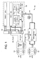
- Figure 1 illustrates an embodiment of a memory device 100 having circuitry to support scaled prefetch modes, including a full prefetch mode and at least one partial prefetch mode.
- the memory device 100 is a dynamic random access memory (DRAM) device that includes, among its component circuit blocks, a data interface 101, request interface 103, request logic 105, read and write data pipes 109 and 111, row and column decoders 113 and 115, and memory core 125.
- DRAM dynamic random access memory
- the memory device 100 may be any other type of memory device that may benefit from scaled prefetch operation.
- the request interface 103 is coupled to receive memory access requests and configuration requests from a memory controller or other control device via external request path 104, and the data interface 101 is coupled to receive write data from the memory controller and transmit read data to the memory controller via external data path 102.
- the request interface 103 is a unidirectional synchronous interface that includes a bank of sampling circuits to sample incoming request signals in response to one or more timing signals (e.g., clock signals or strobe signals conveyed on separate signal lines or recovered from the data or request signals using clock-data recovery techniques), thereby recovering multi-bit requests that are passed to the request logic 105.
- timing signals e.g., clock signals or strobe signals conveyed on separate signal lines or recovered from the data or request signals using clock-data recovery techniques
- the data interface 101 is a bidirectional synchronous interface having sampling circuits to sample incoming write data signals (or other information) in response to one or more timing signals as well as output driver circuits to transmit read data signals in response to a transmit clock signal or strobe signal.
- separate unidirectional interfaces may be provided for receipt of write data and transmission of read data, and/or the request interface 103 may be bidirectional, for example, to enable requests to be acknowledged or to allow the memory device 100 to initiate requests to the memory controller.
- request signals and/or data signals may be conveyed between the memory controller and memory device 100 asynchronously in alternative embodiments.
- the external signal paths 102, 104 may each be implemented by single-ended or differential point-to-point signaling links and/or multi-drop signaling links.
- each incoming request is received in a sequence of transfers over the request path 104, with the individual time slices of the request being accumulated within the request logic 105 until the entire request is received (alternatively, if the request path is wide enough, all the bits of a request may be received in a single transfer over the request path) and includes an operation code which indicates the nature of the requested operation (e.g., row activation, column read, column write, precharge, register write, refresh, etc.) and, in the case of a memory access request, one or more address values that specify the row and/or column to be accessed within the memory core 125.
- the one or more addresses or any of them may be conveyed in time-multiplexed fashion over the external data path 102 or via a dedicated address signal path.
- the request logic 105 decodes the incoming requests and issues control and timing signals to other circuit blocks within the memory device 100 to carry out the requested operation, including issuing row address, bank address and control information (RA, BA, Ctl) to the row decoder 113 in response to a row activation request, and column address, bank address and control information (CA, BA, Ctl) to the column decoder 115 and load control information to the read data pipe 109 and write data pipe 111 in response to column access requests.
- the information provided to the decoders 113, 115 and data pipes 109, 111 may indicate one of a number of different prefetch modes, including the full prefetch mode and partial prefetch mode discussed above.
- the request logic 105 may include one or more configuration circuits 107 implemented, for example, by a programmable configuration register or other volatile circuitry, or by non-volatile circuitry such as a one-time-programmable elements (e.g., fuse-controlled logic), floating-gate devices or any other nonvolatile storage).
- configuration circuits 107 implemented, for example, by a programmable configuration register or other volatile circuitry, or by non-volatile circuitry such as a one-time-programmable elements (e.g., fuse-controlled logic), floating-gate devices or any other nonvolatile storage).
- the prefetch mode of the memory device 100 is controlled through programming (i.e., storing in response to a host instruction) a prefetch mode value in the configuration circuit 107, thus effecting a selection of one of multiple possible prefetch modes, including a full prefetch mode and one or more partial prefetch modes.
- the configuration circuit may be separate from the request logic 105 in alternative embodiments.
- the prefetch mode may be controlled via the state of signals received via the request interface 103, data interface 101 or another interface.
- a set of prefetch signal inputs (or at least one signal input) is provided to receive a prefetch mode signal that is used to control the prefetch mode with in the memory device 100.
- the prefetch signal inputs may be strapped to logic levels (e.g., tied high and/or low by interconnections between the memory device 100 and circuit-board or chip-package ground and supply voltage lines) or may be received from another integrated circuit device.
- the memory core 125 includes a storage array formed by multiple (K) independently addressable banks of storage cells, 131 0 -131 K-1 , each of which includes multiple (J) subbanks 135 0 -135 J-1 .
- Each of the subbanks 135 includes storage cells arranged in rows 152 and columns 154, with word lines 134 coupled to each row of storage cells and bit lines (not shown) coupled to each column of storage cells.
- Each subbank 135 additionally includes a set of sense amplifiers (not shown in Figure 1 ) coupled to the bit lines, the set of sense amplifiers for each bank (131) of storage cells constituting a sense amplifier bank. Note that the sense amplifiers may be viewed as an entity separate from the subbanks 135, banks 131 or memory core 125.
- the request logic 105 provides a bank address (BA) and row address (RA), received with or in association with the request, to the row decoder 113 and asserts a decode-enable signal (i.e., part of the control information, Ctl) to enable a row decoding operation therein.
- the row decoder 113 responds to the decode-enable signal by decoding the bank address to select one of the K banks (131) of storage cells for row activation, and decoding the row address to activate the row-address-specified one of the word lines 134 within the selected bank 131.
- Word line activation enables the contents of the corresponding row of storage cells (i.e., the storage cells coupled to the activated word line) to drive the bit lines within each of the subbanks 135 of the address-selected bank 131. Simultaneously with word line activation, or after a period of time sufficient to enable the stored data to appear on the bit lines, the row decoder 113 also activates a sense-enable line to enable the contents of the address-selected row to be captured within the sense amplifiers of the address-selected bank 131, thus concluding the row activation operation.
- the word lines 134 for each bank 131 are composed of word line segments that extend across respective subrows of storage cells within each subbank 135 of the address-selected bank 131, and the sense enable line for each bank 131 is similarly segmented across the subbanks.
- a row activation operation may involve activation of each of the word line segments and sense-enable line segments (or a subset thereof) to enable capture of the output data in the sense amplifiers of each subbank 135 0 -135 J-1 of the selected bank 131.
- the subbanks 135 0 -135 J-1 may be oriented in various alternative positions relative to each other, for example, to simplify signal routing and/or reduce switching noise.
- column access operations may be directed to the activated row to read and write data at selected column locations within the sense amplifiers of an address-selected bank.
- a bank address and a column address are supplied to the column decoder 115 along with a decode-enable signal (i.e., part of the control information, Ctl).
- the column decoder 115 switchably connects, via signal lines 136 coupled to column multiplexer 133 (ColMux), data nodes within an address-selected column of sense amplifiers (within a bank 131 selected by the bank address) to core access path 140 (i.e., an internal data path of the memory device), thus enabling a selected column of read data within the activated row to be transferred to the read data pipe 109.
- Column multiplexer 133 ColdMux
- a predetermined period of time after asserting the column-decode enable signal i.e., a time sufficient for the read data to become valid on core access path 140 at the input of the read data pipe 109
- the request logic 105 issues a load signal to the read data pipe 109 to enable data to be loaded from the core access path 140 into the read data pipe 109.
- the read data is shifted out of the read data pipe 109 to the data interface 101 and transmitted to the memory controller via the external data path 102.
- a precharge operation is performed to prepare the sense amplifier bank and corresponding bit lines for a subsequent row activation operation.
- Write data is received in the data interface 101 via the external data path 102, and shifted into the write data pipe 111 in response to load timing signals from the request logic 105.
- the write data is deserialized (i.e., converted into a more parallel bit format) and driven onto the core access path 140.
- Write masking information received via the data interface or other signaling path (e.g., with the request), may be used to indicate specific bytes or other data units within the overall set of incoming write data that are to be written, with all other data units being masked (i.e., not written).
- the column decoder 115 switchably-connects, via multiplexer 133, signal lines of the core access path 140 to an address-selected column of the sense amplifiers, enabling the write data to be captured (i.e., stored) in the data nodes of the column sense amplifiers and thus effecting the column write operation.
- a precharge operation is performed to transfer (or conclude transference of) the contents of the sense amplifier bank to the storage cells of the activated row and to prepare the sense amplifier bank and corresponding bit lines for a subsequent row activation operation.
- the number of sense amplifiers accessed in a column access operation is determined according to the prefetch mode and may range from a full column of sense amplifiers, when a full prefetch mode is selected, to one or more fractions of a full column of sense amplifiers when one or more partial prefetch modes are selected.
- each signal line within the core access path is switchably connected via column multiplexer 133 of the address-selected bank to the data node of a respective sense amplifier within the address-selected bank, and in a partial prefetch mode, only a fraction (i.e., a subset or less than all) of the signal lines that form the core access path 140 are switchably connected to the data nodes of respective sense amplifiers.
- the relatively high-capacitance signal lines that form the core access path 140 are driven only when needed to convey read data that will be output from the memory device 100 or to convey write data that will be stored within the memory core 125, thus saving substantial power in partial prefetch modes as compared with implementations that retrieve a full-prefetch data amount from the memory core in each memory read, but then output only a subset of the prefetch data from the memory device.
- multiplexing circuitry is provided within the read data pipe 109 to switchably connect an address-selected subset of the core access signal lines to input nodes of a subset of the storage elements that form the data storage buffer of the read data pipe 109.
- a load operation is triggered within only the corresponding subset of storage elements, with the remaining storage elements being maintained in a data hold state (i.e., by feeding the storage element output back to the storage element input so that no state change occurs, by gating a load enable signal, or by gating a strobe signal coupled to an edge-trigger input of the storage element), thus saving power by avoiding data load operations within a portion of the read data pipe storage elements.
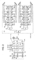
- Figure 2 illustrates an embodiment of a read data buffer 163 that may be used to implement the read data pipe 109 of Figure 1 and its interconnection to core access signal lines 170 (i.e., forming a core access path that corresponds to core access path 140) and to a data interface 161.
- the read data buffer 163 includes a load control logic circuit 169 (LC Logic) and a set of sixteen serializing buffers 171 0 -171 15 .
- Each of the serializing buffers 171 includes inputs coupled to a respective set of sixteen of the core access signal lines 170 to receive incoming read data, and an output coupled, via a single-bit signal path (172), to a respective output driver 165 within the data interface 161.
- the core access signal lines 170 includes a total of 256 signal lines for conveying read data 256 bits at a time to the read data buffer 163 as rapidly as the memory core cycle time (i.e., time between successive column operations) permits.
- the core access signal lines 170 may include more or fewer signal lines and/or the read data buffer 163 may include more or fewer serializing buffers 171, each having a storage capacity according to the number of incoming core access signal lines.
- each output driver 165 is coupled to a signal pad 166 (or to two signal pads in a differential signaling embodiment) to enable its connection to an external signaling link.
- each signal pad 166 (or pair of signal pads in a differential signaling embodiment) is additionally coupled to a signal receiver (not shown in Figure 2 ) to enable reception of incoming write data.
- the load control logic 169 is coupled to receive load control signals (LC), prefetch mode signals (PM) and sub-prefetch address signals (SPA) from the request logic (e.g., element 105 of Figure 1 ) and outputs a common set of load-shift-hold signals (LSH) and data-select signals (DS) to each of the serializing buffers 171 0 -171 15 .
- LC load control signals
- PM prefetch mode signals
- SPA sub-prefetch address signals
- LSH load-shift-hold signals
- DS data-select signals
- each of the serializing buffers 171 includes a set of sixteen storage elements, 181 0 -181 15 , to capture data from the data-sourcing set of sixteen core access signal lines, d0-d15 (more or fewer storage elements may be provided according to the number of core access signal lines in alternative embodiments), data-selecting multiplexers 183 0 -183 3 and 185 0 -185 3 , and load-control multiplexers 187 0 -187 15 (only two of which are explicitly enumerated in Figure 2 ).
- the data-selecting multiplexers 183, 185 are provided to route incoming read data (i.e., received via core access signal lines d0-d15) to selected storage elements 181 in accordance with the prefetch mode indicated by the prefetch mode signals, PM. More specifically, the load control logic 169 outputs the data-select signals, DS, to the data-selecting multiplexers 183, 185 in a state that establishes the data loading arrangement indicated by the prefetch mode signals, PM.
- the load-control multiplexers 187 are set in response to the load-shift-hold signals, and determine which of the storage elements are loaded in a given data load operation in accordance with the load-control signals, LC, and the prefetch mode indicated by the prefetch mode signals, PM.
- the prefetch mode signals specify one of three prefetch modes in which different amounts of data are retrieved from the memory core and stored within the read data pipe during a column read operation: a full prefetch mode in which a full 256 bits of data is loaded from the entire set of core access signal lines 170 into the complete set of storage elements 181 0 -181 15 within serializing buffers 171 0 -171 15 ; a first partial prefetch mode in which 128 bits of data is loaded from half the core access signal lines 170 into half the storage elements 181 within each of the serializing buffers 171 0 -171 15 (i.e., each serializing buffer 171 receiving and storing 8 bits instead of 16 bits); and a second partial prefetch mode in which 64 bits of data is loaded from one-fourth of the core access signal lines 170 into one-fourth of the storage elements 181 within each of the serializing buffers 171 0 -171 15 (i.e., each serializing buffer 171 receiving and storing 4 bits instead of 16 bits).
- prefetch modes referred to herein as x16, x8 and x4 prefetch modes to indicate the amount of data stored within each of the serializing buffers and output on each signal line of the external signal path during a given memory read operation, are assumed in connection with a number of embodiments described herein, though more or fewer prefetch modes in which larger or smaller quantities of data are retrieved from or supplied to the memory core may be supported in alternative embodiments.
- the request logic when the prefetch data becomes valid on the core access signal lines 170 (i.e., during a memory read operation), the request logic asserts a load command on the load control signal lines (i.e., the signal lines used to convey the load control signals, LC, including the load command) to enable the amount of data indicated by the prefetch mode signals, PM, to be loaded into the read data buffer 163.
- the load control signal lines i.e., the signal lines used to convey the load control signals, LC, including the load command
- the load control logic 169 outputs data-select signals to multiplexers 183 0 -183 3 and 185 0 -185 3 to route data arriving on each set of core access signal lines d0-d15 to storage elements S 0 -S 15 , respectively, within a corresponding serializing buffer 171, and the outputs load-shift-hold signals, LSH, in the load state so that each of load-control multiplexers 187 0 -187 15 passes the data arriving on a respective one of core access signal lines d0-d15 to the data input of the corresponding storage element 181.
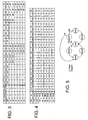
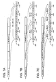
- FIGs 3 and 4 which illustrate the selections made within the data-selecting multiplexers 183, 185 and load-control multiplexers 187, respectively, in response to the control signals supplied to the load control logic 169, in the x16 prefetch mode
- the load-control multiplexers 187 are set to pass the data signals to the data inputs of the storage elements 181 0 -181 15 when the load control signals (LC) indicate a buffer load operation. That is, the data signal present at load input 'L' of each load-control multiplexer 187 is passed through the multiplexer to the data input of the corresponding storage element 181.
- read data is loaded from only a fraction of the core access signal lines d0-d15 into a corresponding fraction the storage elements within each serializing buffer 171, and the subprefetch address signals (SPA) are used to identify (or select) the subset of core access signal lines used to convey read data.
- SPA subprefetch address signals
- data-select signals are supplied to multiplexers 183 0 -183 3 and 185 0 -185 3 within each serializing buffer 171 to switchably connect core access signal lines d0-d3 and d8-d 11 to the load-control multiplexers 187 for storage elements 181 0 -181 3 and 181 8 -181 11 (S0-S3 and S8-S11), respectively.
- multiplexers 183 0 -183 3 and 187 0 -187 3 pass the data on the other set of eight core access signal lines, d4-d7 and d12-d15, to the load-control multiplexers 187 for storage elements 181 0 -181 3 and 181 8 -181 11 (S0-S3 and S8-S11), respectively.
- data-select signals are supplied to multiplexers 183 0 -183 3 to switchably connect core access signal lines d0-d1 and d8-d9 to the load-control multiplexers 187 for storage elements 181 0 -181 1 and 181 8 -181 9 (S0-S1 and S8-S9), respectively.
- multiplexers 183 0 -183 3 pass the data on core access signal lines d2-d3/d10-d11, d4-d5/d12-d13 or d6-d7/d14-d15, respectively, to the load-control multiplexers 187 for storage elements 181 0 -181 1 and 181 8 -181 9 .
- the storage elements 181 are coupled to one another through load-control multiplexers 187 to form a four-bit wide first-in-first-out (FIFO) shift register having storage elements 181 0 , 181 1 , 181 8 and 181 9 (S0, S1, S8 and S9) at the head of the queue.
- FIFO first-in-first-out
- Select signals, ss0 and ss1 are provided to multiplexers 189, 191 and 193, as shown, to pick one of head-of-queue storage elements 181 0 , 181 1 , 181 8 and 181 9 to supply data to the corresponding output driver 165 during a respective transmission interval.
- the contents of some or all of the storage elements 181 are shifted forward within each of the serializing buffers 171 0 -171 15 after data initially loaded into the head-of queue storage elements has been transmitted.
- the x 16 prefetch mode when the x 16 prefetch mode is selected, three shift operations are performed in succession following each data load operation to forward the data in second-stage, third-stage and fourth-stage storage element groups (i.e., storage elements S2/S3/S10/S11, S4/S5/S12/S13 and S6/S7/S14/S15, respectively) to the head of the queue.
- the data to be shifted is passed through the shift port (S) of the load-control multiplexer 187 disposed between the output node of a given storage element 181 and the input node of the next-stage storage element 181.
- the group of storage elements to which the final-stage data has been shifted need not be the recipient of further incoming shifted data, and thus may be placed in a data hold state during subsequent data shift cycles to save power.
- data need not be shifted into the fourth-stage storage elements (S6/S7/S14/S15), so that no data need be shifted into the fourth-stage storage elements (note that, in an alternative embodiment, the shift input may be omitted from the load-control multiplexers 187 for the fourth-stage storage elements S6/S7/S14/S15).
- the shift input path (S) through each of the load-control multiplexers 187 is selected for the first, second, and third stage storage elements (S0-S5 and S8-S13), while the fourth-stage storage elements are maintained in a hold state (H).
- the shift input path through each of the load-control multiplexers 187 is selected for the first stage storage elements (S0/S1/S8/S9) only, with all other storage elements left in the hold state. No shifting occurs in the Figure 2 embodiment in the x4 prefetch mode.
- the core cycle time (i.e., time between successive column access operations) remains fixed as different prefetch modes are selected, thus leading to unused transmission bandwidth on the external data path in partial prefetch modes. That is, when a full (e.g., x16) prefetch mode is selected, data retrieved from the memory core is loaded into the full set of storage elements within each of the serializing buffers 171 0 -171 15 and then shifted out in a sequence of three shift operations (each shift following the transmission of the four bits in the first-stage storage elements S0/S1/S8/S9), thus consuming the entire data path bandwidth before transmitting the read data for a subsequent read access (or write data for a subsequent write access).
- a full prefetch mode e.g., x16
- the state machine starts from the load state (Load) in which data is loaded into all or a subset of storage elements within the serializing buffers 171 of Figure 2 .
- the state machine progresses to Hold1, Hold2 and Hold3 states before returning to the Load state to load the next set of x4 prefetch data.
- the Hold1, Hold2 and Hold3 states all the storage elements 181 within the serializing buffers 171 are maintained in a hold state to save power.
- the state machine progresses from the Load state to a Shift1 state (i.e., to shift data from the second-stage storage elements to the first-stage storage elements within each of the serializing buffers), and then the Hold2 and Hold3 states before returning to the Load state to load the next set of x8 prefetch data.
- Shift1 state i.e., to shift data from the second-stage storage elements to the first-stage storage elements within each of the serializing buffers
- the state machine progresses from the Load state to Shift1, Shift2 and Shift3 states before returning to the load state to load the next set of x 16 prefetch data, thus enabling read data to be shifted forward from the fourth-stage storage elements 181 to the first stage storage elements 181 in a sequence of three data shift operations within the serializing buffers 171.
- a hold state may also be entered if no memory read requests are being serviced within a given request cycle.
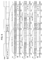
- Figure 6 illustrates exemplary data transmission sequences at the sixteen input/output (I/O) nodes of the data path interface (i.e., element 161 of Figure 2 ) for the x16, x8 and x4 prefetch modes.
- I/O input/output
- MR REQn memory read request
- CCLK rising edge of core cycle clock
- a load operation occurs at time 221 (i.e., at the conclusion of the transmission of a prior set of x16 prefetch data), followed by transmission of the contents of first-stage serializing buffer storage elements S0/S1/S8/S9 over the next four data transmission intervals.
- a first shift operation is carried out within the serializing buffers to advance the contents of the S2/S3/S10/S11 storage elements to the head-of-queue position (and to advance the contents of the third-stage and fourth-stage storage elements to the second-stage and third-stage storage elements, respectively) and thus, as shown, the contents of the S27S3/S10/S11 are transmitted in the next four data transmission intervals.
- a second shift operation is carried out within the serializing buffers to advance the contents originally loaded into the third-stage storage elements, S4/S5/S12/S 13, to the head-of-queue position for transmission during the next four transmission intervals.
- a third shift operation is carried out within the serializing buffers to advance the contents originally loaded into the fourth-stage storage elements, S6/S7/S14/S15, to the head-of-queue position for transmission during the final four transmission intervals for the memory access request.
- a load operation may be performed to load the next set of x 16 prefetch data into the read data pipe in response to memory request, MR REQ n+1, so that data transmission may continue without interruption.
- a load operation occurs at time 231 to load a x8 prefetch data set into the first-stage and second-stage storage elements within the read data pipe, followed by transmission of the contents of first-stage storage elements, S0/S1/S8/S9, over the next four data transmission intervals.
- a first shift operation is carried out within the serializing buffers to advance the contents of the second-stage storage elements (S2/S3/S10/S11) to the head-of-queue position for transmission over the next four data transmission intervals.
- the memory read operation is complete and the external data path remains idle over the next eight transmission intervals as additional read data is retrieved from the memory core (i.e., in a back-to-back memory read).
- the data load operation in the x8 mode may be limited to the first-stage and second-stage storage elements within the read data pipe and no shifting of data into the third-stage storage elements is necessary during the shift operation.
- the state of all the storage elements in the read data pipe may be held constant during the unused transmission intervals (e.g., by gating the clocking signal or by switching the storage element output to the storage element input) to save power. This operation is indicated in Figure 6 by the hold operations at times 235 and 237.
- a load operation may be performed to load the next set of x8 prefetch data into the read data pipe in response to memory request, MR REQ n+1.
- a load operation occurs at time 241 to load a x4 prefetch data set into the first-stage storage elements, S0/S1/S8/S9, within the read data pipe, followed by transmission of the contents of first-stage storage elements over the next four data transmissions intervals.
- the memory read operation is complete and the data path remains idle over the next twelve transmission intervals as additional read data is retrieved from the core (i.e., in a back-to-back memory read).
- the data load operation in the x4 mode may be limited to the first-stage storage elements within the read data pipe.
- the state of all the storage elements in the read data pipe may be held constant during the unused transmission intervals (e.g., by gating the clocking signal or by switching the storage element output to the storage element input) to save power.
- This operation is indicated in Figure 6 by the hold operations at times 243, 245 and 247.
- a load operation may be performed to load the next set of x4 prefetch data into the read data pipe in response to memory request, MR REQ n+1.
- Figures 7A-7C illustrate operation within an alternative embodiment of a memory device in which core cycle times may be adjusted in response to different prefetch mode selections to avoid unused data path bandwidth.
- Figure 7A illustrates the data transmission sequence in the full prefetch mode (i.e., x16 prefetch mode) described in reference 220 of Figure 6 though, for simplicity, data transmission over a single data link is shown instead of the full set of N transmissions over N data links.
- Figure 7B illustrates a data transmission sequence 260 in a x8 prefetch mode in which memory read requests (MR REQn, MR REQn+1, MR REQn+2, ...) are received at twice the rate as in the x16 prefetch mode, and in which the core cycle time is correspondingly halved relative to the x 16 prefetch mode. Because the core cycle time has been halved, requests may be serviced at twice the rate, but half the granularity (x8) of the full (x16) prefetch mode.
- a x8 read data set (RD n) that corresponds to memory read request n (MR REQn) is loaded into a subset of storage elements within the read data pipe at time 261, and shifted out over the next eight transmission intervals (i.e., with second-stage data being shifted to the head of queue at time 263).
- a new load operation occurs to capture the x8 read data set (RDn+1) that corresponds to memory read request n+1 (i.e., in a back-to-back read), with the data set being transferred in the immediately ensuing eight transmission intervals so that; despite the finer (reduced) data access granularity, no data path bandwidth is unused.
- a data transmission sequence 270 for the x4 prefetch mode illustrated in Figure 7C
- memory access requests are received at four times the rate as in the x16 prefetch mode and the core cycle time is correspondingly reduced by a factor of four relative to the x16 prefetch mode, thus enabling memory access requests to be serviced at four times the rate, but one-fourth the granularity (x4), of the full (x16) prefetch mode.
- RD n x4 read data set
- MR REQn memory read request n
- a new load operation to capture the x4 read data set (RDn+1) that corresponds to memory read request n+1 (i.e., in a back-to-back read), with the data set being transferred in the immediately ensuing four transmission intervals so that, despite the finer data access granularity, the full data path bandwidth is consumed.
- data sets RDn+2 and RDn+3 are transferred, in response to memory read requests n+3 and n+4, in immediately sets of four transmission intervals.
- Figure 8 illustrates embodiments of a column decoder 301 and column multiplexers 305 0 -305 K-1 (ColMux 0 - ColMux K-1) that may be used in the memory device of Figure 1 to selectively couple sense amplifiers within storage banks 131 0 -131 K-1 to the core access path 140.
- column multiplexers 305 0 -305 K-1 are coupled respectively between the sense amplifier banks 303 0 -303 K-1 (SA Bank 0 - SA Bank K-1) that correspond to the K storage banks 131 of Figure 1 and the core access path 140.
- Each of column multiplexers 305 is further coupled to receive a column select signal 324 from the column decoder 301 which, as shown in detail view of column multiplexer 305 0 , includes J sets of prefetch select lines 325 0 -325 J-1 .
- the column decoder 301 includes bank-address decode logic 331 and column select logic circuits 333 0 -333 K-1 , and is coupled to receive a bank address (BA), column address (CA) and sub-prefetch address (SPA), as well as the prefetch mode signals (PM) and a decode enable signal (DE), from the request logic.
- BA bank address
- CA column address
- SPA sub-prefetch address
- PM prefetch mode signals
- DE decode enable signal
- bank-address decode logic 331 decodes the bank address to activate the bank-address-specified one of K bank enable lines 322 0 -322 K-1 that are coupled respectively to bank-enable inputs (be) of column select logic circuits 333 0 -333 K-1 .
- each of the column select logic circuits 333 includes a column-address decoder 337 that, in response to activation of the corresponding bank enable line 322, decodes the column address to activate the column-address-specified one of J column-enable lines 338.
- Each column select logic circuit 333 further includes a set of J sub-prefetch decoders 335 0 -335 J-1 coupled to receive the subprefetch address and having column-enable inputs (ce) coupled respectively to the J column-enable lines 338.
- the sub-prefetch decoder 335 activates one or more of prefetch select lines a, b, c and d within the corresponding set of prefetch select lines 325.
- each of the transfer gate circuits 317 includes a set of sixteen subprefetch-gate circuits 319 0 -319 15 each of which includes sixteen pass-gate configured transistors coupled between a respective column 315 of sixteen sense amplifiers (SA) and a corresponding set of sixteen core access signal lines within core access path 140.
- SA sense amplifiers
- each four-transistor group referred to herein as a quad gate 321
- SA sense amplifiers
- the gate terminals of the transistors 320 within each quad gate 321 are coupled in common to a respective one of four prefetch select lines 325 from a corresponding sub-prefetch decoder 335.
- each of the quad gates 321a-321d may be switched to a conducting state through activation of a corresponding one of the four prefetch select lines to form a continuous signal path (i.e., switched connection) between the corresponding set of four sense amplifiers 317 and respective core access signal lines.
- the prefetch mode signals (PM) and subprefetch address signals (SPA) are supplied to each of the subprefetch decoders 335 to control the number of activated quad gates and, in a partial prefetch mode, the subset of quad gates to be activated during a given column access operation.
- a subprefetch decoder 335 coupled to an activated column-enable line 338 i.e., an address-selected subprefetch decoder 335 will activate all four prefetch select lines 325, thus switching all four quad gates 321a-321d within a given subprefetch-gate circuit 319 to a conducting state to switchably connect the corresponding set of sixteen sense amplifiers 315 to the sixteen core access lines.
- each set of four prefetch select lines 325 extends across and is coupled in common to quad gates within each of the sixteen sub-prefetch gate circuits 319 0 -319 15 (hex-gates) so that, in the x16 prefetch mode, an address-selected column of 256 sense amplifiers (i.e., one of the sets 311 0 -311 J-1 of 256 sense amplifiers) is switchably coupled to respective signal lines of the core access path 140.
- the subprefetch decoder 335 coupled to the activated column-enable line 338 will activate two prefetch signal lines, a/b or c/d, within a selected set of four prefetch select lines 325, depending on the most significant bit of the subprefetch address (SPA[1]), thus switching on two of the four quad gates 321a-321d within each of sub-prefetch gate circuits 319 0 -319 15 and establishing a connection between a column of 128 sense amplifiers (i.e., within one of the 256-sense amplifier sets 311 0 -311 J-1 ) and a 128-line subset of the core access signal lines.
- SPA[1] most significant bit of the subprefetch address
- the subprefetch decoder 335 coupled to the activated column-enable line 338 will activate one of the four prefetch signal lines (a, b, c or d), within a selected set of four prefetch select lines 325, depending on the two bits of the subprefetch address, thus switching on one of the four quad gates 321a-321d within each of sub-prefetch gate circuits 319 0 -319 15 and establishing a connection between a column of 64 sense amplifiers and a 64-line subset of the core access signal lines.
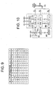
- Figure 9 illustrates an exemplary decoding operation performed by each of the subprefetch decoders 335 of Figure 8 .
- the column-enable input, ce is a logic '0' (i.e., corresponding column-enable line 338 is deactivated)
- none of the prefetch signal lines (a, b, c, d) is activated, regardless of the prefetch mode (PM) and the subprefetch address (SPA); the prefetch mode and subprefetch address thus being designated by don't care symbol 'X'.
- FIG 10 illustrates an embodiment of a write data buffer 363 that may be used to implement the write data pipe 111 of Figure 1 .
- the write data buffer 363 includes framing control logic 369 and a set of deserializing buffers 371 0 -371 15 , each coupled to a respective write data receiver 365 (which, for example, samples the signal arriving at pad 166 in response to a receive clock rClk) within the data interface 361.
- each of the deserializing buffers 371 0 -371 15 performs the inverse function of the serializing buffers 171 described in reference to Figure 2 , receiving a serial stream of 16, 8 or 4 bits per memory write operation according to the prefetch mode, PM (longer or shorter bitstreams may be received in alternative embodiments that support other prefetch modes), and framing the bits in corresponding 4-bit, 8-bit or 16-bit wide data values, referred to herein as data frames, that are driven onto respective sets of 4, 8 or 16 core access signal lines within core access path 140.
- the framing control logic 369 controls the time at which data frames are driven onto the core access signal lines, and the prefetch mode (PM) and subprefetch address (SPA) are used to select, through generation of load-shift-hold signals (LSH) and data-select signals (DS) within the framing logic 369, which storage elements within the write data buffer 363 are loaded with incoming write data bits and which core access signal lines are driven with bits of a given data frame.
- PM prefetch mode
- SPA subprefetch address
- LSH load-shift-hold signals
- DS data-select signals
- each deserializing buffer 371 of the write data buffer 363 is loaded with bits of a 16-bit data frame, and then driven onto a corresponding set of sixteen core access signal lines, thus providing a 256 bit write data value on the core access signal path.
- each deserializing buffer 371 When, a x8 prefetch mode is selected, half the storage elements within each deserializing buffer 371 are loaded with bits of an 8-bit data frame, and then used to drive (i.e., switchably connected to) one of two sets of 8 core access signal lines (i.e., within the set of sixteen core access signal lines that corresponds to the deserializing buffer 371) according to the most significant bit of the subprefetch address, SPA.
- a x4 prefetch mode When a x4 prefetch mode is selected, one-fourth of the storage elements within each deserializing buffer 371 are loaded with bits of a 4-bit data frame, and then used to drive one of four sets of 4 core access signal lines according to the two-bit subprefetch address, SPA.
- write masking information may also be received via the data interface, with write masking bits indicating which bytes (or other data segments) of the incoming data are to be written to the memory core.
- the deserializing buffers 371 may selectively drive core access lines in response to both the write masking bits and the selected prefetch mode.
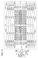
- FIG 11 illustrates an embodiment of a memory device 375 having circuitry to support scaled prefetch modes as well as mode-selectable data transfer rates and data access timing.
- memory device 375 is a dynamic random access memory (DRAM) device having eight, separately accessible DRAM storage banks (B0-B8), each partitioned into cater-comer -A and -B sub-banks.
- the even-numbered storage banks (B0, B2, B4, B6) are disposed opposite the odd-numbered storage banks (B1, B3, B5, B7) about a central data input/output (I/O) interface 377, thus forming four sub-bank quadrants 376A EVEN , 376B EVEN , 376A ODD and 376B ODD .
- Each sub-bank quadrant 376 is coupled via a respective set of core access signal lines, 170A EVEN , 170B EVEN , 170A ODD and 170B ODD , to a respective data pipe 381A EVEN , 381B EVEN, 381A ODD AND 381B ODD .
- each of the data pipes 381 includes a set of eight I/O buffers 382, with each I/O buffer 382 coupled between a respective 16-line subset of the core access signal lines 170 and a one-line connection to a corresponding data I/O circuit (shown in Figure 11 and referred to herein as "DQ") within I/O circuit bank 380A or 380B.
- DQ data I/O circuit
- each DQ is shared by odd and even sub-banks and may include a multiplexer/demultiplexer 379 as shown in detail view 378 to select between corresponding even and odd I/O buffers as a transmit data source or receive-data destination.
- Read data and other out-bound data is output from the memory device 375 via I/O node 166 by output driver 165 in response to transitions of a transmit clock signal (tClk), while write data and other in-bound data is received within the memory device via I/O node 166 by signal receiver 365 in response to transitions of a receive clock signal (rClk).
- tClk transmit clock signal
- rClk receive clock signal
- the transmit and receive clock signals may be aperiodic timing signals such as strobe signals and may be supplied from an external source or derived from an externally supplied timing signal. Further, in one embodiment, the transmit and receive clock signals are phase aligned (and may be the same clock signal or generated by a clock tree circuit to establish phase alignment) with each other and/or with an externally supplied clock signal so that a single clock domain applies within the memory device.
- the even-bank row decoder circuits RDA EVEN and RDB EVEN are coupled to receive the same incoming address and control signals from a request controller and the even-bank column decoder circuits CDA EVEN and CDB EVEN are likewise coupled to receive the same incoming address and control signals (not shown in Figure 11 ), so that the even-bank decoder circuits operate in lock step to enable simultaneous access to both sub-banks of an even-numbered storage bank.
- the odd-bank decoder circuits may also be coupled to receive the same incoming address and control signals from the request controller and thus operate in lock step to enable simultaneous access to both sub-banks of an odd-numbered storage bank.
- each of the column decoder circuits and each of the row decoder circuits may be operated independently, to enable independent access to each sub-bank quadrant 376.
- the even-bank and odd-bank row decoder circuits are coupled to receive bank address and row address values from the request logic and thus each activate one address-selected word line within respective sets of word lines 134A EVEN , 134B EVEN , 134A ODD and 134B ODD to carry out row activation and precharge operations in the address-selected bank and row of the corresponding sub-bank quadrant 376.
- the even-bank and odd-bank column decoder circuits are coupled to receive bank address and column address values and thus provide column multiplexing signals 136A EVEN , 136B EVEN , 136A ODD and 136B ODD to couple an address-selected column of sense amplifiers within an address-selected bank to the core access signal lines 170 for the corresponding sub-bank quadrant 376.
- a prefetch mode value may be programmed within a configuration circuit (e:g., a mode register) of the memory device 375 or otherwise supplied to the memory device to control the number of column access signal lines 170 used to receive data from or deliver data to an address selected column of sense amplifiers, and to control the number of storage elements within the I/O buffers 382 that are loaded with read data or write data.
- a configuration circuit e:g., a mode register
- the even and odd storage banks are coupled in parallel to I/O circuit banks 380A and 380B.
- the distinct access paths formed by the parallel-coupled even and odd storage banks is exploited to achieve reduced data transfer granularity in an operating mode referred to herein as a micro-thread mode. More specifically, in a first operating mode referred to herein as a single-thread mode (or single-thread mode), either an odd numbered storage bank or an even numbered storage bank is accessed over the entire duration of a column access cycle, referred to herein as a T CC interval.
- the T CC interval is split between accesses to odd and even numbered storage banks, with one resource (an odd or even numbered storage bank) accessed during a first portion of the T CC interval and another resource (an even or odd numbered storage bank) accessed during a second portion of the T CC interval.
- the sub-bank quadrants are accessed independently of one another to provide four distinct memory resources that may be accessed in respective portions of a T CC interval.
- the T CC interval may be further subdivided as additional independently accessible (e.g., independently addressable) memory resources are provided.
- the memory device 375 includes a configuration circuit (e.g., a volatile or non-volatile mode register) which may be loaded (i.e., programmed) with mode selection information including a clock-to-core ratio in the form of a T CC count value that indicates the minimum number of clock cycles per T CC interval (and thus a clock frequency for a specified T CC interval), and a thread mode value that indicates the number of column access operations to be performed per T CC interval.
- the mode selection information may further include a data rate specifier that indicates the number of data bits transferred per clock cycle (data rate may alternatively be fixed by design) and/or a prefetch mode value to indicate the number of data bits transferred to or from the memory device per column access operation per data I/O node.
- the prefetch mode drops to 8 bits per DQ per column access operation.
- the thread mode may be increased to 4 (e.g., where individual sub-bank quadrants are accessed at respective column addresses) or any other number that is supported by independently accessible memory resources within the memory device.
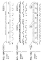
- Figures 12A-12C illustrate memory access modes that may be selected or programmed within the memory device 375 of Figure 11
- Figures 13A-13C illustrate corresponding request and data transfer operations in the different memory access modes.
- the memory access granularity i.e., amount of data retrieved or written per column access operation
- load and shift operations are carried out as described in reference to the x16 prefetch mode operation of Figure 6 , with a buffer load occurring at the start of each new T CC time interval, followed by three shift operations spaced at two transmit clock cycle intervals.
- a x8 prefetch mode is established as eight bits of data are loaded into an I/O buffer 382 per column access operation.
- the full bandwidth of the signaling path is consumed by read or write data transfer due to transmission of data to or from the alternate memory resource in the second half of the T CC interval.
- column access requests are provided twice as frequently as in the single-thread mode example of Figures 12A and 13A , with column access requests being directed alternately to resource X and resource Y (i.e., col reqX n, col reqY n, col reqX n+1, etc.).
- resource X and resource Y i.e., col reqX n, col reqY n, col reqX n+1, etc.
- Half the storage elements within the deserializing buffers 371 of Figure 10 are likewise loaded in per column write operation. As in the x8 prefetch mode discussed in reference to Figure 6 , only half the column access lines need be driven by read or write data during a given column access operation. Overall, the micro-thread mode of operation enables the full bandwidth of the data path to be consumed with read and write data transfers, but with memory access granularity reduced to 8 bits per DQ or, in the 16-DQ embodiment of Figure 11 ,16 bytes total.
- a full x16 prefetch mode is established as sixteen bits of data are loaded into an I/O buffer 382 per column access operation.
- the micro-thread memory access permits the data transfer rate on the signaling path to be doubled without necessitating a doubling of internal data transfer resources of the memory device.
- column access requests are provided twice as frequently as in the single-thread mode example of Figures 12A and 13A , with column access requests being directed alternately to resources X and Y (i.e., col reqX, col reqY, col reqX, col reqY, etc.).
- the request signaling rate is assumed to scale with the data transfer rate (i.e., request signaling rate also doubled) so that requests are transferred over intervals that are one half as long as those in Figure 12A , thus leaving relatively the same amount of request path bandwidth. Also, because a full x16 prefetch operation and corresponding 16-bit data transmission per DQ is completed twice per T CC . interval, the rate at which the load-control state machine (e.g., as described in reference to Figure 5 ) transitions from state to state is doubled.
- the clocking rate of the load-control state machine may be controlled by the T CC count programmed within the memory device or directly by a frequency divided version of the transmit/receive clock signals (or signals having a frequency relation thereto).
- micro-thread mode of operation shown in Figures 12C and 13C enables the full bandwidth of the data path to be consumed at the increased signaling rate without increasing the column access granularity relative to the operating mode of Figures 12A and 13A (i.e., column access granularity remains at 16 bits per DQ despite the doubling of net data transferred).
- doubling the data transfer rate would necessitate doubling of the column access granularity in order to consume the full data path bandwidth (i.e., increasing column access granularity to 32 bits per DQ or, in the embodiment of Figure 11 , 64 bytes total) and, in turn, require corresponding increase in data transfer resources within the memory device.
- the read and write data buffer sizes and number of core access lines would double. This result is particularly undesirable in applications that do not benefit from larger column access granularity (e.g., where relatively small, dispersed data accesses are needed).
- the micro-threading operation permits signaling rate increases and correspondingly increased memory bandwidth without increase in memory access granularity.
- the thread mode may be established by the T CC count value programmed within the configuration register. More specifically, when the T CC count value specifies a clock frequency so limited as to require substantially the entire T CC interval to complete a read or write operation directed to a given storage resource (e.g., entire T CC interval required transmit data prefetched from an addressed resource), the request logic within the memory device may automatically operate in a single-thread mode to permit random access to any bank, sub-bank or other resource of the storage array.
- the memory device may automatically operate in a multi-thread mode in which prefetch operations (or data write operations) are interleaved between multiple distinct resources in each T CC interval, with each such resource being independently addressed.
- prefetch operations or data write operations
- memory access requests are directed, without address limitation, to a single memory bank or other storage resource per T CC interval.
- the memory device will operate in a single-thread mode, transferring data associated with each controller-supplied address between the data I/O buffers 382 and I/O signaling interface (i.e., data I/O circuits, DQ) during each of N cycles of the clock signal.
- N an integer value
- DQ data I/O circuits
- the memory device may transfer data associated with a first address between the data I/O buffers 382 and the data I/O circuits during each of X cycles of the clock signal (X ⁇ N) and immediately thereafter transfer data associated with one or more additional addresses between the data I/O buffers 382 and the data/O circuits during each of an additional set of X cycles of the clock signal.
- the ratio of N to X corresponds to the thread mode established within the memory device (e.g.,.
- the memory controller may determine the T CC count values that correspond to the different thread modes of the memory device, for example, by obtaining or determining the T CC interval (and data rate and/or prefetch size) of the memory device from information stored within a serial presence detect memory or other characterizing storage device.
- the memory controller may issue a TCC count value (or other value that indicates a desired clock-to-core ratio) to the memory device in association with one or more instructions to store the TCC count value within a configuration register (e.g., a mode register) of the memory device, and thus establish a desired clock-to-core ratio therein.
- a configuration register e.g., a mode register
- the clock-to-core ratio e.g., T CC count value
- the clock-to-core ratio may be automatically established according to the thread mode, prefetch mode and data rate programmed (or fixed by design) within the memory device.
- the T CC count value has been described as specifying the number of cycles of a transmit or receive clock cycle per T CC interval, the T CC count value may alternatively specify the number of cycles of a reference clock signal or master clock signal provided to or generated within the memory device.
- a master clock signal is provided to the memory device from an external source (e.g., a memory controller) and used to establish a unified clock domain within the memory device.
- separate clock signals and/or strobe signals may be transmitted between the memory device and memory controller to time the transmission and reception of data, with such signals having a frequency (or a peak toggle rate in the case of a strobe signal) that is the same as or a multiple (including a fractional multiple) of the master clock signal.
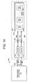
- Figure 14 illustrates an embodiment of a data processing system 400 having a processor 401 (or any other memory access requestor) and a memory subsystem 405 that supports selectable prefetch modes and clock-to-core ratios.
- the memory subsystem 405 includes a memory controller 407 coupled to one or more memory modules 421a-421n, with each memory module 421 including one or more memory devices 425a-425m (e.g., discrete integrated circuit devices) and, optionally, a serial-presence detect 427 memory (SPD) or other non-volatile storage that provides characterizing information for the corresponding memory devices 425.
- SPD serial-presence detect 427 memory
- the characterizing information may specify the prefetch mode capability of the corresponding memory devices 425 (e.g., that the memory devices 425 have multiple prefetch modes and their respective prefetch sizes, and/or that the core cycle times of the memory devices may be increased in one or more partial prefetch modes to avoid unused data path bandwidth) in addition to storage capacity, maximum operating frequency and/or other memory device characteristics.
- the characterizing information may further specify thread modes that are available within the memory devices, as well as T CC count ranges supported by the memory devices.
- the memory controller 407 may read the characterizing information from the SPD 427 for each memory module 421 (or an SPD or like device for the set of memory modules) and identify one or more memory modules 421 as supporting scaled prefetch modes, multiple thread modes and/or multiple T CC count values. In one embodiment, the memory controller 407 may program prefetch modes, thread modes and/or T CC count values within the memory devices 425 (or subset thereof) according to application needs or to establish uniform operation over all the memory modules 421.
- the memory controller 407 may program configuration registers within the memory devices 425 of the scaled-prefetch memory modules to establish uniform prefetch sizes across the memory devices 425 within each of the memory modules 421.
- the memory controller 407 may program configuration registers within the memory devices 425 of the micro-threading memory modules to establish uniform clock-to-core ratios and/or thread modes within each of the memory modules 421.
- the memory controller 407 (or processor) may allocate data storage within the memory modules according to prefetch-mode scalability and/or micro-threading capability.
- the processor 401 may instruct the memory controller 407 to allocate storage within the scaled-prefetch, micro-threading memory modules to graphics applications or other applications programs that may benefit from finer-grained data prefetch and column access granularity.
- the memory controller 407 may dynamically transition the memory module 421 or any of the memory devices 425 thereon between various modes, for example, in response detecting a threshold density of fine-grained memory access requests (i.e., a threshold number of such access requests within a given time interval or a threshold percentage of total memory access requests) from the processor/requestor 401 or in response to an explicit mode command from the processor/requestor 401.
- a threshold density of fine-grained memory access requests i.e., a threshold number of such access requests within a given time interval or a threshold percentage of total memory access requests
- a request generator 413 is provided to generate memory access requests and operational requests to configure the memory devices (including programming prefetch modes), read the SPD, perform signaling calibration, refresh operations, and so forth, in response to access requests from the processor 401 received via host interface path 402 (which may include separate data and request components as shown or a time-multiplexed path).
- a data pipe 409 is provided to buffer read and write data associated with the memory access requests and or data associated with configuration operations.
- Signaling path 408 may include one or more clock and/or strobe signal lines to convey timing signals (e.g., a reference clock signal or master clock signal) for timing the receipt of signals within the memory devices 425 and/or memory controller 407 and to establish synchronous operation within the memory devices 425.
- each of the memory devices 425 includes clock recovery circuitry to recover a clock signal from one or more signals transmitted via signaling path 408.
- memory modules 421 are depicted in Figure 14
- the memory devices 425 may be mounted directly to a mother board or integrated into a multi-chip module along with the memory controller 407 and/or processor 401 to form, for example, a system-in-package (SIP) DRAM system.
- the data path and request path (collectively, 408) coupled between the memory devices 425 (or memory modules) and the memory controller 407 may be implemented using virtually any signaling channel, including an electronic conduction path, an optical path or wireless signaling channel.
- the processor 401, memory controller 407, and/or one or more of memory devices 425 may be combined on a single integrated circuit die in an alternative embodiment.
- circuits disclosed herein may be described using computer aided design tools and expressed (or represented), as data and/or instructions embodied in various computer-readable media, in terms of their behavioral, register transfer, logic component, transistor, layout geometries, and/or other characteristics. Formats of files and other objects in which such circuit expressions may be implemented include, but are not limited to, formats supporting behavioral languages such as C, Verilog, and HLDL, formats supporting register level description languages like RTL, and formats supporting geometry description languages such as GDSII, GDSIII, GDSIV, CIF, MEBES and any other suitable formats and languages.
- Computer-readable media in which such formatted data and/or instructions may be embodied include, but are not limited to, non-volatile storage media in various forms (e.g., optical, magnetic or semiconductor storage media) and carrier waves that may be used to transfer such formatted data and/or instructions through wireless, optical, or wired signaling media or any combination thereof.
- Examples of transfers of such formatted data and/or instructions by carrier waves include, but are not limited to, transfers (uploads, downloads, e-mail, etc.) over the Internet and/or other computer networks via one or more data transfer protocols (e.g., HTTP, FTP, SMTP, etc.).
- Such data and/or instruction-based expressions of the above described circuits may be processed by a processing entity (e.g., one or more processors) within the computer system in conjunction with execution of one or more other computer programs including, without limitation, net-list generation programs, place and route programs and the like, to generate a representation or image of a physical manifestation of such circuits.
- a processing entity e.g., one or more processors
- Such representation or image may thereafter be used in device fabrication, for example, by enabling generation of one or more masks that are used to form various components of the circuits in a device fabrication process.
- circuit elements or circuit blocks may be shown or described as multi-conductor or single conductor signal lines.
- Each of the multi-conductor signal lines may alternatively be single-conductor signal lines, and each of the single-conductor signal lines may alternatively be multi-conductor signal lines.
- Signals and signaling paths shown or described as being single-ended may also be differential, and vice-versa.
- signals described or depicted as having active-high or active-low logic levels may have opposite logic levels in alternative embodiments.
- circuits described or depicted as including metal oxide semiconductor (MOS) transistors may alternatively be implemented using bipolar technology or any other technology in which a signal-controlled current flow may be achieved.
- MOS metal oxide semiconductor
- a signal is said to be "asserted” when the signal is driven to a low or high logic state (or charged to a high logic state or discharged to a low logic state) to indicate a particular condition.
- a signal is said to be “deasserted” to indicate that the signal is driven (or charged or discharged) to a state other than the asserted state (including a high or low logic state, or the floating state that may occur when the signal driving circuit is transitioned to a high impedance condition, such as an open drain or open collector condition):
- a signal driving circuit is said to "output" a signal to a signal receiving circuit when the signal driving circuit asserts (or deasserts, if explicitly stated or indicated by context) the signal on a signal line coupled between the signal driving and signal receiving circuits.
- a signal line is said to be “activated” when a signal is asserted on the signal line, and “deactivated” when the signal is deasserted.
- the prefix symbol "/" attached to signal names indicates that the signal is an active low signal (i.e., the asserted state is a logic low state).
- a line over a signal name (e.g., ' ⁇ signal name>') is also used to indicate an active low signal.
- the term “coupled” is used herein to express a direct connection as well as a connection through one or more intervening circuits or structures.
- the term “exemplary” is used to express an example, not a preference or requirement.
Landscapes
- Engineering & Computer Science (AREA)
- Microelectronics & Electronic Packaging (AREA)
- Computer Hardware Design (AREA)
- Databases & Information Systems (AREA)
- Dram (AREA)
- Memory System Of A Hierarchy Structure (AREA)
- Information Transfer Systems (AREA)
- Read Only Memory (AREA)
Claims (8)
- Speichervorrichtung (100) mit:einem Speicherarray (135); undeinem Lesedatenzwischenspeicher (163), der mit dem Speicherarray (135) über Datenleitungen (170) gekoppelt ist und eine Steuerlogik (169) zum Laden von Daten aufweist, die auf all den Datenleitungen (170) übermittelt sind, in den Lesedatenzwischenspeicher (163) in Antwort auf die Erklärung eines Ladesignales in einem ersten Prefetch-Modus;dadurch gekennzeichnet, dass
die Steuerlogik (169) ferner zum Laden von Daten, die auf einer adressausgewählten Untermenge der Datenleitungen (170) übermittelt sind, in den Lesedatenzwischenspeicher (163) in Antwort auf eine Erklärung des Ladesignales in einem zweiten Prefetch-Modus. - Speichervorrichtung (100) nach Anspruch 1, wobei das Speicherarray (135) einen Satz von Leseverstärkern zum Speichern von Daten aufweist, die von ausgewählten Speicherzellen innerhalb des Speicherarrays (135) abgerufen sind, und wobei die Datenleitungen (170) zwischen dem Lesedatenzwischenspeicher (163) und dem Satz von Leseverstärkern gekoppelt sind.
- Speichervorrichtung (100) nach Anspruch 2, ferner mit einer Spaltendekodierschaltung (115) zum schaltbaren Verbinden all der Datenleitungen (170) mit entsprechenden Leseverstärkern innerhalb des Satzes von Leseverstärkern in dem ersten Prefetch-Modus und zum schaltbaren Verbinden der adressausgewählten Untermenge der Datenleitungen (170) mit entsprechenden Leseverstärkern innerhalb des Satzes von Leserverstärkern in dem zweiten Prefetch-Modus.
- Speichervorrichtung (100) nach einem der vorstehenden Ansprüche, wobei der Lesedatenzwischenspeicher (163) eine Vielzahl von Speicherelementen zum Speichern von Lesedaten aufweist, und wobei die Steuerlogik (169) eine Multiplexerschaltung zum schaltbaren Verbinden der adressausgewählten Untermenge der Datenleitungen (170) an eine Untermenge der Vielzahl von Speicherelementen in dem zweiten Prefetch-Modus aufweist.
- Speichervorrichtung (100) nach einem der vorstehenden Ansprüche, ferner mit einem programmierbaren Register zum Speichern eines Wertes, welcher entweder den ersten Prefetch-Modus oder den zweiten Prefetch-Modus innerhalb der Speichervorrichtung (100) einrichtet.
- System mit:einem Speichercontroller;einem Signalweg (102), der mit dem Speichercontroller gekoppelt ist; undeiner Speichervorrichtung (100) nach Anspruch 1.
- Verfahren eines Betriebes innerhalb einer Speichervorrichtung (100), wobei das Verfahren aufweist:Abrufen von Daten von einem Speicherarray (135);Laden entweder eines ersten Teiles der Daten oder eines zweiten Teiles der Daten in einen Lesedatenzwischenspeicher (163) demgemäß, ob ein Prefetch-Modus-Signal einen ersten Prefetch-Modus oder einen zweiten Prefetch-Modus anzeigt, wobei der zweite Teil der Daten kleiner als der erste Teil der Daten ist; undAusgeben des Teiles der Daten, der in den Lesedatenzwischenspeicher (163) geladen ist, aus der Speichervorrichtung (100).
- Verfahren nach Anspruch 7, wobei ein Laden des ersten Teiles der Daten in den Lesedatenzwischenspeicher (163) ein Bilden eines Signalweges zwischen Leseverstärkern, welche den ersten Teil der Daten enthalten, und einer Vielzahl von Speicherelementen innerhalb des Lesedatenzwischenspeichers (163) aufweist, und wobei ein Laden des zweiten Teiles der Daten ein Bilden eines Signalweges zwischen einer adressausgewählten Untermenge der Leseverstärker und einer Untermenge der Vielzahl von Speicherelementen aufweist.
Priority Applications (2)
| Application Number | Priority Date | Filing Date | Title |
|---|---|---|---|
| EP11160777A EP2363861A1 (de) | 2006-03-10 | 2007-03-08 | Speichervorrichtung mit Modus-auswählbarer Vorausladung und Clock-to-Core-Taktung |
| EP09152105A EP2088599A1 (de) | 2006-03-10 | 2007-03-08 | Speichervorrichtung mit Modus-auswählbarer Vorausladung und Clock-to-Core-Taktung |
Applications Claiming Priority (2)
| Application Number | Priority Date | Filing Date | Title |
|---|---|---|---|
| US11/373,394 US7613883B2 (en) | 2006-03-10 | 2006-03-10 | Memory device with mode-selectable prefetch and clock-to-core timing |
| PCT/US2007/063567 WO2007106710A2 (en) | 2006-03-10 | 2007-03-08 | Memory device with mode-selectable prefetch and clock-to-core timing |
Related Child Applications (1)
| Application Number | Title | Priority Date | Filing Date |
|---|---|---|---|
| EP09152105A Division EP2088599A1 (de) | 2006-03-10 | 2007-03-08 | Speichervorrichtung mit Modus-auswählbarer Vorausladung und Clock-to-Core-Taktung |
Publications (2)
| Publication Number | Publication Date |
|---|---|
| EP1997111A2 EP1997111A2 (de) | 2008-12-03 |
| EP1997111B1 true EP1997111B1 (de) | 2009-09-16 |
Family
ID=38480284
Family Applications (3)
| Application Number | Title | Priority Date | Filing Date |
|---|---|---|---|
| EP11160777A Withdrawn EP2363861A1 (de) | 2006-03-10 | 2007-03-08 | Speichervorrichtung mit Modus-auswählbarer Vorausladung und Clock-to-Core-Taktung |
| EP07758147A Revoked EP1997111B1 (de) | 2006-03-10 | 2007-03-08 | Speichervorrichtung mit modus-auswählbarer vorausladung und clock-to-core-taktung |
| EP09152105A Withdrawn EP2088599A1 (de) | 2006-03-10 | 2007-03-08 | Speichervorrichtung mit Modus-auswählbarer Vorausladung und Clock-to-Core-Taktung |
Family Applications Before (1)
| Application Number | Title | Priority Date | Filing Date |
|---|---|---|---|
| EP11160777A Withdrawn EP2363861A1 (de) | 2006-03-10 | 2007-03-08 | Speichervorrichtung mit Modus-auswählbarer Vorausladung und Clock-to-Core-Taktung |
Family Applications After (1)
| Application Number | Title | Priority Date | Filing Date |
|---|---|---|---|
| EP09152105A Withdrawn EP2088599A1 (de) | 2006-03-10 | 2007-03-08 | Speichervorrichtung mit Modus-auswählbarer Vorausladung und Clock-to-Core-Taktung |
Country Status (7)
| Country | Link |
|---|---|
| US (1) | US7613883B2 (de) |
| EP (3) | EP2363861A1 (de) |
| JP (2) | JP2009529754A (de) |
| KR (1) | KR20080104184A (de) |
| AT (1) | ATE443329T1 (de) |
| DE (1) | DE602007002484D1 (de) |
| WO (1) | WO2007106710A2 (de) |
Families Citing this family (66)
| Publication number | Priority date | Publication date | Assignee | Title |
|---|---|---|---|---|
| JP4370327B2 (ja) * | 2005-03-14 | 2009-11-25 | パナソニック株式会社 | バスコントローラ |
| US9262326B2 (en) * | 2006-08-14 | 2016-02-16 | Qualcomm Incorporated | Method and apparatus to enable the cooperative signaling of a shared bus interrupt in a multi-rank memory subsystem |
| US8136710B2 (en) | 2007-03-01 | 2012-03-20 | Cascade Technologies, Llc | Powered stapling device |
| EP3200189B1 (de) | 2007-04-12 | 2021-06-02 | Rambus Inc. | Speichersystem mit punkt-zu-punkt-anforderungsverbindung |
| US8146065B2 (en) * | 2007-08-13 | 2012-03-27 | International Business Machines Corporation | Running time of short running applications by effectively interleaving compilation with computation in a just-in-time environment |
| JP5706060B2 (ja) * | 2007-10-19 | 2015-04-22 | ピーエスフォー ルクスコ エスエイアールエルPS4 Luxco S.a.r.l. | 半導体記憶装置と品種展開方法 |
| US7742335B2 (en) | 2007-10-31 | 2010-06-22 | Micron Technology, Inc. | Non-volatile multilevel memory cells |
| US7848142B2 (en) | 2007-10-31 | 2010-12-07 | Micron Technology, Inc. | Fractional bits in memory cells |
| WO2009067496A1 (en) * | 2007-11-19 | 2009-05-28 | Rambus Inc. | Scheduling based on turnaround event |
| US7949830B2 (en) * | 2007-12-10 | 2011-05-24 | International Business Machines Corporation | System and method for handling data requests |
| US9053031B2 (en) | 2007-12-10 | 2015-06-09 | International Business Machines Corporation | System and method for handling data access |
| US7937533B2 (en) * | 2007-12-10 | 2011-05-03 | International Business Machines Corporation | Structure for handling data requests |
| US8032713B2 (en) * | 2007-12-10 | 2011-10-04 | International Business Machines Corporation | Structure for handling data access |
| US7990990B2 (en) * | 2007-12-11 | 2011-08-02 | Macronix International Co., Ltd. | Circuit and method for transmitting data stream |
| US8140771B2 (en) * | 2008-02-01 | 2012-03-20 | International Business Machines Corporation | Partial cache line storage-modifying operation based upon a hint |
| US8250307B2 (en) * | 2008-02-01 | 2012-08-21 | International Business Machines Corporation | Sourcing differing amounts of prefetch data in response to data prefetch requests |
| US8266381B2 (en) | 2008-02-01 | 2012-09-11 | International Business Machines Corporation | Varying an amount of data retrieved from memory based upon an instruction hint |
| US8255635B2 (en) | 2008-02-01 | 2012-08-28 | International Business Machines Corporation | Claiming coherency ownership of a partial cache line of data |
| US8117401B2 (en) * | 2008-02-01 | 2012-02-14 | International Business Machines Corporation | Interconnect operation indicating acceptability of partial data delivery |
| US8108619B2 (en) | 2008-02-01 | 2012-01-31 | International Business Machines Corporation | Cache management for partial cache line operations |
| JP5351145B2 (ja) * | 2008-04-22 | 2013-11-27 | パナソニック株式会社 | メモリ制御装置、メモリシステム、半導体集積回路およびメモリ制御方法 |
| US7957216B2 (en) * | 2008-09-30 | 2011-06-07 | Intel Corporation | Common memory device for variable device width and scalable pre-fetch and page size |
| US8209489B2 (en) * | 2008-10-22 | 2012-06-26 | International Business Machines Corporation | Victim cache prefetching |
| US8347037B2 (en) * | 2008-10-22 | 2013-01-01 | International Business Machines Corporation | Victim cache replacement |
| US8499124B2 (en) * | 2008-12-16 | 2013-07-30 | International Business Machines Corporation | Handling castout cache lines in a victim cache |
| US8117397B2 (en) * | 2008-12-16 | 2012-02-14 | International Business Machines Corporation | Victim cache line selection |
| US8225045B2 (en) * | 2008-12-16 | 2012-07-17 | International Business Machines Corporation | Lateral cache-to-cache cast-in |
| US8489819B2 (en) | 2008-12-19 | 2013-07-16 | International Business Machines Corporation | Victim cache lateral castout targeting |
| WO2010085405A1 (en) | 2009-01-22 | 2010-07-29 | Rambus Inc. | Maintenance operations in a dram |
| US8949540B2 (en) | 2009-03-11 | 2015-02-03 | International Business Machines Corporation | Lateral castout (LCO) of victim cache line in data-invalid state |
| WO2010116403A1 (ja) * | 2009-03-30 | 2010-10-14 | 富士通株式会社 | プリフェッチ要求回路 |
| US8285939B2 (en) * | 2009-04-08 | 2012-10-09 | International Business Machines Corporation | Lateral castout target selection |
| US8347036B2 (en) * | 2009-04-09 | 2013-01-01 | International Business Machines Corporation | Empirically based dynamic control of transmission of victim cache lateral castouts |
| US8327073B2 (en) * | 2009-04-09 | 2012-12-04 | International Business Machines Corporation | Empirically based dynamic control of acceptance of victim cache lateral castouts |
| US8312220B2 (en) * | 2009-04-09 | 2012-11-13 | International Business Machines Corporation | Mode-based castout destination selection |
| US8117390B2 (en) * | 2009-04-15 | 2012-02-14 | International Business Machines Corporation | Updating partial cache lines in a data processing system |
| US8140759B2 (en) | 2009-04-16 | 2012-03-20 | International Business Machines Corporation | Specifying an access hint for prefetching partial cache block data in a cache hierarchy |
| US9189403B2 (en) | 2009-12-30 | 2015-11-17 | International Business Machines Corporation | Selective cache-to-cache lateral castouts |
| US9641464B2 (en) * | 2012-04-30 | 2017-05-02 | Nxp Usa, Inc. | FIFO buffer system providing same clock cycle response to pop commands |
| US9323538B1 (en) * | 2012-06-29 | 2016-04-26 | Altera Corporation | Systems and methods for memory interface calibration |
| US9275699B2 (en) | 2012-08-17 | 2016-03-01 | Rambus Inc. | Memory with alternative command interfaces |
| US9305614B2 (en) * | 2012-12-21 | 2016-04-05 | Cypress Semiconductor Corporation | Memory device with internal combination logic |
| US9401802B2 (en) * | 2013-07-31 | 2016-07-26 | Fairchild Semiconductor Corporation | Side channel power attack defense with pseudo random clock operation |
| US9842630B2 (en) | 2013-10-16 | 2017-12-12 | Rambus Inc. | Memory component with adjustable core-to-interface data rate ratio |
| KR102162804B1 (ko) * | 2014-01-15 | 2020-10-07 | 에스케이하이닉스 주식회사 | 반도체 메모리 장치 및 이의 동작 방법 |
| US9779019B2 (en) * | 2014-06-05 | 2017-10-03 | Micron Technology, Inc. | Data storage layout |
| US9766946B2 (en) | 2015-11-11 | 2017-09-19 | International Business Machines Corporation | Selecting processor micro-threading mode |
| US10402110B2 (en) | 2016-08-04 | 2019-09-03 | Rambus Inc. | Adjustable access energy and access latency memory system and devices |
| KR20180066490A (ko) | 2016-12-09 | 2018-06-19 | 에스케이하이닉스 주식회사 | 반도체장치 |
| CN109308928B (zh) * | 2017-07-28 | 2020-10-27 | 华邦电子股份有限公司 | 存储器装置的行解码器 |
| EP4187539B1 (de) | 2017-07-30 | 2024-06-05 | NeuroBlade Ltd. | Speicherbasierte verteilte prozessorarchitektur |
| FR3072104B1 (fr) * | 2017-10-05 | 2019-09-20 | Seb S.A. | Appareil electromenager comprenant une base comportant une chambre d'ebullition alimentee par gravite |
| KR102387977B1 (ko) * | 2017-11-29 | 2022-04-19 | 삼성전자주식회사 | 적어도 두 개의 채널들을 통해 시스템 온 칩과 통신하는 메모리 장치, 이를 포함하는 전자 장치, 그리고 전자 장치의 동작 방법 |
| US11468925B2 (en) | 2018-12-03 | 2022-10-11 | Rambus Inc. | DRAM interface mode with improved channel integrity and efficiency at high signaling rates |
| CN120375877A (zh) | 2019-02-12 | 2025-07-25 | 拉姆伯斯公司 | 具有可变存取粒度的存储器 |
| US11055022B2 (en) * | 2019-03-25 | 2021-07-06 | Western Digital Technologies, Inc. | Storage system and method for early host command fetching in a low queue depth environment |
| US11281592B2 (en) | 2019-11-11 | 2022-03-22 | Advanced Micro Devices, Inc. | Dynamic banking and bit separation in memories |
| US11281981B2 (en) | 2019-12-09 | 2022-03-22 | Western Digital Technologies, Inc. | Storage system and sorting-based method for random read command prediction in a multi-queue system |
| US11720364B2 (en) * | 2020-03-27 | 2023-08-08 | Intel Corporation | Methods and apparatus to dynamically enable and/or disable prefetchers |
| US11145353B1 (en) * | 2020-04-09 | 2021-10-12 | Micron Technology, Inc. | Centralized DFE reset generator for a memory device |
| CN114077415A (zh) * | 2020-08-12 | 2022-02-22 | 长鑫存储技术(上海)有限公司 | 先入先出存储器及存储装置 |
| US12079128B2 (en) * | 2021-04-29 | 2024-09-03 | Micron Technology, Inc. | Techniques for pre-fetching information using pattern detection |
| US11886376B2 (en) * | 2021-08-10 | 2024-01-30 | Micron Technology, Inc. | Apparatus including reconfigurable interface and methods of manufacturing the same |
| US12154634B2 (en) * | 2022-02-18 | 2024-11-26 | Infineon Technologies LLC | Data path circuit and method |
| CN119495336A (zh) * | 2023-08-21 | 2025-02-21 | 格科微电子(上海)有限公司 | 嵌入式动态存储器、实现方法及集成电路 |
| US12222863B1 (en) * | 2023-12-28 | 2025-02-11 | Dell Products L.P. | Storage system with efficient data prefetch for multiple storage controllers |
Family Cites Families (22)
| Publication number | Priority date | Publication date | Assignee | Title |
|---|---|---|---|---|
| US5329489A (en) * | 1988-03-31 | 1994-07-12 | Texas Instruments Incorporated | DRAM having exclusively enabled column buffer blocks |
| JPH07130166A (ja) * | 1993-09-13 | 1995-05-19 | Mitsubishi Electric Corp | 半導体記憶装置および同期型半導体記憶装置 |
| JPH07307090A (ja) * | 1994-05-11 | 1995-11-21 | Hitachi Ltd | 半導体記憶装置 |
| US5778436A (en) * | 1995-03-06 | 1998-07-07 | Duke University | Predictive caching system and method based on memory access which previously followed a cache miss |
| KR100278653B1 (ko) * | 1998-01-23 | 2001-02-01 | 윤종용 | 이중 데이터율 모드 반도체 메모리 장치 |
| JP4198271B2 (ja) * | 1998-06-30 | 2008-12-17 | 富士通マイクロエレクトロニクス株式会社 | 半導体記憶装置 |
| US6185149B1 (en) * | 1998-06-30 | 2001-02-06 | Fujitsu Limited | Semiconductor integrated circuit memory |
| US6240047B1 (en) * | 1998-07-06 | 2001-05-29 | Texas Instruments Incorporated | Synchronous dynamic random access memory with four-bit data prefetch |
| JP2000195262A (ja) * | 1998-12-25 | 2000-07-14 | Internatl Business Mach Corp <Ibm> | Sdram及びsdramのデ―タ・アクセス方法 |
| EP1028427B1 (de) * | 1999-02-11 | 2007-07-25 | Infineon Technologies North America Corp. | Hierarchische Vorausladung in Halbleiterspeicheranordnungen |
| KR100326939B1 (ko) | 1999-09-02 | 2002-03-13 | 윤덕용 | 고속 열 사이클이 가능한 메모리의 파이프라인 구조 |
| KR100578233B1 (ko) * | 2000-12-30 | 2006-05-12 | 주식회사 하이닉스반도체 | 동기식메모리장치의 데이터 입출력 가변제어장치 |
| JP5226161B2 (ja) * | 2001-02-23 | 2013-07-03 | 富士通セミコンダクター株式会社 | 半導体記憶装置および情報処理システム |
| JP2002304886A (ja) * | 2001-04-06 | 2002-10-18 | Nec Corp | 半導体記憶装置 |
| JP2003007052A (ja) * | 2001-06-20 | 2003-01-10 | Mitsubishi Electric Corp | 半導体記憶装置およびそれを用いたメモリシステム |
| DE10208716B4 (de) | 2002-02-28 | 2009-03-19 | Qimonda Ag | Steuerschaltung für ein S-DRAM |
| US6895474B2 (en) * | 2002-04-29 | 2005-05-17 | Micron Technology, Inc. | Synchronous DRAM with selectable internal prefetch size |
| JP3966506B2 (ja) * | 2002-07-15 | 2007-08-29 | インターナショナル・ビジネス・マシーンズ・コーポレーション | 半導体記憶装置 |
| US7149867B2 (en) * | 2003-06-18 | 2006-12-12 | Src Computers, Inc. | System and method of enhancing efficiency and utilization of memory bandwidth in reconfigurable hardware |
| JP2005182939A (ja) * | 2003-12-22 | 2005-07-07 | Toshiba Corp | 半導体記憶装置 |
| US7133324B2 (en) * | 2003-12-24 | 2006-11-07 | Samsung Electronics Co., Ltd. | Synchronous dynamic random access memory devices having dual data rate 1 (DDR1) and DDR2 modes of operation and methods of operating same |
| US8190808B2 (en) * | 2004-08-17 | 2012-05-29 | Rambus Inc. | Memory device having staggered memory operations |
-
2006
- 2006-03-10 US US11/373,394 patent/US7613883B2/en not_active Expired - Fee Related
-
2007
- 2007-03-08 JP JP2008558532A patent/JP2009529754A/ja active Pending
- 2007-03-08 EP EP11160777A patent/EP2363861A1/de not_active Withdrawn
- 2007-03-08 EP EP07758147A patent/EP1997111B1/de not_active Revoked
- 2007-03-08 KR KR1020087024669A patent/KR20080104184A/ko not_active Ceased
- 2007-03-08 EP EP09152105A patent/EP2088599A1/de not_active Withdrawn
- 2007-03-08 DE DE602007002484T patent/DE602007002484D1/de active Active
- 2007-03-08 AT AT07758147T patent/ATE443329T1/de not_active IP Right Cessation
- 2007-03-08 WO PCT/US2007/063567 patent/WO2007106710A2/en not_active Ceased
-
2012
- 2012-05-01 JP JP2012104665A patent/JP2012178218A/ja active Pending
Also Published As
| Publication number | Publication date |
|---|---|
| US20070214335A1 (en) | 2007-09-13 |
| US7613883B2 (en) | 2009-11-03 |
| JP2009529754A (ja) | 2009-08-20 |
| ATE443329T1 (de) | 2009-10-15 |
| JP2012178218A (ja) | 2012-09-13 |
| WO2007106710A2 (en) | 2007-09-20 |
| EP2088599A1 (de) | 2009-08-12 |
| EP1997111A2 (de) | 2008-12-03 |
| KR20080104184A (ko) | 2008-12-01 |
| DE602007002484D1 (de) | 2009-10-29 |
| WO2007106710A3 (en) | 2008-01-31 |
| EP2363861A1 (de) | 2011-09-07 |
Similar Documents
| Publication | Publication Date | Title |
|---|---|---|
| US7613883B2 (en) | Memory device with mode-selectable prefetch and clock-to-core timing | |
| US12190990B2 (en) | Deferred fractional memory row activation | |
| US11755507B2 (en) | Memory module threading with staggered data transfers | |
| US6470405B2 (en) | Protocol for communication with dynamic memory | |
| US7916570B2 (en) | Low power memory device | |
| EP2290551B1 (de) | Protokoll zur Kommunikation mit dynamischem Speicher | |
| US6591353B1 (en) | Protocol for communication with dynamic memory | |
| US7640392B2 (en) | Non-DRAM indicator and method of accessing data not stored in DRAM array | |
| US20230420017A1 (en) | Computer memory arrays employing memory banks and integrated serializer/de-serializer circuits for supporting serialization/de-serialization of read/write data in burst read/write modes, and related methods | |
| US9741406B2 (en) | Semiconductor memory and memory system | |
| US7634623B2 (en) | Method and apparatus for self-timed data ordering for multi-data rate memories and system incorporating same | |
| US7617354B2 (en) | Abbreviated burst data transfers for semiconductor memory | |
| US11803328B2 (en) | Memory with variable access granularity |
Legal Events
| Date | Code | Title | Description |
|---|---|---|---|
| PUAI | Public reference made under article 153(3) epc to a published international application that has entered the european phase |
Free format text: ORIGINAL CODE: 0009012 |
|
| 17P | Request for examination filed |
Effective date: 20081010 |
|
| AK | Designated contracting states |
Kind code of ref document: A2 Designated state(s): AT BE BG CH CY CZ DE DK EE ES FI FR GB GR HU IE IS IT LI LT LU LV MC MT NL PL PT RO SE SI SK TR |
|
| GRAP | Despatch of communication of intention to grant a patent |
Free format text: ORIGINAL CODE: EPIDOSNIGR1 |
|
| GRAS | Grant fee paid |
Free format text: ORIGINAL CODE: EPIDOSNIGR3 |
|
| GRAA | (expected) grant |
Free format text: ORIGINAL CODE: 0009210 |
|
| DAX | Request for extension of the european patent (deleted) | ||
| AK | Designated contracting states |
Kind code of ref document: B1 Designated state(s): AT BE BG CH CY CZ DE DK EE ES FI FR GB GR HU IE IS IT LI LT LU LV MC MT NL PL PT RO SE SI SK TR |
|
| REG | Reference to a national code |
Ref country code: GB Ref legal event code: FG4D |
|
| REG | Reference to a national code |
Ref country code: CH Ref legal event code: EP |
|
| REG | Reference to a national code |
Ref country code: IE Ref legal event code: FG4D |
|
| REF | Corresponds to: |
Ref document number: 602007002484 Country of ref document: DE Date of ref document: 20091029 Kind code of ref document: P |
|
| PG25 | Lapsed in a contracting state [announced via postgrant information from national office to epo] |
Ref country code: LT Free format text: LAPSE BECAUSE OF FAILURE TO SUBMIT A TRANSLATION OF THE DESCRIPTION OR TO PAY THE FEE WITHIN THE PRESCRIBED TIME-LIMIT Effective date: 20090916 Ref country code: SE Free format text: LAPSE BECAUSE OF FAILURE TO SUBMIT A TRANSLATION OF THE DESCRIPTION OR TO PAY THE FEE WITHIN THE PRESCRIBED TIME-LIMIT Effective date: 20090916 Ref country code: FI Free format text: LAPSE BECAUSE OF FAILURE TO SUBMIT A TRANSLATION OF THE DESCRIPTION OR TO PAY THE FEE WITHIN THE PRESCRIBED TIME-LIMIT Effective date: 20090916 |
|
| LTIE | Lt: invalidation of european patent or patent extension |
Effective date: 20090916 |
|
| PG25 | Lapsed in a contracting state [announced via postgrant information from national office to epo] |
Ref country code: SI Free format text: LAPSE BECAUSE OF FAILURE TO SUBMIT A TRANSLATION OF THE DESCRIPTION OR TO PAY THE FEE WITHIN THE PRESCRIBED TIME-LIMIT Effective date: 20090916 Ref country code: LV Free format text: LAPSE BECAUSE OF FAILURE TO SUBMIT A TRANSLATION OF THE DESCRIPTION OR TO PAY THE FEE WITHIN THE PRESCRIBED TIME-LIMIT Effective date: 20090916 Ref country code: NL Free format text: LAPSE BECAUSE OF FAILURE TO SUBMIT A TRANSLATION OF THE DESCRIPTION OR TO PAY THE FEE WITHIN THE PRESCRIBED TIME-LIMIT Effective date: 20090916 Ref country code: PL Free format text: LAPSE BECAUSE OF FAILURE TO SUBMIT A TRANSLATION OF THE DESCRIPTION OR TO PAY THE FEE WITHIN THE PRESCRIBED TIME-LIMIT Effective date: 20090916 |
|
| NLV1 | Nl: lapsed or annulled due to failure to fulfill the requirements of art. 29p and 29m of the patents act | ||
| PG25 | Lapsed in a contracting state [announced via postgrant information from national office to epo] |
Ref country code: CY Free format text: LAPSE BECAUSE OF FAILURE TO SUBMIT A TRANSLATION OF THE DESCRIPTION OR TO PAY THE FEE WITHIN THE PRESCRIBED TIME-LIMIT Effective date: 20090916 |
|
| PG25 | Lapsed in a contracting state [announced via postgrant information from national office to epo] |
Ref country code: ES Free format text: LAPSE BECAUSE OF FAILURE TO SUBMIT A TRANSLATION OF THE DESCRIPTION OR TO PAY THE FEE WITHIN THE PRESCRIBED TIME-LIMIT Effective date: 20091227 Ref country code: PT Free format text: LAPSE BECAUSE OF FAILURE TO SUBMIT A TRANSLATION OF THE DESCRIPTION OR TO PAY THE FEE WITHIN THE PRESCRIBED TIME-LIMIT Effective date: 20100118 Ref country code: RO Free format text: LAPSE BECAUSE OF FAILURE TO SUBMIT A TRANSLATION OF THE DESCRIPTION OR TO PAY THE FEE WITHIN THE PRESCRIBED TIME-LIMIT Effective date: 20090916 Ref country code: IS Free format text: LAPSE BECAUSE OF FAILURE TO SUBMIT A TRANSLATION OF THE DESCRIPTION OR TO PAY THE FEE WITHIN THE PRESCRIBED TIME-LIMIT Effective date: 20100116 Ref country code: EE Free format text: LAPSE BECAUSE OF FAILURE TO SUBMIT A TRANSLATION OF THE DESCRIPTION OR TO PAY THE FEE WITHIN THE PRESCRIBED TIME-LIMIT Effective date: 20090916 Ref country code: CZ Free format text: LAPSE BECAUSE OF FAILURE TO SUBMIT A TRANSLATION OF THE DESCRIPTION OR TO PAY THE FEE WITHIN THE PRESCRIBED TIME-LIMIT Effective date: 20090916 |
|
| PG25 | Lapsed in a contracting state [announced via postgrant information from national office to epo] |
Ref country code: SK Free format text: LAPSE BECAUSE OF FAILURE TO SUBMIT A TRANSLATION OF THE DESCRIPTION OR TO PAY THE FEE WITHIN THE PRESCRIBED TIME-LIMIT Effective date: 20090916 |
|
| PLBI | Opposition filed |
Free format text: ORIGINAL CODE: 0009260 |
|
| PG25 | Lapsed in a contracting state [announced via postgrant information from national office to epo] |
Ref country code: BE Free format text: LAPSE BECAUSE OF FAILURE TO SUBMIT A TRANSLATION OF THE DESCRIPTION OR TO PAY THE FEE WITHIN THE PRESCRIBED TIME-LIMIT Effective date: 20090916 Ref country code: AT Free format text: LAPSE BECAUSE OF FAILURE TO SUBMIT A TRANSLATION OF THE DESCRIPTION OR TO PAY THE FEE WITHIN THE PRESCRIBED TIME-LIMIT Effective date: 20090916 |
|
| PLAX | Notice of opposition and request to file observation + time limit sent |
Free format text: ORIGINAL CODE: EPIDOSNOBS2 |
|
| 26 | Opposition filed |
Opponent name: HYNIX SEMICONDUCTOR DEUTSCHLAND GMBH Effective date: 20100615 |
|
| PG25 | Lapsed in a contracting state [announced via postgrant information from national office to epo] |
Ref country code: DK Free format text: LAPSE BECAUSE OF FAILURE TO SUBMIT A TRANSLATION OF THE DESCRIPTION OR TO PAY THE FEE WITHIN THE PRESCRIBED TIME-LIMIT Effective date: 20090916 |
|
| PG25 | Lapsed in a contracting state [announced via postgrant information from national office to epo] |
Ref country code: GR Free format text: LAPSE BECAUSE OF FAILURE TO SUBMIT A TRANSLATION OF THE DESCRIPTION OR TO PAY THE FEE WITHIN THE PRESCRIBED TIME-LIMIT Effective date: 20091217 Ref country code: MC Free format text: LAPSE BECAUSE OF NON-PAYMENT OF DUE FEES Effective date: 20100331 |
|
| PLAF | Information modified related to communication of a notice of opposition and request to file observations + time limit |
Free format text: ORIGINAL CODE: EPIDOSCOBS2 |
|
| RAP2 | Party data changed (patent owner data changed or rights of a patent transferred) |
Owner name: RAMBUS INC. |
|
| PG25 | Lapsed in a contracting state [announced via postgrant information from national office to epo] |
Ref country code: IE Free format text: LAPSE BECAUSE OF NON-PAYMENT OF DUE FEES Effective date: 20100308 |
|
| PLBB | Reply of patent proprietor to notice(s) of opposition received |
Free format text: ORIGINAL CODE: EPIDOSNOBS3 |
|
| PG25 | Lapsed in a contracting state [announced via postgrant information from national office to epo] |
Ref country code: IT Free format text: LAPSE BECAUSE OF FAILURE TO SUBMIT A TRANSLATION OF THE DESCRIPTION OR TO PAY THE FEE WITHIN THE PRESCRIBED TIME-LIMIT Effective date: 20090916 |
|
| PG25 | Lapsed in a contracting state [announced via postgrant information from national office to epo] |
Ref country code: MT Free format text: LAPSE BECAUSE OF FAILURE TO SUBMIT A TRANSLATION OF THE DESCRIPTION OR TO PAY THE FEE WITHIN THE PRESCRIBED TIME-LIMIT Effective date: 20090916 |
|
| REG | Reference to a national code |
Ref country code: CH Ref legal event code: PL |
|
| REG | Reference to a national code |
Ref country code: FR Ref legal event code: CA Effective date: 20111017 |
|
| PG25 | Lapsed in a contracting state [announced via postgrant information from national office to epo] |
Ref country code: CH Free format text: LAPSE BECAUSE OF NON-PAYMENT OF DUE FEES Effective date: 20110331 Ref country code: LI Free format text: LAPSE BECAUSE OF NON-PAYMENT OF DUE FEES Effective date: 20110331 |
|
| RDAF | Communication despatched that patent is revoked |
Free format text: ORIGINAL CODE: EPIDOSNREV1 |
|
| APBM | Appeal reference recorded |
Free format text: ORIGINAL CODE: EPIDOSNREFNO |
|
| APBP | Date of receipt of notice of appeal recorded |
Free format text: ORIGINAL CODE: EPIDOSNNOA2O |
|
| APAH | Appeal reference modified |
Free format text: ORIGINAL CODE: EPIDOSCREFNO |
|
| PGFP | Annual fee paid to national office [announced via postgrant information from national office to epo] |
Ref country code: FR Payment date: 20120406 Year of fee payment: 6 |
|
| PGFP | Annual fee paid to national office [announced via postgrant information from national office to epo] |
Ref country code: GB Payment date: 20120326 Year of fee payment: 6 |
|
| APBQ | Date of receipt of statement of grounds of appeal recorded |
Free format text: ORIGINAL CODE: EPIDOSNNOA3O |
|
| PGFP | Annual fee paid to national office [announced via postgrant information from national office to epo] |
Ref country code: DE Payment date: 20120328 Year of fee payment: 6 |
|
| PLAB | Opposition data, opponent's data or that of the opponent's representative modified |
Free format text: ORIGINAL CODE: 0009299OPPO |
|
| PG25 | Lapsed in a contracting state [announced via postgrant information from national office to epo] |
Ref country code: BG Free format text: LAPSE BECAUSE OF FAILURE TO SUBMIT A TRANSLATION OF THE DESCRIPTION OR TO PAY THE FEE WITHIN THE PRESCRIBED TIME-LIMIT Effective date: 20090916 Ref country code: LU Free format text: LAPSE BECAUSE OF NON-PAYMENT OF DUE FEES Effective date: 20100308 Ref country code: HU Free format text: LAPSE BECAUSE OF FAILURE TO SUBMIT A TRANSLATION OF THE DESCRIPTION OR TO PAY THE FEE WITHIN THE PRESCRIBED TIME-LIMIT Effective date: 20100317 |
|
| R26 | Opposition filed (corrected) |
Opponent name: SK HYNIX DEUTSCHLAND GMBH Effective date: 20100615 |
|
| PG25 | Lapsed in a contracting state [announced via postgrant information from national office to epo] |
Ref country code: TR Free format text: LAPSE BECAUSE OF FAILURE TO SUBMIT A TRANSLATION OF THE DESCRIPTION OR TO PAY THE FEE WITHIN THE PRESCRIBED TIME-LIMIT Effective date: 20090916 |
|
| PLBP | Opposition withdrawn |
Free format text: ORIGINAL CODE: 0009264 |
|
| APAH | Appeal reference modified |
Free format text: ORIGINAL CODE: EPIDOSCREFNO |
|
| GBPC | Gb: european patent ceased through non-payment of renewal fee |
Effective date: 20130308 |
|
| REG | Reference to a national code |
Ref country code: FR Ref legal event code: ST Effective date: 20131129 |
|
| REG | Reference to a national code |
Ref country code: DE Ref legal event code: R119 Ref document number: 602007002484 Country of ref document: DE Effective date: 20131001 |
|
| PG25 | Lapsed in a contracting state [announced via postgrant information from national office to epo] |
Ref country code: DE Free format text: LAPSE BECAUSE OF NON-PAYMENT OF DUE FEES Effective date: 20131001 Ref country code: GB Free format text: LAPSE BECAUSE OF NON-PAYMENT OF DUE FEES Effective date: 20130308 Ref country code: FR Free format text: LAPSE BECAUSE OF NON-PAYMENT OF DUE FEES Effective date: 20130402 |
|
| PLAB | Opposition data, opponent's data or that of the opponent's representative modified |
Free format text: ORIGINAL CODE: 0009299OPPO |
|
| APBU | Appeal procedure closed |
Free format text: ORIGINAL CODE: EPIDOSNNOA9O |
|
| REG | Reference to a national code |
Ref country code: DE Ref legal event code: R064 Ref document number: 602007002484 Country of ref document: DE Ref country code: DE Ref legal event code: R103 Ref document number: 602007002484 Country of ref document: DE |
|
| RDAG | Patent revoked |
Free format text: ORIGINAL CODE: 0009271 |
|
| STAA | Information on the status of an ep patent application or granted ep patent |
Free format text: STATUS: PATENT REVOKED |
|
| 27W | Patent revoked |
Effective date: 20170707 |