EP1995622B1 - Reflective unit using electroactive polymer and flexible display employing the reflective unit - Google Patents
Reflective unit using electroactive polymer and flexible display employing the reflective unit Download PDFInfo
- Publication number
- EP1995622B1 EP1995622B1 EP08151633A EP08151633A EP1995622B1 EP 1995622 B1 EP1995622 B1 EP 1995622B1 EP 08151633 A EP08151633 A EP 08151633A EP 08151633 A EP08151633 A EP 08151633A EP 1995622 B1 EP1995622 B1 EP 1995622B1
- Authority
- EP
- European Patent Office
- Prior art keywords
- unit
- electroactive polymer
- light
- reflecting
- cells
- Prior art date
- Legal status (The legal status is an assumption and is not a legal conclusion. Google has not performed a legal analysis and makes no representation as to the accuracy of the status listed.)
- Active
Links
- 229920001746 electroactive polymer Polymers 0.000 title claims description 79
- 230000000903 blocking effect Effects 0.000 claims description 43
- 239000000758 substrate Substances 0.000 claims description 10
- 239000000463 material Substances 0.000 claims description 7
- 238000002513 implantation Methods 0.000 description 3
- 238000012986 modification Methods 0.000 description 3
- 230000004048 modification Effects 0.000 description 3
- 230000005684 electric field Effects 0.000 description 2
- 238000005286 illumination Methods 0.000 description 2
- 238000004519 manufacturing process Methods 0.000 description 2
- 229920000139 polyethylene terephthalate Polymers 0.000 description 2
- 239000005020 polyethylene terephthalate Substances 0.000 description 2
- 229920000642 polymer Polymers 0.000 description 2
- XUIMIQQOPSSXEZ-UHFFFAOYSA-N Silicon Chemical compound [Si] XUIMIQQOPSSXEZ-UHFFFAOYSA-N 0.000 description 1
- NIXOWILDQLNWCW-UHFFFAOYSA-N acrylic acid group Chemical group C(C=C)(=O)O NIXOWILDQLNWCW-UHFFFAOYSA-N 0.000 description 1
- 238000004891 communication Methods 0.000 description 1
- 230000007423 decrease Effects 0.000 description 1
- 238000011161 development Methods 0.000 description 1
- 238000005516 engineering process Methods 0.000 description 1
- 239000011521 glass Substances 0.000 description 1
- 239000007943 implant Substances 0.000 description 1
- 238000000034 method Methods 0.000 description 1
- -1 polyethylene terephthalate Polymers 0.000 description 1
- 229920001296 polysiloxane Polymers 0.000 description 1
- 229910052710 silicon Inorganic materials 0.000 description 1
- 239000010703 silicon Substances 0.000 description 1
- 238000012360 testing method Methods 0.000 description 1
- 239000012780 transparent material Substances 0.000 description 1
Images


Classifications
-
- G—PHYSICS
- G02—OPTICS
- G02B—OPTICAL ELEMENTS, SYSTEMS OR APPARATUS
- G02B26/00—Optical devices or arrangements for the control of light using movable or deformable optical elements
- G02B26/02—Optical devices or arrangements for the control of light using movable or deformable optical elements for controlling the intensity of light
-
- G—PHYSICS
- G02—OPTICS
- G02B—OPTICAL ELEMENTS, SYSTEMS OR APPARATUS
- G02B26/00—Optical devices or arrangements for the control of light using movable or deformable optical elements
- G02B26/08—Optical devices or arrangements for the control of light using movable or deformable optical elements for controlling the direction of light
- G02B26/0816—Optical devices or arrangements for the control of light using movable or deformable optical elements for controlling the direction of light by means of one or more reflecting elements
- G02B26/0833—Optical devices or arrangements for the control of light using movable or deformable optical elements for controlling the direction of light by means of one or more reflecting elements the reflecting element being a micromechanical device, e.g. a MEMS mirror, DMD
Definitions
- Apparatuses consistent with the present invention relates to a reflective unit using an electroactive polymer and a flexible display employing the reflective unit, and more particularly, to a reflective unit using an electroactive polymer that becomes strained when a voltage is applied thereto and a flexible display employing the reflective unit and having a rapid response to an input signal and high contrast.
- portable terminals includes personal digital assistants (PDAs), portable multimedia players (PMPs), and digital multimedia broadcasting (DMB) phones.
- PDAs personal digital assistants
- PMPs portable multimedia players
- DMB digital multimedia broadcasting
- Such portable terminals use light-emitting displays or light-receiving displays.
- a reflective unit according to claim 1.
- the reflecting cells may be reflecting micro mirrors.
- the reflective unit may further comprise sub-blocking cells disposed between the reflecting cells and preventing external light from being reflected between the reflecting cells.
- the light reflecting unit and the light blocking unit may be disposed in the same medium.
- the light blocking unit may be spaced apart from the light reflecting unit.
- the reflecting cells of the light reflecting unit may be arranged to face the blocking cells of the light blocking unit such that the blocking cells can prevent external light from being reflected by the light reflecting unit when no voltage is applied to the electroactive polymer layer.
- the electrode may include a first electrode disposed under the electroactive polymer layer and a second electrode disposed over the electroactive polymer layer.
- the electrode may be formed of a flexible material that is deformed according to the strain of the electroactive polymer layer.
- the electroactive polymer layer may have a thickness of 0.001 to 100 ⁇ m.
- the present invention provides a reflective unit that can control the reflectance of external light.
- the present invention also provides a flexible display having a rapid response to an input signal and high contrast.
- the present invention also provides a display creating an image using external light.
- first, second, third, etc. may be used herein to describe various elements, components, regions, layers and/or sections, these elements, components, regions, layers and/or sections should not be limited by these terms. These terms are only used to distinguish one element, component, region, layer or section from another region, layer or section. Thus, a first element, component, region, layer or section discussed below could be termed a second element, component, region, layer or section without departing from the teachings of the present invention.
- spatially relative terms such as “below” or “lower” and the like, may be used herein for ease of description to describe the relationship of one element or feature to another element(s) or feature(s) as illustrated in the figures. It will be understood that the spatially relative terms are intended to encompass different orientations of the device in use or operation, in addition to the orientation depicted in the figures. For example, if the device in the figures is turned over, elements described as “below” other elements or features would then be oriented “above” the other elements or features. Thus, the exemplary term “below” can encompass both an orientation of above and below. The device may be otherwise oriented (rotated 90 degrees or at other orientations) and the spatially relative descriptors used herein interpreted accordingly.
- Embodiments of the invention are described herein with reference to cross-section illustrations that are schematic illustrations of idealized embodiments (and intermediate structures) of the invention. As such, variations from the shapes of the illustrations as a result, for example, of manufacturing techniques and/or tolerances, are to be expected. Thus, embodiments of the invention should not be construed as limited to the particular shapes of regions illustrated herein but are to include deviations in shapes that result, for example, from manufacturing.
- an implanted region illustrated as a rectangle will, typically, have rounded or curved features and/or a gradient of implant concentration at its edges rather than a binary change from implanted to non-implanted region.
- a buried region formed by implantation may result in some implantation in the region between the buried region and the surface through which the implantation takes place.
- the regions illustrated in the figures are schematic in nature and their shapes are not intended to illustrate the actual shape of a region of a device and are not intended to limit the scope of the invention.
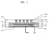
- FIG. 1 is a cross-sectional view of a reflective unit according to an embodiment of the present invention.
- the reflective unit includes an electroactive polymer layer 107 which becomes strained when a voltage is applied thereto, a light reflecting unit 115 which deforms according to the strain of the electroactive polymer layer 107 and reflecting external light, and a light blocking unit 118 disposed over the light reflecting unit 115 which prevents external light from being reflected by the light reflecting unit 115 and absorbs light reflected off the light reflecting unit 115.
- the light reflecting unit 115 for reflecting external light includes reflecting cells 115a disposed on the electroactive polymer layer 107 and spaced apart from one another, and a distance between each of the reflecting cells 115a changes according to the strain of the electroactive polymer layer 107.
- the reflective unit controls the reflectance of light by controlling a voltage applied to the electroactive polymer layer 107.
- the electroactive polymer layer 107 is strained when a voltage is applied thereto.
- a first electrode 105 and a second electrode 110 apply a voltage to the electroactive polymer layer 107.
- a stress is applied to the electroactive polymer layer 107 due to an electric field generated between the first electrode 105 and the second electrode 110, and thus the electroactive polymer 107 is strained due to the stress.
- the first electrode 105 may be disposed under the electroactive polymer layer 107 and the second electrode 110 may be disposed over the electroactive polymer layer 107.
- Each of the first electrode 105 and the second electrode 110 may be formed of a flexible material so that they can be deformed when the electroactive polymer layer 107 is strained.
- the properties of an electroactive polymer are disclosed in R. Pelrine, et. al., Science. 287, 836 (2000 ).
- the degree of strain of the electroactive polymer layer 107 varies depending on what kind of polymer is used.
- the strain amounts for a variety of polymers are shown in Table 1. Table 1.
- Circular and linear strain test results Material Prestrain (x,y)(%) Actuated relative area strain (%) Actuated relative area strain (%) Field strength (MV/m) Effective compressive stress (MPa) Estimated 1/2e (MJ/m 3 ) Circular strain HS3 silicone (68,68) 48 93 110 0.3 0.098 (14,14) 41 69 72 0.13 0.034 CF 19-2186 silicon (45,45) 39 64 350 3.0 0.75 (15,15) 25 33 160 0.6 0.091 VHB 4910 acrylic (300,300) 61 158 412 7.2 3.4 (15,15) 29 40 55 0.13 0.022 Linear strain HS3 (280,0) 54 117 128 0.4 0.16 CF 19-2186 (100,0) 39 63 181 0.8 0.2 VHB 4910 (540,75) 68 215 239 2.4 1.36
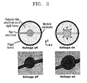
- FIG. 2 illustrates an electroactive polymer before and after a voltage is applied to the electroactive polymer.
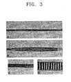
- FIG. 3 illustrates a cross section of an electroactive polymer when a linear prestrain is first applied and then a voltage is applied. Referring to FIG. 3 , the cross sectional area of the electroactive polymer is increased from A to B, and from C to D.
- the light reflecting unit 115 which is disposed on the electroactive polymer layer 107, is deformed when the electroactive polymer layer 107 is strained such that a distance between the reflecting cells 115a is changed.
- the reflecting cells 115 may be reflecting micro mirrors.
- the light reflecting unit 115 may be disposed on the second electrode 110.
- the light reflecting layer 115 may be disposed on the support layer 113.
- the support layer 113 may be formed of an electroactive polymer.
- the light blocking unit 118 may include a plurality of blocking cells 118a corresponding to the reflecting cells 115a of the light reflecting unit 115.
- the blocking cells 118a are arranged at predetermined intervals to be spaced apart from one another and face the reflecting cells 115a such that the blocking cells 118 can prevent external light from being reflected by the light reflecting unit 115 when no voltage is applied to the electroactive polymer layer 107.
- the blocking cells 118a absorb light and prevent light from passing therethrough.
- the light blocking unit 118 may be spaced apart from the light reflecting unit 115, and a space between the light reflecting unit 115 and the light blocking unit 118 may be filled with a low reflective medium 120.
- the low reflective medium 120 may be formed of an index matching material.
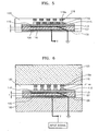
- FIG. 4A illustrates the state where the reflecting cells 115a and the blocking cells 118a are aligned with each other when no voltage is applied to the electroactive polymer layer 107. That is, the centrelines of the reflecting cells 115a and the blocking cells 118a coincide with each other. In this state, part of external light L is absorbed by the blocking cells 118a, and the remaining part of the external light L which passes between the blocking cells 118a, is reflected by the reflecting cells 115a, and then is absorbed by the blocking cells 118a, thereby displaying black.
- the blocking cells 118a may be formed of a material that can absorb light, and the reflecting cells 115a and the blocking cells 118a may have the same width.
- FIG. 4B illustrates the state where the electroactive polymer layer 107 strained and the reflecting cells 115a are accordingly extended when a first voltage V1 is applied to the electroactive polymer layer 107. Since the light reflecting unit 115 is deformed whereas the light blocking unit 118 is not deformed when the first voltage V1 is applied to the electroactive polymer layer 107, there is a positional difference between the light reflecting unit 115 and the light blocking unit 118. Therefore, the centrelines of the light reflecting cells 115a and the blocking cells 118a no longer coincide with each other. In this state, part of the external light L which passes between the blocking cells 118a, is reflected by the reflecting cells 115a, and is reflected by the reflective unit.
- the distance d between the reflecting cells 115a can be controlled by changing the voltage V applied to the electroactive polymer layer 107 and the distance t between the first electrode 105 and the second electrode 110. As the voltage V increases, the distance d between the reflecting cells 115a increases, and as the distance t between the first electrode 105 and the second electrode 110 increases, the distance d between the reflecting cells 115a decreases. If the electroactive polymer layer 107 is thick, the electroactive polymer layer 107 is strained only when a high voltage is applied. Accordingly, the electroactive polymer layer 107 should have a thickness ranging from 0.001 to 100 ⁇ m.
- FIG. 4C illustrates the state where the electroactive polymer layer 107 strained and the reflecting cells 115a are accordingly extended when a second voltage V2 greater than the first voltage V1 is applied to the electro active polymer layer 107.
- the degree of strain of the electroactive polymer layer 107 when the second voltage V2 is applied to the electroactive polymer layer 107 is greater than the degree of strain of the electroactive polymer layer 107 when the first voltage V1 is applied to the electroactive polymer layer 107.
- the degree of deformation of the reflecting cells 115a when the second voltage V2 is applied to the electroactive polymer layer 107 is greater than the degree of deformation of the reflecting cells 115a when the first voltage V1 is applied to the electroactive polymer layer.
- FIG. 5 is a cross-sectional view illustrating a modification of the reflective unit of FIG. 1 .
- the reflective unit of FIG. 5 is different from the reflective unit of FIG. 1 in that sub-blocking cells 116 are disposed between the reflecting cells 115a.
- the sub-blocking cells 116 may be disposed to prevent external light from passing between the blocking cells 118a from being reflected between the reflecting cells 115 when black is to be displayed.
- a flexible display according to the present invention employs the reflecting unit to display gradation.
- the flexible display adjusts the reflectance of light in order to display gradation using an electroactive polymer that is strained when a voltage is applied thereto.
- the flexible display includes a plurality of pixels, and the plurality of pixels emit different light according to input signals.
- the flexible display creates an image by reflecting external light, such as sunlight or ambient light.
- FIG. 6 is a cross-sectional view of a pixel of a flexible display according to an embodiment of the present invention.
- the pixel includes a first substrate 100, an electroactive polymer layer 107 disposed on the first substrate 100, a light reflecting unit 115 disposed on the electroactive polymer layer 107, and a light blocking unit 118 disposed over the light reflecting unit 115.
- An insulating layer 103 may be disposed between the first substrate 100 and the electroactive polymer layer 107.
- a second substrate 123 may be disposed over the electroactive polymer layer 107.
- the second substrate 123 may be formed of a transparent material, such as polyethylene terephthalate (PET) or glass, through which light can be transmitted.
- PET polyethylene terephthalate
- gradation of each pixel can be displayed by controlling a voltage applied to the electroactive polymer layer 107 to control the amount of light reflected by the light reflecting unit 115. That is, desired gradation for each pixel can be displayed by controlling a misalignment between the light reflecting unit 115 and the light blocking unit 118.
- FIG. 7 is a cross-sectional view of a modification of the flexible display of FIG. 6 .
- the flexible display of FIG. 7 is different from the flexible display of FIG. 6 in that a first anti-reflection layer 121 is disposed under the second substrate 123 and a second anti-reflection layer 125 is disposed over the second substrate 123.
- the first anti-reflection layer 121 and the second anti-reflection layer 125 prevent external light from being reflected before reaching the light reflecting unit 115 in order to increase the amount of light incident on the light reflecting unit 115.
- the electroactive polymer layer 107 has a rapid response to an input signal, there is no difficulty in producing a moving picture. Since the degree of strain of the electroactive polymer can be easily adjusted according to a voltage applied thereto and the reflectance of light can be adjusted according to the degree of strain due to the voltage, contrast can be improved.
- the reflective unit and the flexible display employing the reflective unit according to the present invention displays gradation and an image by controlling the reflectance of external light according to the strain of the electroactive polymer layer. Since the light reflecting unit, which is disposed on the electroactive polymer layer, is misaligned with the light blocking layer, which is disposed to face the light reflecting unit, when the electroactive polymer layer is strained, contrast can be improved by controlling the reflectance of light by controlling the amount of strain. Also, since the electroactive polymer layer has a short response time, a moving picture can be easily produced.
Landscapes
- Physics & Mathematics (AREA)
- General Physics & Mathematics (AREA)
- Optics & Photonics (AREA)
- Electrochromic Elements, Electrophoresis, Or Variable Reflection Or Absorption Elements (AREA)
- Mechanical Light Control Or Optical Switches (AREA)
- Surface Treatment Of Optical Elements (AREA)
Applications Claiming Priority (1)
| Application Number | Priority Date | Filing Date | Title |
|---|---|---|---|
| KR1020070050264A KR100888480B1 (ko) | 2007-05-23 | 2007-05-23 | 전기 활성 고분자를 이용한 반사 유닛 및 플렉서블디스플레이 |
Publications (2)
| Publication Number | Publication Date |
|---|---|
| EP1995622A1 EP1995622A1 (en) | 2008-11-26 |
| EP1995622B1 true EP1995622B1 (en) | 2011-03-30 |
Family
ID=39577612
Family Applications (1)
| Application Number | Title | Priority Date | Filing Date |
|---|---|---|---|
| EP08151633A Active EP1995622B1 (en) | 2007-05-23 | 2008-02-19 | Reflective unit using electroactive polymer and flexible display employing the reflective unit |
Country Status (5)
| Country | Link |
|---|---|
| US (1) | US7660025B2 (ko) |
| EP (1) | EP1995622B1 (ko) |
| JP (1) | JP5240989B2 (ko) |
| KR (1) | KR100888480B1 (ko) |
| DE (1) | DE602008005807D1 (ko) |
Families Citing this family (17)
| Publication number | Priority date | Publication date | Assignee | Title |
|---|---|---|---|---|
| ATE522838T1 (de) * | 2006-06-01 | 2011-09-15 | Light Resonance Technologies Llc | Lichtfilter/-modulator und array von filtern/modulatoren |
| WO2010078662A1 (en) | 2009-01-09 | 2010-07-15 | Optotune Ag | Electroactive optical device |
| US8686951B2 (en) * | 2009-03-18 | 2014-04-01 | HJ Laboratories, LLC | Providing an elevated and texturized display in an electronic device |
| KR101067661B1 (ko) * | 2009-04-14 | 2011-09-27 | 한국과학기술원 | 이온에 의해 작동되는 전기 활성 폴리머를 이용한 유연 디스플레이 형상변형장치 및 그 방법 |
| US20110199342A1 (en) | 2010-02-16 | 2011-08-18 | Harry Vartanian | Apparatus and method for providing elevated, indented or texturized sensations to an object near a display device or input detection using ultrasound |
| EP2239600A1 (en) | 2010-06-02 | 2010-10-13 | Optotune AG | Adjustable optical lens |
| EP2612065B1 (en) | 2010-09-02 | 2017-05-17 | Optotune AG | Illumination source with variable divergence |
| BR112013005408A8 (pt) * | 2010-09-09 | 2018-04-03 | Koninklijke Philips Nv | Acionador e método de fabricação do acionador |
| EP2450734A1 (en) | 2010-11-03 | 2012-05-09 | Sony Ericsson Mobile Communications AB | Optical filter arrangement and a method for adjustment thereof |
| EP2912502B1 (en) * | 2012-07-20 | 2016-04-27 | Koninklijke Philips N.V. | Variable diffuser |
| KR101983858B1 (ko) | 2012-10-25 | 2019-05-30 | 삼성디스플레이 주식회사 | 층 사이의 간격을 조절할 수 있는 디스플레이 장치 |
| KR102447739B1 (ko) * | 2014-12-09 | 2022-09-27 | 엘지디스플레이 주식회사 | 가변 소자 및 가변 소자 제조 방법 |
| EP3032597B1 (en) * | 2014-12-09 | 2019-02-27 | LG Display Co., Ltd. | Transformable device and method of manufacturing the same |
| US9960375B2 (en) * | 2015-08-31 | 2018-05-01 | Lg Display Co., Ltd. | Organic light-emitting display device |
| JP6826107B2 (ja) * | 2015-09-21 | 2021-02-03 | コーニンクレッカ フィリップス エヌ ヴェKoninklijke Philips N.V. | ユーザの生理学的パラメータを測定するためのウェアラブルデバイス及び測定方法 |
| CN107240600B (zh) * | 2017-06-26 | 2019-10-18 | 京东方科技集团股份有限公司 | 一种柔性显示装置 |
| EP3650986A1 (en) * | 2018-11-08 | 2020-05-13 | Robert Bosch GmbH | Haptic feedback screen and flat screen comprising a haptic feedback screen |
Family Cites Families (10)
| Publication number | Priority date | Publication date | Assignee | Title |
|---|---|---|---|---|
| JPS59116615A (ja) | 1982-12-22 | 1984-07-05 | Seikosha Co Ltd | カラー表示装置 |
| JPH10186249A (ja) * | 1996-12-24 | 1998-07-14 | Casio Comput Co Ltd | 表示装置 |
| WO2001077255A2 (en) | 2000-04-05 | 2001-10-18 | California Institute Of Technology | Polymers for control of orientation and stability of liquid crystals |
| US7003187B2 (en) * | 2000-08-07 | 2006-02-21 | Rosemount Inc. | Optical switch with moveable holographic optical element |
| JP2003021848A (ja) | 2001-07-06 | 2003-01-24 | Sony Corp | 表示素子 |
| JP2003091025A (ja) * | 2001-09-18 | 2003-03-28 | Ricoh Co Ltd | 表示素子およびその製造方法 |
| US6951397B1 (en) * | 2002-03-19 | 2005-10-04 | Lockheed Martin Corporation | Composite ultra-light weight active mirror for space applications |
| US7061661B2 (en) * | 2003-11-06 | 2006-06-13 | Eastman Kodak Company | Electromechanical display panel incorporating a porous movable film |
| FR2875607B1 (fr) * | 2004-09-20 | 2006-11-24 | Cit Alcatel | Miroir a deformation locale par variation d'epaisseur d'un materiau electro-actif controlee par effet electrique |
| CN101228093B (zh) * | 2005-07-22 | 2012-11-28 | 高通Mems科技公司 | 具有支撑结构的mems装置及其制造方法 |
-
2007
- 2007-05-23 KR KR1020070050264A patent/KR100888480B1/ko active IP Right Grant
- 2007-12-13 US US11/955,745 patent/US7660025B2/en active Active
-
2008
- 2008-02-19 DE DE602008005807T patent/DE602008005807D1/de active Active
- 2008-02-19 EP EP08151633A patent/EP1995622B1/en active Active
- 2008-02-20 JP JP2008038893A patent/JP5240989B2/ja active Active
Also Published As
| Publication number | Publication date |
|---|---|
| JP2008292979A (ja) | 2008-12-04 |
| US20080291521A1 (en) | 2008-11-27 |
| EP1995622A1 (en) | 2008-11-26 |
| JP5240989B2 (ja) | 2013-07-17 |
| DE602008005807D1 (de) | 2011-05-12 |
| US7660025B2 (en) | 2010-02-09 |
| KR20080103231A (ko) | 2008-11-27 |
| KR100888480B1 (ko) | 2009-03-12 |
Similar Documents
| Publication | Publication Date | Title |
|---|---|---|
| EP1995622B1 (en) | Reflective unit using electroactive polymer and flexible display employing the reflective unit | |
| CN108364602B (zh) | 柔性显示面板、其制作方法和其光学补偿方法 | |
| US7236663B2 (en) | Display element and display device using the same | |
| US6570324B1 (en) | Image display device with array of lens-lets | |
| EP0528397A2 (en) | Ferroelectric liquid crystal panel and method of manufacturing same | |
| US9757923B2 (en) | Display device and method of manufacturing the same | |
| TWI433071B (zh) | 三維曲面顯示裝置、其製造方法及可塑性顯示面板 | |
| US8294972B2 (en) | Display devices | |
| CN108445687A (zh) | 一种阵列基板、显示面板和液晶显示装置 | |
| WO2004049050A1 (en) | Method of manufacturing a curved display | |
| US20070040972A1 (en) | Flexible display device | |
| US8514480B2 (en) | Display apparatus using dielectrophoresis and method of manufacturing the display apparatus | |
| US8203778B2 (en) | Electrophoretic display device and method for manufacturing same | |
| CN107507588A (zh) | 显示面板的驱动电路及驱动方法 | |
| US11175544B2 (en) | Stretchable electrooptical and mechanooptical devices comprising a liquid crystal cell disposed between first and second ionic conducting gel layers | |
| US8284372B2 (en) | Liquid crystal display panel and method for manufacturing same, and liquid crystal display device | |
| CN108139796B (zh) | 显示面板、显示装置及其制造方法 | |
| CN109073951B (zh) | 可伸展的电光显示器 | |
| WO2007082114A2 (en) | Addressable trace structures and devices | |
| US8040593B2 (en) | Transflective display apparatus using dielectrophoresis and method of manufacturing the transflective display apparatus | |
| US20210278740A1 (en) | Optical beam processing device | |
| US20100188317A1 (en) | Reflective type display apparatus using dielectrophoresis and method of manufacturing the reflective type display apparatus | |
| CN108663841B (zh) | 液晶显示装置及其制作方法 | |
| US7408711B2 (en) | Polarizing plate, method for manufacturing the same, and liquid crystal display panel having the same | |
| US7508477B2 (en) | Liquid crystal display panel for multi-display |
Legal Events
| Date | Code | Title | Description |
|---|---|---|---|
| PUAI | Public reference made under article 153(3) epc to a published international application that has entered the european phase |
Free format text: ORIGINAL CODE: 0009012 |
|
| AK | Designated contracting states |
Kind code of ref document: A1 Designated state(s): AT BE BG CH CY CZ DE DK EE ES FI FR GB GR HR HU IE IS IT LI LT LU LV MC MT NL NO PL PT RO SE SI SK TR |
|
| AX | Request for extension of the european patent |
Extension state: AL BA MK RS |
|
| 17P | Request for examination filed |
Effective date: 20090121 |
|
| 17Q | First examination report despatched |
Effective date: 20090226 |
|
| AKX | Designation fees paid |
Designated state(s): DE FR GB NL |
|
| GRAP | Despatch of communication of intention to grant a patent |
Free format text: ORIGINAL CODE: EPIDOSNIGR1 |
|
| GRAS | Grant fee paid |
Free format text: ORIGINAL CODE: EPIDOSNIGR3 |
|
| GRAA | (expected) grant |
Free format text: ORIGINAL CODE: 0009210 |
|
| AK | Designated contracting states |
Kind code of ref document: B1 Designated state(s): DE FR GB NL |
|
| REG | Reference to a national code |
Ref country code: GB Ref legal event code: FG4D |
|
| REF | Corresponds to: |
Ref document number: 602008005807 Country of ref document: DE Date of ref document: 20110512 Kind code of ref document: P |
|
| REG | Reference to a national code |
Ref country code: DE Ref legal event code: R096 Ref document number: 602008005807 Country of ref document: DE Effective date: 20110512 |
|
| REG | Reference to a national code |
Ref country code: NL Ref legal event code: T3 |
|
| PLBE | No opposition filed within time limit |
Free format text: ORIGINAL CODE: 0009261 |
|
| STAA | Information on the status of an ep patent application or granted ep patent |
Free format text: STATUS: NO OPPOSITION FILED WITHIN TIME LIMIT |
|
| 26N | No opposition filed |
Effective date: 20120102 |
|
| REG | Reference to a national code |
Ref country code: DE Ref legal event code: R097 Ref document number: 602008005807 Country of ref document: DE Effective date: 20120102 |
|
| REG | Reference to a national code |
Ref country code: FR Ref legal event code: PLFP Year of fee payment: 9 |
|
| REG | Reference to a national code |
Ref country code: FR Ref legal event code: PLFP Year of fee payment: 10 |
|
| REG | Reference to a national code |
Ref country code: FR Ref legal event code: PLFP Year of fee payment: 11 |
|
| REG | Reference to a national code |
Ref country code: GB Ref legal event code: 732E Free format text: REGISTERED BETWEEN 20200319 AND 20200325 |
|
| REG | Reference to a national code |
Ref country code: DE Ref legal event code: R082 Ref document number: 602008005807 Country of ref document: DE Representative=s name: DR. WEITZEL & PARTNER PATENT- UND RECHTSANWAEL, DE Ref country code: DE Ref legal event code: R081 Ref document number: 602008005807 Country of ref document: DE Owner name: SAMSUNG DISPLAY CO., LTD., YONGIN-SI, KR Free format text: FORMER OWNER: SAMSUNG ELECTRONICS CO., LTD., SUWON-SI, GYEONGGI-DO, KR Ref country code: DE Ref legal event code: R081 Ref document number: 602008005807 Country of ref document: DE Owner name: HYDIS TECHNOLOGIES CO., LTD., KR Free format text: FORMER OWNER: SAMSUNG ELECTRONICS CO., LTD., SUWON-SI, GYEONGGI-DO, KR |
|
| REG | Reference to a national code |
Ref country code: NL Ref legal event code: PD Owner name: SAMSUNG DISPLAY CO., LTD; KR Free format text: DETAILS ASSIGNMENT: CHANGE OF OWNER(S), ASSIGNMENT; FORMER OWNER NAME: SAMSUNG ELECTRONICS CO., LTD Effective date: 20200706 |
|
| REG | Reference to a national code |
Ref country code: GB Ref legal event code: 732E Free format text: REGISTERED BETWEEN 20210107 AND 20210113 |
|
| REG | Reference to a national code |
Ref country code: NL Ref legal event code: PD Owner name: HYDIS TECHNOLOGIES CO., LTD.; KR Free format text: DETAILS ASSIGNMENT: CHANGE OF OWNER(S), ASSIGNMENT; FORMER OWNER NAME: SAMSUNG ELECTRONICS CO., LTD Effective date: 20210209 |
|
| REG | Reference to a national code |
Ref country code: DE Ref legal event code: R082 Ref document number: 602008005807 Country of ref document: DE Representative=s name: DR. WEITZEL & PARTNER PATENT- UND RECHTSANWAEL, DE Ref country code: DE Ref legal event code: R081 Ref document number: 602008005807 Country of ref document: DE Owner name: HYDIS TECHNOLOGIES CO., LTD., KR Free format text: FORMER OWNER: SAMSUNG DISPLAY CO., LTD., YONGIN-SI, GYEONGGI-DO, KR |
|
| PGFP | Annual fee paid to national office [announced via postgrant information from national office to epo] |
Ref country code: FR Payment date: 20230119 Year of fee payment: 16 |
|
| P01 | Opt-out of the competence of the unified patent court (upc) registered |
Effective date: 20230515 |
|
| PGFP | Annual fee paid to national office [announced via postgrant information from national office to epo] |
Ref country code: NL Payment date: 20240123 Year of fee payment: 17 |
|
| PGFP | Annual fee paid to national office [announced via postgrant information from national office to epo] |
Ref country code: DE Payment date: 20240122 Year of fee payment: 17 Ref country code: GB Payment date: 20240122 Year of fee payment: 17 |