EP1992720A1 - Etchant and method for fabricating electric device including thin film transistor using the same - Google Patents
Etchant and method for fabricating electric device including thin film transistor using the same Download PDFInfo
- Publication number
- EP1992720A1 EP1992720A1 EP08251301A EP08251301A EP1992720A1 EP 1992720 A1 EP1992720 A1 EP 1992720A1 EP 08251301 A EP08251301 A EP 08251301A EP 08251301 A EP08251301 A EP 08251301A EP 1992720 A1 EP1992720 A1 EP 1992720A1
- Authority
- EP
- European Patent Office
- Prior art keywords
- etchant
- layer
- etching
- thin film
- film transistor
- Prior art date
- Legal status (The legal status is an assumption and is not a legal conclusion. Google has not performed a legal analysis and makes no representation as to the accuracy of the status listed.)
- Granted
Links
Images







Classifications
-
- C—CHEMISTRY; METALLURGY
- C23—COATING METALLIC MATERIAL; COATING MATERIAL WITH METALLIC MATERIAL; CHEMICAL SURFACE TREATMENT; DIFFUSION TREATMENT OF METALLIC MATERIAL; COATING BY VACUUM EVAPORATION, BY SPUTTERING, BY ION IMPLANTATION OR BY CHEMICAL VAPOUR DEPOSITION, IN GENERAL; INHIBITING CORROSION OF METALLIC MATERIAL OR INCRUSTATION IN GENERAL
- C23F—NON-MECHANICAL REMOVAL OF METALLIC MATERIAL FROM SURFACE; INHIBITING CORROSION OF METALLIC MATERIAL OR INCRUSTATION IN GENERAL; MULTI-STEP PROCESSES FOR SURFACE TREATMENT OF METALLIC MATERIAL INVOLVING AT LEAST ONE PROCESS PROVIDED FOR IN CLASS C23 AND AT LEAST ONE PROCESS COVERED BY SUBCLASS C21D OR C22F OR CLASS C25
- C23F1/00—Etching metallic material by chemical means
- C23F1/10—Etching compositions
- C23F1/14—Aqueous compositions
- C23F1/16—Acidic compositions
- C23F1/18—Acidic compositions for etching copper or alloys thereof
-
- C—CHEMISTRY; METALLURGY
- C23—COATING METALLIC MATERIAL; COATING MATERIAL WITH METALLIC MATERIAL; CHEMICAL SURFACE TREATMENT; DIFFUSION TREATMENT OF METALLIC MATERIAL; COATING BY VACUUM EVAPORATION, BY SPUTTERING, BY ION IMPLANTATION OR BY CHEMICAL VAPOUR DEPOSITION, IN GENERAL; INHIBITING CORROSION OF METALLIC MATERIAL OR INCRUSTATION IN GENERAL
- C23F—NON-MECHANICAL REMOVAL OF METALLIC MATERIAL FROM SURFACE; INHIBITING CORROSION OF METALLIC MATERIAL OR INCRUSTATION IN GENERAL; MULTI-STEP PROCESSES FOR SURFACE TREATMENT OF METALLIC MATERIAL INVOLVING AT LEAST ONE PROCESS PROVIDED FOR IN CLASS C23 AND AT LEAST ONE PROCESS COVERED BY SUBCLASS C21D OR C22F OR CLASS C25
- C23F1/00—Etching metallic material by chemical means
- C23F1/10—Etching compositions
- C23F1/14—Aqueous compositions
- C23F1/16—Acidic compositions
- C23F1/26—Acidic compositions for etching refractory metals
-
- H—ELECTRICITY
- H10—SEMICONDUCTOR DEVICES; ELECTRIC SOLID-STATE DEVICES NOT OTHERWISE PROVIDED FOR
- H10D—INORGANIC ELECTRIC SEMICONDUCTOR DEVICES
- H10D30/00—Field-effect transistors [FET]
- H10D30/01—Manufacture or treatment
- H10D30/021—Manufacture or treatment of FETs having insulated gates [IGFET]
- H10D30/031—Manufacture or treatment of FETs having insulated gates [IGFET] of thin-film transistors [TFT]
- H10D30/0312—Manufacture or treatment of FETs having insulated gates [IGFET] of thin-film transistors [TFT] characterised by the gate electrodes
- H10D30/0316—Manufacture or treatment of FETs having insulated gates [IGFET] of thin-film transistors [TFT] characterised by the gate electrodes of lateral bottom-gate TFTs comprising only a single gate
-
- H—ELECTRICITY
- H10—SEMICONDUCTOR DEVICES; ELECTRIC SOLID-STATE DEVICES NOT OTHERWISE PROVIDED FOR
- H10D—INORGANIC ELECTRIC SEMICONDUCTOR DEVICES
- H10D30/00—Field-effect transistors [FET]
- H10D30/01—Manufacture or treatment
- H10D30/021—Manufacture or treatment of FETs having insulated gates [IGFET]
- H10D30/031—Manufacture or treatment of FETs having insulated gates [IGFET] of thin-film transistors [TFT]
- H10D30/0321—Manufacture or treatment of FETs having insulated gates [IGFET] of thin-film transistors [TFT] comprising silicon, e.g. amorphous silicon or polysilicon
-
- H—ELECTRICITY
- H10—SEMICONDUCTOR DEVICES; ELECTRIC SOLID-STATE DEVICES NOT OTHERWISE PROVIDED FOR
- H10D—INORGANIC ELECTRIC SEMICONDUCTOR DEVICES
- H10D30/00—Field-effect transistors [FET]
- H10D30/60—Insulated-gate field-effect transistors [IGFET]
- H10D30/67—Thin-film transistors [TFT]
- H10D30/6729—Thin-film transistors [TFT] characterised by the electrodes
- H10D30/6737—Thin-film transistors [TFT] characterised by the electrodes characterised by the electrode materials
-
- H—ELECTRICITY
- H10—SEMICONDUCTOR DEVICES; ELECTRIC SOLID-STATE DEVICES NOT OTHERWISE PROVIDED FOR
- H10D—INORGANIC ELECTRIC SEMICONDUCTOR DEVICES
- H10D30/00—Field-effect transistors [FET]
- H10D30/60—Insulated-gate field-effect transistors [IGFET]
- H10D30/67—Thin-film transistors [TFT]
- H10D30/6729—Thin-film transistors [TFT] characterised by the electrodes
- H10D30/6737—Thin-film transistors [TFT] characterised by the electrodes characterised by the electrode materials
- H10D30/6739—Conductor-insulator-semiconductor electrodes
-
- H—ELECTRICITY
- H10—SEMICONDUCTOR DEVICES; ELECTRIC SOLID-STATE DEVICES NOT OTHERWISE PROVIDED FOR
- H10D—INORGANIC ELECTRIC SEMICONDUCTOR DEVICES
- H10D30/00—Field-effect transistors [FET]
- H10D30/60—Insulated-gate field-effect transistors [IGFET]
- H10D30/67—Thin-film transistors [TFT]
- H10D30/674—Thin-film transistors [TFT] characterised by the active materials
- H10D30/6741—Group IV materials, e.g. germanium or silicon carbide
- H10D30/6743—Silicon
-
- H—ELECTRICITY
- H10—SEMICONDUCTOR DEVICES; ELECTRIC SOLID-STATE DEVICES NOT OTHERWISE PROVIDED FOR
- H10K—ORGANIC ELECTRIC SOLID-STATE DEVICES
- H10K71/00—Manufacture or treatment specially adapted for the organic devices covered by this subclass
- H10K71/621—Providing a shape to conductive layers, e.g. patterning or selective deposition
-
- H—ELECTRICITY
- H10—SEMICONDUCTOR DEVICES; ELECTRIC SOLID-STATE DEVICES NOT OTHERWISE PROVIDED FOR
- H10P—GENERIC PROCESSES OR APPARATUS FOR THE MANUFACTURE OR TREATMENT OF DEVICES COVERED BY CLASS H10
- H10P50/00—Etching of wafers, substrates or parts of devices
- H10P50/60—Wet etching
- H10P50/66—Wet etching of conductive or resistive materials
- H10P50/663—Wet etching of conductive or resistive materials by chemical means only
- H10P50/667—Wet etching of conductive or resistive materials by chemical means only by liquid etching only
Definitions
- the present embodiments relate to an etchant and a method for fabricating an electric device including a thin film transistor using the same. More particularly, the embodiments of the present invention relate to an etchant that can provide a high quality display due to a high aperture ratio and high definition, and reduced resistor-capacitor signal delay (referred to as RC delay), and a method for fabricating an electric device including a thin film transistor using the same.
- RC delay reduced resistor-capacitor signal delay
- a thin film transistor In an active matrix liquid crystal display and an active matrix organic light emitting diode (OLED) display, a thin film transistor (TFT) is generally used as a switching device at each liquid crystal cell or each pixel.
- molybdenum (Mo) with resistivity of less than 12 ⁇ cm and aluminum (Al) with resistivity of less than 5.5 ⁇ cm are used as wire for a thin film transistor or an electrode. Since these metals have high resistivity, they tend to make it difficult to manufacture a larger liquid crystal display and OLED display with higher resolution. Copper (Cu) in contrast has a resistivity of less than 2.2 ⁇ cm, and is being researched as an alternative material for wires and electrodes.
- Copper can be applied to all of a gate electrode, a source electrode, and a drain electrode of a thin film transistor.
- a gate electrode when copper is applied to a gate electrode, it has poor adherence to a glass substrate where a thin film transistor is formed.
- a source electrode and a drain electrode when it is applied to a source electrode and a drain electrode, it may react with a silicon (Si) film that is used as a buffer. Therefore, when copper is applied to a gate electrode, a source electrode, and/or a drain electrode, it cannot be used as a single layer but is used as a copper/titanium or a copper/titanium alloy by disposing a barrier metal such as titanium (Ti) beneath it.
- a barrier metal such as titanium (Ti)
- the copper/titanium or copper/titanium alloy is treated with a photolithography process and an etching process to form a wire and an electrode.
- a copper (Cu) layer as a first gate metal layer is deposited on a substrate.
- a titanium (Ti) layer or a titanium alloy layer as a second gate metal layer is deposited on the first gate metal layer.
- the second gate metal layer is selectively patterned to form a second gate pattern
- the first gate metal layer is selectively patterned to form a first gate pattern.
- the patterning process of the first and second gate metal layers is included in an etching process.
- the first gate metal layer and the second gate metal layer are separately etched.
- an etchant as set out in Claim 1.
- Preferred features of this aspect are set out in Claims 2 to 7.
- the multi-layered film can be a double layered film such as a copper layer/titanium layer or a copper layer/titanium alloy layer, or a triple-layered film such as titanium layer/copper layer/titanium layer or a titanium alloy layer/copper layer/titanium alloy layer, on a substrate. It is therefore possible to obtain a multi-layered film having a uniform pattern profile with a high yield reducing fabrication cost.
- the thin film transistor 20 includes a gate electrode 22 connected to a gate wire 21, a semiconductor layer 24 disposed on the gate electrode 22, a source electrode 26 connected to a data wire 25 on the semiconductor layer 24, and a drain electrode 28 spaced by a predetermined interval from the source electrode 26 on the semiconductor layer 24.
- the gate electrode 22, source electrode 26, and drain electrode 28 can be made of a metallic material.
- a multi-layered film including a copper layer, and a titanium or titanium alloy layer with low resistance should be applied.
- a conventional etchant may cause critical dimension loss (CD-loss) of the copper/titanium or copper/titanium alloy layers depending on the number of etched substrates.
- the critical dimension loss (CD-loss) rate may not increase at a particular rate.
- the conventional etchant has a problem of not uniformly controlling a pattern profile of a multi-layered film including a copper layer, and a titanium or titanium alloy layer, and it also decreases the yield rate and increases fabrication cost since it needs to be frequently replaced.
- an etchant is provided to etch the multi-layered film.
- the etchant includes a fluorine ion (F - ) source; hydrogen peroxide (H 2 O 2 ); a sulfate; a phosphate; an azole-based compound; and a solvent.
- the fluorine ion source is present at a concentration of from about 0.01 wt% to about 10 wt%
- the hydrogen peroxide is present at a concentration of from about 1 wt% to about 20 wt%
- the sulfate is present at a concentration of from about 0.1 wt% to about 10 wt%
- the phosphate is present at a concentration of from about 0.1 wt% to about 10 wt%
- the azole-based compound is present at a concentration of from about 0.01 wt% to about 5 wt%
- solvent is present in a balance amount.
- titanium is easily reacted with the fluorine ions to produce titanium fluoride (TiF 4 ).
- the fluorine ion source is provided by a fluoride selected from at least one from the group consisting of ammonium fluoride (NH 4 F), ammonium hydrogen fluoride (NH 4 HF 2 ), potassium fluoride (KF), sodium fluoride (NaF), and combinations thereof as well as the above hydrogen fluoride (HF).
- the fluoride is dissociated in an aqueous solution to produce fluorine ions.
- the fluorine ion source is present at a concentration of less than 0.01wt % the etch-rate of the titanium or titanium alloy is too slow.
- the fluoride ion source is present at a concentration of more than 10 wt% then the etch rate of the titanium or titanium alloy is too fast. More preferably, the fluorine ion source is present at a concentration of from about 0.1 wt% to about 5 wt%.
- the oxygen of the hydrogen peroxide is reacted with copper to produce copper oxide (CuO), and water (H 2 O) or hydrogen gas (H 2 ).
- the copper plays a role in producing the copper oxide.
- the hydrogen peroxide is present at a concentration of from about 1 wt% to about 20 wt%. When the hydrogen peroxide is present at a concentration of less than 1 wt% the etch rate of copper is too slow. When the hydrogen peroxide is present at a concentration of more than 20 wt% to the etch-rate of the copper is too fast. More preferably, the hydrogen peroxide is present at a concentration of from about 3 wt% to about 10 wt%.
- the sulfate controls the etch-rate of the copper.
- the sulfate is used to suppress copper etching.
- the sulfate can be a compound of, for example, A 2 S0 4 , AHS0 4 , BS0 4 and combinations thereof where A is an alkali metal such as, for example, potassium (K), sodium (Na), and combinations thereof; ammonium (NH 4 + ); and combinations thereof, B is an alkaline-earth metal such as, for example, calcium (Ca), barium (Ba), and combinations thereof.
- A is an alkali metal such as, for example, potassium (K), sodium (Na), and combinations thereof; ammonium (NH 4 + ); and combinations thereof
- B is an alkaline-earth metal such as, for example, calcium (Ca), barium (Ba), and combinations thereof.
- the sulfate is selected from the group consisting of KHSO 4 , NaHSO 4 , CaSO 4 , BaSO 4 , (NH 4 )HSO 4 , and combinations thereof.
- the sulfate is present at a concentration of from about 0.1 wt
- the etch-rate of the copper may not be sufficiently suppressed.
- the sulphate is present at a concentration of more than 10 wt% the etch-rate of the copper may be too slow. More preferably, the sulfate is present at a concentration of from about 0.5 wt% to about 5 wt%.
- the phosphate controls the etch-rate of the copper. As the concentration of the phosphate increases, the etch-rate of the copper increases.
- the phosphate is selected from the group consisting of K 2 HPO 4 , Na 2 HPO 4 , CaHPO 4 , BaHPO 4 , (NH 4 )H 2 PO 4 , (NH 4 ) 3 PO 4 , and combinations thereof.
- the phosphate is present at a concentration of from about 0.1 wt% to about 10 wt%. When the phosphate is present at a concentration of less than 0.1 wt% the etch-rate of the copper may be too slow. When the phosphate is present at a concentration of more than 10 wt% the etch-rate of the copper may be too fast. More preferably, the phosphate is present at a concentration of from about 0.5 wt% to about 7 wt%.
- the azole-based compound acts as a reaction inhibitor of copper (a Cu inhibitor).
- the azole-based compound may be for example, an alkylimidazole such as methylimidazole (C 4 H 6 N 2 ) (where the alkyl is a C 1 to C 7 alkyl); pyarazole; tolyltriazole; benzotriazole; aminotetrazole; and combinations thereof.
- the azole-based compound is present at a concentration of from about 0.01 wt% to about 5 wt%. When the azole-based compound is present at a concentration of less than 0.01 wt% the copper reaction and the etch-rate of the copper cannot be sufficiently suppressed.
- the azole-based compound When the azole-based compound is present at a concentration of more than 5 wt% the copper reaction and the etch-rate of the copper may be too slow. More preferably, the azole-based compound is present at a concentration of about 0.5 wt% to about 3 wt%.
- the solvent can be purified water or de-ionized water.
- Copper ions produced by the etchant do not perform a reaction. Deterioration of etching performance with an increasing number of etched substrates can therefore be minimized. Uniform pattern profiles of the multi-layered film can therefore be obtained at a high yield, thereby reducing cost.
- the multi-layered film has a structure in which a copper layer and a titanium or titanium alloy layer are multiply layered, and can be, for example, a double layer film of copper/titanium, a double layer film of copper/titanium alloy, a triple layer film of titanium/copper/titanium, a triple layer film of titanium alloy/copper/titanium alloy, and a quintuple layer film of titanium/titanium alloy/copper/ titanium/titanium alloy.
- the titanium alloy layer is a Ti-M alloy layer (wherein M is a transition metal such as Ni, etc.).
- a method of fabricating an electric device including a thin film transistor that includes forming a multi-layered film by depositing titanium (Ti) or a titanium alloy (Ti alloy), and depositing copper (Cu); forming a selective mask by a photoresist method on the multi-layered film; and subjecting the masked multi-layered film to an etchant including fluorine ions (F - ), hydrogen peroxide (H 2 O 2 ), a sulfate, a phosphate, an azole-based compound, and a solvent to form a pattern.
- an etchant including fluorine ions (F - ), hydrogen peroxide (H 2 O 2 ), a sulfate, a phosphate, an azole-based compound, and a solvent to form a pattern.
- FIGs. 2A to 2E show a fabrication process of a substrate according to one embodiment.
- a titanium or titanium alloy layer 110 and a copper layer 120 are sequentially deposited on a substrate 100 in not less than 2 layers to form a multi-layered film.
- the titanium layer 110 improves a close-contacting property between the copper layer 120 having good conductivity and the substrate 100. Even though a gate electrode including the copper layer and titanium layer is described for better comprehension and ease of description, a gate electrode including a copper layer and a titanium alloy layer can also be applied.
- the multi-layered film is the same as above.
- the copper is formed at a thickness from about 1000 ⁇ (0.1 ⁇ m) to about 10.000 ⁇ (1 ⁇ m), preferably at a thickness from about 2000 ⁇ (0.2 ⁇ m) to about 5000 ⁇ (0.5 ⁇ m).
- the copper layer has a thickness of less than 1000 ⁇ (0.1 ⁇ m) current is not smoothly transferred and when the copper layer has a thickness of more than 10,000 ⁇ (1 ⁇ m) etching is difficult.
- the titanium or titanium alloy layer is formed at a thickness from about 10 ⁇ (0.001 ⁇ m) to about 2000 ⁇ (0.2 ⁇ m), preferably from about 40 ⁇ (0.004 ⁇ m) to about 700 ⁇ (0.07 ⁇ m).
- the titanium or titanium alloy layer has a thickness of more than 10 ⁇ (0.001 ⁇ m) uniform deposition thickness can be obtained.
- Upper layers on the titanium or titanium alloy layer are not required to be thicker than 2000 ⁇ (0.2 ⁇ m).
- a photoresist 130 is applied on the entire upper surface of the multi-layered film disposed on the substrate 100 ( FIG. 2B ), and is subjected to selective exposure and development to form a photoresist pattern 132 for a gate electrode so as to protect the multi-layered film by masking it ( FIG. 2C ).
- the masked multi-layered film is etched by the etchant ( FIG. 2D ).
- the etchant is the same as the above including the fluorine ions, hydrogen peroxide, sulfate, phosphate, and azole-based compound.
- the photoresist pattern 132 that remains on the gate electrode is removed using a stripper to form a gate electrode 142 ( FIG. 2E ).
- etching method can be applied to a source electrode and a data wire and/or a drain electrode as well as a gate electrode. Furthermore, it can be applied to all processes of pattern formation of a layer including a copper layer and a titanium or titanium alloy layer.
- the method of fabricating an electric device including a thin film transistor can etch a multi-layered film in a batch by using the etchant having the above composition and therefore process steps of a thin film transistor can be reduced, resulting in improvement of productivity and reduction of cost and inferiority rate.
- the fabricated thin film transistor can be applied to a thin film transistor-liquid crystal display (LCD) or organic light emitting diode (OLED) display.
- LCD liquid crystal display
- OLED organic light emitting diode
- a 200 ⁇ (0.02 ⁇ m) titanium layer was deposited on a glass substrate, and a 2000 ⁇ (0.2 ⁇ m) copper layer was deposited thereon to form a double-layer. Then, a photoresist was coated on the glass substrate deposited with the double-layer in order. The resulting product was selectively exposed and developed to form a mask for etching on the layers.
- An etchant was prepared by dissolving 0.3wt% of NH 4 F, 6wt% of H 2 O 2 , 3wt% of NaHSO 4 , 5wt% of (NH 4 )H 2 PO 4 , and 0.5wt% of 5-aminotetrazole in de-ionized water.
- the 200 ⁇ (0.02 ⁇ m) titanium and 2000 ⁇ (0.2 ⁇ m) copper layers were etched together by using the etchant in a spray swing method. The etching was performed at 25°C.
- a 200 ⁇ (0.02 ⁇ m) titanium layer was deposited on a glass substrate, and a 2000 ⁇ (0.2 ⁇ m) copper layer was deposited thereon to form a double-layer. Then, a photoresist was coated on the glass substrate deposited with the double-layer in order. The resulting product was selectively exposed and developed to form a mask for etching on the double-layer.
- An etchant was prepared by dissolving 0.3wt% of NH 4 F, 6wt% of H 2 O 2 , 5wt% of KHSO 4 , 3wt% of (NH 4 ) 3 PO 4 , and 0.5wt% of 5-aminotetrazole in de-ionized water.
- the double-layer was etched at one time by using the etchant in a spray swing method. The etching was performed at 25°C.
- a 500 ⁇ (0.05 ⁇ m) titanium layer, a 4000 ⁇ (0.4 ⁇ m) copper layer, and a 500 ⁇ (0.05 ⁇ m) titanium layer were sequentially deposited on a glass substrate to form a triple-layer. Then, a photoresist was coated on the glass substrate deposited with the triple-layer in order. The resulting product was selectively exposed and developed to form a mask for etching on the triple-layer.
- An etchant was prepared by dissolving 0.8wt% of HF, 10wt% of H 2 O 2 , 1wt% of KHSO 4 , 2wt% of (NH 4 )H 2 PO 4 , and 0.1wt% of 5-aminotetrazole in de-ionized water.
- the triple-layer was etched at one time by using the etchant in a spray swing method. The etching was performed at 30°C.
- a 500 ⁇ (0.05 ⁇ m) titanium layer, a 4000 ⁇ (0.4 ⁇ m) copper layer, and a 700 ⁇ (0.07 ⁇ m) titanium layer were sequentially deposited on a glass substrate to form a triple-layer. Then, a photoresist was coated on the glass substrate deposited with the triple-layer in order. The resulting product was selectively exposed and developed to form a mask for etching on the triple-layer.
- An etchant was prepared by dissolving 0.8wt% of HF, 10wt% of H 2 O 2 , 1wt% of KHSO 4 , 2wt% of (NH 4 )H 2 PO 4 , and 0.1wt% of 5-aminotetrazole in de-ionized water.
- the triple-layer was etched at one time by using the etchant in a spray swing method. The etching was performed at 30°C.
- a 500 ⁇ (0.05 ⁇ m) titanium layer, a 40 ⁇ (0.004 ⁇ m) Ti-Ni alloy layer, a 4000 ⁇ (0.4 ⁇ m) copper layer, a 40 ⁇ (0.004 ⁇ m) Ti-Ni alloy layer, and a 700 ⁇ (0.07 ⁇ m) titanium layer were sequentially deposited on a glass substrate to form a quintuple-layer. Then, a photoresist was coated on the glass substrate deposited with the quintuple-layer in order. The resulting product was selectively exposed and developed to form a mask for etching on the quintuple-layer.
- An etchant was prepared by dissolving 1wt% of HF, 10wt% of H 2 O 2 , 1wt% of KHSO 4 , 2wt% of (NH 4 )H 2 PO 4 , 1wt% of NH 4 HF 2 and 0.1wt% of 5-aminotetrazole in de-ionized water.
- the quintuple-layer was etched at one time by using the etchant in a spray swing method. The etching was performed at 30°C.
- a 500 ⁇ (0.05 ⁇ m) titanium layer, a 4000 ⁇ (0.04 ⁇ m) copper layer, and a 500 ⁇ (0.05 ⁇ m) titanium layer were sequentially deposited on a glass substrate to form a triple-layer. Then, a photoresist was coated on the glass substrate deposited with the triple-layer in order. The resulting product was selectively exposed and developed to form a mask for etching the triple-layer.
- An etchant was prepared by dissolving HF, H 2 O 2 , KHSO 4 , (NH 4 )H 2 PO 4 , and 5-aminotetrazole in an amount according to the following Table 1 in de-ionized water.
- the triple-layer was etched at one time by using the etchant in a spray swing method. The etching was performed at 30°C.
- the triple-layer was etched with the method as in Example 6, except using an etchant that was prepared by dissolving 1wt% of HF, 6wt% of H 2 O 2 , 1wt% of (NH 4 )H 2 PO 4 , and 0.1wt% of 5-aminotetrazole in de-ionized water as disclosed in Table 1, in a spray swing method.
- the etching was performed at 30°C.
- Example 7 1 6 2 1 0.1
- Example 8 1 6 5 1 0.1
- etching results of the multi-layered film of etchants according to Examples 1 to 5 such as etching time, degree of tapering, loss of critical dimension, edge sharpness, and change depending on time are provided in the following Table 2.
- the degree of tapering was determined by measuring the angle and length of the slope of copper and titanium layers with a field emission scanning electron microscope (FE-SEM).
- CD-loss The critical dimension loss
- edge sharpness was determined by measuring the length of a tail formed when both edges of titanium and copper layers were dragged on the bottom, and "change depending on time” indicates the number of substrate sheets that can maintain an etching time measured by an end point detection system (EPD system) within ⁇ 10%, when several sheets of substrates are etched with the same etchant.
- EPD system end point detection system
- the tapering degree of the substrates of Examples 1 and 2 all had an angle of 45° with a length of 0.25 ⁇ m.
- Examples 1 and 2 showed a tail height of less than 100 ⁇ (0.01 ⁇ m), and the titanium and copper layers had a length of less than 0.1 ⁇ m.
- the pattern profiles of the multi-layered film etched by using the etchant according to Examples 1 to 5 was determined by measuring with a field emission scanning electron microscope (FE-SEM). The results are provided in FIGs. 3 to 8 .
- FIG. 3A is a photograph of pattern profiles of the photoresist when over-etching with respect to time by 30% according to Example 1 of the present embodiments
- FIG. 3B is a photograph of a Cu/Ti layer when over-etching with respect to time by 30% according to Example 1 of the present embodiments
- FIG. 3C is a cross-sectional views of a Cu/Ti layer when over-etching with respect to time by 30% according to Example 1 of the present embodiments.
- FIG. 4A is a photograph of pattern profiles of the photoresist when over-etching with respect to time by 60% according to Example 1 of the present embodiments
- FIG. 4B is a photograph of a Cu/Ti layer when over-etching with respect to time by 60% according to Example 1 of the present embodiments
- FIG. 4C is a cross-sectional views of a Cu/Ti layer when over-etching with respect to time by 60% according to Example 1 of the present embodiments.
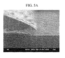
- FIG. 5A is a photograph of pattern profiles of the photoresist when etching for 60 seconds according to Example 2 of the present embodiments
- FIG. 5B is a photograph of pattern profiles of the photoresist when etching for 70 seconds according to Example 2 of the present embodiments.
- FIG. 6A is a photograph of pattern profiles of the photoresist when over-etching with respect to time by 43% according to Example 3 of the present embodiments
- FIG. 6B is a photograph of a Cu/Ti layer when over-etching with respect to time by 43% according to Example 3 of the present embodiments
- FIG. 6C is a cross-sectional views of a Cu/Ti layer when over-etching with respect to time by 43% according to Example 3 of the present embodiments.
- FIG. 7A is a photograph of pattern profiles of the photoresist when over-etching with respect to time by 60% according to Example 4 of the present embodiments
- FIG. 7B is a photograph of a Cu/Ti layer when over-etching with respect to time by 60% according to Example 4 of the present embodiments
- FIG. 7C is a cross-sectional views of a Cu/Ti layer when over-etching with respect to time by 60% according to Example 4 of the present embodiments.
- FIG. 8A is a photograph of pattern profiles of the photoresist when over-etching with respect to time by 40% according to Example 5 of the present embodiments
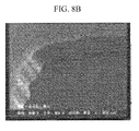
- FIG. 8B is a photograph of a Cu/Ti layer when over-etching with respect to time by 40% according to Example 5 of the present embodiments
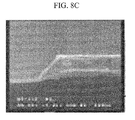
- FIG. 8C is a cross-sectional views of Cu/Ti layer when over-etching with respect to time by 60% according to Example 1 of the present embodiments.
- Examples 1 to 5 were 60% over-etched, they had pattern width decrease of less than 0.5 ⁇ m; that is to say, a bigger process margin vs. etching time.
- FIG. 9 is a graph of critical dimension loss when over-etching in Example 3 of the present embodiments
- FIG. 10 is a graph of critical dimension loss when over-etching in Example 4 of the present embodiments. As show in FIGs. 9 and 10 , the critical dimension loss when over-etching was small in Examples 3 and 4.
- the etchants including a sulfate in Examples 6 to 8 have an equal etching effect of CD-Loss compared with that of the Comparative Example 1.
- the etching time was shorter than that of Comparative Example 1. Also, as the content of the sulfate in the etchant increases, etching time decreases.
- Example 1 The etching process in Example 1 was repeated while continuously supplying the same kind of substrate.
- the etching time depending on the number of etched substrates according to Example 1 was measured, and the results are provided in FIG. 11 .
- FIG. 11 is a graph showing etching time depending on the number of etched substrates according to Example 1 of the present embodiments.
- the etchant of Example 1 was able to etch more than 1000 sheets of substrates by reusing the same etchant. Even when more than 1000 sheets of substrates deposited with a 2000 ⁇ (0.2 ⁇ m) copper layer and a 200 ⁇ (0.02 ⁇ m) titanium layer were etched, the etchant can still be used, securing a longer replacement period.
- FIG. 12 is a graph showing etching time depending on the number of etched substrates according to Example 2 of the present embodiments.
- Example 2 of the present embodiments when an etchant according to Example 2 of the present embodiments was used to etch a 5000 ⁇ (0.5 ⁇ m) copper layer, it maintained etching performance for more than 600 sheets. Based on this result, it can etch more than 1500 sheets when it is used to etch a 2000 ⁇ (0.2 ⁇ m) copper layer, which is 2.5 times that of the 5000 ⁇ (0.5 ⁇ m) copper layer.
- the present embodiments can solve unstable etching performance of copper and titanium layers as the number of etched substrates increases.
- an etchant and a method of fabricating an electric device with a thin film transistor can have an effect on prolonging use time of an etchant for etching a multi-layered film having a structure in which a copper layer and a titanium or titanium alloy layer are multiply layered, in a batch, thereby increasing yield rate by improving a pattern profile, and decreasing fabrication cost by maintaining uniform etching performance, when it is repeatedly used to etch sheets of substrates and thereby postponing its replacement period.
- the etchant and the method of fabricating an electric device with a thin film transistor according to the present embodiments can simplify the application of copper with low resistance to an electronic device and thereby the electronic device can have improved characteristics such as high-aperture ratio, high-definition, and the like, and can also have reduced register-capacitor signal delay. Accordingly, it can be manufactured to be large-sized and have high quality.
Landscapes
- Chemical & Material Sciences (AREA)
- Engineering & Computer Science (AREA)
- Chemical Kinetics & Catalysis (AREA)
- General Chemical & Material Sciences (AREA)
- Materials Engineering (AREA)
- Mechanical Engineering (AREA)
- Metallurgy (AREA)
- Organic Chemistry (AREA)
- Manufacturing & Machinery (AREA)
- Weting (AREA)
- ing And Chemical Polishing (AREA)
Abstract
Description
- The present embodiments relate to an etchant and a method for fabricating an electric device including a thin film transistor using the same. More particularly, the embodiments of the present invention relate to an etchant that can provide a high quality display due to a high aperture ratio and high definition, and reduced resistor-capacitor signal delay (referred to as RC delay), and a method for fabricating an electric device including a thin film transistor using the same.
- In an active matrix liquid crystal display and an active matrix organic light emitting diode (OLED) display, a thin film transistor (TFT) is generally used as a switching device at each liquid crystal cell or each pixel.
- Recently, there has been a tendency to increase the size of liquid crystal displays and organic light emitting diode (OLED) displays. As a consequence there is a greater requirement for higher resolution. Larger liquid crystal displays and OLED displays with higher resolution require reduced RC delay. The reduced RC delay can be accomplished by minimizing the resistance of wires.
- In general, molybdenum (Mo) with resistivity of less than 12µΩcm and aluminum (Al) with resistivity of less than 5.5µΩcm are used as wire for a thin film transistor or an electrode. Since these metals have high resistivity, they tend to make it difficult to manufacture a larger liquid crystal display and OLED display with higher resolution. Copper (Cu) in contrast has a resistivity of less than 2.2µΩcm, and is being researched as an alternative material for wires and electrodes.
- Copper can be applied to all of a gate electrode, a source electrode, and a drain electrode of a thin film transistor. However, when copper is applied to a gate electrode, it has poor adherence to a glass substrate where a thin film transistor is formed. In addition, when it is applied to a source electrode and a drain electrode, it may react with a silicon (Si) film that is used as a buffer. Therefore, when copper is applied to a gate electrode, a source electrode, and/or a drain electrode, it cannot be used as a single layer but is used as a copper/titanium or a copper/titanium alloy by disposing a barrier metal such as titanium (Ti) beneath it.
- The copper/titanium or copper/titanium alloy is treated with a photolithography process and an etching process to form a wire and an electrode. A copper (Cu) layer as a first gate metal layer is deposited on a substrate. Then, a titanium (Ti) layer or a titanium alloy layer as a second gate metal layer is deposited on the first gate metal layer. Then, the second gate metal layer is selectively patterned to form a second gate pattern, and the first gate metal layer is selectively patterned to form a first gate pattern.
- The patterning process of the first and second gate metal layers is included in an etching process. The first gate metal layer and the second gate metal layer are separately etched.
- When copper/titanium or a copper/titanium alloy is not simultaneously but is separately etched, the fabrication process not only becomes complex, but also its yield rate may be deteriorated.
- According to an aspect of the present invention there is provided an etchant as set out in
Claim 1. Preferred features of this aspect are set out inClaims 2 to 7. - One embodiment provides an etchant that can minimize deterioration of etching performance that may develop with an increasing number of etched substrates when patterning a multi-layered film. The multi-layered film can be a double layered film such as a copper layer/titanium layer or a copper layer/titanium alloy layer, or a triple-layered film such as titanium layer/copper layer/titanium layer or a titanium alloy layer/copper layer/titanium alloy layer, on a substrate. It is therefore possible to obtain a multi-layered film having a uniform pattern profile with a high yield reducing fabrication cost.
- According to another aspect of the present invention there is provided a method of fabricating an electric device as set out in
Claim 8. Preferred features of this aspect are set out in Claims 9 to 13. - Preferred embodiments of the present invention will be described in the following by way of example only and with reference to the accompanying drawings, in which:
-
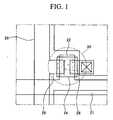
FIG. 1 is a partial enlarged view of a piece of electronic equipment including a general thin film transistor; -
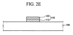
FIGs. 2A to 2E show a fabrication process of a substrate according to one embodiment; -
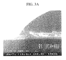
FIG. 3A is a photograph of pattern profiles of the photoresist when over-etching with respect to time by 30% according to Example 1 of the present embodiments; -
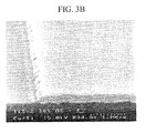
FIG. 3B is a photograph of a Cu/Ti layer when over-etching with respect to time by 30% according to Example 1 of the present embodiments; -
FIG. 3C is a cross-sectional views of a Cu/Ti layer when over-etching with respect to time by 30% according to Example 1 of the present embodiments; -
FIG. 4A is a photograph of pattern profiles of the photoresist when over-etching with respect to time by 60% according to Example 1 of the present embodiments; -
FIG. 4B is a photograph of a Cu/Ti layer when over-etching with respect to time by 60% according to Example 1 of the present embodiments; -
FIG. 4C is a cross-sectional views of a Cu/Ti layer when over-etching with respect to time by 60% according to Example 1 of the present embodiments; -
FIG. 5A is a photograph of pattern profiles of the photoresist when etching for 60 seconds according to Example 2 of the present embodiments; -
FIG. 5B is a photograph of pattern profiles of the photoresist when etching for 70 seconds according to Example 2 of the present embodiments; -
FIG. 6A is a photograph of pattern profiles of the photoresist when over-etching with respect to time by 43% according to Example 3 of the present embodiments; -
FIG. 6B is a photograph of a Cu/Ti layer when over-etching with respect to time by 43% according to Example 3 of the present embodiments; -
FIG. 6C is a cross-sectional views of a Cu/Ti layer when over-etching with respect to time by 43% according to Example 3 of the present embodiments; -
FIG. 7A is a photograph of pattern profiles of the photoresist when over-etching with respect to time by 60% according to Example 4 of the present embodiments; -
FIG. 7B is a photograph of a Cu/Ti layer when over-etching with respect to time by 60% according to Example 4 of the present embodiments; -
FIG. 7C is a cross-sectional views of a Cu/Ti layer when over-etching with respect to time by 60% according to Example 4 of the present embodiments; -
FIG. 8A is a photograph of pattern profiles of the photoresist when over-etching with respect to time by 40% according to Example 5 of the present embodiments; -
FIG. 8B is a photograph of a Cu/Ti layer when over-etching with respect to time by 40% according to Example 5 of the present embodiments; -
FIG. 8C is a cross-sectional views of a Cu/Ti layer when over-etching with respect to time by 60% according to Example 1 of the present embodiments; -
FIG. 9 is a graph of critical dimension loss when over-etching in Example 3 of the present embodiments; -
FIG. 10 is a graph of critical dimension loss when over-etching in Example 4 of the present embodiments; -
FIG. 11 is a graph showing etching time depending on the number of etched substrates according to Example 1 of the present embodiments; -
FIG. 12 is a graph showing etching time depending on the number of etched substrates according to Example 2 of the present embodiments; -
FIG. 1 is a partial enlarged view of a piece of electronic equipment, for example an organic light emitting diode (OLED) display including a general thin film transistor. - As shown in
FIG. 1 , thethin film transistor 20 includes agate electrode 22 connected to agate wire 21, asemiconductor layer 24 disposed on thegate electrode 22, asource electrode 26 connected to adata wire 25 on thesemiconductor layer 24, and adrain electrode 28 spaced by a predetermined interval from thesource electrode 26 on thesemiconductor layer 24. - The
gate electrode 22,source electrode 26, and drainelectrode 28 can be made of a metallic material. In order to minimize signal delay caused by the metallic material of thegate electrode 22,source electrode 26, and drainelectrode 28 of thethin film transistor 20, a multi-layered film including a copper layer, and a titanium or titanium alloy layer with low resistance should be applied. - A conventional etchant may cause critical dimension loss (CD-loss) of the copper/titanium or copper/titanium alloy layers depending on the number of etched substrates. In addition, the critical dimension loss (CD-loss) rate may not increase at a particular rate.
- Therefore, the conventional etchant has a problem of not uniformly controlling a pattern profile of a multi-layered film including a copper layer, and a titanium or titanium alloy layer, and it also decreases the yield rate and increases fabrication cost since it needs to be frequently replaced.
- According to one embodiment, an etchant is provided to etch the multi-layered film.
- The etchant includes a fluorine ion (F-) source; hydrogen peroxide (H2O2); a sulfate; a phosphate; an azole-based compound; and a solvent. The fluorine ion source is present at a concentration of from about 0.01 wt% to about 10 wt%, the hydrogen peroxide is present at a concentration of from about 1 wt% to about 20 wt%, the sulfate is present at a concentration of from about 0.1 wt% to about 10 wt%, the phosphate is present at a concentration of from about 0.1 wt% to about 10 wt%, the azole-based compound is present at a concentration of from about 0.01 wt% to about 5 wt%, and solvent is present in a balance amount.
- The fluorine ions play a role of etching the titanium or titanium alloy layer as shown in Reaction Scheme 1:
[Reaction Scheme 1] Ti + 4HF = TiF4 + H2↑
- In
Reaction Scheme 1, the titanium is easily reacted with the fluorine ions to produce titanium fluoride (TiF4). - In this embodiment, the fluorine ion source is provided by a fluoride selected from at least one from the group consisting of ammonium fluoride (NH4F), ammonium hydrogen fluoride (NH4HF2), potassium fluoride (KF), sodium fluoride (NaF), and combinations thereof as well as the above hydrogen fluoride (HF). The fluoride is dissociated in an aqueous solution to produce fluorine ions. When the fluorine ion source is present at a concentration of less than 0.01wt % the etch-rate of the titanium or titanium alloy is too slow. When the fluoride ion source is present at a concentration of more than 10 wt% then the etch rate of the titanium or titanium alloy is too fast. More preferably, the fluorine ion source is present at a concentration of from about 0.1 wt% to about 5 wt%.
- The hydrogen peroxide plays a role of etching of the copper layer as shown in
Reaction Schemes 2 and 3:
[Reaction Scheme 2] Cu + H2O2 = CuO + H2O
[Reaction Scheme 3] 2Cu + H2O2 = 2CuO + H2 ↑
- As shown in
Reaction Schemes 2 and 3, the oxygen of the hydrogen peroxide is reacted with copper to produce copper oxide (CuO), and water (H2O) or hydrogen gas (H2). The copper plays a role in producing the copper oxide. The hydrogen peroxide is present at a concentration of from about 1 wt% to about 20 wt%. When the hydrogen peroxide is present at a concentration of less than 1 wt% the etch rate of copper is too slow. When the hydrogen peroxide is present at a concentration of more than 20 wt% to the etch-rate of the copper is too fast. More preferably, the hydrogen peroxide is present at a concentration of from about 3 wt% to about 10 wt%. - The sulfate controls the etch-rate of the copper. The sulfate is used to suppress copper etching.
- The sulfate can be a compound of, for example, A2S04, AHS04, BS04 and combinations thereof where A is an alkali metal such as, for example, potassium (K), sodium (Na), and combinations thereof; ammonium (NH4 +); and combinations thereof, B is an alkaline-earth metal such as, for example, calcium (Ca), barium (Ba), and combinations thereof.. Preferably, the sulfate is selected from the group consisting of KHSO4, NaHSO4, CaSO4, BaSO4, (NH4)HSO4, and combinations thereof. The sulfate is present at a concentration of from about 0.1 wt% to about 10 wt%. When the sulfate is present at a concentration of less than 0.1 wt% the etch-rate of the copper may not be sufficiently suppressed. When the sulphate is present at a concentration of more than 10 wt% the etch-rate of the copper may be too slow. More preferably, the sulfate is present at a concentration of from about 0.5 wt% to about 5 wt%.
- The phosphate controls the etch-rate of the copper. As the concentration of the phosphate increases, the etch-rate of the copper increases.
- The phosphate is represented by DxHyPO4, wherein x and y are integers ranging from 0 to 3, wherein x+y=3, D is an alkali metal such as, for example, potassium (K), sodium (Na), and combinations thereof; an alkaline-earth metal such as, for example, calcium (Ca), barium (Ba), and combinations thereof; ammonium (NH4 +); and combinations thereof. Preferably, the phosphate is selected from the group consisting of K2HPO4, Na2HPO4, CaHPO4, BaHPO4, (NH4)H2PO4, (NH4)3PO4, and combinations thereof. The phosphate is present at a concentration of from about 0.1 wt% to about 10 wt%. When the phosphate is present at a concentration of less than 0.1 wt% the etch-rate of the copper may be too slow. When the phosphate is present at a concentration of more than 10 wt% the etch-rate of the copper may be too fast. More preferably, the phosphate is present at a concentration of from about 0.5 wt% to about 7 wt%.
- The azole-based compound acts as a reaction inhibitor of copper (a Cu inhibitor).
- The azole-based compound may be for example, an alkylimidazole such as methylimidazole (C4H6N2) (where the alkyl is a C1 to C7 alkyl); pyarazole; tolyltriazole; benzotriazole; aminotetrazole; and combinations thereof. The azole-based compound is present at a concentration of from about 0.01 wt% to about 5 wt%. When the azole-based compound is present at a concentration of less than 0.01 wt% the copper reaction and the etch-rate of the copper cannot be sufficiently suppressed. When the azole-based compound is present at a concentration of more than 5 wt% the copper reaction and the etch-rate of the copper may be too slow. More preferably, the azole-based compound is present at a concentration of about 0.5 wt% to about 3 wt%.
- The solvent can be purified water or de-ionized water.
- Copper ions produced by the etchant do not perform a reaction. Deterioration of etching performance with an increasing number of etched substrates can therefore be minimized. Uniform pattern profiles of the multi-layered film can therefore be obtained at a high yield, thereby reducing cost.
- In a preferred embodiment the multi-layered film has a structure in which a copper layer and a titanium or titanium alloy layer are multiply layered, and can be, for example, a double layer film of copper/titanium, a double layer film of copper/titanium alloy, a triple layer film of titanium/copper/titanium, a triple layer film of titanium alloy/copper/titanium alloy, and a quintuple layer film of titanium/titanium alloy/copper/ titanium/titanium alloy. The titanium alloy layer is a Ti-M alloy layer (wherein M is a transition metal such as Ni, etc.).
- According to another embodiment, provided is a method of fabricating an electric device including a thin film transistor that includes forming a multi-layered film by depositing titanium (Ti) or a titanium alloy (Ti alloy), and depositing copper (Cu); forming a selective mask by a photoresist method on the multi-layered film; and subjecting the masked multi-layered film to an etchant including fluorine ions (F-), hydrogen peroxide (H2O2), a sulfate, a phosphate, an azole-based compound, and a solvent to form a pattern.
-
FIGs. 2A to 2E show a fabrication process of a substrate according to one embodiment. - As shown in
FIG. 2A , a titanium ortitanium alloy layer 110 and acopper layer 120 are sequentially deposited on asubstrate 100 in not less than 2 layers to form a multi-layered film. Thetitanium layer 110 improves a close-contacting property between thecopper layer 120 having good conductivity and thesubstrate 100. Even though a gate electrode including the copper layer and titanium layer is described for better comprehension and ease of description, a gate electrode including a copper layer and a titanium alloy layer can also be applied. - The multi-layered film is the same as above.
- The copper is formed at a thickness from about 1000Å (0.1µm) to about 10.000Å (1µm), preferably at a thickness from about 2000Å (0.2µm) to about 5000Å (0.5µm). When the copper layer has a thickness of less than 1000 Å (0.1µm) current is not smoothly transferred and when the copper layer has a thickness of more than 10,000 Å (1µm) etching is difficult.
- The titanium or titanium alloy layer is formed at a thickness from about 10Å (0.001µm) to about 2000Å (0.2µm), preferably from about 40Å (0.004µm) to about 700Å (0.07µm). When the titanium or titanium alloy layer has a thickness of more than 10 Å (0.001µm) uniform deposition thickness can be obtained. Upper layers on the titanium or titanium alloy layer are not required to be thicker than 2000 Å (0.2µm).
- Subsequently, a
photoresist 130 is applied on the entire upper surface of the multi-layered film disposed on the substrate 100 (FIG. 2B ), and is subjected to selective exposure and development to form aphotoresist pattern 132 for a gate electrode so as to protect the multi-layered film by masking it (FIG. 2C ). - The masked multi-layered film is etched by the etchant (
FIG. 2D ). Herein, the etchant is the same as the above including the fluorine ions, hydrogen peroxide, sulfate, phosphate, and azole-based compound. - The
photoresist pattern 132 that remains on the gate electrode is removed using a stripper to form a gate electrode 142 (FIG. 2E ). - In the above description, formation of a gate electrode is described as an example, but the present embodiments are not limited thereto. The etching method can be applied to a source electrode and a data wire and/or a drain electrode as well as a gate electrode. Furthermore, it can be applied to all processes of pattern formation of a layer including a copper layer and a titanium or titanium alloy layer.
- The method of fabricating an electric device including a thin film transistor can etch a multi-layered film in a batch by using the etchant having the above composition and therefore process steps of a thin film transistor can be reduced, resulting in improvement of productivity and reduction of cost and inferiority rate.
- The fabricated thin film transistor can be applied to a thin film transistor-liquid crystal display (LCD) or organic light emitting diode (OLED) display. The connection structure of the thin film transistor and the above display devices and a method of fabricating the device are well known in the art to which the present embodiments pertain, and therefore their detailed descriptions are not provided.
- The following examples illustrate the present embodiments in more detail. However, it is understood that the present embodiments are not limited by these examples.
- A 200Å (0.02µm) titanium layer was deposited on a glass substrate, and a 2000Å (0.2µm) copper layer was deposited thereon to form a double-layer. Then, a photoresist was coated on the glass substrate deposited with the double-layer in order. The resulting product was selectively exposed and developed to form a mask for etching on the layers. An etchant was prepared by dissolving 0.3wt% of NH4F, 6wt% of H2O2, 3wt% of NaHSO4, 5wt% of (NH4)H2PO4, and 0.5wt% of 5-aminotetrazole in de-ionized water. The 200Å (0.02µm) titanium and 2000Å (0.2µm) copper layers were etched together by using the etchant in a spray swing method. The etching was performed at 25°C.
- A 200Å (0.02µm) titanium layer was deposited on a glass substrate, and a 2000Å (0.2µm) copper layer was deposited thereon to form a double-layer. Then, a photoresist was coated on the glass substrate deposited with the double-layer in order. The resulting product was selectively exposed and developed to form a mask for etching on the double-layer. An etchant was prepared by dissolving 0.3wt% of NH4F, 6wt% of H2O2, 5wt% of KHSO4, 3wt% of (NH4)3PO4, and 0.5wt% of 5-aminotetrazole in de-ionized water. The double-layer was etched at one time by using the etchant in a spray swing method. The etching was performed at 25°C.
- A 500Å (0.05µm) titanium layer, a 4000Å (0.4µm) copper layer, and a 500Å (0.05µm) titanium layer were sequentially deposited on a glass substrate to form a triple-layer. Then, a photoresist was coated on the glass substrate deposited with the triple-layer in order. The resulting product was selectively exposed and developed to form a mask for etching on the triple-layer. An etchant was prepared by dissolving 0.8wt% of HF, 10wt% of H2O2, 1wt% of KHSO4, 2wt% of (NH4)H2PO4, and 0.1wt% of 5-aminotetrazole in de-ionized water. The triple-layer was etched at one time by using the etchant in a spray swing method. The etching was performed at 30°C.
- A 500Å (0.05µm) titanium layer, a 4000Å (0.4µm) copper layer, and a 700Å (0.07µm) titanium layer were sequentially deposited on a glass substrate to form a triple-layer. Then, a photoresist was coated on the glass substrate deposited with the triple-layer in order. The resulting product was selectively exposed and developed to form a mask for etching on the triple-layer. An etchant was prepared by dissolving 0.8wt% of HF, 10wt% of H2O2, 1wt% of KHSO4, 2wt% of (NH4)H2PO4, and 0.1wt% of 5-aminotetrazole in de-ionized water. The triple-layer was etched at one time by using the etchant in a spray swing method. The etching was performed at 30°C.
- A 500Å (0.05µm) titanium layer, a 40Å (0.004µm) Ti-Ni alloy layer, a 4000Å (0.4µm) copper layer, a 40Å (0.004µm) Ti-Ni alloy layer, and a 700Å (0.07µm) titanium layer were sequentially deposited on a glass substrate to form a quintuple-layer. Then, a photoresist was coated on the glass substrate deposited with the quintuple-layer in order. The resulting product was selectively exposed and developed to form a mask for etching on the quintuple-layer. An etchant was prepared by dissolving 1wt% of HF, 10wt% of H2O2, 1wt% of KHSO4, 2wt% of (NH4)H2PO4, 1wt% of NH4HF2 and 0.1wt% of 5-aminotetrazole in de-ionized water. The quintuple-layer was etched at one time by using the etchant in a spray swing method. The etching was performed at 30°C.
- A 500Å (0.05µm) titanium layer, a 4000Å (0.04µm) copper layer, and a 500Å (0.05µm) titanium layer were sequentially deposited on a glass substrate to form a triple-layer. Then, a photoresist was coated on the glass substrate deposited with the triple-layer in order. The resulting product was selectively exposed and developed to form a mask for etching the triple-layer.
- An etchant was prepared by dissolving HF, H2O2, KHSO4, (NH4)H2PO4, and 5-aminotetrazole in an amount according to the following Table 1 in de-ionized water. The triple-layer was etched at one time by using the etchant in a spray swing method. The etching was performed at 30°C.
- The triple-layer was etched with the method as in Example 6, except using an etchant that was prepared by dissolving 1wt% of HF, 6wt% of H2O2, 1wt% of (NH4)H2PO4, and 0.1wt% of 5-aminotetrazole in de-ionized water as disclosed in Table 1, in a spray swing method. The etching was performed at 30°C.
Table 1 Etchant Composition HF H2O2 KHSO4 (NH4)H2PO4 5-aminotetrazol Comparative Example 1 1 6 - 1 0.1 Example 6 1 6 1 1 0.1 Example 7 1 6 2 1 0.1 Example 8 1 6 5 1 0.1 - The etching results of the multi-layered film of etchants according to Examples 1 to 5 such as etching time, degree of tapering, loss of critical dimension, edge sharpness, and change depending on time are provided in the following Table 2.
- Referring to Table 2, "just-etching" indicates how long it took for a bare glass substrate to be exposed to an etchant for the first time, and "etching time" indicates how long it took to reach a desired pattern until the etching end.
- The degree of tapering was determined by measuring the angle and length of the slope of copper and titanium layers with a field emission scanning electron microscope (FE-SEM).
- The critical dimension loss (CD-loss) was determined by measuring how much line width was decreased when the over-etching was carried out to 60% beyond finishing.
- In addition, the edge sharpness was determined by measuring the length of a tail formed when both edges of titanium and copper layers were dragged on the bottom, and "change depending on time" indicates the number of substrate sheets that can maintain an etching time measured by an end point detection system (EPD system) within ± 10%, when several sheets of substrates are etched with the same etchant.
Table 2 Etching Degree of tapering Loss of critical dimension (CD-loss) Edge sharpness Change depending on time Just etching Etching time Angle Length 60% Over etching Ti tail Ti length Cu length Number of sheets of etched substrates [unit] [sec] [sec] [°] [µm] [µm] [A] [µm] [µm] [sheet] Example 1 42 60 45 0.25 0.5 ~ 100 ~ 0.1 ~ 0.1 > 1000 Example 2 35 60 45 0.25 0.5 ~ 100 ~ 0.1 ~ 0.1 > 600 Example 3 60 80 60~70 ~0.2 1.4 0 <0.2 <0.2 - Example 4 62 86 60~70 ~0.2 ~1.4 0 <0.2 <0.2 - Example 5 43 60 50 ~0.2 ~1.4 (at 40% 0 <0.2 <0.2 - over-etching) - Referring to Table 2, it took 42 seconds and 35 seconds respectively for the bottom of the substrates of Examples 1 and 2 to be exposed, and 60 seconds for the etching to end. Their etching rates were all appropriate.
- The tapering degree of the substrates of Examples 1 and 2 all had an angle of 45° with a length of 0.25µm.
- The edge sharpness of Examples 1 and 2 showed a tail height of less than 100Å (0.01µm), and the titanium and copper layers had a length of less than 0.1µm.
- The pattern profiles of the multi-layered film etched by using the etchant according to Examples 1 to 5 was determined by measuring with a field emission scanning electron microscope (FE-SEM). The results are provided in
FIGs. 3 to 8 . -
FIG. 3A is a photograph of pattern profiles of the photoresist when over-etching with respect to time by 30% according to Example 1 of the present embodiments,FIG. 3B is a photograph of a Cu/Ti layer when over-etching with respect to time by 30% according to Example 1 of the present embodiments, andFIG. 3C is a cross-sectional views of a Cu/Ti layer when over-etching with respect to time by 30% according to Example 1 of the present embodiments. -
FIG. 4A is a photograph of pattern profiles of the photoresist when over-etching with respect to time by 60% according to Example 1 of the present embodiments,FIG. 4B is a photograph of a Cu/Ti layer when over-etching with respect to time by 60% according to Example 1 of the present embodiments, andFIG. 4C is a cross-sectional views of a Cu/Ti layer when over-etching with respect to time by 60% according to Example 1 of the present embodiments. -
FIG. 5A is a photograph of pattern profiles of the photoresist when etching for 60 seconds according to Example 2 of the present embodiments, andFIG. 5B is a photograph of pattern profiles of the photoresist when etching for 70 seconds according to Example 2 of the present embodiments. -
FIG. 6A is a photograph of pattern profiles of the photoresist when over-etching with respect to time by 43% according to Example 3 of the present embodiments,FIG. 6B is a photograph of a Cu/Ti layer when over-etching with respect to time by 43% according to Example 3 of the present embodiments, andFIG. 6C is a cross-sectional views of a Cu/Ti layer when over-etching with respect to time by 43% according to Example 3 of the present embodiments. -
FIG. 7A is a photograph of pattern profiles of the photoresist when over-etching with respect to time by 60% according to Example 4 of the present embodiments,FIG. 7B is a photograph of a Cu/Ti layer when over-etching with respect to time by 60% according to Example 4 of the present embodiments, andFIG. 7C is a cross-sectional views of a Cu/Ti layer when over-etching with respect to time by 60% according to Example 4 of the present embodiments. -
FIG. 8A is a photograph of pattern profiles of the photoresist when over-etching with respect to time by 40% according to Example 5 of the present embodiments,FIG. 8B is a photograph of a Cu/Ti layer when over-etching with respect to time by 40% according to Example 5 of the present embodiments, andFIG. 8C is a cross-sectional views of Cu/Ti layer when over-etching with respect to time by 60% according to Example 1 of the present embodiments. - As shown in
FIG. 4 to 9 , when Examples 1 to 5 were 60% over-etched, they had pattern width decrease of less than 0.5µm; that is to say, a bigger process margin vs. etching time. - The critical dimension loss when over-etching was measured in order to evaluate the etching effect of etchants in Examples 3 and 4 to the multi-layered film. The results are provided in
FIGs. 9 and10 . -
FIG. 9 is a graph of critical dimension loss when over-etching in Example 3 of the present embodiments, andFIG. 10 is a graph of critical dimension loss when over-etching in Example 4 of the present embodiments. As show inFIGs. 9 and10 , the critical dimension loss when over-etching was small in Examples 3 and 4. - Batch-etching results such as etching time and CD-loss of the Ti/Cu/Ti triple-layers according to Examples 6-8 and Comparative Example 1 are provided in the following Table 3.
Table 3 Etching Loss of critical dimension (CD-loss) Time [µm] [sec] 30% 60% 100% Over-etching Over-etching Over-etching Comparative Example 1 80 0.338 0.501 0.908 Example 6 50 0.327 0.511 0.679 Example 7 40 0.161 0.401 0.833 Example 8 25 0.425 0.871 1.295 - As shown in Table 3, the etchants including a sulfate in Examples 6 to 8 have an equal etching effect of CD-Loss compared with that of the Comparative Example 1. However, when the Ti/Cu/Ti triple layer was etched by using the etchants including the sulfate in Examples 6 to 8, the etching time was shorter than that of Comparative Example 1. Also, as the content of the sulfate in the etchant increases, etching time decreases.
- The etching process in Example 1 was repeated while continuously supplying the same kind of substrate. The etching time depending on the number of etched substrates according to Example 1 was measured, and the results are provided in
FIG. 11 . -
FIG. 11 is a graph showing etching time depending on the number of etched substrates according to Example 1 of the present embodiments. - As shown in
FIG. 11 , the etchant of Example 1 was able to etch more than 1000 sheets of substrates by reusing the same etchant. Even when more than 1000 sheets of substrates deposited with a 2000Å (0.2µm) copper layer and a 200Å (0.02µm) titanium layer were etched, the etchant can still be used, securing a longer replacement period. - The etching time depending on the number of etched substrates according to Example 2 was measured, and the results are provided in
FIG. 12 . -
FIG. 12 is a graph showing etching time depending on the number of etched substrates according to Example 2 of the present embodiments. - As shown in
FIG. 12 , when an etchant according to Example 2 of the present embodiments was used to etch a 5000Å (0.5µm) copper layer, it maintained etching performance for more than 600 sheets. Based on this result, it can etch more than 1500 sheets when it is used to etch a 2000Å (0.2µm) copper layer, which is 2.5 times that of the 5000Å (0.5µm) copper layer. The present embodiments can solve unstable etching performance of copper and titanium layers as the number of etched substrates increases. - Therefore, an etchant and a method of fabricating an electric device with a thin film transistor according to the present embodiments can have an effect on prolonging use time of an etchant for etching a multi-layered film having a structure in which a copper layer and a titanium or titanium alloy layer are multiply layered, in a batch, thereby increasing yield rate by improving a pattern profile, and decreasing fabrication cost by maintaining uniform etching performance, when it is repeatedly used to etch sheets of substrates and thereby postponing its replacement period.
- In addition, the etchant and the method of fabricating an electric device with a thin film transistor according to the present embodiments can simplify the application of copper with low resistance to an electronic device and thereby the electronic device can have improved characteristics such as high-aperture ratio, high-definition, and the like, and can also have reduced register-capacitor signal delay. Accordingly, it can be manufactured to be large-sized and have high quality.
- While the present embodiments have been described in connection with what is presently considered to be practical exemplary embodiments, it is to be understood that the present embodiments are not limited to the disclosed embodiments, but, on the contrary, is intended to cover various modifications and equivalent arrangements included within the scope of the appended claims.
Claims (13)
- An etchant comprising:a fluorine ion (F-) source;hydrogen peroxide (H2O2);a sulfate;a phosphate;an azole-based compound; anda solvent.
- The etchant of claim 1, wherein the fluorine ion source is present at a concentration of from 0.01 wt% to 10 wt%, the hydrogen peroxide is present at a concentration of from 1 wt% to 20 wt%, the sulfate is present at a concentration of from 0.1 wt% to 10 wt%, the phosphate is present at a concentration of from 0.1 wt% to 10 wt%, the azole-based compound is present at a concentration of from 0.01 wt% to 5 wt%, and the solvent is present in a balance amount.
- The etchant of claim 1 or Claim 2, wherein the fluorine ion (F-) source is selected from the group consisting of hydrogen fluoride (HF), ammonium fluoride (NH4F), ammonium hydrogen fluoride (NH4HF2), potassium fluoride (KF), sodium fluoride (NaF), and combinations thereof.
- The etchant of claim 1, 2 or 3 wherein the sulfate is a compound selected from of the group consisting of A2SO4, AHSO4, BSO4 and combinations thereof, wherein A is selected from the group consisting of an alkali metal, an ammonium ion (NH4 -), and combinations thereof, and wherein B is an alkaline-earth metal.
- The etchant of any preceding claim, wherein the phosphate is a compound of the formula DxHyPO4 wherein x and y are integers from 0 to 3, wherein x+y=3, and wherein D is selected from the group consisting of an alkali metal, an alkaline-earth metal, an ammonium ion (NH4 -), and combinations thereof.
- The etchant of according to any preceding claim, wherein the azole-based compound is selected from the group consisting of alkylimidazole, wherein the alkyl is a C1 to C7 alkyl, pyrazole, tolyltriazole, benzotriazole, aminotetrazole, and combinations thereof.
- The etchant of any preceding claim, wherein the solvent is purified water or de-ionized water.
- A method of fabricating an electric device comprising a thin film transistor substrate, comprising:forming a multi-layered film by depositing titanium (Ti) or a titanium alloy (Ti alloy), and copper (Cu);forming a selective mask by a photoresist method on the multi-layered film; andsubjecting the masked multi-layered film to an etchant including a fluorine ion (F-) source, hydrogen peroxide (H2O2), a sulfate, a phosphate, an azole-based compound, and a solvent to form a pattern.
- The method of claim 8, wherein the patterned multi-layered film is used to form a gate electrode of a thin film transistor.
- The method of claim 8 or 9, wherein the patterned multi-layered film is used for a source or drain electrode of a thin film transistor.
- The method of any of claims 8 to 10, wherein the substrate including a thin film transistor is applied to a thin film transistor-liquid crystal display (LCD).
- The method of any of claims 8 to 10 wherein the substrate including a thin film transistor is applied to an organic light emitting diode (OLED) display.
- The method of any of claims 8 to 12, wherein the multi-layered film comprises a copper (Cu) layer, and a titanium (Ti) or titanium alloy layer.
Applications Claiming Priority (1)
| Application Number | Priority Date | Filing Date | Title |
|---|---|---|---|
| KR1020070048182A KR100839428B1 (en) | 2007-05-17 | 2007-05-17 | Etching liquid and method for manufacturing substrate having thin film transistor using same |
Publications (2)
| Publication Number | Publication Date |
|---|---|
| EP1992720A1 true EP1992720A1 (en) | 2008-11-19 |
| EP1992720B1 EP1992720B1 (en) | 2011-11-09 |
Family
ID=39708333
Family Applications (1)
| Application Number | Title | Priority Date | Filing Date |
|---|---|---|---|
| EP08251301A Active EP1992720B1 (en) | 2007-05-17 | 2008-04-03 | Etchant and method for fabricating electric device including thin film transistor using the same |
Country Status (6)
| Country | Link |
|---|---|
| US (1) | US7737033B2 (en) |
| EP (1) | EP1992720B1 (en) |
| JP (1) | JP4843637B2 (en) |
| KR (1) | KR100839428B1 (en) |
| CN (1) | CN101307444B (en) |
| TW (1) | TWI383068B (en) |
Families Citing this family (28)
| Publication number | Priority date | Publication date | Assignee | Title |
|---|---|---|---|---|
| KR101456930B1 (en) * | 2008-06-27 | 2014-10-31 | 동우 화인켐 주식회사 | Etchant composition |
| KR101495683B1 (en) * | 2008-09-26 | 2015-02-26 | 솔브레인 주식회사 | Cu or Cu/Mo or Cu/Mo alloy electrode etching liquid in Liquid Crystal Display system |
| KR101560000B1 (en) | 2009-02-06 | 2015-10-13 | 동우 화인켐 주식회사 | Manufacturing method of an array substrate for liquid crystal display |
| CN102471898B (en) * | 2009-07-22 | 2014-11-05 | 东友精细化工有限公司 | Etchant composition for forming a metal line |
| WO2011010877A2 (en) * | 2009-07-22 | 2011-01-27 | 동우 화인켐 주식회사 | Etchant composition for the formation of a metal line |
| KR101733804B1 (en) | 2009-08-20 | 2017-05-08 | 동우 화인켐 주식회사 | Etching solution composition for formation of metal line |
| KR101602499B1 (en) * | 2009-07-22 | 2016-03-11 | 동우 화인켐 주식회사 | Etching solution composition for formation of metal line |
| KR101621549B1 (en) | 2009-11-18 | 2016-05-16 | 동우 화인켐 주식회사 | Manufacturing method of an array substrate for liquid crystal display |
| KR101709925B1 (en) * | 2010-01-28 | 2017-02-27 | 미쯔비시 가스 케미칼 컴파니, 인코포레이티드 | Etching liquid for a copper/titanium multilayer thin film |
| KR101608873B1 (en) | 2010-03-18 | 2016-04-05 | 삼성디스플레이 주식회사 | Etchant for metal wire and method for manufacturing metal wire using the same |
| KR20110109118A (en) | 2010-03-30 | 2011-10-06 | 삼성전자주식회사 | Titanium etchant composition and method for manufacturing semiconductor device using same |
| KR101825493B1 (en) | 2010-04-20 | 2018-02-06 | 삼성디스플레이 주식회사 | Etchant for electrode and method of fabricating thin film transistor array panel using the same |
| KR20110121121A (en) * | 2010-04-30 | 2011-11-07 | 동우 화인켐 주식회사 | Etching composition for metal film containing copper and titanium |
| KR20110123025A (en) * | 2010-05-06 | 2011-11-14 | 삼성전자주식회사 | Metal wiring etchant and metal wiring formation method using the same |
| US9580818B2 (en) | 2010-06-18 | 2017-02-28 | Mitsubishi Gas Chemical Company, Inc. | Etching liquid for film of multilayer structure containing copper layer and molybdenum layer |
| KR101813719B1 (en) | 2011-07-19 | 2017-12-29 | 엘지디스플레이 주식회사 | Manufacturing method of thin film transisotr array substrate |
| CN102955301B (en) * | 2011-08-19 | 2015-12-16 | 乐金显示有限公司 | For array base palte and the manufacture method thereof of liquid crystal indicator |
| KR101850066B1 (en) * | 2011-11-01 | 2018-04-19 | 엘지디스플레이 주식회사 | Method of fabricating array substrate for in-plane switching mode liquid crystal display device |
| JP2013105916A (en) * | 2011-11-14 | 2013-05-30 | Panasonic Corp | Wiring board manufacturing method and semiconductor element manufacturing method |
| KR20130081492A (en) * | 2012-01-09 | 2013-07-17 | 삼성디스플레이 주식회사 | Method of forming a metal pattern and method of manufacturing a display substrate |
| KR102028578B1 (en) * | 2012-12-24 | 2019-10-04 | 동우 화인켐 주식회사 | Method of preparing array of thin film transistor |
| JP6180298B2 (en) * | 2013-11-27 | 2017-08-16 | 株式会社Adeka | Etching solution composition and etching method |
| WO2017033915A1 (en) | 2015-08-26 | 2017-03-02 | 株式会社Adeka | Etching liquid composition and etching method |
| US10920143B2 (en) | 2015-08-26 | 2021-02-16 | Adeka Corporation | Etching liquid composition and etching method |
| CN106328544A (en) * | 2016-08-24 | 2017-01-11 | 浙江德汇电子陶瓷有限公司 | Patterning method of nitride ceramic copper-clad plate and nitride ceramic copper-clad plate |
| KR20190027019A (en) * | 2017-09-04 | 2019-03-14 | 삼성디스플레이 주식회사 | Etchant and fabrication method of metal pattern and thin film transistor substrate using the same |
| KR102109339B1 (en) * | 2017-12-15 | 2020-05-12 | (주)비에스엠신소재 | Method for manufacturing highly conductive fiber with improved magnetic susceptibility using electroless-electrolytic plating method |
| CN114639600B (en) * | 2020-12-16 | 2024-09-24 | 京东方科技集团股份有限公司 | Thin film patterning method and method for preparing display panel |
Citations (4)
| Publication number | Priority date | Publication date | Assignee | Title |
|---|---|---|---|---|
| US20030107023A1 (en) * | 2001-12-06 | 2003-06-12 | Lg.Philips Lcd Co., Ltd. | Etchant for etching metal wiring layers and method for forming thin film transistor by using the same |
| US20030124851A1 (en) * | 2001-12-31 | 2003-07-03 | Lg.Philips Lcd Co., Ltd. | Etching solution for etching Cu and Cu/Ti metal layer of liquid crystal display device and method of fabricating the same |
| US20040262569A1 (en) * | 2003-06-24 | 2004-12-30 | Lg.Philips Lcd Co., Ltd. | Etchant for etching double-layered copper structure and method of forming array substrate having double-layered copper structures |
| KR20060099089A (en) * | 2005-03-10 | 2006-09-19 | 엘지.필립스 엘시디 주식회사 | Metal wiring etching solution, metal wiring etching method using the same and manufacturing method of liquid crystal display device using the etching solution |
Family Cites Families (5)
| Publication number | Priority date | Publication date | Assignee | Title |
|---|---|---|---|---|
| JP3974305B2 (en) * | 1999-06-18 | 2007-09-12 | エルジー フィリップス エルシーディー カンパニー リミテッド | Etching agent, method for manufacturing electronic device substrate using the same, and electronic device |
| KR100795364B1 (en) * | 2004-02-10 | 2008-01-17 | 삼성전자주식회사 | Cleaning liquid composition for semiconductor substrate, cleaning method using same and manufacturing method of conductive structure |
| KR20050110470A (en) * | 2004-05-19 | 2005-11-23 | 테크노세미켐 주식회사 | Composition for cleaning a semiconductor substrate, method for cleaning a semiconductor substrate and method for manufacturing a semiconductor device using the same |
| KR101199533B1 (en) * | 2005-06-22 | 2012-11-09 | 삼성디스플레이 주식회사 | Echant and method for fabricating interconnection line and method for fabricating thin film transistor substrate using the same |
| US20080224092A1 (en) * | 2007-03-15 | 2008-09-18 | Samsung Electronics Co., Ltd. | Etchant for metal |
-
2007
- 2007-05-17 KR KR1020070048182A patent/KR100839428B1/en active Active
-
2008
- 2008-02-22 TW TW097106207A patent/TWI383068B/en active
- 2008-03-19 CN CN2008100868254A patent/CN101307444B/en active Active
- 2008-03-24 US US12/079,008 patent/US7737033B2/en active Active
- 2008-04-03 EP EP08251301A patent/EP1992720B1/en active Active
- 2008-04-15 JP JP2008105853A patent/JP4843637B2/en active Active
Patent Citations (4)
| Publication number | Priority date | Publication date | Assignee | Title |
|---|---|---|---|---|
| US20030107023A1 (en) * | 2001-12-06 | 2003-06-12 | Lg.Philips Lcd Co., Ltd. | Etchant for etching metal wiring layers and method for forming thin film transistor by using the same |
| US20030124851A1 (en) * | 2001-12-31 | 2003-07-03 | Lg.Philips Lcd Co., Ltd. | Etching solution for etching Cu and Cu/Ti metal layer of liquid crystal display device and method of fabricating the same |
| US20040262569A1 (en) * | 2003-06-24 | 2004-12-30 | Lg.Philips Lcd Co., Ltd. | Etchant for etching double-layered copper structure and method of forming array substrate having double-layered copper structures |
| KR20060099089A (en) * | 2005-03-10 | 2006-09-19 | 엘지.필립스 엘시디 주식회사 | Metal wiring etching solution, metal wiring etching method using the same and manufacturing method of liquid crystal display device using the etching solution |
Also Published As
| Publication number | Publication date |
|---|---|
| KR100839428B1 (en) | 2008-06-19 |
| TWI383068B (en) | 2013-01-21 |
| CN101307444B (en) | 2012-11-21 |
| CN101307444A (en) | 2008-11-19 |
| EP1992720B1 (en) | 2011-11-09 |
| US20090286360A1 (en) | 2009-11-19 |
| JP4843637B2 (en) | 2011-12-21 |
| US7737033B2 (en) | 2010-06-15 |
| TW200902762A (en) | 2009-01-16 |
| JP2008288575A (en) | 2008-11-27 |
Similar Documents
| Publication | Publication Date | Title |
|---|---|---|
| EP1992720B1 (en) | Etchant and method for fabricating electric device including thin film transistor using the same | |
| KR101199533B1 (en) | Echant and method for fabricating interconnection line and method for fabricating thin film transistor substrate using the same | |
| US8236704B2 (en) | Etchant and array substrate having copper lines etched by the etchant | |
| KR100480797B1 (en) | Etching solution to improve etch rate for copper molybdenum multilayers and etching method using the same | |
| US6582982B2 (en) | Composition for wiring, a wiring using the composition, manufacturing method thereof, a display using the wiring and a manufacturing method thereof | |
| US6445004B1 (en) | Composition for a wiring, a wiring using the composition, manufacturing method thereof, a display using the wiring and a manufacturing method thereof | |
| US7566404B2 (en) | Method of fabricating a thin film transistor | |
| JP2004193620A (en) | Etching solution for removing molybdenum residue from copper molybdenum film and etching method thereof | |
| KR20060099089A (en) | Metal wiring etching solution, metal wiring etching method using the same and manufacturing method of liquid crystal display device using the etching solution | |
| KR100459271B1 (en) | Etching Solutions for Cu Monolayer or Cu Molybdenum Multilayers and Method of Preparing the Same | |
| KR101026983B1 (en) | Etching Composition of Thin Film Transistor Liquid Crystal Display | |
| KR20180015688A (en) | Etching composition, method of forming a metal pattern and method of manufacturing a display substrate | |
| KR20130051239A (en) | Etching composition, method of forming a metal pattern and method of manufacturing a display substrate | |
| JP2007150107A (en) | Etching composition for thin film transistor liquid crystal display device | |
| KR100495807B1 (en) | Wiring composition, metal wiring using this composition and its manufacturing method, display device using this wiring and its manufacturing method | |
| KR101236133B1 (en) | A combinated etchant composition for aluminum(or aluminum alloy) layer and multilayer containing the same, molybdenum(or molybdenum alloy) layer and multilayer containing the same, and indium tin oxides layer | |
| KR101300971B1 (en) | Fabrication method of thin film transistor, etching solution composition used the method | |
| KR102639571B1 (en) | A manufacturing method of an array substrate for liquid crystal display | |
| KR20240098637A (en) | Composition for Etching Aluminum-Containing Metal Layer | |
| KR20250128721A (en) | Composition for Etching Molybdenum-Containing Metal Layer |
Legal Events
| Date | Code | Title | Description |
|---|---|---|---|
| PUAI | Public reference made under article 153(3) epc to a published international application that has entered the european phase |
Free format text: ORIGINAL CODE: 0009012 |
|
| 17P | Request for examination filed |
Effective date: 20080410 |
|
| AK | Designated contracting states |
Kind code of ref document: A1 Designated state(s): AT BE BG CH CY CZ DE DK EE ES FI FR GB GR HR HU IE IS IT LI LT LU LV MC MT NL NO PL PT RO SE SI SK TR |
|
| AX | Request for extension of the european patent |
Extension state: AL BA MK RS |
|
| RAP1 | Party data changed (applicant data changed or rights of an application transferred) |
Owner name: SAMSUNG MOBILE DISPLAY CO., LTD. |
|
| AKX | Designation fees paid |
Designated state(s): DE FR GB HU IT |
|
| GRAP | Despatch of communication of intention to grant a patent |
Free format text: ORIGINAL CODE: EPIDOSNIGR1 |
|
| GRAS | Grant fee paid |
Free format text: ORIGINAL CODE: EPIDOSNIGR3 |
|
| GRAA | (expected) grant |
Free format text: ORIGINAL CODE: 0009210 |
|
| AK | Designated contracting states |
Kind code of ref document: B1 Designated state(s): DE FR GB HU IT |
|
| REG | Reference to a national code |
Ref country code: GB Ref legal event code: FG4D |
|
| REG | Reference to a national code |
Ref country code: DE Ref legal event code: R096 Ref document number: 602008011232 Country of ref document: DE Effective date: 20120105 |
|
| PG25 | Lapsed in a contracting state [announced via postgrant information from national office to epo] |
Ref country code: IT Free format text: LAPSE BECAUSE OF FAILURE TO SUBMIT A TRANSLATION OF THE DESCRIPTION OR TO PAY THE FEE WITHIN THE PRESCRIBED TIME-LIMIT Effective date: 20111109 |
|
| PLBE | No opposition filed within time limit |
Free format text: ORIGINAL CODE: 0009261 |
|
| STAA | Information on the status of an ep patent application or granted ep patent |
Free format text: STATUS: NO OPPOSITION FILED WITHIN TIME LIMIT |
|
| 26N | No opposition filed |
Effective date: 20120810 |
|
| REG | Reference to a national code |
Ref country code: DE Ref legal event code: R097 Ref document number: 602008011232 Country of ref document: DE Effective date: 20120810 |
|
| REG | Reference to a national code |
Ref country code: FR Ref legal event code: TP Owner name: SAMSUNG DISPLAY CO., LTD., KR Effective date: 20121226 |
|
| REG | Reference to a national code |
Ref country code: GB Ref legal event code: 732E Free format text: REGISTERED BETWEEN 20130103 AND 20130109 |
|
| REG | Reference to a national code |
Ref country code: DE Ref legal event code: R082 Ref document number: 602008011232 Country of ref document: DE Representative=s name: GULDE HENGELHAUPT ZIEBIG & SCHNEIDER, DE |
|
| REG | Reference to a national code |
Ref country code: DE Ref legal event code: R082 Ref document number: 602008011232 Country of ref document: DE Representative=s name: GULDE HENGELHAUPT ZIEBIG & SCHNEIDER, DE Effective date: 20130201 Ref country code: DE Ref legal event code: R081 Ref document number: 602008011232 Country of ref document: DE Owner name: SAMSUNG DISPLAY CO., LTD., KR Free format text: FORMER OWNER: SAMSUNG MOBILE DISPLAY CO. LTD., SUWON, KR Effective date: 20130201 Ref country code: DE Ref legal event code: R082 Ref document number: 602008011232 Country of ref document: DE Representative=s name: GULDE & PARTNER PATENT- UND RECHTSANWALTSKANZL, DE Effective date: 20130201 Ref country code: DE Ref legal event code: R081 Ref document number: 602008011232 Country of ref document: DE Owner name: SAMSUNG DISPLAY CO., LTD., YONGIN-CITY, KR Free format text: FORMER OWNER: SAMSUNG MOBILE DISPLAY CO. LTD., SUWON, GYEONGGI, KR Effective date: 20130201 |
|
| PG25 | Lapsed in a contracting state [announced via postgrant information from national office to epo] |
Ref country code: HU Free format text: LAPSE BECAUSE OF FAILURE TO SUBMIT A TRANSLATION OF THE DESCRIPTION OR TO PAY THE FEE WITHIN THE PRESCRIBED TIME-LIMIT Effective date: 20080403 |
|
| REG | Reference to a national code |
Ref country code: FR Ref legal event code: PLFP Year of fee payment: 9 |
|
| REG | Reference to a national code |
Ref country code: FR Ref legal event code: PLFP Year of fee payment: 10 |
|
| REG | Reference to a national code |
Ref country code: FR Ref legal event code: PLFP Year of fee payment: 11 |
|
| P01 | Opt-out of the competence of the unified patent court (upc) registered |
Effective date: 20230515 |
|
| PGFP | Annual fee paid to national office [announced via postgrant information from national office to epo] |
Ref country code: FR Payment date: 20250321 Year of fee payment: 18 |
|
| PGFP | Annual fee paid to national office [announced via postgrant information from national office to epo] |
Ref country code: GB Payment date: 20250320 Year of fee payment: 18 |
|
| PGFP | Annual fee paid to national office [announced via postgrant information from national office to epo] |
Ref country code: DE Payment date: 20250320 Year of fee payment: 18 |