EP1992589A2 - Packaging of MEMS microphone - Google Patents
Packaging of MEMS microphone Download PDFInfo
- Publication number
- EP1992589A2 EP1992589A2 EP07255081A EP07255081A EP1992589A2 EP 1992589 A2 EP1992589 A2 EP 1992589A2 EP 07255081 A EP07255081 A EP 07255081A EP 07255081 A EP07255081 A EP 07255081A EP 1992589 A2 EP1992589 A2 EP 1992589A2
- Authority
- EP
- European Patent Office
- Prior art keywords
- substrate
- mems microphone
- conductive
- electrically connected
- conductive layer
- Prior art date
- Legal status (The legal status is an assumption and is not a legal conclusion. Google has not performed a legal analysis and makes no representation as to the accuracy of the status listed.)
- Withdrawn
Links
Images

Classifications
-
- B—PERFORMING OPERATIONS; TRANSPORTING
- B81—MICROSTRUCTURAL TECHNOLOGY
- B81C—PROCESSES OR APPARATUS SPECIALLY ADAPTED FOR THE MANUFACTURE OR TREATMENT OF MICROSTRUCTURAL DEVICES OR SYSTEMS
- B81C1/00—Manufacture or treatment of devices or systems in or on a substrate
- B81C1/00015—Manufacture or treatment of devices or systems in or on a substrate for manufacturing microsystems
- B81C1/00222—Integrating an electronic processing unit with a micromechanical structure
- B81C1/0023—Packaging together an electronic processing unit die and a micromechanical structure die
-
- B—PERFORMING OPERATIONS; TRANSPORTING
- B81—MICROSTRUCTURAL TECHNOLOGY
- B81B—MICROSTRUCTURAL DEVICES OR SYSTEMS, e.g. MICROMECHANICAL DEVICES
- B81B7/00—Microstructural systems ; Auxiliary parts of microstructural devices or systems
- B81B7/0032—Packages or encapsulation
- B81B7/0061—Packages or encapsulation suitable for fluid transfer from the MEMS out of the package or vice versa, e.g. transfer of liquid, gas, sound
-
- H—ELECTRICITY
- H05—ELECTRIC TECHNIQUES NOT OTHERWISE PROVIDED FOR
- H05K—PRINTED CIRCUITS; CASINGS OR CONSTRUCTIONAL DETAILS OF ELECTRIC APPARATUS; MANUFACTURE OF ASSEMBLAGES OF ELECTRICAL COMPONENTS
- H05K1/00—Printed circuits
- H05K1/18—Printed circuits structurally associated with non-printed electric components
- H05K1/181—Printed circuits structurally associated with non-printed electric components associated with surface mounted components
-
- B—PERFORMING OPERATIONS; TRANSPORTING
- B81—MICROSTRUCTURAL TECHNOLOGY
- B81B—MICROSTRUCTURAL DEVICES OR SYSTEMS, e.g. MICROMECHANICAL DEVICES
- B81B2201/00—Specific applications of microelectromechanical systems
- B81B2201/02—Sensors
- B81B2201/0257—Microphones or microspeakers
-
- B—PERFORMING OPERATIONS; TRANSPORTING
- B81—MICROSTRUCTURAL TECHNOLOGY
- B81B—MICROSTRUCTURAL DEVICES OR SYSTEMS, e.g. MICROMECHANICAL DEVICES
- B81B2207/00—Microstructural systems or auxiliary parts thereof
- B81B2207/09—Packages
- B81B2207/091—Arrangements for connecting external electrical signals to mechanical structures inside the package
- B81B2207/093—Conductive package seal
-
- H—ELECTRICITY
- H05—ELECTRIC TECHNIQUES NOT OTHERWISE PROVIDED FOR
- H05K—PRINTED CIRCUITS; CASINGS OR CONSTRUCTIONAL DETAILS OF ELECTRIC APPARATUS; MANUFACTURE OF ASSEMBLAGES OF ELECTRICAL COMPONENTS
- H05K1/00—Printed circuits
- H05K1/02—Details
- H05K1/14—Structural association of two or more printed circuits
- H05K1/141—One or more single auxiliary printed circuits mounted on a main printed circuit, e.g. modules, adapters
-
- H—ELECTRICITY
- H05—ELECTRIC TECHNIQUES NOT OTHERWISE PROVIDED FOR
- H05K—PRINTED CIRCUITS; CASINGS OR CONSTRUCTIONAL DETAILS OF ELECTRIC APPARATUS; MANUFACTURE OF ASSEMBLAGES OF ELECTRICAL COMPONENTS
- H05K2201/00—Indexing scheme relating to printed circuits covered by H05K1/00
- H05K2201/10—Details of components or other objects attached to or integrated in a printed circuit board
- H05K2201/10007—Types of components
- H05K2201/10083—Electromechanical or electro-acoustic component, e.g. microphone
-
- H—ELECTRICITY
- H10—SEMICONDUCTOR DEVICES; ELECTRIC SOLID-STATE DEVICES NOT OTHERWISE PROVIDED FOR
- H10W—GENERIC PACKAGES, INTERCONNECTIONS, CONNECTORS OR OTHER CONSTRUCTIONAL DETAILS OF DEVICES COVERED BY CLASS H10
- H10W90/00—Package configurations
- H10W90/701—Package configurations characterised by the relative positions of pads or connectors relative to package parts
- H10W90/751—Package configurations characterised by the relative positions of pads or connectors relative to package parts of bond wires
- H10W90/754—Package configurations characterised by the relative positions of pads or connectors relative to package parts of bond wires between a chip and a stacked insulating package substrate, interposer or RDL
-
- Y—GENERAL TAGGING OF NEW TECHNOLOGICAL DEVELOPMENTS; GENERAL TAGGING OF CROSS-SECTIONAL TECHNOLOGIES SPANNING OVER SEVERAL SECTIONS OF THE IPC; TECHNICAL SUBJECTS COVERED BY FORMER USPC CROSS-REFERENCE ART COLLECTIONS [XRACs] AND DIGESTS
- Y02—TECHNOLOGIES OR APPLICATIONS FOR MITIGATION OR ADAPTATION AGAINST CLIMATE CHANGE
- Y02P—CLIMATE CHANGE MITIGATION TECHNOLOGIES IN THE PRODUCTION OR PROCESSING OF GOODS
- Y02P70/00—Climate change mitigation technologies in the production process for final industrial or consumer products
- Y02P70/50—Manufacturing or production processes characterised by the final manufactured product
Definitions
- the present invention relates to a microelectromechanical system (MEMS) microphone. More particularly, the present invention relates to a package and a packaging assembly of the MEMS microphone.
- MEMS microelectromechanical system
- Capacitor microphones which are fabricated by MEMS technology have advantages of light weight, small volume, and good signal quality, so MEMS microphones have gradually become mainstream products of the mini-microphone.
- a "Microelectromechanical system package with environmental and interference shield” has been disclosed in US patent No. US 6,781,231 , which includes a MEMS microphone, a substrate, and a cover.
- the substrate has a surface for carrying the MEMS microphone.
- the cover includes a conductive layer having a central portion and a peripheral portion around the central portion. The peripheral portion of the cover is connected to the substrate to form a housing. The central portion of the cover and the substrate are separated by a space for accommodating the MEMS microphone.
- the housing has an acoustic hole to allow acoustic signals to reach the MEMS microphone.
- the present invention is directed to a package for a MEMS microphone, suitable for being mounted on the printed circuit board and converting an acoustic signal to an electronic signal.
- the present invention is also directed to a packaging assembly of a MEMS microphone, for converting the acoustic signal to the electronic signal.
- the present invention provides a package of a MEMS microphone including a substrate, a MEMS microphone, a sealing element, and at least a conductive connecting element.
- the substrate has at least a conductive layer and at least a dielectric layer disposed on the substrate.
- the MEMS microphone is arranged on a bottom surface of the substrate, and is electrically connected to the conductive layer of the substrate.
- the sealing element is arranged on the bottom surface of the substrate and around the MEMS microphone.
- the conductive connecting element is arranged on the bottom surface of the substrate.
- the present invention further provides a package of a MEMS microphone including a substrate, a MEMS microphone, a conductive sealing element, at least a conductive connecting element, and at least an acoustic hole.
- the substrate has at least a conductive layer and at least a dielectric layer disposed on the substrate.
- the MEMS microphone is disposed on a bottom surface of the substrate, and is electrically connected to the conductive layer of the substrate.
- the conductive sealing element is arranged on the bottom surface of the substrate, electrically connected to the conductive layer on the bottom surface of the substrate, and around the MEMS microphone.
- the conductive connecting element is arranged on the bottom surface of the substrate.
- the acoustic hole is arranged on the substrate, the acoustic hole has a metal layer on an inner wall thereof, and the acoustic hole passes through the substrate and is connected to the conductive layer of the substrate.
- the conductive sealing element is electrically connected to a conductive layer of the printed circuit board, and constructs an acoustic housing with the printed circuit board and the substrate.
- the present invention further provides a packaging assembly of a MEMS microphone including a substrate, a MEMS microphone, a sealing element, at least a conductive connecting element, and a printed circuit board.
- the substrate has at least one first conductive layer and at least a dielectric layer disposed on the substrate.
- the MEMS microphone is arranged on a bottom surface of the substrate and electrically connected to the first conductive layer of the substrate.
- the sealing element is arranged on the bottom surface of the substrate and around the MEMS microphone.
- the conductive connecting element is arranged on the bottom surface of the substrate.
- the printed circuit board includes a second conductive layer.
- the present invention further provides a packaging assembly of a MEMS microphone including a substrate, a MEMS microphone, a conductive sealing element, at least a conductive connecting element, at least an acoustic hole, and a printed circuit board.
- the substrate has at least a first conductive layer and at least a dielectric layer disposed on the substrate.
- the MEMS microphone is disposed on a bottom surface of the substrate and electrically connected to the first conductive layer of the substrate.
- the conductive sealing element is arranged on the bottom surface of the substrate, and is electrically connected to the first conductive layer on the bottom surface of the substrate and around the MEMS microphone.
- the conductive connecting element is arranged on the bottom surface of the substrate.
- the acoustic hole is arranged on the substrate, the acoustic hole has a metal layer on an inner wall thereof, and the acoustic hole passes through the substrate and is connected to the first conductive layer of the substrate.
- the printed circuit board includes a second conductive layer.
- a substrate is used to carry the MEMS microphone, and the conductive sealing element is used to connect the substrate to the printed circuit board.
- the conductive sealing element, the substrate, and the printed circuit board form an acoustic housing and an electromagnetic interference shield to accommodate the MEMS microphone and the integrated circuit chip (IC chip) therein.
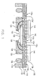
- FIG 1 is a cross-sectional view of a package of a MEMS microphone according to an embodiment of the present invention.
- FIG 2 is a partial cross-sectional view of the package of the MEMS microphone of FIG. 1 when being mounted on a printed circuit board.
- FIG 1 is a cross-sectional view of a package of a MEMS microphone according to an embodiment of the present invention
- FIG 2 is a partial cross-sectional view of the package of the MEMS microphone of FIG 1 when being mounted on a printed circuit board.
- the package of the MEMS microphone (hereafter referred to as the package) 100 of this embodiment is suitable for being mounted on a printed circuit board 200.
- the printed circuit board 200 includes a plurality of conductive layers 200a, a plurality of dielectric layers 200b stacked alternately with the conductive layers 200a, and a plurality of conductive vias 200c passing through the dielectric layers 200b and electrically connected to the conductive layers 200a.
- the package 100 includes a substrate 110, and the substrate 110 can be a multi-layer substrate fabricated by an FR-4 substrate lamination or ceramic substrate lamination process, and includes a plurality of conductive layers 110a, a plurality of dielectric layers 110b stacked alternately with the conductive layers 110a, and a plurality of conductive vias 110c passing through the dielectric layer 110b and electrically connected to the conductive layers 110a.
- the conductive layer 110a and the conductive vias 110c construct a conductive circuit of the substrate 110.
- the package 100 further includes a MEMS microphone 120 that is arranged on the bottom surface 112b opposite to the top surface 112a of the substrate 110, and has an acoustic pressure receiving surface 122.
- the MEMS microphone 120 can be adhered on the substrate 110, and is electrically connected to the substrate 110 by means of wire bonding.
- the MEMS microphone 120 is electrically connected to the substrate 110 through a plurality of wires 124, two dam bars 126 can be formed on the substrate 110 and the MEMS microphone 120 respectively by an encapsulation process, and an encapsulant 128 is formed in the scope or volume surrounded by the dam bars 126, so as to protect the MEMS microphone 120 and the wires 124.
- the package 100 further includes a conductive sealing element 130 that is arranged on the bottom surface 112b of the substrate 110, and around the MEMS microphone 120 for connecting the printed circuit board 200.
- the conductive sealing element 130 is, for example, a metal ring, a conductive adhesive ring, or a solder ring, in which the metal ring includes copper ring, and the solder ring can be formed by screen printing and solder reflowing processes.
- Two top and bottom sides of the conductive sealing element 130 respectively connect a pad 110a' constructed by the conductive layer 110a on the bottom surface 112b of the substrate 110 and a pad 200a' constructed by the conductive layer 200a of the surface 202 of the printed circuit board 200 ( Fig. 2 ).
- the shape of the conductive sealing element 130 can be circle, square, or polygon.
- the acoustic housing 132 has a plurality of acoustic holes 132a passing through the substrate 110 and the printed circuit board 200 respectively.
- the acoustic holes 130a can be formed in the substrate 110 and the printed circuit board 200 by drilling.
- the acoustic hole 132a has a metal layer 132a' on an inner wall thereof, passes through the substrate 110, and is connected to the conductive layer 110a on the top surface 112a and the conductive layer 110a on the bottom surface 112b of the substrate 110, so as to achieve a heat dissipation effect.
- the package 100 further includes an IC chip 142 arranged on the substrate 110 and electrically connected to the substrate 110.
- the MEMS microphone 120 can be disposed on the IC chip 142, i.e. indirectly disposed on the substrate 110 through being directly disposed on the IC chip 142.
- the MEMS microphone 120 can be adhered on the IC chip 142, and the IC chip 142 can be electrically connected to the substrate 110 by means of wire bonding.
- the IC chip 142 can be electrically connected to the MEMS microphone 120 by means of wire bonding.
- the package 100 can further include a plurality of IC chips 144 arranged on the substrate 110 and outside the acoustic housing 132.
- the IC chip 144 can be electrically connected to the substrate 110 by means of flip chip bonding.
- the package 100 can further include a plurality of conductive connecting elements 150, which are arranged on the substrate 110 for electrically connecting the pads of the substrate 110 to the pads of the printed circuit board 200.
- the conductive connecting elements 150 can be metal balls, for example, solder balls formed by solder-ball implantation process, and the conductive connecting elements 150 can also be metal leads, for example, copper leads.
- the conductive sealing element 130, the package 100, and the printed circuit board 200 construct or provide a packaging assembly 300 of MEMS microphone.
- the conductive layer 110a of the substrate 110, the conductive layer 200a of the printed circuit board 200, the conductive sealing element 130 and the connecting elements 150 can form a shield for preventing electromagnetic interference to the MEMS microphone 120 and the IC chip 142.
- the substrate is used to carry the MEMS microphone, and the substrate is connected to the printed circuit board through the conductive sealing element and the conductive connecting elements.
- the conductive sealing element, the substrate, and the printed circuit board form an acoustic housing and an electromagnetic interference shield to accommodate the MEMS microphone and the IC chip therein. Therefore, the present invention can package the MEMS microphone, and can be used in conjunction with the printed circuit board to provide the acoustic housing to the MEMS microphone, so as to facilitate the MEMS microphone to convert the acoustic signal to the electronic signal.
Landscapes
- Engineering & Computer Science (AREA)
- Microelectronics & Electronic Packaging (AREA)
- Manufacturing & Machinery (AREA)
- Computer Hardware Design (AREA)
- Electrostatic, Electromagnetic, Magneto- Strictive, And Variable-Resistance Transducers (AREA)
- Micromachines (AREA)
- Details Of Audible-Bandwidth Transducers (AREA)
Abstract
Description
- The present invention relates to a microelectromechanical system (MEMS) microphone. More particularly, the present invention relates to a package and a packaging assembly of the MEMS microphone.
- Along with the increasing demands for mobile phones, requirements relating to acoustic quality of mobile phones, and maturity of hearing aid technology, the demands for high-quality mini-microphone is rapidly growing. Capacitor microphones which are fabricated by MEMS technology have advantages of light weight, small volume, and good signal quality, so MEMS microphones have gradually become mainstream products of the mini-microphone.
- A "Microelectromechanical system package with environmental and interference shield" has been disclosed in US patent No.
US 6,781,231 , which includes a MEMS microphone, a substrate, and a cover. The substrate has a surface for carrying the MEMS microphone. The cover includes a conductive layer having a central portion and a peripheral portion around the central portion. The peripheral portion of the cover is connected to the substrate to form a housing. The central portion of the cover and the substrate are separated by a space for accommodating the MEMS microphone. The housing has an acoustic hole to allow acoustic signals to reach the MEMS microphone. - Accordingly, the present invention is directed to a package for a MEMS microphone, suitable for being mounted on the printed circuit board and converting an acoustic signal to an electronic signal.
- The present invention is also directed to a packaging assembly of a MEMS microphone, for converting the acoustic signal to the electronic signal.
- The present invention provides a package of a MEMS microphone including a substrate, a MEMS microphone, a sealing element, and at least a conductive connecting element. The substrate has at least a conductive layer and at least a dielectric layer disposed on the substrate. The MEMS microphone is arranged on a bottom surface of the substrate, and is electrically connected to the conductive layer of the substrate. The sealing element is arranged on the bottom surface of the substrate and around the MEMS microphone. The conductive connecting element is arranged on the bottom surface of the substrate. When the substrate is mounted on a printed circuit board by the sealing element and the conductive connecting element, the sealing element, the printed circuit board, and the substrate construct an acoustic housing, and the acoustic housing has at least an acoustic hole.
- The present invention further provides a package of a MEMS microphone including a substrate, a MEMS microphone, a conductive sealing element, at least a conductive connecting element, and at least an acoustic hole. The substrate has at least a conductive layer and at least a dielectric layer disposed on the substrate. The MEMS microphone is disposed on a bottom surface of the substrate, and is electrically connected to the conductive layer of the substrate. The conductive sealing element is arranged on the bottom surface of the substrate, electrically connected to the conductive layer on the bottom surface of the substrate, and around the MEMS microphone. The conductive connecting element is arranged on the bottom surface of the substrate. The acoustic hole is arranged on the substrate, the acoustic hole has a metal layer on an inner wall thereof, and the acoustic hole passes through the substrate and is connected to the conductive layer of the substrate. When the substrate is mounted on a printed circuit board by the conductive sealing element and the conductive connecting element, the conductive sealing element is electrically connected to a conductive layer of the printed circuit board, and constructs an acoustic housing with the printed circuit board and the substrate.
- The present invention further provides a packaging assembly of a MEMS microphone including a substrate, a MEMS microphone, a sealing element, at least a conductive connecting element, and a printed circuit board. The substrate has at least one first conductive layer and at least a dielectric layer disposed on the substrate. The MEMS microphone is arranged on a bottom surface of the substrate and electrically connected to the first conductive layer of the substrate. The sealing element is arranged on the bottom surface of the substrate and around the MEMS microphone. The conductive connecting element is arranged on the bottom surface of the substrate. The printed circuit board includes a second conductive layer. When the printed circuit board is connected with the substrate through the sealing element and the conductive connecting element, the sealing element, the printed circuit board, and the substrate construct or provide an acoustic housing, and the acoustic housing has at least an acoustic hole.
- The present invention further provides a packaging assembly of a MEMS microphone including a substrate, a MEMS microphone, a conductive sealing element, at least a conductive connecting element, at least an acoustic hole, and a printed circuit board. The substrate has at least a first conductive layer and at least a dielectric layer disposed on the substrate. The MEMS microphone is disposed on a bottom surface of the substrate and electrically connected to the first conductive layer of the substrate. The conductive sealing element is arranged on the bottom surface of the substrate, and is electrically connected to the first conductive layer on the bottom surface of the substrate and around the MEMS microphone. The conductive connecting element is arranged on the bottom surface of the substrate. The acoustic hole is arranged on the substrate, the acoustic hole has a metal layer on an inner wall thereof, and the acoustic hole passes through the substrate and is connected to the first conductive layer of the substrate. The printed circuit board includes a second conductive layer. When the substrate is mounted on the printed circuit board through the conductive sealing element and the conductive connecting element, the conductive sealing element is electrically connected to the second conductive layer of the printed circuit board, and constructs an acoustic housing with the printed circuit board and the substrate.
- In the present invention, a substrate is used to carry the MEMS microphone, and the conductive sealing element is used to connect the substrate to the printed circuit board. The conductive sealing element, the substrate, and the printed circuit board form an acoustic housing and an electromagnetic interference shield to accommodate the MEMS microphone and the integrated circuit chip (IC chip) therein.
- In order to make the aforementioned and other features and advantages of the present invention comprehensible, an embodiment accompanied with figures are described in detail below.
- It is to be understood that both the foregoing general description and the following detailed description are exemplary, and are intended to provide further explanation of the invention as claimed.
- The accompanying drawings are included to provide a further understanding of the invention, and are incorporated in and constitute a part of this specification. The drawings are schematic and illustrate an embodiment of the invention and, together with the description, serve to explain the principles of the invention.
-
FIG 1 is a cross-sectional view of a package of a MEMS microphone according to an embodiment of the present invention; and -
FIG 2 is a partial cross-sectional view of the package of the MEMS microphone ofFIG. 1 when being mounted on a printed circuit board. -
FIG 1 is a cross-sectional view of a package of a MEMS microphone according to an embodiment of the present invention, andFIG 2 is a partial cross-sectional view of the package of the MEMS microphone ofFIG 1 when being mounted on a printed circuit board. Referring toFIGs. 1 and2 , the package of the MEMS microphone (hereafter referred to as the package) 100 of this embodiment is suitable for being mounted on a printedcircuit board 200. The printedcircuit board 200 includes a plurality ofconductive layers 200a, a plurality ofdielectric layers 200b stacked alternately with theconductive layers 200a, and a plurality ofconductive vias 200c passing through thedielectric layers 200b and electrically connected to theconductive layers 200a. - The
package 100 includes asubstrate 110, and thesubstrate 110 can be a multi-layer substrate fabricated by an FR-4 substrate lamination or ceramic substrate lamination process, and includes a plurality of conductive layers 110a, a plurality ofdielectric layers 110b stacked alternately with the conductive layers 110a, and a plurality ofconductive vias 110c passing through thedielectric layer 110b and electrically connected to the conductive layers 110a. The conductive layer 110a and theconductive vias 110c construct a conductive circuit of thesubstrate 110. - The
package 100 further includes aMEMS microphone 120 that is arranged on thebottom surface 112b opposite to thetop surface 112a of thesubstrate 110, and has an acousticpressure receiving surface 122. In this embodiment, the MEMSmicrophone 120 can be adhered on thesubstrate 110, and is electrically connected to thesubstrate 110 by means of wire bonding. When the MEMSmicrophone 120 is electrically connected to thesubstrate 110 through a plurality ofwires 124, twodam bars 126 can be formed on thesubstrate 110 and theMEMS microphone 120 respectively by an encapsulation process, and anencapsulant 128 is formed in the scope or volume surrounded by thedam bars 126, so as to protect theMEMS microphone 120 and thewires 124. - The
package 100 further includes aconductive sealing element 130 that is arranged on thebottom surface 112b of thesubstrate 110, and around the MEMSmicrophone 120 for connecting the printedcircuit board 200. In this embodiment, theconductive sealing element 130 is, for example, a metal ring, a conductive adhesive ring, or a solder ring, in which the metal ring includes copper ring, and the solder ring can be formed by screen printing and solder reflowing processes. Two top and bottom sides of theconductive sealing element 130 respectively connect a pad 110a' constructed by the conductive layer 110a on thebottom surface 112b of thesubstrate 110 and apad 200a' constructed by theconductive layer 200a of thesurface 202 of the printed circuit board 200 (Fig. 2 ). The shape of theconductive sealing element 130 can be circle, square, or polygon. - When the
substrate 110 is mounted on the printedcircuit board 200 through theconductive sealing element 130, theconductive sealing element 130, the printedcircuit board 200, and thesubstrate 110 construct or provide anacoustic housing 132. Theacoustic housing 132 has a plurality ofacoustic holes 132a passing through thesubstrate 110 and the printedcircuit board 200 respectively. In addition, the acoustic holes 130a can be formed in thesubstrate 110 and the printedcircuit board 200 by drilling. In this embodiment, theacoustic hole 132a has ametal layer 132a' on an inner wall thereof, passes through thesubstrate 110, and is connected to the conductive layer 110a on thetop surface 112a and the conductive layer 110a on thebottom surface 112b of thesubstrate 110, so as to achieve a heat dissipation effect. - The
package 100 further includes anIC chip 142 arranged on thesubstrate 110 and electrically connected to thesubstrate 110. TheMEMS microphone 120 can be disposed on theIC chip 142, i.e. indirectly disposed on thesubstrate 110 through being directly disposed on theIC chip 142. In this embodiment, theMEMS microphone 120 can be adhered on theIC chip 142, and theIC chip 142 can be electrically connected to thesubstrate 110 by means of wire bonding. In another embodiment (not shown), theIC chip 142 can be electrically connected to theMEMS microphone 120 by means of wire bonding. - The
package 100 can further include a plurality ofIC chips 144 arranged on thesubstrate 110 and outside theacoustic housing 132. In this embodiment, theIC chip 144 can be electrically connected to thesubstrate 110 by means of flip chip bonding. - The
package 100 can further include a plurality of conductive connectingelements 150, which are arranged on thesubstrate 110 for electrically connecting the pads of thesubstrate 110 to the pads of the printedcircuit board 200. In this embodiment, the conductive connectingelements 150 can be metal balls, for example, solder balls formed by solder-ball implantation process, and the conductive connectingelements 150 can also be metal leads, for example, copper leads. - When the
substrate 110 is connected to the printedcircuit board 200 through theconductive sealing element 130 and the conductive connectingelements 150, theconductive sealing element 130, thepackage 100, and the printedcircuit board 200 construct or provide apackaging assembly 300 of MEMS microphone. In addition, the conductive layer 110a of thesubstrate 110, theconductive layer 200a of the printedcircuit board 200, theconductive sealing element 130 and the connectingelements 150 can form a shield for preventing electromagnetic interference to theMEMS microphone 120 and theIC chip 142. - To sum up, in the present invention, the substrate is used to carry the MEMS microphone, and the substrate is connected to the printed circuit board through the conductive sealing element and the conductive connecting elements. The conductive sealing element, the substrate, and the printed circuit board form an acoustic housing and an electromagnetic interference shield to accommodate the MEMS microphone and the IC chip therein. Therefore, the present invention can package the MEMS microphone, and can be used in conjunction with the printed circuit board to provide the acoustic housing to the MEMS microphone, so as to facilitate the MEMS microphone to convert the acoustic signal to the electronic signal.
- It will be apparent to those skilled in the art that various modifications and variations can be made to the structure of the present invention without departing from the scope of the invention. In view of the foregoing, it is intended that the present invention cover modifications and variations of this invention provided they fall within the scope of the following claims and their equivalents.
Claims (40)
- A package of a microelectromechanical system (MEMS) microphone, comprising:a substrate having at least a conductive layer and at least a dielectric layer disposed on the substrate;a MEMS microphone arranged on a bottom surface of the substrate and electrically connected to the conductive layer of the substrate;a sealing element arranged on the bottom surface of the substrate and around the MEMS microphone; andat least a conductive connecting element arranged on the bottom surface of the substrate,wherein when the substrate is mounted on a printed circuit board by the sealing element and the conductive connecting element, the sealing element, the printed circuit board, and the substrate construct an acoustic housing, and the acoustic housing has at least an acoustic hole.
- A package of the MEMS microphone as claimed in claim 1, characterized in that the substrate further comprises:at least a via arranged in the substrate.
- A package of the MEMS microphone as claimed in claim 2, characterized in that the via arranged in the substrate is a conductive via, and a plurality of the conductive layers is electrically connected by the conductive via passing through the dielectric layer.
- A package of the MEMS microphone as claimed in any preceding claim, characterized in that the sealing element is conductive, and is electrically connected to the conductive layer of the substrate.
- A package of the MEMS microphone as claimed in any preceding claim, characterized in that the acoustic hole passes through at least one of the substrate and the printed circuit board.
- A package of the MEMS microphone as claimed in any preceding claim, further characterized by comprising:at least an IC chip arranged on the bottom surface of the substrate, electrically connected to the substrate, and located in the acoustic housing, wherein the MEMS microphone is disposed on the IC chip, and is electrically connected to the IC chip or electrically connected to the conductive layer of the substrate.
- A package of the MEMS microphone as claimed in any of claims 1 to 5, further characterized by comprising:at least an IC chip arranged on the bottom surface of the substrate, electrically connected to the conductive layer of the substrate, and located in the acoustic housing,wherein the MEMS microphone is disposed on the bottom surface of the substrate, and is electrically connected to the IC chip or electrically connected to the conductive layer of the substrate.
- A package of the MEMS microphone as claimed in any of claims 1 to 5, further characterized by comprising:at least an IC chip arranged on the bottom surface of the substrate or a top surface of the substrate opposite to the bottom surface, electrically connected to the conductive layer of the substrate, and located outside the acoustic housing.
- A package of the MEMS microphone as claimed in any preceding claim, characterized in that the conductive connecting element is a solder ball or a solder lead.
- A package of the MEMS microphone as claimed in any of claims 4 to 9, characterized in that the sealing element is a metal ring or a solder ring.
- A package of the MEMS microphone as claimed in any of claims 4 to 10, characterized in that the sealing element is circle, square, or polygonal.
- A package of a MEMS microphone, comprising:a substrate having at least a conductive layer and at least a dielectric layer disposed on the substrate;a MEMS microphone disposed on a bottom surface of the substrate, and electrically connected to the conductive layer of the substrate;a conductive sealing element arranged on the bottom surface of the substrate, electrically connected to the conductive layer on the bottom surface of the substrate and around the MEMS microphone;at least a conductive connecting element arranged on the bottom surface of the substrate; andat least an acoustic hole arranged on the substrate, wherein the acoustic hole has a metal layer on an inner wall thereof, and the acoustic hole passes through the substrate and is connected to the conductive layer of the substrate,wherein when the substrate is mounted on a printed circuit board by the conductive sealing element and the conductive connecting element, the conductive sealing element is electrically connected to a conductive layer of the printed circuit board, and constructs an acoustic housing with the printed circuit board and the substrate.
- A package of the MEMS microphone as claimed in claim 12, characterized in that the substrate further comprises:at least a via arranged in the substrate.
- A package of the MEMS microphone as claimed in claim 13, characterized in that the via arranged in the substrate is a conductive via, and in that a plurality of the conductive layers is electrically connected by the conductive via passing through the dielectric layer.
- A package of the MEMS microphone as claimed in any of claims 12 to 14, further characterized by comprising:at least an IC chip disposed on the bottom surface of the substrate, electrically connected to the substrate, and located in the acoustic housing, wherein the MEMS microphone is disposed on the IC chip, and is electrically connected to the IC chip or electrically connected to the conductive layer of the substrate.
- A package of the MEMS microphone as claimed in any of claims 12 to 14, further characterized by comprising:at least an IC chip arranged on the bottom surface of the substrate, electrically connected to the substrate, and located in the acoustic housing, wherein the MEMS microphone is disposed on the bottom surface of the substrate, and is electrically connected to the IC chip or electrically connected to the conductive layer of the substrate.
- A package of the MEMS microphone as claimed in any of claims 12 to 14, further characterized by comprising:at least an IC chip arranged on the bottom surface of the substrate or a top surface of the substrate opposite to the bottom surface, electrically connected to the conductive layer of the substrate, and located outside the acoustic housing.
- A package of the MEMS microphone as claimed in any of claims 12 to 17, characterized in that the conductive connecting element is a solder ball or a solder lead.
- A package of the MEMS microphone as claimed in any of claims 12 to 17, characterized in that the conductive sealing element is a metal ring or a solder ring.
- A package of the MEMS microphone as claimed in any of claims 12 to 19, characterized in that the conductive sealing element is circle, square, or polygonal.
- A packaging assembly of a MEMS microphone, comprising:a substrate having at least a first conductive layer and at least a dielectric layer disposed on the substrate;a MEMS microphone arranged on a bottom surface of the substrate and electrically connected to the first conductive layer of the substrate;a sealing element arranged on the bottom surface of the substrate and around the MEMS microphone;at least a conductive connecting element arranged on the bottom surface of the substrate; anda printed circuit board comprising a second conductive layer,wherein when the printed circuit board is connected to the substrate through the sealing element and the conductive connecting element, the sealing element, the printed circuit board, and the substrate construct an acoustic housing, and the acoustic housing has at least an acoustic hole.
- A packaging assembly of the MEMS microphone as claimed in claim 21, characterized in that the substrate further comprises:at least a via arranged in the substrate.
- A packaging assembly of the MEMS microphone as claimed in claim 22, characterized in that the via arranged in the substrate is a conductive via, and a plurality of the first conductive layers is electrically connected by the conductive via passing through the dielectric layer.
- A packaging assembly of the MEMS microphone as claimed in any of claims 21 to 23, characterized in that the sealing element is conductive, and is electrically connected to the first conductive layer of the substrate and the second conductive layer of the printed circuit board.
- A packaging assembly of the MEMS microphone as claimed in any of claims 21 to 24, characterized in that the acoustic hole passes through at least one of the substrate and the printed circuit board.
- A packaging assembly of the MEMS microphone as claimed in any of claims 21 to 25, further characterized by comprising:at least an IC chip arranged on the bottom surface of the substrate, and electrically connected to the first conductive layer of the substrate, wherein the MEMS microphone is disposed on the IC chip, and electrically connected to the IC chip or the first conductive layer on the bottom surface of the substrate.
- A packaging assembly of the MEMS microphone as claimed in any of claims 21 to 25, further characterized by comprising:at least an IC chip arranged on the bottom surface of the substrate, electrically connected to the first conductive layer of the substrate, and located in the acoustic housing, wherein the MEMS microphone is disposed on the bottom surface of the substrate, and is electrically connected to the IC chip or electrically connected to the first conductive layer of the substrate.
- A packaging assembly of the MEMS microphone as claimed in any of claims 21 to 25, further characterized by comprising:at least an IC chip arranged on the bottom surface of the substrate or a top surface of the substrate opposite to the bottom surface, electrically connected to the first conductive layer of the substrate, and located outside the acoustic housing.
- A packaging assembly of the MEMS microphone as claimed in any of claims 21 to 28, characterized in that the conductive connecting element is a solder ball or a solder lead.
- A packaging assembly of the MEMS microphone as claimed in any of claims 21 to 29, characterized in that the sealing element is a metal ring or a solder ring.
- A packaging assembly of the MEMS microphone as claimed in any of claims 21 to 30, characterized in that the sealing element is circle, square, or polygonal.
- A packaging assembly of a MEMS microphone, comprising:a substrate having at least a first conductive layer and at least a dielectric layer disposed on the substrate;a MEMS microphone disposed on a bottom surface of the substrate and electrically connected to the first conductive layer of the substrate;a conductive sealing element arranged on the bottom surface of the substrate, electrically connected to the first conductive layer on the bottom surface of the substrate, and around the MEMS microphone;at least a conductive connecting element arranged on the bottom surface of the substrate;at least an acoustic hole arranged on the substrate, wherein the acoustic hole has a metal layer on an inner wall thereof, and the acoustic hole passes through the substrate and is connected to the first conductive layer of the substrate; anda printed circuit board comprising a second conductive layer,wherein when the substrate is mounted on the printed circuit board through the conductive sealing element and the conductive connecting element, the conductive sealing element is electrically connected to the second conductive layer of the printed circuit board, and constructs an acoustic housing with the printed circuit board and the substrate.
- A packaging assembly of the MEMS microphone as claimed in claim 32, characterized in that the substrate further comprises:at least a via arranged in the substrate.
- A packaging assembly of the MEMS microphone as claimed in claim 33, characterized in that the via arranged in the substrate is a conductive via, and a plurality of the first conductive layers is electrically connected by the conductive via passing through the dielectric layer.
- A packaging assembly of the MEMS microphone as claimed in claim 32, further characterized by comprising:at least an IC chip arranged on the bottom surface of the substrate, electrically connected to the substrate, and located in the acoustic housing, wherein the MEMS microphone is disposed on the IC chip, and is electrically connected to the IC chip or electrically connected to the first conductive layer on the bottom surface of the substrate.
- A packaging assembly of the MEMS microphone as claimed in any of claims 32 to 34, further characterized by comprising:at least an IC chip arranged on the bottom surface of the substrate, electrically connected to the substrate, and located in the acoustic housing, wherein the MEMS microphone is disposed on the bottom surface of the substrate, and is electrically connected to the IC chip or electrically connected to the first conductive layer of the substrate.
- A packaging assembly of the MEMS microphone as claimed in any of claims 32 to 34, further characterized by comprising:at least an IC chip arranged on the bottom surface of the substrate or a top surface of the substrate opposite to the bottom surface, electrically connected to the first conductive layer of the substrate, and located outside the acoustic housing.
- A packaging assembly of the MEMS microphone as claimed in any of claims 32 to 37, characterized in that the conductive connecting element is a solder ball or a solder lead.
- A packaging assembly of the MEMS microphone as claimed in any of claims 32 to 38, characterized in that the conductive sealing element is a metal ring or a solder ring.
- A packaging assembly of the MEMS microphone as claimed in any of claims 32 to 39, characterized in that the conductive sealing element is circle, square, or polygonal.
Applications Claiming Priority (1)
| Application Number | Priority Date | Filing Date | Title |
|---|---|---|---|
| TW096117299A TWI323242B (en) | 2007-05-15 | 2007-05-15 | Package and packageing assembly of microelectromechanical system microphone |
Publications (2)
| Publication Number | Publication Date |
|---|---|
| EP1992589A2 true EP1992589A2 (en) | 2008-11-19 |
| EP1992589A3 EP1992589A3 (en) | 2012-03-21 |
Family
ID=39719141
Family Applications (1)
| Application Number | Title | Priority Date | Filing Date |
|---|---|---|---|
| EP07255081A Withdrawn EP1992589A3 (en) | 2007-05-15 | 2007-12-28 | Packaging of MEMS microphone |
Country Status (3)
| Country | Link |
|---|---|
| US (1) | US7923791B2 (en) |
| EP (1) | EP1992589A3 (en) |
| TW (1) | TWI323242B (en) |
Cited By (3)
| Publication number | Priority date | Publication date | Assignee | Title |
|---|---|---|---|---|
| WO2010062820A3 (en) * | 2008-11-26 | 2010-09-10 | Analog Devices, Inc. | Side-ported mems microphone assembly |
| US9226052B2 (en) | 2013-01-22 | 2015-12-29 | Invensense, Inc. | Microphone system with non-orthogonally mounted microphone die |
| US20250250162A1 (en) * | 2024-02-01 | 2025-08-07 | AAC Kaitai Technologies (Wuhan) CO., LTD. | Mems speaker |
Families Citing this family (105)
| Publication number | Priority date | Publication date | Assignee | Title |
|---|---|---|---|---|
| TWI388038B (en) | 2009-07-23 | 2013-03-01 | 財團法人工業技術研究院 | Sensing element structure and manufacturing method |
| TWI434803B (en) | 2010-06-30 | 2014-04-21 | 財團法人工業技術研究院 | Integrated device of microelectromechanical component and circuit chip and manufacturing method thereof |
| EP2432249A1 (en) | 2010-07-02 | 2012-03-21 | Knowles Electronics Asia PTE. Ltd. | Microphone |
| US9215519B2 (en) * | 2010-07-30 | 2015-12-15 | Invensense, Inc. | Reduced footprint microphone system with spacer member having through-hole |
| US8611566B2 (en) * | 2011-03-01 | 2013-12-17 | Epcos Ag | MEMS-microphone |
| TWI484835B (en) * | 2011-04-12 | 2015-05-11 | Pixart Imaging Inc | Mems microphone device and method for making same |
| PH12014500377A1 (en) | 2011-08-18 | 2014-04-14 | Knowles Electronics Llc | Sensitivity adjustment apparatus and method for mems devices |
| US8853839B2 (en) | 2011-10-07 | 2014-10-07 | Analog Devices, Inc. | Air-release features in cavity packages |
| US9485560B2 (en) | 2012-02-01 | 2016-11-01 | Knowles Electronics, Llc | Embedded circuit in a MEMS device |
| US9402118B2 (en) | 2012-07-27 | 2016-07-26 | Knowles Electronics, Llc | Housing and method to control solder creep on housing |
| US9491539B2 (en) | 2012-08-01 | 2016-11-08 | Knowles Electronics, Llc | MEMS apparatus disposed on assembly lid |
| US9078063B2 (en) | 2012-08-10 | 2015-07-07 | Knowles Electronics, Llc | Microphone assembly with barrier to prevent contaminant infiltration |
| US9181086B1 (en) | 2012-10-01 | 2015-11-10 | The Research Foundation For The State University Of New York | Hinged MEMS diaphragm and method of manufacture therof |
| TWI549522B (en) * | 2012-12-14 | 2016-09-11 | 美律實業股份有限公司 | Mems microphone |
| US9467785B2 (en) | 2013-03-28 | 2016-10-11 | Knowles Electronics, Llc | MEMS apparatus with increased back volume |
| US9503814B2 (en) | 2013-04-10 | 2016-11-22 | Knowles Electronics, Llc | Differential outputs in multiple motor MEMS devices |
| US9301075B2 (en) | 2013-04-24 | 2016-03-29 | Knowles Electronics, Llc | MEMS microphone with out-gassing openings and method of manufacturing the same |
| US20180317019A1 (en) | 2013-05-23 | 2018-11-01 | Knowles Electronics, Llc | Acoustic activity detecting microphone |
| US10028054B2 (en) | 2013-10-21 | 2018-07-17 | Knowles Electronics, Llc | Apparatus and method for frequency detection |
| US10020008B2 (en) | 2013-05-23 | 2018-07-10 | Knowles Electronics, Llc | Microphone and corresponding digital interface |
| US9711166B2 (en) | 2013-05-23 | 2017-07-18 | Knowles Electronics, Llc | Decimation synchronization in a microphone |
| WO2014189931A1 (en) | 2013-05-23 | 2014-11-27 | Knowles Electronics, Llc | Vad detection microphone and method of operating the same |
| US9856136B2 (en) * | 2013-06-05 | 2018-01-02 | Intel Deutschland Gmbh | Chip arrangement and method for manufacturing a chip arrangement |
| US9386370B2 (en) | 2013-09-04 | 2016-07-05 | Knowles Electronics, Llc | Slew rate control apparatus for digital microphones |
| US9502028B2 (en) | 2013-10-18 | 2016-11-22 | Knowles Electronics, Llc | Acoustic activity detection apparatus and method |
| US9147397B2 (en) | 2013-10-29 | 2015-09-29 | Knowles Electronics, Llc | VAD detection apparatus and method of operating the same |
| US9527723B2 (en) * | 2014-03-13 | 2016-12-27 | STATS ChipPAC Pte. Ltd. | Semiconductor device and method of forming microelectromechanical systems (MEMS) package |
| DE102014204722A1 (en) * | 2014-03-14 | 2015-09-17 | Robert Bosch Gmbh | Electronic module and method and apparatus for manufacturing an electronic module |
| DE112015000731T5 (en) * | 2014-04-22 | 2017-02-02 | Robert Bosch Gmbh | Mems microphone assembly |
| US9831844B2 (en) | 2014-09-19 | 2017-11-28 | Knowles Electronics, Llc | Digital microphone with adjustable gain control |
| US9554214B2 (en) | 2014-10-02 | 2017-01-24 | Knowles Electronics, Llc | Signal processing platform in an acoustic capture device |
| US9743191B2 (en) | 2014-10-13 | 2017-08-22 | Knowles Electronics, Llc | Acoustic apparatus with diaphragm supported at a discrete number of locations |
| TWI539831B (en) | 2014-12-05 | 2016-06-21 | 財團法人工業技術研究院 | MEMS microphone package |
| US9743167B2 (en) | 2014-12-17 | 2017-08-22 | Knowles Electronics, Llc | Microphone with soft clipping circuit |
| US10045140B2 (en) | 2015-01-07 | 2018-08-07 | Knowles Electronics, Llc | Utilizing digital microphones for low power keyword detection and noise suppression |
| TW201640322A (en) | 2015-01-21 | 2016-11-16 | 諾爾斯電子公司 | Low power voice trigger for acoustic apparatus and method |
| US10121472B2 (en) | 2015-02-13 | 2018-11-06 | Knowles Electronics, Llc | Audio buffer catch-up apparatus and method with two microphones |
| US9866938B2 (en) | 2015-02-19 | 2018-01-09 | Knowles Electronics, Llc | Interface for microphone-to-microphone communications |
| US9800971B2 (en) | 2015-03-17 | 2017-10-24 | Knowles Electronics, Llc | Acoustic apparatus with side port |
| US9728510B2 (en) | 2015-04-10 | 2017-08-08 | Analog Devices, Inc. | Cavity package with composite substrate |
| US10291973B2 (en) | 2015-05-14 | 2019-05-14 | Knowles Electronics, Llc | Sensor device with ingress protection |
| WO2016183494A1 (en) | 2015-05-14 | 2016-11-17 | Knowles Electronics, Llc | Microphone with coined area |
| US9478234B1 (en) | 2015-07-13 | 2016-10-25 | Knowles Electronics, Llc | Microphone apparatus and method with catch-up buffer |
| US9794661B2 (en) | 2015-08-07 | 2017-10-17 | Knowles Electronics, Llc | Ingress protection for reducing particle infiltration into acoustic chamber of a MEMS microphone package |
| DE112016005317T5 (en) | 2015-11-19 | 2018-08-16 | Knowles Electronics, Llc | Differential MEMS microphone |
| US9516421B1 (en) | 2015-12-18 | 2016-12-06 | Knowles Electronics, Llc | Acoustic sensing apparatus and method of manufacturing the same |
| WO2017105851A1 (en) | 2015-12-18 | 2017-06-22 | Knowles Electronics, Llc | Microphone with hydrophobic ingress protection |
| WO2017136364A1 (en) | 2016-02-01 | 2017-08-10 | Knowles Electronics, Llc | Apparatus to bias mems motors |
| CN108702574B (en) | 2016-02-04 | 2021-05-25 | 美商楼氏电子有限公司 | Differential MEMS Microphone |
| US10349184B2 (en) | 2016-02-04 | 2019-07-09 | Knowles Electronics, Llc | Microphone and pressure sensor |
| US20170325012A1 (en) * | 2016-05-06 | 2017-11-09 | Infineon Technologies Ag | Device for detecting acoustic waves |
| WO2017205533A1 (en) | 2016-05-26 | 2017-11-30 | Knowles Electronics, Llc | Microphone device with integrated pressure sensor |
| WO2017222832A1 (en) | 2016-06-24 | 2017-12-28 | Knowles Electronics, Llc | Microphone with integrated gas sensor |
| US10499150B2 (en) | 2016-07-05 | 2019-12-03 | Knowles Electronics, Llc | Microphone assembly with digital feedback loop |
| US10206023B2 (en) | 2016-07-06 | 2019-02-12 | Knowles Electronics, Llc | Transducer package with through-vias |
| US10153740B2 (en) | 2016-07-11 | 2018-12-11 | Knowles Electronics, Llc | Split signal differential MEMS microphone |
| US9860623B1 (en) | 2016-07-13 | 2018-01-02 | Knowles Electronics, Llc | Stacked chip microphone |
| US10257616B2 (en) | 2016-07-22 | 2019-04-09 | Knowles Electronics, Llc | Digital microphone assembly with improved frequency response and noise characteristics |
| DE112017003785B4 (en) | 2016-07-27 | 2021-09-02 | Knowles Electronics, Llc | Microelectromechanical system (MEMS) device package |
| CN110024281B (en) | 2016-10-28 | 2024-05-07 | 三星电子株式会社 | Transducer assembly and method |
| WO2018106513A1 (en) | 2016-12-05 | 2018-06-14 | Knowles Electronics, Llc | Ramping of sensor power in a microelectromechanical system device |
| US10315912B2 (en) | 2016-12-28 | 2019-06-11 | Knowles Electronics, Llc | Microelectromechanical system microphone |
| US11218804B2 (en) | 2017-02-14 | 2022-01-04 | Knowles Electronics, Llc | System and method for calibrating microphone cut-off frequency |
| EP3379204B1 (en) | 2017-03-22 | 2021-02-17 | Knowles Electronics, LLC | Arrangement to calibrate a capacitive sensor interface |
| DE112018002672B4 (en) | 2017-05-25 | 2020-09-10 | Knowles Electronics, Llc | MICROPHONE HOUSING FOR FULLY COVERED ASIC AND WIRES AND PRODUCTION PROCESS THAT FOLLOWS THEM |
| WO2019005885A1 (en) | 2017-06-27 | 2019-01-03 | Knowles Electronics, Llc | Post linearization system and method using tracking signal |
| DE112018003794T5 (en) | 2017-07-26 | 2020-05-07 | Knowles Electronics, Llc | ACOUSTIC RELIEF IN MEMS |
| US10559293B2 (en) | 2017-09-08 | 2020-02-11 | Knowles Electronics, Llc | Digital microphone noise attenuation |
| CN111095949B (en) | 2017-09-18 | 2021-06-18 | 美商楼氏电子有限公司 | Method and microphone assembly for reducing noise in a sound transducer |
| DE112018005381T5 (en) | 2017-09-21 | 2020-06-25 | Knowles Electronics, Llc | INCREASED MEMS DEVICE IN A MICROPHONE WITH PENETRATION PROTECTION |
| CN107484093A (en) * | 2017-09-26 | 2017-12-15 | 深圳市芯易邦电子有限公司 | MEMS condenser microphone |
| WO2019099414A1 (en) | 2017-11-14 | 2019-05-23 | Knowles Electronics, Llc | Sensor package with ingress protection |
| CN112088539B (en) | 2018-03-21 | 2022-06-03 | 美商楼氏电子有限公司 | Microphone and control circuit therefor |
| CN112020865B (en) | 2018-04-26 | 2022-06-17 | 美商楼氏电子有限公司 | Acoustic components with acoustically transparent diaphragms |
| WO2019222106A1 (en) | 2018-05-18 | 2019-11-21 | Knowles Electronics, Llc | Systems and methods for reducing noise in microphones |
| WO2019246151A1 (en) | 2018-06-19 | 2019-12-26 | Knowles Electronics, Llc | Transconductance amplifier |
| WO2019246152A1 (en) | 2018-06-19 | 2019-12-26 | Knowles Electronics, Llc | Microphone assembly with reduced noise |
| WO2020072904A1 (en) | 2018-10-05 | 2020-04-09 | Knowles Electronics, Llc | Acoustic transducers with a low pressure zone and diaphragms having enhanced compliance |
| DE112019004979B4 (en) | 2018-10-05 | 2025-10-02 | Knowles Electronics, Llc | Method for manufacturing MEMS membranes comprising corrugations |
| US11206494B2 (en) | 2018-10-05 | 2021-12-21 | Knowles Electronics, Llc | Microphone device with ingress protection |
| WO2020076846A1 (en) | 2018-10-09 | 2020-04-16 | Knowles Electronics, Llc | Digital transducer interface scrambling |
| US11743647B2 (en) | 2018-12-11 | 2023-08-29 | Knowles Electronics, Llc. | Multi-rate integrated circuit connectable to a sensor |
| US11598821B2 (en) | 2019-01-22 | 2023-03-07 | Knowles Electronics, Llc. | Leakage current detection from bias voltage supply of microphone assembly |
| US11197104B2 (en) | 2019-01-25 | 2021-12-07 | Knowles Electronics, Llc | MEMS transducer including free plate diaphragm with spring members |
| US11122360B2 (en) | 2019-02-01 | 2021-09-14 | Knowles Electronics, Llc | Microphone assembly with back volume vent |
| EP3694222B1 (en) | 2019-02-06 | 2024-05-15 | Knowles Electronics, LLC | Sensor arrangement and method |
| US11778390B2 (en) | 2019-11-07 | 2023-10-03 | Knowles Electronics, Llc. | Microphone assembly having a direct current bias circuit |
| DE202020107185U1 (en) | 2019-12-23 | 2021-01-13 | Knowles Electronics, Llc | A microphone assembly incorporating a DC bias circuit with deep trench isolation |
| US11787690B1 (en) | 2020-04-03 | 2023-10-17 | Knowles Electronics, Llc. | MEMS assembly substrates including a bond layer |
| US11240600B1 (en) | 2020-11-12 | 2022-02-01 | Knowles Electronics, Llc | Sensor assembly and electrical circuit therefor |
| US11743666B2 (en) | 2020-12-30 | 2023-08-29 | Knowles Electronics, Llc. | Microphone assembly with transducer sensitivity drift compensation and electrical circuit therefor |
| US11671775B2 (en) | 2020-12-30 | 2023-06-06 | Knowles Electronics, Llc | Microphone assembly with transducer sensitivity drift compensation and electrical circuit therefor |
| US11916575B2 (en) | 2020-12-31 | 2024-02-27 | Knowleselectronics, Llc. | Digital microphone assembly with improved mismatch shaping |
| US11909387B2 (en) | 2021-03-17 | 2024-02-20 | Knowles Electronics, Llc. | Microphone with slew rate controlled buffer |
| US12240748B2 (en) | 2021-03-21 | 2025-03-04 | Knowles Electronics, Llc | MEMS die and MEMS-based sensor |
| US11897762B2 (en) | 2021-03-27 | 2024-02-13 | Knowles Electronics, Llc. | Digital microphone with over-voltage protection |
| US11528546B2 (en) | 2021-04-05 | 2022-12-13 | Knowles Electronics, Llc | Sealed vacuum MEMS die |
| US11540048B2 (en) | 2021-04-16 | 2022-12-27 | Knowles Electronics, Llc | Reduced noise MEMS device with force feedback |
| US11649161B2 (en) | 2021-07-26 | 2023-05-16 | Knowles Electronics, Llc | Diaphragm assembly with non-uniform pillar distribution |
| US11772961B2 (en) | 2021-08-26 | 2023-10-03 | Knowles Electronics, Llc | MEMS device with perimeter barometric relief pierce |
| US12552659B2 (en) | 2021-10-06 | 2026-02-17 | Knowles Electronics, Llc | MEMS die and MEMS-based sensor |
| US11780726B2 (en) | 2021-11-03 | 2023-10-10 | Knowles Electronics, Llc | Dual-diaphragm assembly having center constraint |
| TWI894636B (en) * | 2023-09-14 | 2025-08-21 | 万閎企業有限公司 | Chip package manufacturing method |
| TWI891063B (en) * | 2023-09-14 | 2025-07-21 | 万閎企業有限公司 | Chip package manufacturing method |
| US20250140626A1 (en) * | 2023-10-27 | 2025-05-01 | Texas Instruments Incorporated | Sensor electronic device |
Citations (2)
| Publication number | Priority date | Publication date | Assignee | Title |
|---|---|---|---|---|
| US20050189635A1 (en) | 2004-03-01 | 2005-09-01 | Tessera, Inc. | Packaged acoustic and electromagnetic transducer chips |
| US20070058826A1 (en) | 2005-09-13 | 2007-03-15 | Star Micronics Co., Ltd. | Condenser microphone |
Family Cites Families (24)
| Publication number | Priority date | Publication date | Assignee | Title |
|---|---|---|---|---|
| US5408534A (en) | 1992-03-05 | 1995-04-18 | Knowles Electronics, Inc. | Electret microphone assembly, and method of manufacturer |
| DK172085B1 (en) | 1995-06-23 | 1997-10-13 | Microtronic As | Micromechanical Microphone |
| US5889872A (en) | 1996-07-02 | 1999-03-30 | Motorola, Inc. | Capacitive microphone and method therefor |
| US5740261A (en) | 1996-11-21 | 1998-04-14 | Knowles Electronics, Inc. | Miniature silicon condenser microphone |
| FI105880B (en) | 1998-06-18 | 2000-10-13 | Nokia Mobile Phones Ltd | Fastening of a micromechanical microphone |
| US6088463A (en) | 1998-10-30 | 2000-07-11 | Microtronic A/S | Solid state silicon-based condenser microphone |
| CA2315417A1 (en) | 1999-08-11 | 2001-02-11 | Hiroshi Une | Electret capacitor microphone |
| US6522762B1 (en) | 1999-09-07 | 2003-02-18 | Microtronic A/S | Silicon-based sensor system |
| US6732588B1 (en) | 1999-09-07 | 2004-05-11 | Sonionmems A/S | Pressure transducer |
| JP3440037B2 (en) | 1999-09-16 | 2003-08-25 | 三洋電機株式会社 | Semiconductor device, semiconductor electret condenser microphone, and method of manufacturing semiconductor electret condenser microphone. |
| US7434305B2 (en) | 2000-11-28 | 2008-10-14 | Knowles Electronics, Llc. | Method of manufacturing a microphone |
| US6654473B2 (en) | 2001-05-09 | 2003-11-25 | Knowles Electronics, Llc | Condenser microphone |
| US6924429B2 (en) | 2001-08-17 | 2005-08-02 | Citizen Watch Co., Ltd. | Electronic device and production method therefor |
| US6781231B2 (en) | 2002-09-10 | 2004-08-24 | Knowles Electronics Llc | Microelectromechanical system package with environmental and interference shield |
| US6928178B2 (en) | 2002-12-17 | 2005-08-09 | Taiwan Carol Electronics Co., Ltd. | Condenser microphone and method for making the same |
| KR100543972B1 (en) * | 2003-02-08 | 2006-01-20 | 송기영 | Case bonding structure of condenser microphone and manufacturing method thereof |
| CN1922511B (en) | 2004-02-24 | 2010-09-22 | Faro科技有限公司 | Retroreflectors for window coverings |
| DE102004011148B3 (en) * | 2004-03-08 | 2005-11-10 | Infineon Technologies Ag | Microphone esp. semiconductor capacitor microphone for use in mobile telephones and the like having space between chip and substrate in pressure communication with space between chip and cover |
| EP1722596A4 (en) * | 2004-03-09 | 2009-11-11 | Panasonic Corp | ELECTRET CONDENSER MICROPHONE |
| US7373835B2 (en) * | 2005-01-31 | 2008-05-20 | Sanyo Electric Industries, Ltd. | Semiconductor sensor |
| US7202552B2 (en) * | 2005-07-15 | 2007-04-10 | Silicon Matrix Pte. Ltd. | MEMS package using flexible substrates, and method thereof |
| JP2007060389A (en) | 2005-08-25 | 2007-03-08 | Matsushita Electric Works Ltd | Silicon microphone package |
| KR100675023B1 (en) * | 2005-09-14 | 2007-01-30 | 주식회사 비에스이 | Condenser microphones and packaging method for the same |
| US7557417B2 (en) * | 2007-02-21 | 2009-07-07 | Infineon Technologies Ag | Module comprising a semiconductor chip comprising a movable element |
-
2007
- 2007-05-15 TW TW096117299A patent/TWI323242B/en not_active IP Right Cessation
- 2007-10-11 US US11/871,147 patent/US7923791B2/en not_active Expired - Fee Related
- 2007-12-28 EP EP07255081A patent/EP1992589A3/en not_active Withdrawn
Patent Citations (2)
| Publication number | Priority date | Publication date | Assignee | Title |
|---|---|---|---|---|
| US20050189635A1 (en) | 2004-03-01 | 2005-09-01 | Tessera, Inc. | Packaged acoustic and electromagnetic transducer chips |
| US20070058826A1 (en) | 2005-09-13 | 2007-03-15 | Star Micronics Co., Ltd. | Condenser microphone |
Cited By (5)
| Publication number | Priority date | Publication date | Assignee | Title |
|---|---|---|---|---|
| WO2010062820A3 (en) * | 2008-11-26 | 2010-09-10 | Analog Devices, Inc. | Side-ported mems microphone assembly |
| US8351634B2 (en) | 2008-11-26 | 2013-01-08 | Analog Devices, Inc. | Side-ported MEMS microphone assembly |
| US9226052B2 (en) | 2013-01-22 | 2015-12-29 | Invensense, Inc. | Microphone system with non-orthogonally mounted microphone die |
| US20250250162A1 (en) * | 2024-02-01 | 2025-08-07 | AAC Kaitai Technologies (Wuhan) CO., LTD. | Mems speaker |
| US12583739B2 (en) * | 2024-02-01 | 2026-03-24 | AAC Kaitai Technologies (Wuhan) CO., LTD. | MEMS speaker |
Also Published As
| Publication number | Publication date |
|---|---|
| TWI323242B (en) | 2010-04-11 |
| TW200844036A (en) | 2008-11-16 |
| US20080283942A1 (en) | 2008-11-20 |
| US7923791B2 (en) | 2011-04-12 |
| EP1992589A3 (en) | 2012-03-21 |
Similar Documents
| Publication | Publication Date | Title |
|---|---|---|
| US7923791B2 (en) | Package and packaging assembly of microelectromechanical system microphone | |
| CN101316461B (en) | Micro-electromechanical system microphone package and packaged components thereof | |
| US7868402B2 (en) | Package and packaging assembly of microelectromechanical system microphone | |
| US10381280B2 (en) | Semiconductor packages and methods for forming semiconductor package | |
| JP4185499B2 (en) | Semiconductor device | |
| CN101519183B (en) | Mems packaging including integrated circuit dies | |
| TWI395312B (en) | Package structure with MEMS components and its manufacturing method | |
| CN101316462B (en) | Micro-electromechanical system microphone package and packaged components thereof | |
| JP5216717B2 (en) | Small silicon condenser microphone and manufacturing method thereof | |
| EP1041633B1 (en) | Semiconductor device, method of manufacture thereof, circuit board, and electronic device | |
| US20120104629A1 (en) | Reversible top/bottom mems package | |
| US20160100256A1 (en) | Acoustic Assembly and Method of Manufacturing The Same | |
| CN105357616B (en) | Micro-electro-mechanical microphone packaging structure with three-dimensional substrate | |
| JP2008507123A (en) | Electronic device with integrated circuit | |
| KR20210131477A (en) | Semiconductor device | |
| US20170057808A1 (en) | Mems chip package and method for manufacturing the same | |
| CN109495831B (en) | Packaging structure of MEMS microphone and manufacturing method thereof | |
| TWI591779B (en) | Semiconductor package and semiconductor package manufacturing method thereof | |
| CN102020232A (en) | MEMS Acoustic Sensor Package Structure | |
| JP2007242813A (en) | Semiconductor device and manufacturing method thereof | |
| US20150296618A1 (en) | Substrate structure and manufacturing method thereof | |
| KR102472045B1 (en) | Semiconductor package | |
| KR20250154210A (en) | MEMS Microphone | |
| KR20260072433A (en) | MEMS Microphone | |
| JP2005159136A (en) | COB mounting frame, package mounting frame, and semiconductor device |
Legal Events
| Date | Code | Title | Description |
|---|---|---|---|
| PUAI | Public reference made under article 153(3) epc to a published international application that has entered the european phase |
Free format text: ORIGINAL CODE: 0009012 |
|
| AK | Designated contracting states |
Kind code of ref document: A2 Designated state(s): AT BE BG CH CY CZ DE DK EE ES FI FR GB GR HU IE IS IT LI LT LU LV MC MT NL PL PT RO SE SI SK TR |
|
| AX | Request for extension of the european patent |
Extension state: AL BA HR MK RS |
|
| PUAL | Search report despatched |
Free format text: ORIGINAL CODE: 0009013 |
|
| AK | Designated contracting states |
Kind code of ref document: A3 Designated state(s): AT BE BG CH CY CZ DE DK EE ES FI FR GB GR HU IE IS IT LI LT LU LV MC MT NL PL PT RO SE SI SK TR |
|
| AX | Request for extension of the european patent |
Extension state: AL BA HR MK RS |
|
| RIC1 | Information provided on ipc code assigned before grant |
Ipc: B81C 1/00 20060101ALI20120213BHEP Ipc: B81B 7/00 20060101AFI20120213BHEP |
|
| 17P | Request for examination filed |
Effective date: 20120828 |
|
| 17Q | First examination report despatched |
Effective date: 20121012 |
|
| AKX | Designation fees paid |
Designated state(s): AT BE BG CH CY CZ DE DK EE ES FI FR GB GR HU IE IS IT LI LT LU LV MC MT NL PL PT RO SE SI SK TR |
|
| STAA | Information on the status of an ep patent application or granted ep patent |
Free format text: STATUS: THE APPLICATION IS DEEMED TO BE WITHDRAWN |
|
| 18D | Application deemed to be withdrawn |
Effective date: 20160701 |