EP1992003B1 - Overcurrent switching apparatus - Google Patents
Overcurrent switching apparatus Download PDFInfo
- Publication number
- EP1992003B1 EP1992003B1 EP06706014.5A EP06706014A EP1992003B1 EP 1992003 B1 EP1992003 B1 EP 1992003B1 EP 06706014 A EP06706014 A EP 06706014A EP 1992003 B1 EP1992003 B1 EP 1992003B1
- Authority
- EP
- European Patent Office
- Prior art keywords
- current
- state
- contact system
- switching apparatus
- contact
- Prior art date
- Legal status (The legal status is an assumption and is not a legal conclusion. Google has not performed a legal analysis and makes no representation as to the accuracy of the status listed.)
- Expired - Lifetime
Links
Images
Classifications
-
- H—ELECTRICITY
- H01—ELECTRIC ELEMENTS
- H01H—ELECTRIC SWITCHES; RELAYS; SELECTORS; EMERGENCY PROTECTIVE DEVICES
- H01H71/00—Details of the protective switches or relays covered by groups H01H73/00 - H01H83/00
- H01H71/10—Operating or release mechanisms
- H01H71/12—Automatic release mechanisms with or without manual release
- H01H71/42—Induction-motor, induced-current, or electrodynamic release mechanisms
- H01H71/43—Electrodynamic release mechanisms
-
- H—ELECTRICITY
- H01—ELECTRIC ELEMENTS
- H01H—ELECTRIC SWITCHES; RELAYS; SELECTORS; EMERGENCY PROTECTIVE DEVICES
- H01H79/00—Protective switches in which excess current causes the closing of contacts, e.g. for short-circuiting the apparatus to be protected
-
- H—ELECTRICITY
- H01—ELECTRIC ELEMENTS
- H01H—ELECTRIC SWITCHES; RELAYS; SELECTORS; EMERGENCY PROTECTIVE DEVICES
- H01H3/00—Mechanisms for operating contacts
- H01H3/22—Power arrangements internal to the switch for operating the driving mechanism
- H01H3/222—Power arrangements internal to the switch for operating the driving mechanism using electrodynamic repulsion
Definitions
- the invention relates to an overcurrent switching device for medium or high voltage applications with current detection means for transferring a contact system assigned to them when a threshold current is exceeded from a first state to a second state, wherein the lying in a first branch current detection means are arranged downstream via coupling means actuating means, which Actuating means for transferring the lying in a second branch circuit contact system are formed from the first to the second state.
- An overcurrent switching device of the type mentioned is for example from the DE 100 02 870 A1 known. Other similar devices are out DE 10 47 915 B and from EP 1 526 560 A2 known. The closest prior art is the DE 3629040 A1 which describes a low-voltage vacuum switch of comparable operating principle.
- a connection conductor has a deformable portion as current detection means.
- the deformable section is deformed when a threshold current is exceeded such that a contact system is transferred from a first state to a second state.
- the deformable portion is also used here to form the contact system by forming the contact system together with a contact part.
- Object of the present invention is to provide an overcurrent switching device that can be flexibly and precisely designed according to the particular requirements.
- An essential advantage of the overcurrent switching device is that in her the current detection means and the coupling and actuating means are assemblies or elements by themselves, and thus can be produced by itself and measured accordingly; This also applies to the contact system, because it forms a system for itself, act on the actuating means. All this allows a precise adjustment and a large adjustment range of the threshold current, in which the contact system from its first to its second state can be transferred.
- the contact system can advantageously be used flexibly in that the first state of the contact system can be the open state and the second state can be the closed state of the contact system or vice versa, so that an opening or a closing overcurrent switching device depends on the respective requirements in a simple manner is trained.
- the advantageous possibility is given to effect a switching operation in the second current branch in the event of an overcurrent in the first current branch.
- an electromagnetic force acts in an advantageous manner between the parallel conductors with opposite current conduction, so that the deformable portion is deformed when a threshold current is exceeded by this force and transferred from a normal position to a working position.
- the threshold current is simple and flexible adjustable over the deformability of the deformable section.
- the coupling means comprise a blocking element fixedly connected to the deformable section.
- a blocking element for example a retaining pin, is a simple way of coupling the current-detecting means with the actuating means.
- the actuating means comprise a spring-loaded actuator having such a configuration that, in a blocking element in the normal position of the deformable portion, the actuator is held in a cocked spring position and released in a working position of the deformable portion.
- a spring-loaded actuator having such a configuration that, in a blocking element in the normal position of the deformable portion, the actuator is held in a cocked spring position and released in a working position of the deformable portion.
- the actuator may be designed in different ways, e.g. as a pestle.
- the actuating member is a movable, by means of the spring tensionable carriage with a rigidly connected guide rod.
- a slide is particularly durable or releasable by the blocking element.
- the contact system is formed of a rigidly connected to the actuating means moving contact for forming a conductive connection between a first and a second mating contact.
- the mating contacts can both be configured as a fixed contacts.
- Such a contact system can be converted in a simple manner by the actuating means from its first in its second state.
- the invention further relates to a bridging device for an electronic module, as described in the aforementioned earlier international patent application PCT / DE2005 / 001147 can be removed, and has set itself the task of such a bridging device for an electronic module so educate that it has a flexible structure with precisely adjustable threshold current.
- the object according to the invention serves a bridging device for an electronic module with an overcurrent switching device in one of the embodiments described above, wherein the current detection means for transfer of their associated contact system when a threshold current in the electronics module from a first state in which the electronics module to a Circuit arrangement is connected, in a second state in which the electronic module is bridged in the circuit arrangement, are formed.
- This bridging device advantageously allows a flexible construction with precisely adjustable threshold current.
- the bridging device thus forms an advantageous application of the overcurrent switching device according to the invention and can be used, for example, advantageously for bridging an electronic module according to the German Offenlegungsschrift DE 101 03 031 A1 deploy.
- the contact system is conductively connected to terminals of the electronic module.
- the current detection means detect the current of the electronic module.
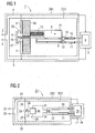
- FIG. 1 shows an overcurrent switching device ÜS1 a bridging device ÜB1 in an electronic module 1 with terminals 2 and 3, which via conductors 4 and 5 with a first mating contact 6 and a second mating contact 7, which are formed in the embodiment as the first fixed contact 6 and second fixed contact 7, and with a circuit unit 8 are connected.
- the circuit unit 8 comprises schematically illustrated electronic components 9, for example a plurality of switching elements such as IGBTs, diodes and an intermediate circuit capacitor of an inverter, which are connected to each other via current detection means in the form of connecting conductors 10, 11 and other connections not shown in the figures (compare the circuit unit of the above mentioned German Offenlegungsschrift DE 101 03 031 A1 ).
- the connecting conductors 10 and 11 are arranged in the circuit unit 8 such that an overcurrent occurring in the event of a fault flows through these connecting conductors 10 and 11.
- the connecting conductors 10 and 11 are designed as busbars and connected to one another at one end, so that a current flowing in the circuit unit 8 current through the busbars 10 and 11 is guided in opposite directions.
- the busbar 11 which is designed as a deformable busbar
- coupling means 12 and 13 in the form of a retaining pin 12 made of an insulating material as a blocking element 12 is fixed, which extends through a recess 13 in the busbar 10 therethrough.
- the coupling means 12, 13 are as actuating means 14, 15 and 18, a movable carriage 14, which is blocked by the retaining pin 12 and is biased by a spring 15 against an insulating body 16 of the electronic module, downstream.
- a recess 17 of the insulating body 16 extends through a guide rod 18 of the carriage 14, at the end of a moving contact 19 is arranged, which forms a contact system 20 together with the first fixed contact 6 and the second fixed contact 7.
- the Indian FIG. 1 shown state of the device corresponds to the normal Archzüstand the electronic module 1, in which usual operating currents flow within the electronic module 1.
- a fault for example by a Short circuit within the electronic module 1 or a wrong control of a switching element, can flow through the discharge of the capacitor of the circuit unit 8, a significantly higher current than the usual operating current in the electronic module.
- Due to the opposing leadership of the current through the busbars 10 and 11 is formed between these due to electromagnetic interaction, a force which pushes the busbars 10 and 11, while the deformable busbar 11 is deformed such that the fixed to the busbar 11 associated retaining pin 12 in the direction of the movement arrow A moves and releases the carriage 14.
- a short-circuit current in the electronic module 1 thus causes a closure of the contact system 20, so that between the terminals 2 and 3 of the electronic module 1 via the conductors 4 and 5 and the fixed contacts 6 and 7 and the moving contact 19, the remaining components of the electronic module 1 are bridged.
- a bridging of electronic modules in a circuit arrangement of a plurality of modules, for example in a series circuit, is particularly necessary if the functionality of the circuit arrangement is to be maintained in the event of failure of a single electronic module due to a malfunction.
- FIG. 2 shows a further embodiment of an overcurrent switching device ÜS2 a bridging device ÜB2 in an electronic module 21.
- Terminals'22 and 23 of the electronic module 21 are via conductors 24 and 25 with contacts 26 and 27 and connected to a circuit unit 28 with schematically represented electronic components 29, for example, figuratively not shown switching elements such as IGBTs, capacitors and diodes.
- Connecting conductors 30 and 31 and other connections not shown in the figures are provided for connecting the components 29.
- the connection conductors 30 and 31 are arranged in the circuit unit 28 such that an overcurrent occurring in the event of a fault flows through these connection conductors 30 and 31.
- the connecting conductors 30 and 31 are connected together at one end and together with a coil 32 current detection means 30, 31, 32.
- the coil 32 surrounds a portion of the connecting conductors 30, 31 and is via coupling means 33 and 34 in the form of connecting lines 33 and 34 coupled to actuating means 36 and 37.
- the actuating means 36, 37 comprise a control device 36 having a control connection 37 for controlling an electrical switch 38, which forms the contact system 39 with the contacts 26 and 27.
- FIG. 2 causes in case of failure of a semiconductor device driven by the capacitor of the circuit unit short-circuit current, an induction voltage in the coil 32, which is compared in the control device 36 with a threshold value. If the induction voltage is above the threshold value, then the switch 38 is closed via the control connection 37, so that the contact system 39 is closed off of the contacts 26, 27 and the switch 38, via the connection terminals 22, 23 and the conductors 24, 25 the remaining elements of the electronic module 21 are bridged. The switch 38 is thereby formed so that it after transferring to the second state, in the embodiment of the closed state, in remains in this state, even if after a decay of the short-circuit current, the induction voltage of the coil is no longer applied.
- a bridging of electronic modules in a circuit arrangement of several modules, for example a series circuit, is particularly necessary if the functionality of the series circuit is to be maintained in the event of failure of a single electronic module due to a malfunction.
- the switch 38 can be designed as a thyristor or as an electromagnet, wherein the control can be done either directly by the voltage induced in the coil 32 or depending on the desired precision, or via the control device 36, which can be configured for example as a simple trigger circuit.
Landscapes
- Emergency Protection Circuit Devices (AREA)
- Breakers (AREA)
Description
Die Erfindung betrifft eine Überstromschaltvorrichtung für Mittel- oder Hochspannungsanwendungen mit Strom-Detektionsmitteln zur Überführung eines ihnen zugeordneten Kontaktsystems bei Überschreiten eines Schwellenstromes aus einem ersten Zustand in einen zweiten Zustand, wobei den in einem ersten Stromzweig liegenden Strom-Detektionsmitteln über Kopplungsmittel Betätigungsmittel nachgeordnet sind, welche Betätigungsmittel zur Überführung des in einem zweiten Stromzweig liegenden Kontaktsystems aus dem ersten in den zweiten Zustand ausgebildet sind.The invention relates to an overcurrent switching device for medium or high voltage applications with current detection means for transferring a contact system assigned to them when a threshold current is exceeded from a first state to a second state, wherein the lying in a first branch current detection means are arranged downstream via coupling means actuating means, which Actuating means for transferring the lying in a second branch circuit contact system are formed from the first to the second state.
Eine Überstromschaltvorrichtung der eingangs genannten Art ist beispielsweise aus der
Aus der internationalen Patentanmeldung
Aufgabe der vorliegenden Erfindung ist es, eine Überstromschaltvorrichtung auszubilden, die flexibel und präzise den jeweils gestellten Anforderungen entsprechend ausgestaltet werden kann.Object of the present invention is to provide an overcurrent switching device that can be flexibly and precisely designed according to the particular requirements.
Erfindungsgemäß gelöst wird diese Aufgabe durch die Merkmale des Anspruchs 1.This object is achieved according to the invention by the features of claim 1.
Ein wesentlicher Vorteil der erfindungsgemäßen Überstromschaltvorrichtung besteht darin, dass bei ihr die Strom-Detektionsmittel sowie die Kopplungs- und Betätigungsmittel Baugruppen bzw. Elemente für sich darstellen, und somit für sich herstellbar und entsprechend bemessbar sind; dies gilt auch hinsichtlich des Kontaktsystems, weil dieses ein System für sich bildet, auf das die Betätigungsmittel einwirken. Dies alles ermöglicht eine präzise Einstellung und einen großen Einstellbereich des Schwellenstromes, bei dem das Kontaktsystem aus seinem ersten in seinen zweiten Zustand überführbar ist. Dabei ist das Kontaktsystem in vorteilhafter Weise insofern flexibel einsetzbar, dass der erste Zustand des Kontaktsystems der offene Zustand und der zweite Zustand der geschlossene Zustand des Kontaktsystems sein können oder umgekehrt, so dass in einfacher Weise abhängig von der jeweiligen Anforderungen eine öffnende oder eine schließende Überstromschaltvorrichtung ausgebildet ist. Dabei ist außerdem die vorteilhafte Möglichkeit gegeben, bei einem Überstrom in dem ersten Stromzweig einen Schaltvorgang in dem zweiten Stromzweig zu bewirken.An essential advantage of the overcurrent switching device according to the invention is that in her the current detection means and the coupling and actuating means are assemblies or elements by themselves, and thus can be produced by itself and measured accordingly; This also applies to the contact system, because it forms a system for itself, act on the actuating means. All this allows a precise adjustment and a large adjustment range of the threshold current, in which the contact system from its first to its second state can be transferred. In this case, the contact system can advantageously be used flexibly in that the first state of the contact system can be the open state and the second state can be the closed state of the contact system or vice versa, so that an opening or a closing overcurrent switching device depends on the respective requirements in a simple manner is trained. In addition, the advantageous possibility is given to effect a switching operation in the second current branch in the event of an overcurrent in the first current branch.
Bei einer derartigen Ausgestaltung wirkt in vorteilhafter Weise eine elektromagnetische Kraft zwischen den parallel verlaufenden Leitern mit gegensinniger Stromführung, so dass der deformierbare Abschnitt beim Überschreiten eines Schwellenstroms durch dieses Kraft deformiert und von einer Normalposition in eine Arbeitsposition überführt wird. Der Schwellenstrom ist dabei einfach und flexibel über die Deformierbarkeit des deformierbaren Abschnittes einstellbar.In such an embodiment, an electromagnetic force acts in an advantageous manner between the parallel conductors with opposite current conduction, so that the deformable portion is deformed when a threshold current is exceeded by this force and transferred from a normal position to a working position. The threshold current is simple and flexible adjustable over the deformability of the deformable section.
In weiterer Ausgestaltung der Erfindung umfassen die Kopplungsmittel ein mit dem deformierbaren Abschnitt fest verbundenes Blockierelement. Ein derartiges Blockierelement, beispielsweise ein Haltestift, ist eine einfache Möglichkeit zur Kopplung der Strom-Detektionsmittel mit den Betätigungsmitteln.In a further embodiment of the invention, the coupling means comprise a blocking element fixedly connected to the deformable section. Such a blocking element, for example a retaining pin, is a simple way of coupling the current-detecting means with the actuating means.
In einer bevorzugten Ausführungsform umfassen die Betätigungsmittel ein federbelastbares Betätigungsorgan mit einer derartigen Ausbildung, dass bei einem Blockierelement in der Normalposition des deformierbaren Abschnittes das Betätigungsorgan in einer Position mit gespannter Feder gehalten und in einer Arbeitsposition des deformierbaren Abschnittes freigegeben ist. Ein derartiges Betätigungsorgan ist in einfacher Weise durch das Blockierelement freigebbar, wodurch ein schnelles Überführen des Kontaktsystems aus seinem ersten in seinen zweiten Zustand vorteilhafterweise ermöglicht ist.In a preferred embodiment, the actuating means comprise a spring-loaded actuator having such a configuration that, in a blocking element in the normal position of the deformable portion, the actuator is held in a cocked spring position and released in a working position of the deformable portion. Such an actuator can be released in a simple manner by the blocking element, whereby a rapid transfer of the contact system from its first to its second state is advantageously possible.
Das Betätigungsorgan kann in unterschiedlicher Weise ausgebildet sein, z.B. als Stößel. In besonders bevorzugter Ausgestaltung ist das Betätigungsorgan ein beweglicher, mittels der Feder spannbarer Schlitten mit einer starr verbundenen Führungsstange. Ein solcher Schlitten ist besonders vorteilhaft durch das Blockierelement haltbar oder freigebbar.The actuator may be designed in different ways, e.g. as a pestle. In a particularly preferred embodiment, the actuating member is a movable, by means of the spring tensionable carriage with a rigidly connected guide rod. Such a slide is particularly durable or releasable by the blocking element.
In weiterer Ausgestaltung ist das Kontaktsystem aus einem mit den Betätigungsmitteln starr verbundenen Bewegkontakt zur Ausbildung einer leitenden Verbindung zwischen einem ersten und einem zweiten Gegenkontakt gebildet. Die Gegenkontakte können dabei beide als Festkontakte ausgebildet sein. Gegebenenfalls kann es auch vorteilhaft sein, einen Gegenkontakt als Festkontakt und den anderen Gegenkontakt als flexiblen Kontakt auszuführen, wobei der flexible Kontakt z.B. unter Verwendung einer flexiblen Anschlussleitung gewonnen sein kann. Ein derartiges Kontaktsystem ist in einfacher Weise durch die Betätigungsmittel aus seinem ersten in seinem zweiten Zustand überführbar.In a further embodiment, the contact system is formed of a rigidly connected to the actuating means moving contact for forming a conductive connection between a first and a second mating contact. The mating contacts can both be configured as a fixed contacts. Optionally, it may also be advantageous to have a mating contact to perform as a fixed contact and the other mating contact as a flexible contact, wherein the flexible contact can be obtained, for example, using a flexible connection cable. Such a contact system can be converted in a simple manner by the actuating means from its first in its second state.
Die Erfindung betrifft ferner eine Überbrückungsvorrichtung für ein Elektronikmodul, wie sie der eingangs erwähnten älteren internationalen Patentanmeldung
Zur Lösung der Aufgabe dient erfindungsgemäß eine Überbrückungsvorrichtung für ein Elektronikmodul mit einer Überstromschaltvorrichtung in einer der voranstehend beschriebenen Ausgestaltungen, wobei die Strom-Detektionsmitteln zur Überführung des ihnen zugeordneten Kontaktsystems bei Überschreiten eines Schwellenstromes in dem Elektronikmodul aus einem ersten Zustand, in welchem das Elektronikmodul an eine Schaltungsanordnung angeschlossen ist, in einen zweiten Zustand, in welchem das Elektronikmodul in der Schaltungsanordnung überbrückt ist, ausgebildet sind. Diese Überbrückungsvorrichtung ermöglicht in vorteilhafter Weise einen flexiblen Aufbau mit präzise einstellbarem Schwellenstrom. Die Überbrückungsvorrichtung bildet somit eine vorteilhafte Anwendung der erfindungsgemäßen Überstromschaltvorrichtung und lässt sich beispielsweise mit Vorteil zum Überbrücken eines Elektronikmoduls gemäß der deutschen Offenlegungsschrift
In weiterer Ausgestaltung ist das Kontaktsystem mit Anschlussklemmen des Elektronikmoduls leitend verbunden. Dadurch ist in einfacher Weise die Überbrückung des Elektronikmoduls beim Überschreiten des Schwellenstromes durch Ausbildung einer leitenden Verbindung zwischen den Anschlussklemmen über das Kontaktsystem gewährleistet.In a further embodiment, the contact system is conductively connected to terminals of the electronic module. As a result, the bridging of the electronic module when exceeding the threshold current is ensured by forming a conductive connection between the terminals via the contact system in a simple manner.
In weiterer Ausgestaltung der Erfindung erfassen die Strom-Detektionsmittel den Strom des Elektronikmoduls.In a further embodiment of the invention, the current detection means detect the current of the electronic module.
Die Erfindung wird im Folgenden anhand der Zeichnung und von Ausführungsbeispielen mit Bezug auf die beiliegenden Figuren näher erläutert. Es zeigen:
- Figur 1
- eine schematische Darstellung einer erfindungsgemäßen Überströmschaltvorrichtung in einer ersten Ausgestaltung einer Überbrückungsvorrichtung gemäß einer ersten Ausführungsform;
- Figur 2
- eine schematische Darstellung, einer Überstromschaltvorrichtung in einer zweiten Ausgestaltung einer Überbrückungsvorrichtung gemäß einer zweiten Ausführungsform.
- FIG. 1
- a schematic representation of an overflow switching device according to the invention in a first embodiment of a lock-up device according to a first embodiment;
- FIG. 2
- a schematic representation of an overcurrent switching device in a second embodiment of a lock-up device according to a second embodiment.
Der in der
In dem Ausführungsbeispiel der
- ÜB1, ÜB2ÜB1, ÜB2
- Überbrückungsvorrichtungenbridging devices
- ÜS1, ÜS2ÜS1, ÜS2
- ÜberstromschaltvorrichtungenOvercurrent switching devices
- 11
- Elektronikmodulelectronic module
- 2, 32, 3
- Anschlussklemmenterminals
- 4, 54, 5
- Leiterladder
- 66
- Erster FestkontaktFirst fixed contact
- 77
- Zweiter FestkontaktSecond fixed contact
- 88th
- Schaltungseinheitcircuit unit
- 99
- elektronische Bauteileelectronic components
- 10, 1110, 11
- Stromschienenbusbars
- 1212
- Haltestiftretaining pin
- 1313
- Durchführungexecution
- 1414
- Schlittencarriage
- 1515
- Federfeather
- 1616
- Isolierkörperinsulator
- 1717
- Durchführungexecution
- 1818
- Führungsstangeguide rod
- 1919
- Bewegkontaktmoving contact
- 2020
- KontaktsystemContact system
- 2121
- Elektronikmodulelectronic module
- 22, 2322, 23
- Anschlussklemmenterminals
- 24, 2524, 25
- Leiterladder
- 26, 2726, 27
- Kontaktecontacts
- 2828
- Schaltungseinheitcircuit unit
- 2929
- Bauteilecomponents
- 30, 3130, 31
- Verbindungsleiterconnecting conductors
- 3232
- SpuleKitchen sink
- 33, 3433, 34
- Anschlussleitungenconnecting cables
- 3535
- elektrische Schaltvorrichtungelectrical switching device
- 3636
- Steuerungsvorrichtungcontrol device
- 3737
- Steuerungsverbindungcontrol connection
- 3838
- Schaltkontaktswitching contact
- 3939
- KontaktsystemContact system
- A, BA, B
- Bewegungspfeilemovement arrows
Claims (8)
- Overcurrent switching apparatus for medium-voltage or high-voltage applications having current detection means (10, 11) for switching a contact system (20), which is associated with them, from a first state to a second state when a threshold current is exceeded, wherein the current detection means (10, 11) which are located in a first current branch are followed via coupling means (12, 13, 33, 34) by operating means (14, 15, 18) which are designed to switch the contact system (20, 39), which is located in a second current branch, from the first state to the second state wherein the current detection means (10, 11) comprise two busbar sections (10, 11) which run parallel to one another, in which the current is carried in opposite senses and of which at least one section (11) can be deformed, wherein the deformable section (11) can be changed from a normal position to an operating position by the threshold current being exceeded.
- Overcurrent switching apparatus according to Claim 1, characterized in that
the coupling means (12, 13) comprise a blocking element (12) which is firmly connected to the deformable section (11). - Overcurrent switching apparatus according to Claim 2, characterized in that
the operating means (14, 15, 18) comprise an operating member (14) which can be spring-loaded and is designed such that, when a blocking element (12) is in the normal position of the deformable section (11), the operating member (14) is held in a position with a stressed spring (15) and is released in an operating position of the deformable section (11). - Overcurrent switching apparatus according to Claim 3, characterized in that
the operating member (14) is a moving carriage (14) which can be stressed by means of the spring (15) and has a rigidly connected guide rod (18). - Overcurrent switching apparatus according to one of the preceding claims,
characterized in that
the contact system (20) is formed from a moving contact (19) which is rigidly connected to the operating means (14, 15, 18), in order to form a conductive connection between a first and a second opposing contact (6, 7). - Bridging apparatus for an electronics module (1) having an overcurrent switching apparatus according to one of the preceding claims, wherein the current detection means (10, 11) are designed to switch the contact system (20) associated with them from a first state, in which the electronics module (1) is connected to a circuit arrangement, to a second state, in which the electronics module is bridged in the circuit arrangement, when a threshold current is exceeded in the electronics module (1).
- Bridging apparatus according to Claim 6,
characterized in that
the contact system (20) is conductively connected to connecting terminals (2, 3) of the electronics module (1). - Bridging apparatus according to Claim 6 or 7, characterized in that
the current detection means (10, 11) detect the current in the electronics module (1).
Applications Claiming Priority (1)
| Application Number | Priority Date | Filing Date | Title |
|---|---|---|---|
| PCT/DE2006/000345 WO2007095874A1 (en) | 2006-02-23 | 2006-02-23 | Overcurrent switching apparatus |
Publications (2)
| Publication Number | Publication Date |
|---|---|
| EP1992003A1 EP1992003A1 (en) | 2008-11-19 |
| EP1992003B1 true EP1992003B1 (en) | 2013-11-27 |
Family
ID=37031076
Family Applications (1)
| Application Number | Title | Priority Date | Filing Date |
|---|---|---|---|
| EP06706014.5A Expired - Lifetime EP1992003B1 (en) | 2006-02-23 | 2006-02-23 | Overcurrent switching apparatus |
Country Status (6)
| Country | Link |
|---|---|
| US (1) | US7936548B2 (en) |
| EP (1) | EP1992003B1 (en) |
| JP (1) | JP4942771B2 (en) |
| CA (1) | CA2643129C (en) |
| DE (1) | DE112006003862A5 (en) |
| WO (1) | WO2007095874A1 (en) |
Families Citing this family (3)
| Publication number | Priority date | Publication date | Assignee | Title |
|---|---|---|---|---|
| WO2012175112A1 (en) | 2011-06-21 | 2012-12-27 | Abb Technology Ag | Power semiconductor housing with contact mechanism |
| RU2642548C2 (en) * | 2013-12-17 | 2018-01-25 | Сименс Акциенгезелльшафт | Protective electronic module for hvdc converter |
| DE102017129657A1 (en) * | 2017-07-10 | 2019-01-10 | Dehn + Söhne Gmbh + Co. Kg | Arrangement for the non-reversible detection and display of electrical overcurrents or current limits by means of a pre-assembled conductor |
Citations (3)
| Publication number | Priority date | Publication date | Assignee | Title |
|---|---|---|---|---|
| DE1047915B (en) * | 1955-08-18 | 1958-12-31 | Siemens Ag | High-voltage high-speed switch with blocking magnet release, especially bridging switches for protecting series capacitors |
| DE10002870A1 (en) * | 2000-01-24 | 2001-08-23 | Abb Research Ltd | Current limiting arrangement has switching point connected in rated current path in series with vacuum switch and provided with device for increasing spark voltage |
| EP1526560A2 (en) * | 2003-10-25 | 2005-04-27 | ABB PATENT GmbH | Electric circuit breaker |
Family Cites Families (13)
| Publication number | Priority date | Publication date | Assignee | Title |
|---|---|---|---|---|
| US3215896A (en) * | 1962-10-04 | 1965-11-02 | Gen Electric | Fast response overload protection circuit |
| NO118930B (en) * | 1965-04-20 | 1970-03-02 | Ericsson Telefon Ab L M | |
| DE2360037A1 (en) * | 1973-12-01 | 1975-06-12 | Danfoss As | SAFETY CIRCUIT FOR AN ELECTRICAL DEVICE |
| FR2426973A1 (en) * | 1978-05-23 | 1979-12-21 | Laprom Corp Nv | LEAKAGE CURRENT CIRCUIT BREAKER |
| JPS59156347A (en) * | 1983-02-26 | 1984-09-05 | オ−ジ−技研株式会社 | Partial bathing treatment apparatus |
| JPS60130012A (en) * | 1983-12-16 | 1985-07-11 | 株式会社リコー | Safety device |
| DE3544650A1 (en) * | 1984-12-20 | 1986-06-26 | General Electric Co., Schenectady, N.Y. | High-speed contact driver for an electrical circuit breaker |
| US4667071A (en) * | 1985-08-30 | 1987-05-19 | General Electric Company | Low voltage vacuum circuit interrupter |
| WO1988006801A1 (en) * | 1987-02-24 | 1988-09-07 | Vsesojuzny Nauchno-Issledovatelsky I Proektno-Kons | Current-limiting circuit breaker |
| FR2651915B1 (en) * | 1989-09-13 | 1991-11-08 | Merlin Gerin | ULTRA-FAST STATIC CIRCUIT BREAKER WITH GALVANIC ISOLATION. |
| IT1303664B1 (en) * | 1998-12-24 | 2001-02-21 | Abb Ricerca Spa | ELECTRONIC PILOTING CIRCUIT FOR BISTABLE ACTUATOR ACTIVATED BY PIEZOELECTRIC, PARTICULARLY FOR DEVICES |
| JP3737372B2 (en) * | 2001-02-26 | 2006-01-18 | 株式会社日立製作所 | Current transformer input type power supply |
| US6728085B2 (en) * | 2001-05-21 | 2004-04-27 | Eaton Corporation | Circuit breaker with shunt |
-
2006
- 2006-02-23 CA CA2643129A patent/CA2643129C/en not_active Expired - Fee Related
- 2006-02-23 US US12/280,578 patent/US7936548B2/en not_active Expired - Fee Related
- 2006-02-23 WO PCT/DE2006/000345 patent/WO2007095874A1/en not_active Ceased
- 2006-02-23 DE DE112006003862T patent/DE112006003862A5/en not_active Withdrawn
- 2006-02-23 EP EP06706014.5A patent/EP1992003B1/en not_active Expired - Lifetime
- 2006-02-23 JP JP2008555603A patent/JP4942771B2/en not_active Expired - Fee Related
Patent Citations (3)
| Publication number | Priority date | Publication date | Assignee | Title |
|---|---|---|---|---|
| DE1047915B (en) * | 1955-08-18 | 1958-12-31 | Siemens Ag | High-voltage high-speed switch with blocking magnet release, especially bridging switches for protecting series capacitors |
| DE10002870A1 (en) * | 2000-01-24 | 2001-08-23 | Abb Research Ltd | Current limiting arrangement has switching point connected in rated current path in series with vacuum switch and provided with device for increasing spark voltage |
| EP1526560A2 (en) * | 2003-10-25 | 2005-04-27 | ABB PATENT GmbH | Electric circuit breaker |
Also Published As
| Publication number | Publication date |
|---|---|
| JP2009527878A (en) | 2009-07-30 |
| WO2007095874A1 (en) | 2007-08-30 |
| EP1992003A1 (en) | 2008-11-19 |
| DE112006003862A5 (en) | 2009-01-29 |
| CA2643129A1 (en) | 2007-08-30 |
| JP4942771B2 (en) | 2012-05-30 |
| US20090257165A1 (en) | 2009-10-15 |
| US7936548B2 (en) | 2011-05-03 |
| CA2643129C (en) | 2014-07-22 |
Similar Documents
| Publication | Publication Date | Title |
|---|---|---|
| EP2044603B1 (en) | Switch for a switching unit for energy supply and distribution | |
| EP1917671A1 (en) | Insulating element for a medium-voltage switchgear | |
| EP3241226B1 (en) | Electric short-circuiting device | |
| DE1929551A1 (en) | High-voltage disconnector with upstream resistors | |
| EP1992003B1 (en) | Overcurrent switching apparatus | |
| EP3770935A1 (en) | Voltage limiting device comprising a switching device | |
| EP3084794B1 (en) | Schaltgeraet | |
| DE102022117625B3 (en) | Arrangement with a housing and an electrically conductive contact spring and power semiconductor module herewith | |
| WO2021058231A1 (en) | Assembly for a high-voltage circuit breaker, and corresponding high-voltage circuit breaker | |
| EP2919246B1 (en) | Rotor shaft module support for a rotor shaft of a compact circuit breaker, rotor shaft for a compact circuit breaker, compact circuit breaker and method for producing a rotor shaft module for a rotor shaft of a compact circuit breaker | |
| EP4107767B1 (en) | Overvoltage protection device, overvoltage protection assemblies having an overvoltage protection device of this type, and method for assembling an overvoltage protection assembly | |
| DE102012215528B4 (en) | Switches, in particular circuit breakers for low voltages | |
| DE102014205915A1 (en) | transition kinematics | |
| EP3011575B1 (en) | Device for transmission of forces | |
| EP3770934B1 (en) | Switching device and voltage limiting device comprising a switching device | |
| DE102012201939A1 (en) | Switching unit for an electrical switching device | |
| DE102012216974B4 (en) | Force transmission device | |
| DE102006004401B3 (en) | Contact system for an electrical switching device | |
| DE102024201745B3 (en) | Electrical switching unit with safety device | |
| EP4298654B1 (en) | Rapid safety switch and rapid safety switch system | |
| WO2008131703A1 (en) | Module with automatic extension of a monitoring circuit | |
| EP3659163B1 (en) | A module kit for the construction of circuit breakers | |
| EP2122790A1 (en) | Electrical high voltage switching station | |
| DE102022122463A1 (en) | DC switching device with integrated interruption mechanism | |
| EP4584850A2 (en) | Dc voltage switching device with integrated interruption mechanism |
Legal Events
| Date | Code | Title | Description |
|---|---|---|---|
| PUAI | Public reference made under article 153(3) epc to a published international application that has entered the european phase |
Free format text: ORIGINAL CODE: 0009012 |
|
| 17P | Request for examination filed |
Effective date: 20080731 |
|
| AK | Designated contracting states |
Kind code of ref document: A1 Designated state(s): CH DE FR GB LI SE |
|
| DAX | Request for extension of the european patent (deleted) | ||
| RBV | Designated contracting states (corrected) |
Designated state(s): CH DE FR GB LI SE |
|
| 17Q | First examination report despatched |
Effective date: 20101208 |
|
| RAP1 | Party data changed (applicant data changed or rights of an application transferred) |
Owner name: SIEMENS AKTIENGESELLSCHAFT |
|
| GRAP | Despatch of communication of intention to grant a patent |
Free format text: ORIGINAL CODE: EPIDOSNIGR1 |
|
| INTG | Intention to grant announced |
Effective date: 20130507 |
|
| GRAS | Grant fee paid |
Free format text: ORIGINAL CODE: EPIDOSNIGR3 |
|
| GRAA | (expected) grant |
Free format text: ORIGINAL CODE: 0009210 |
|
| AK | Designated contracting states |
Kind code of ref document: B1 Designated state(s): CH DE FR GB LI SE |
|
| REG | Reference to a national code |
Ref country code: GB Ref legal event code: FG4D Free format text: NOT ENGLISH |
|
| REG | Reference to a national code |
Ref country code: CH Ref legal event code: EP Ref country code: CH Ref legal event code: NV Representative=s name: SIEMENS SCHWEIZ AG, CH |
|
| REG | Reference to a national code |
Ref country code: DE Ref legal event code: R096 Ref document number: 502006013381 Country of ref document: DE Effective date: 20140123 |
|
| REG | Reference to a national code |
Ref country code: SE Ref legal event code: TRGR |
|
| RAP2 | Party data changed (patent owner data changed or rights of a patent transferred) |
Owner name: SIEMENS AKTIENGESELLSCHAFT |
|
| REG | Reference to a national code |
Ref country code: DE Ref legal event code: R097 Ref document number: 502006013381 Country of ref document: DE |
|
| PLBE | No opposition filed within time limit |
Free format text: ORIGINAL CODE: 0009261 |
|
| STAA | Information on the status of an ep patent application or granted ep patent |
Free format text: STATUS: NO OPPOSITION FILED WITHIN TIME LIMIT |
|
| 26N | No opposition filed |
Effective date: 20140828 |
|
| REG | Reference to a national code |
Ref country code: DE Ref legal event code: R097 Ref document number: 502006013381 Country of ref document: DE Effective date: 20140828 |
|
| REG | Reference to a national code |
Ref country code: FR Ref legal event code: PLFP Year of fee payment: 11 |
|
| REG | Reference to a national code |
Ref country code: FR Ref legal event code: PLFP Year of fee payment: 12 |
|
| REG | Reference to a national code |
Ref country code: CH Ref legal event code: PCOW Free format text: NEW ADDRESS: WERNER-VON-SIEMENS-STRASSE 1, 80333 MUENCHEN (DE) |
|
| REG | Reference to a national code |
Ref country code: FR Ref legal event code: PLFP Year of fee payment: 13 |
|
| PGFP | Annual fee paid to national office [announced via postgrant information from national office to epo] |
Ref country code: DE Payment date: 20180419 Year of fee payment: 13 |
|
| REG | Reference to a national code |
Ref country code: DE Ref legal event code: R119 Ref document number: 502006013381 Country of ref document: DE |
|
| PG25 | Lapsed in a contracting state [announced via postgrant information from national office to epo] |
Ref country code: DE Free format text: LAPSE BECAUSE OF NON-PAYMENT OF DUE FEES Effective date: 20190903 |
|
| PGFP | Annual fee paid to national office [announced via postgrant information from national office to epo] |
Ref country code: FR Payment date: 20210215 Year of fee payment: 16 |
|
| PGFP | Annual fee paid to national office [announced via postgrant information from national office to epo] |
Ref country code: GB Payment date: 20210302 Year of fee payment: 16 Ref country code: SE Payment date: 20210208 Year of fee payment: 16 |
|
| PGFP | Annual fee paid to national office [announced via postgrant information from national office to epo] |
Ref country code: CH Payment date: 20210504 Year of fee payment: 16 |
|
| REG | Reference to a national code |
Ref country code: SE Ref legal event code: EUG |
|
| REG | Reference to a national code |
Ref country code: CH Ref legal event code: PL |
|
| GBPC | Gb: european patent ceased through non-payment of renewal fee |
Effective date: 20220223 |
|
| PG25 | Lapsed in a contracting state [announced via postgrant information from national office to epo] |
Ref country code: SE Free format text: LAPSE BECAUSE OF NON-PAYMENT OF DUE FEES Effective date: 20220224 |
|
| PG25 | Lapsed in a contracting state [announced via postgrant information from national office to epo] |
Ref country code: FR Free format text: LAPSE BECAUSE OF NON-PAYMENT OF DUE FEES Effective date: 20220228 |
|
| PG25 | Lapsed in a contracting state [announced via postgrant information from national office to epo] |
Ref country code: LI Free format text: LAPSE BECAUSE OF NON-PAYMENT OF DUE FEES Effective date: 20220228 Ref country code: GB Free format text: LAPSE BECAUSE OF NON-PAYMENT OF DUE FEES Effective date: 20220223 Ref country code: CH Free format text: LAPSE BECAUSE OF NON-PAYMENT OF DUE FEES Effective date: 20220228 |