EP1991716B1 - Element - Google Patents
Element Download PDFInfo
- Publication number
- EP1991716B1 EP1991716B1 EP07712590A EP07712590A EP1991716B1 EP 1991716 B1 EP1991716 B1 EP 1991716B1 EP 07712590 A EP07712590 A EP 07712590A EP 07712590 A EP07712590 A EP 07712590A EP 1991716 B1 EP1991716 B1 EP 1991716B1
- Authority
- EP
- European Patent Office
- Prior art keywords
- film
- element according
- substrate
- filmy
- thermal effect
- Prior art date
- Legal status (The legal status is an assumption and is not a legal conclusion. Google has not performed a legal analysis and makes no representation as to the accuracy of the status listed.)
- Not-in-force
Links
Images


Classifications
-
- H—ELECTRICITY
- H05—ELECTRIC TECHNIQUES NOT OTHERWISE PROVIDED FOR
- H05B—ELECTRIC HEATING; ELECTRIC LIGHT SOURCES NOT OTHERWISE PROVIDED FOR; CIRCUIT ARRANGEMENTS FOR ELECTRIC LIGHT SOURCES, IN GENERAL
- H05B3/00—Ohmic-resistance heating
- H05B3/20—Heating elements having extended surface area substantially in a two-dimensional [2D] plane, e.g. plate-heater
-
- H—ELECTRICITY
- H10—SEMICONDUCTOR DEVICES; ELECTRIC SOLID-STATE DEVICES NOT OTHERWISE PROVIDED FOR
- H10N—ELECTRIC SOLID-STATE DEVICES NOT OTHERWISE PROVIDED FOR
- H10N10/00—Thermoelectric devices comprising a junction of dissimilar materials, i.e. devices exhibiting Seebeck or Peltier effects
- H10N10/01—Manufacture or treatment
-
- B—PERFORMING OPERATIONS; TRANSPORTING
- B23—MACHINE TOOLS; METAL-WORKING NOT OTHERWISE PROVIDED FOR
- B23K—SOLDERING OR UNSOLDERING; WELDING; CLADDING OR PLATING BY SOLDERING OR WELDING; CUTTING BY APPLYING HEAT LOCALLY, e.g. FLAME CUTTING; WORKING BY LASER BEAM
- B23K26/00—Working by laser beam, e.g. welding, cutting or boring
- B23K26/02—Positioning or observing the workpiece, e.g. with respect to the point of impact; Aligning, aiming or focusing the laser beam
- B23K26/06—Shaping the laser beam, e.g. by masks or multi-focusing
- B23K26/062—Shaping the laser beam, e.g. by masks or multi-focusing by direct control of the laser beam
- B23K26/0622—Shaping the laser beam, e.g. by masks or multi-focusing by direct control of the laser beam by shaping pulses
- B23K26/0624—Shaping the laser beam, e.g. by masks or multi-focusing by direct control of the laser beam by shaping pulses using ultrashort pulses, i.e. pulses of 1 ns or less
-
- B—PERFORMING OPERATIONS; TRANSPORTING
- B23—MACHINE TOOLS; METAL-WORKING NOT OTHERWISE PROVIDED FOR
- B23K—SOLDERING OR UNSOLDERING; WELDING; CLADDING OR PLATING BY SOLDERING OR WELDING; CUTTING BY APPLYING HEAT LOCALLY, e.g. FLAME CUTTING; WORKING BY LASER BEAM
- B23K26/00—Working by laser beam, e.g. welding, cutting or boring
- B23K26/12—Working by laser beam, e.g. welding, cutting or boring in a special environment or atmosphere, e.g. in an enclosure
- B23K26/1224—Working by laser beam, e.g. welding, cutting or boring in a special environment or atmosphere, e.g. in an enclosure in vacuum
-
- B—PERFORMING OPERATIONS; TRANSPORTING
- B23—MACHINE TOOLS; METAL-WORKING NOT OTHERWISE PROVIDED FOR
- B23K—SOLDERING OR UNSOLDERING; WELDING; CLADDING OR PLATING BY SOLDERING OR WELDING; CUTTING BY APPLYING HEAT LOCALLY, e.g. FLAME CUTTING; WORKING BY LASER BEAM
- B23K26/00—Working by laser beam, e.g. welding, cutting or boring
- B23K26/12—Working by laser beam, e.g. welding, cutting or boring in a special environment or atmosphere, e.g. in an enclosure
- B23K26/123—Working by laser beam, e.g. welding, cutting or boring in a special environment or atmosphere, e.g. in an enclosure in an atmosphere of particular gases
-
- B—PERFORMING OPERATIONS; TRANSPORTING
- B23—MACHINE TOOLS; METAL-WORKING NOT OTHERWISE PROVIDED FOR
- B23K—SOLDERING OR UNSOLDERING; WELDING; CLADDING OR PLATING BY SOLDERING OR WELDING; CUTTING BY APPLYING HEAT LOCALLY, e.g. FLAME CUTTING; WORKING BY LASER BEAM
- B23K26/00—Working by laser beam, e.g. welding, cutting or boring
- B23K26/14—Working by laser beam, e.g. welding, cutting or boring using a fluid stream, e.g. a jet of gas, in conjunction with the laser beam; Nozzles therefor
- B23K26/142—Working by laser beam, e.g. welding, cutting or boring using a fluid stream, e.g. a jet of gas, in conjunction with the laser beam; Nozzles therefor for the removal of by-products
-
- B—PERFORMING OPERATIONS; TRANSPORTING
- B23—MACHINE TOOLS; METAL-WORKING NOT OTHERWISE PROVIDED FOR
- B23K—SOLDERING OR UNSOLDERING; WELDING; CLADDING OR PLATING BY SOLDERING OR WELDING; CUTTING BY APPLYING HEAT LOCALLY, e.g. FLAME CUTTING; WORKING BY LASER BEAM
- B23K26/00—Working by laser beam, e.g. welding, cutting or boring
- B23K26/70—Auxiliary operations or equipment
- B23K26/702—Auxiliary equipment
-
- C—CHEMISTRY; METALLURGY
- C23—COATING METALLIC MATERIAL; COATING MATERIAL WITH METALLIC MATERIAL; CHEMICAL SURFACE TREATMENT; DIFFUSION TREATMENT OF METALLIC MATERIAL; COATING BY VACUUM EVAPORATION, BY SPUTTERING, BY ION IMPLANTATION OR BY CHEMICAL VAPOUR DEPOSITION, IN GENERAL; INHIBITING CORROSION OF METALLIC MATERIAL OR INCRUSTATION IN GENERAL
- C23C—COATING METALLIC MATERIAL; COATING MATERIAL WITH METALLIC MATERIAL; SURFACE TREATMENT OF METALLIC MATERIAL BY DIFFUSION INTO THE SURFACE, BY CHEMICAL CONVERSION OR SUBSTITUTION; COATING BY VACUUM EVAPORATION, BY SPUTTERING, BY ION IMPLANTATION OR BY CHEMICAL VAPOUR DEPOSITION, IN GENERAL
- C23C14/00—Coating by vacuum evaporation, by sputtering or by ion implantation of the coating forming material
- C23C14/22—Coating by vacuum evaporation, by sputtering or by ion implantation of the coating forming material characterised by the process of coating
- C23C14/24—Vacuum evaporation
- C23C14/28—Vacuum evaporation by wave energy or particle radiation
-
- H—ELECTRICITY
- H05—ELECTRIC TECHNIQUES NOT OTHERWISE PROVIDED FOR
- H05B—ELECTRIC HEATING; ELECTRIC LIGHT SOURCES NOT OTHERWISE PROVIDED FOR; CIRCUIT ARRANGEMENTS FOR ELECTRIC LIGHT SOURCES, IN GENERAL
- H05B3/00—Ohmic-resistance heating
- H05B3/84—Heating arrangements specially adapted for transparent or reflecting areas, e.g. for demisting or de-icing windows, mirrors or vehicle windshields
-
- H—ELECTRICITY
- H05—ELECTRIC TECHNIQUES NOT OTHERWISE PROVIDED FOR
- H05B—ELECTRIC HEATING; ELECTRIC LIGHT SOURCES NOT OTHERWISE PROVIDED FOR; CIRCUIT ARRANGEMENTS FOR ELECTRIC LIGHT SOURCES, IN GENERAL
- H05B6/00—Heating by electric, magnetic or electromagnetic fields
- H05B6/02—Induction heating
-
- H—ELECTRICITY
- H10—SEMICONDUCTOR DEVICES; ELECTRIC SOLID-STATE DEVICES NOT OTHERWISE PROVIDED FOR
- H10N—ELECTRIC SOLID-STATE DEVICES NOT OTHERWISE PROVIDED FOR
- H10N10/00—Thermoelectric devices comprising a junction of dissimilar materials, i.e. devices exhibiting Seebeck or Peltier effects
-
- H—ELECTRICITY
- H10—SEMICONDUCTOR DEVICES; ELECTRIC SOLID-STATE DEVICES NOT OTHERWISE PROVIDED FOR
- H10N—ELECTRIC SOLID-STATE DEVICES NOT OTHERWISE PROVIDED FOR
- H10N10/00—Thermoelectric devices comprising a junction of dissimilar materials, i.e. devices exhibiting Seebeck or Peltier effects
- H10N10/10—Thermoelectric devices comprising a junction of dissimilar materials, i.e. devices exhibiting Seebeck or Peltier effects operating with only the Peltier or Seebeck effects
-
- H—ELECTRICITY
- H10—SEMICONDUCTOR DEVICES; ELECTRIC SOLID-STATE DEVICES NOT OTHERWISE PROVIDED FOR
- H10N—ELECTRIC SOLID-STATE DEVICES NOT OTHERWISE PROVIDED FOR
- H10N19/00—Integrated devices, or assemblies of multiple devices, comprising at least one thermoelectric or thermomagnetic element covered by groups H10N10/00 - H10N15/00
-
- H—ELECTRICITY
- H10—SEMICONDUCTOR DEVICES; ELECTRIC SOLID-STATE DEVICES NOT OTHERWISE PROVIDED FOR
- H10W—GENERIC PACKAGES, INTERCONNECTIONS, CONNECTORS OR OTHER CONSTRUCTIONAL DETAILS OF DEVICES COVERED BY CLASS H10
- H10W40/00—Arrangements for thermal protection or thermal control
-
- B—PERFORMING OPERATIONS; TRANSPORTING
- B23—MACHINE TOOLS; METAL-WORKING NOT OTHERWISE PROVIDED FOR
- B23K—SOLDERING OR UNSOLDERING; WELDING; CLADDING OR PLATING BY SOLDERING OR WELDING; CUTTING BY APPLYING HEAT LOCALLY, e.g. FLAME CUTTING; WORKING BY LASER BEAM
- B23K2101/00—Articles made by soldering, welding or cutting
- B23K2101/36—Electric or electronic devices
- B23K2101/40—Semiconductor devices
-
- B—PERFORMING OPERATIONS; TRANSPORTING
- B23—MACHINE TOOLS; METAL-WORKING NOT OTHERWISE PROVIDED FOR
- B23K—SOLDERING OR UNSOLDERING; WELDING; CLADDING OR PLATING BY SOLDERING OR WELDING; CUTTING BY APPLYING HEAT LOCALLY, e.g. FLAME CUTTING; WORKING BY LASER BEAM
- B23K2103/00—Materials to be soldered, welded or cut
- B23K2103/16—Composite materials
-
- F—MECHANICAL ENGINEERING; LIGHTING; HEATING; WEAPONS; BLASTING
- F25—REFRIGERATION OR COOLING; COMBINED HEATING AND REFRIGERATION SYSTEMS; HEAT PUMP SYSTEMS; MANUFACTURE OR STORAGE OF ICE; LIQUEFACTION SOLIDIFICATION OF GASES
- F25B—REFRIGERATION MACHINES, PLANTS OR SYSTEMS; COMBINED HEATING AND REFRIGERATION SYSTEMS; HEAT PUMP SYSTEMS
- F25B21/00—Machines, plants or systems, using electric or magnetic effects
- F25B21/02—Machines, plants or systems, using electric or magnetic effects using Peltier effect; using Nernst-Ettinghausen effect
Definitions
- the invention pertains to surface structures, but more particularly to surface structures which can produce a heat effect.
- the invention also pertains to the use of an element, as defined in the claim 13 directed to the use.
- the invention also pertains to a window structure, as defined in preamble of the claim 19 directed thereto.
- Heating elements as such are needed in many places, both in industry and in households.
- a fairly common problem is to generate a suitable temperature for a particular purpose. For example, chemical reactions occur faster at a certain first temperature than at a certain second temperature.
- the occurrence or non-occurrence of phase transitions of various substances often depends on the temperature in a manner characteristic to the substance in question.
- Electric conductors can be used to supply electricity to a heating element in the rear window of a car, for instance, where resistor wires heat the glass. Similar conductors or wires can be installed in the wing of an airplane, but in the case of a car the visibility through the heated glass is poor in a sense. On the other hand, even if the wires were thin, they cannot be used in the windscreen and/or side windows because of safety reasons. Techniques are known to exist for the manufacture of heated mirrors, but those techniques which are suitable for mirrors are not suitable, at least as such, for realizing transparent structures, which is expected of a window structure. Conductors e.g. in the windscreen of a car create both a visual and an esthetic impediment. At high velocities wires on a wing or fuselage of an airplane may also affect the aerodynamics through the flow along the surface of the wing.
- the metal wires of the heaters may weigh quite a lot, which means increased fuel consumption because of a bigger take-off/flying weight. If, however, the elements are made smaller and thus lighter, this also means a lower heating power and, hence, even longer heat-up times. Furthermore, unpleasant surprises in the form of freezing in the wings during flights may occur more easily when there is less heating power available. For safety reasons, no pilot wants to count heater wires on the cockpit window.
- fibers in the conventional fiber lasers do not allow high-power use, where pulsed laser radiation is transmitted through a fiber to the work spot, at a sufficient net power. At the necessary power level in the work spot the conventional fibers will not tolerate the radiation transmission loss caused by absorption.
- One reason to use fiber technology in the transmission of laser radiation from the source to the target has been that the transmission of even one single beam through the open air is a reasonable risk for the workers in an industrial working environment and also very challenging if not even impossible on an industrial scale.
- the pulse energy content is such that as the pulse power gets higher and the duration shorter, the significance of the problem grows with respect to laser pulses of a shorter duration. Problems occur to a significant extent even with nanosecond pulse lasers even though they are not suitable as such to cold ablation methods.
- the pulse energy should be 5 ⁇ J for a 10-to-30- ⁇ m spot, when the total power of the laser is 100 W and repetition frequency 20 MHz.
- the author at the priority date of the present application, has no knowledge of a fiber that could withstand such a pulse power.
- the level of an individual pulse may correspond to a power of 400 kW, approximately.
- the author knows, it has not been possible, up to the priority date of the present application, to manufacture a fiber which could withstand even 200 kW and allow a 15-ps pulse to go through without distortions from the optimum pulse shape.
- the pulse power level must be freely selectable, e.g. between 200 kW and 80 MW.
- the problems related to the limitations of present-day fiber lasers arise not only from the fiber itself, but are also associated with the coupling together, through optical couplers, of separate diode-pumped lasers when attempting to achieve a desired total power. Such a combined beam has been conducted in a single fiber to the work spot using conventional technology.
- optical couplers should withstand at least as much power as the fiber itself when used in the transmission path for transmitting high-power pulses to the work spot. Even when using ordinary power levels, the manufacture of suitable optical couplers is very expensive, their operation uncertain in a sense, and they will wear out in use so that they will have to be replaced after a certain period of time.
- the accelerations and decelerations will result in either a narrow scanning area or an uneven distribution of radiation and thus also of plasma at the target when the radiation hits the target via a mirror which is decelerating and/or accelerating.
- the above-mentioned known scanners will direct pulses on overlapping spots in the target area already at low pulse frequencies in the kHz region in an uncontrollable manner.
- the target not only may become unevenly worn out but can easily be fragmented in a manner which degrades the quality of the plasma. Therefore, a surface coated using such a technique also suffers from detrimental plasma-related problems. There may be fragments on the surface, the plasma may be unevenly distributed, thus also forming an unevenly distributed surface, etc., which are problematic matters in applications requiring accuracy, but not necessarily problematic in paint or pigment applications in which the disadvantages remain below the application-specific detection threshold.
- Current methods use the target only once so that the same target cannot be re-used at the same surface. Attempts have been made to solve the problem by using only virginal target surface by moving the target and/or the spot of the beam relative to each other as required.
- inertia causes stress in the structure itself but also where such a mirror is attached through a bearing for moving the mirror.
- inertia may gradually loosen the mirror attachment, especially if such a mirror were in operation at an extreme end of its settings, and may also result in the drifting of the settings in the long run, which may manifest itself as uneven repeatability of product quality.
- a mirror film scanner Because of the stops and the variations of direction and velocity of the movement, such a mirror film scanner has a very limited scanning width to be used in ablation and plasma production. Effective production cycle relative to the total production cycle length is short, even if the operation were slow in the first place.
- Fiber laser technology is also associated with problems such as that no large amounts of energy can be transmitted through the fiber without the fiber melting and/or disintegrating or the quality of the propagating beam deteriorating because of the degeneration of the fiber due to the high power of the energy traveling through it.
- a 10- ⁇ J pulse power may damage the fiber if it has even a small weakness in the structure or quality.
- fiber-optic couplers which e.g. combine together a number of laser power sources such as diode pumps, are especially susceptible to damage.
- the pulse duration When the pulse duration is shortened down to the femtosecond or even attosecond range, the problem becomes nigh insoluble.
- the pulse energy should be 5 ⁇ J for a 10-to-30- ⁇ m spot, when the total power of the laser is 100 W and repetition frequency 20 MHz.
- the author is not aware of a fiber that could withstand a pulse like that.
- the pulse power level should be fairly freely selectable, e.g. between 200 kW and 80 MW.
- the problems associated with present-day fiber lasers are not solely limited to the fibers, but pertain also to the coupling together of separate diode pumps through optical couplers in order to achieve a desired total power so that the resulting beam could be conducted through a single fiber to the work spot.
- the applicable optical couplers should be able to withstand as much power as the optical fiber which carries high-power pulses to the work spot. In addition it should be taken into account that the pulse shape should remain optimal throughout all propagation stages of the laser beam. Optical couplers that can withstand even the currently applied power values are especially expensive to manufacture, are fairly unreliable and, being parts that wear out, need to be replaced regularly.
- the effective power of prior-art ablation apparatuses known to the applicant at the priority date is on the order of 10 W.
- the repetition frequency for instance, may also be limited to just 4 MHz chopped with laser.
- the scanners according to the prior art may cause a significant part of the pulses of the laser beam hitting uncontrollably the wall structures of the laser apparatus, and also into the already-ablated material in the form of plasma, having the net effect that the quality of the surface to be produced will suffer as will also the production rate.
- the radiation flux hitting the target will not remain uniform, which may affect the structure of the plasma, which thus may, upon hitting the surface to be coated, produce a coating of uneven quality.
- the main operationally limiting characteristic of current scanners is that they are light. This also means that they have a small mass and, thus, small energy absorption capacity to absorb the energy of the laser beam. This factor causes an increased risk of melting/burning in applications according to present-day technology.
- scanning width One problem in the prior art is the scanning width.
- These solutions use line scanning with mirror film scanners which theoretically could achieve a scan line width of about 70 mm, but in practice the scanning width may problematically remain even below 30 mm, whereby lattice-like areas may remain in an uneven manner both qualitatively and regionally.
- a scanning width so small supports the fact that the current laser apparatuses in surface treatment applications for large and wide objects are unfeasible industrially or are technically impossible to implement.
- the resulting plasma may be of quite a poor quality.
- the freed plasma may also contain fragments coming loose from the target.
- material meant to come off the target may be damaged to such an extent that it cannot be used any more.
- the situation is typical of solutions according to the prior art which use a far too thick target as a source of material.
- the target In order to keep the focus optimal, the target must be moved in the direction of incidence of the laser beam to an extent which corresponds to the consumption of the target. Unsolved remains then the problem that even if the target were brought back into focus, the structure and composition of the target surface may have changed in proportion to the amount of material vaporized off it.
- the structure of the surface of a thick target changes as it is consumed. For instance, if the target is a compound or an alloy, the problem is easily noticed.
- An objective of the invention is to solve the problems of the prior art as regards heating, or at least to alleviate them.
- the objective of the invention is achieved by an element according to the invention.
- JP-A-2000 299 028 discloses a method of manufacturing a transparent conductive film on a substrate by laser ablation.
- An element according to the invention is characterized in that which is presented in the characterizing part of the independent claim directed thereto.
- the use of an element according to the invention is characterized in that which is presented in the characterizing part of the independent claim directed to the use.
- a window structure according to the invention is characterized in that which is presented in the characterizing part of the independent claim directed thereto.
- An object of the invention is to introduce a surface treatment apparatus by means of which it is possible to solve the problems associated with the prior art or at least alleviate them.
- Another object of the invention is to introduce a method, apparatus and/or arrangement for coating an object more efficiently and with a better-quality surface than is known according to the prior art at the priority date of the present application.
- Yet another object of the invention is to introduce a three-dimensional printing unit implementable with the help of a technique in which an object is repeatedly coated using a surface treatment apparatus more efficiently and with a better surface than can be done in the prior art at the priority date of the present application.
- the objects of the invention are associated with the following aims as follows:
- a first aim of the invention is to produce at least a new method and/or related means for solving the problem of how to produce high-quality, fine plasma practically from any target in such a manner that the target material will not form any fragments in the plasma, i.e. the plasma is pure and said fragments, if any, appear only sparsely and have a size smaller than the ablation depth at which the plasma is generated by ablating the target.
- a second aim of the invention is to produce at least a new method and/or related means for solving the problem of how to produce, by freeing high-quality plasma, a fine and even cut to be used in a cold machining method which removes material from a target down to an ablation depth in such a manner that the target machined will not form any fragments in the plasma, i.e. the plasma is pure and said fragments, if any, appear only sparsely and have a size smaller than the ablation depth at which the plasma is generated by ablating the target.
- a third aim of the invention is to produce at least a new method and/or related means for solving the problem of how to coat a surface of an area serving as a substrate using high-quality plasma which includes no particulate fragments at all, i.e. the plasma is pure and said fragments, if any, appear only sparsely and have a size smaller than the ablation depth at which the plasma is generated by ablating the target, i.e. to coat the surface of the substrate using pure plasma which can be produced from practically any material.
- a fourth aim of the invention is to produce at least a new method and/or related means for solving the problem of how to achieve, using high-quality plasma, a coating with good adhesion properties for adherence to a substrate in such a manner that wasting of kinetic energy on particulate fragments is diminished by restricting the occurrence of fragments or limiting their size so as to be smaller than the ablation depth. At the same time fragments, due to their absence, will not generate cool surfaces which could affect the homogeneity of the plasma jet through nucleation and condensation. Additionally, according to the fourth aim, the energy of the radiation is efficiently converted into plasma energy when the impact area of the heating is minimized when advantageously using short radiation pulses, i.e. picosecond-range pulses or shorter in duration, and a certain pulse interval between two consecutive pulses.
- short radiation pulses i.e. picosecond-range pulses or shorter in duration
- a fifth aim of the invention is to produce at least a new method and/or related means for solving the problem of how to achieve a broad scanning width with simultaneous high quality of plasma and a large coating breadth even for big objects on an industrial scale.
- a sixth aim of the invention is to produce at least a new method and/or related means for solving the problem of how to achieve a high repetition frequency to be used in applications of an industrial scale in line with the aims mentioned above.
- a seventh aim of the invention is to produce at least a new method and/or related means for solving the problem of how to produce high-quality plasma for coating surfaces in order to manufacture products in line with the aims one through six, yet saving target material to be re-used at coating stages, producing coatings/thin films of the same quality where needed.
- An additional aim of the invention is to use methods and means in line with said first, second, third and/or fifth aim for solving the problem of how to cold-machine and/or coat surfaces in line with each applicable type of such products.
- the objects of the invention are achieved by producing high-quality plasma by a surface treatment apparatus based on the use of radiation, which apparatus, according to an embodiment of the invention, includes a turbine scanner in its radiation transmission line.
- the removal of material from the surface treated and/or the yield for coating can be raised to a level required of high-quality coating and, what is more, with sufficient production rate and without unnecessary restrictions on the radiation power.
- Embodiments of the invention can be utilized in the manufacture of products and/or coatings, whereby the materials for the product can be chosen rather freely.
- semiconductor diamond can be produced, but in a manner suitable for mass production, large numbers, cost-efficiently, repeatably and with a good quality.
- the surface treatment is based on laser ablation, whereby it is possible to use almost any laser source as a source of radiation to be transmitted via a radiation transmission line having a turbine scanner.
- Applicable laser sources then include such as CW lasers, semiconductor lasers and pulsed laser systems where the pulses are in the picosecond, femtosecond or attosecond range, the last three of which represent lasers applicable to cold machining methods.
- the invention does not limit the radiation source itself.
- a target may at another stage of surface treatment be a substrate and vice versa, depending on whether material is being ablated off of it (target) or whether material is being brought onto it (substrate).
- target material is being ablated off of it
- substrate material is being brought onto it
- An element here means a functional unit such as a heater and/or cooler, which are called elements, but in an embodiment of the invention an element also includes a substrate on which the functional part proper is formed.
- a windscreen of an automobile or some other glass onto which a heating element (and/or cooling element) has been post-installed by means of ablation only contains, in an embodiment of the invention, a heating element (and/or cooling element), but that same glass which already at the factory has been manufactured so as to comprise said elements can be considered an element, with the glass included as a substrate in the element.
- a glass in this case refers to a shield or cover of a transparent material, without taking a stand on the composition and/or structure of the glass as such.
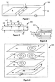
- Fig. 1 shows an element 100 according to an embodiment of the invention comprising a substrate S on a surface of which a heatable filmy structure L is drawn, the thickness h2 of which is illustrated in Fig. 2 .
- the heating element L is shown to be connected to a voltage supply V2 in order to supply electric power through a length of the element L so that the element operates as a heating resistor, the electric current heating it up.
- V2 a voltage supply
- the voltage supply may in an embodiment of the invention be also an AC supply, despite what is shown in the drawing.
- Fig. 1 shows an element 100 according to an embodiment of the invention comprising a substrate S on a surface of which a coolable filmy structure P is drawn, the thickness h3 of which is illustrated in Fig. 2 .
- the cooling element P is shown to be connected to a voltage supply V1 in order to supply electric power (V,A) through a length of the element P so that the element operates as a cooling element, the electric current cooling it down.
- V,A electric power
- the voltage supply may in an embodiment of the invention be also an AC supply, despite what is shown in the drawing.
- Fit. 1 also illustrates an embodiment of the invention where a switching and/or regulating component T, such as a thyristor, is integrated in the element P in order to regulate the electric power supplied, by regulating either the power, voltage and/or, in the case of alternating current, also the frequency and/or ignition angle.
- the regulating component T may receive its control from an external circuit such as, in the example case depicted in Fig. 6 , a car computer or a weather sensor.
- the regulating component T is shown in connection with the element P, it is obvious to a person skilled in the art, on the basis of what is presented here, that the regulating component may also be placed either alternatively or additionally in connection with the element L. Based on Fig.
- the layer thicknesses of the elements L and/or P are selected such that they will not attenuate, to a disadvantageous extent, the passing of light through the substrate, not even at spots where the element is located, even though the element is, according to an embodiment of the invention, fabricated from an opaque material in a macroscopic sense.
- Fig. 2 illustrates the film structure of the substrate S of a sheet-like element 200, without however being limited solely to a Euclidian planar object, but the substrate may also be slightly curved in an embodiment of the invention, such as in connection with an airplane wing, or more steeply curved, such as e.g. in connection with a fiber illustrated in Fig. 3 .
- the thickness h5 of the substrate S may be different in the different embodiments illustrated here, but in an embodiment in which some other sub-element, L element and/or P element are on the surface of the film, the thickness of the substrate is the thickness of the film or, depending on the case, the thickness of the layer binding together the element and the film, e.g. in connection with laminated structures.
- Fig. 2 also shows on one side of the substrate S a film K which in the example of Fig. 2 covers the element L completely and has a thickness h1.
- the film K may comprise an insulator, a photocatalytic layer, a wear-resistive surface, diamond surface, or an optically active surface.
- the L element it is possible to use the L element to produce a film which is substantially transparent on the wavelengths of visible light and ultraviolet light.
- indium, tin and/or oxides of these in the film material in an embodiment of the invention it is possible to achieve very thin films which are conductive but transparent.
- the L element it is possible to realize e.g.
- the wiring needed to operate the solar cells, to connect them in series and/or in parallel, can be achieved by an element according to an embodiment of the invention.
- the wiring is arranged for an indoor installation or alternatively for an outdoor wiring.
- said surface can be arranged so as to be heated so that it is possible to implement a defrost functionality, for instance, on the wall of a skyscraper or other building, which wall contains glass or some other transparent film arranged so as to let light pass through into the building.
- An indoor L element can also bring savings in the heating costs.
- Various display solutions may also utilize an element according to an embodiment of the invention.
- transparent wirings can be realized for a display such as a liquid crystal display.
- Even a special wiring element can be manufactured for the installation of the liquid crystal display, which wiring element is in fact on the display but, being transparent, is not visible. Thus, space can be saved inside the device.
- the surface to be coated is produced such that the surface has less than one hole per 1 mm 2 , advantageously less than one hole per cm 2 , and preferably no holes at all in the area coated.
- a hole means a hole either through the whole coating or substantially through the coating (pinhole). Holes substantially degrade the quality characteristics of the coating as well as shorten its useful life.
- the invention also pertains to a product produced this way according to the method.
- the surface coated is produced such that the first 50% of the surface is produced without particles being produced on the surface which have a diameter greater than 1000 nm, advantageously without the size of the particles exceeding 100 nm, and preferably without the size of the particles exceeding 30 nm.
- Such particles substantially degrade the quality of the coating and shorten its useful life.
- Such particles form corrosion channels in the coating.
- the invention also pertains to a product produced this way according to the method.
- the object to be coated i.e. the substrate
- AMF atomic force microscope
- the surface roughness is less than 25 nm, and preferably less than 10 nm.
- the invention also pertains to a product produced this way according to the method.
- a film designated with letters L, P the thickness of the film being h4.
- the thickness of the film P is h3, and the thickness of the film L is h2.
- the film designated with letters L, P may be an L-type heating film according to an embodiment of the invention, or a P-type cooling film according to another embodiment of the invention.
- the film may be a composite film with separate L and/or P type films arranged in laminated layers, for instance.
- Fig. 3 illustrates an embodiment of the invention in which films K, P and/or L, shown in Fig. 2 , are used on a surface of a fiber-like or tubular substrate S.
- the element 300 in Fig. 3 is shown to be cylindrical, but the invention is not limited to the cylindrical shape, but the substrate and, hence, said layers may be in a geometry according to the Figure or elliptical, for example.
- a film structure is manufactured in a geometry according to Fig. 3 , it is possible to produce e.g. a structure corresponding to a woven textile which, single- or multi-layered, may be used in filtering.
- the filter may, at least to some extent, be self-cleaning but, on the other hand, it may also be sterilized by means of a certain heat cycle. According to an embodiment of the invention it is thus possible to achieve e.g. a multi-stranded thread which can be used to weave a filter according to an embodiment of the invention, which filter can be cooled and/or heated.
- a funnel be manufactured such that on a surface thereof there is, according to an embodiment of the invention, an L and/or P type element arranged so as to produce a certain heating effect.
- Such elements may also be used, according to an embodiment of the invention, on surfaces of a vessel in order to produce a heating effect.
- the vessel may be, for example, a condenser, a container or funnel, or a transport pipe.
- Fig. 4 letters S1, S, S2, and S3 illustrate various embodiments of the invention by referring to a substrate on which the element according to the embodiment is located. Even though an embodiment of the invention in Fig. 4 can be understood to refer to an element 400 which can be realized, using the embodiments presented, as a laminated structure, the invention does not limit the elements or their numbers.
- a P-type element to produce a thermal effect which here is a cooling effect.
- the element P is drawn in the shape of a spiral in order to illustrate an advantageous shape to cover the surface and, thus, produce an even thermal effect, but, on the other hand, also to illustrate a structure in which electric power can be transmitted inductively between laminate layers from a first layer to a second layer without a galvanic contact, by means of an induction loop. It is then natural that the electric current transmitted has an amplitude, frequency and/or waveform, which can be shaped more closely according to an embodiment of the invention, e.g.
- a laminate layer contains a switching and/or regulating component by means of which it is possible to adjust the ignition angle of the alternating current (a triac).
- a triac the ignition angle of the alternating current
- the layer containing the substrate S there are both an L-type and a P-type element arranged so as to produce a thermal effect.
- the layer S can thus be used to produce both a heating-type and a cooling-type thermal effect.
- By feeding said elements independently of each other it is possible to produce simultaneous, successive or overlapping thermal effects.
- the elements L and P are drawn as separate loops in different parts of the substrate S, they can be realized as nested loops where the L and P elements travel in parallel.
- layer S2 comprising just an L element or a plurality of L elements.
- Layer S3 illustrates an embodiment of the invention in which an L or a P element realizes also an antenna, Ant, in order to transmit and/or receive a radio-frequency signal RF, represented by the arrows shown in the drawing.
- an embodiment of the invention which includes a transparent substrate, an antenna Ant, an L element and/or a P element.
- An element according to such an embodiment of the invention can be used in the windscreen of an automobile or other vehicle, a boat, train, or an aircraft, for example.
- the antenna is shown to be a part of a laminated structure on a substrate of its own, in an embodiment of the invention the antenna may also reside on one of the other substrates S1, S, and S2.
- Fig. 5 illustrates the composition of an L element and P element according to an embodiment of the invention.
- Fig. 5 also illustrates the composition of an element L1 according to an alternative composition.
- an electrically conductive filmy structure of a certain thickness is produced on a substrate by ablating at least one filmy material in order to achieve a thermal effect in the filmy structure by means of electric current.
- An element according to an embodiment of the invention has in its filmy structure a heatable part arranged as an L element.
- the heatable part may be arranged so as to be heated through electric resistance and/or inductively coupled current.
- an element comprises a first coil and a second coil, between which there is an inductive coupling in order to transfer electric power between the coils.
- One of the coils may be formed of electrical resistor material known as such at the priority date, but ablated into a film so that no wires are needed between the coils.
- an element comprises in its filmy structure a coolable part arranged as a P element.
- the coolable part may advantageously be arranged on a substrate as an integrated Peltier element which as such may be of a known type.
- a Peltier element is manufactured by ablating materials which are needed to produce the element.
- An advantage is then gained in the manufacturing in that the films produced from the materials in cold ablation according to the invention can be formed on the element substrate with a uniform quality in order to make a Peltier element, but also in a layer which is thin enough for embodiments of the invention in which the substrate is intended to function as a window or some other transparent or translucent surface.
- a vessel or condenser the temperature of which can be regulated through the thermal effect.
- a funnel according to an embodiment of the invention such that a heatable element is installed by means of ablation on a surface thereof.
- a Peltier element can be produced by means of ablation on a surface of the same or another funnel, achieving a cooling thermal effect.
- Temperature can then be used e.g. to control the growth of microbes directly on a surface of the funnel or on a filter on top of the funnel but, on the other hand, also the viscosity of the fluid, thus controlling the filtering.
- a vessel comprises a funnel part and/or a container arranged so as to collect and/or store the liquid phase of the condensed fluid produced by the cooling, the flow itself can be controlled at a certain temperature.
- the element can be used to realize a simple filmy structure or laminated filmy structure, which is essentially transparent.
- Complete transparency would require loss-free propagation of radiation at said wavelength, and cannot be achieved in practice, but a few per cent loss, such as in a normal window glass at a wavelength of visible light shall be considered transparency, and an opacity greater than e.g. 5% shall be considered substantial transparency, but on condition that the transparency is still on the order of 70%, approximately.
- a few per cent loss such as in a normal window glass at a wavelength of visible light shall be considered transparency, and an opacity greater than e.g. 5% shall be considered substantial transparency, but on condition that the transparency is still on the order of 70%, approximately.
- Persons skilled in the art are also well aware of the fact that for a window made from a given material the permeability of radiation varies as a function of the wavelength, at wavelengths outside those of visible light.
- An L element according to an embodiment of the invention has a substantial transparency at least in the wavelength range 400-700 nm.
- An L element according to an embodiment of the invention has a substantial transparency at least in the wavelength range 80-700 nm.
- An L element according to an embodiment of the invention has a substantial transparency at least at a wavelength which falls into the wavelength range 650-2000 nm.
- an L element may be used in infrared filtering, e.g. in connection with optical windows and/or components.
- a substrate coated completely on one side or where applicable, to realize structures that can filter infrared radiation For example, in military clothing, in the structural fibers of clothes, an L film can be used to achieve infrared filtering.
- an element comprises in a filmy structure a thin film and/or thick film arranged so as to vary its temperature by means of an electric current traveling through it.
- Said film may also be arranged so as to have a very small thickness in the nano-scale so that the film in some embodiments may be less than 500 nm thick, for example.
- the thickness of the film is less than 200 nm.
- the thickness of the film is less than 100 nm.
- the thickness of the film is less than 50 nm.
- the thickness of the film is less than 25 nm.
- the thickness of the film is less than 13 nm.
- the thickness of the film is less than 6 nm.
- the invention does not limit the number of films even though above a maximum film thickness is associated with a film as an example.
- one of the films may be separate from the rest of the films. In that case the film in question may be on another side of the substrate than the rest of the films.
- the films may be homogeneous in composition, both as regards the structure and the material, but not, however, limiting the invention in this respect.
- An example according to an embodiment of the invention is a film which in its material composition on a substrate comprises indium, tin and/other materials.
- the film of an L element comprises indium and tin in its composition.
- the film comprises indium and tin such that less than 90% of the mass of the film is indium.
- the film comprises indium and tin such that less than 80% of the mass of the film is indium.
- the film comprises indium and tin such that less than 70% of the mass of the film is indium.
- the film comprises indium and tin such that less than 60% of the mass of the film is indium.
- the film comprises indium and tin such that less than 50% of the mass of the film is indium. According to yet another embodiment of the invention the film comprises indium and tin such that less than 40% of the mass of the film is indium. According to yet another embodiment of the invention the film comprises indium and tin such that less than 30% of the mass of the film is indium. According to yet another embodiment of the invention the film comprises indium and tin such that less than 20% of the mass of the film is indium. According to yet another embodiment of the invention the film comprises indium and tin such that less than 10% of the mass of the film is indium.
- an L film is comprised of indium and tin in proportions given for indium in connection with the first group of embodiments, but in this other group of embodiments the indium is in the form of oxide in the film structure.
- the proportion of oxygen associated with the indium in the mass of the film is counted as indium.
- an L film is comprised of indium and tin in proportions given for indium in connection with the first group of embodiments, but in the third group of embodiments the tin is in the form of oxide in the film structure.
- the proportion of oxygen associated with the tin in the mass of the film is counted as tin.
- the film and/or the surrounding structure further contains another substance from a group of other substances in order to achieve other properties of the film structure of an element according to an embodiment of the invention in accordance with each more particular embodiment.
- a film is comprised of indium and tin in proportions given for indium in connection with the first group of embodiments, but in the fifth group of embodiments the tin is in the form of a halogen compound and/or chalcogen compound in the film structure.
- the proportion of another substance in chemical association with the tin in the mass of the film is counted as tin.
- a film is comprised of indium and tin in proportions given for indium in connection with the first group of embodiments, but in the sixth group of embodiments the tin is in the form of a halogen compound and/or chalcogen compound in the film structure.
- the proportion of another substance in chemical association with the indium in the mass of the film is counted as indium.
- an L element also comprises nickel.
- the film in the element is arranged so as to achieve a thermal effect.
- said element may also comprise an electric switch component integrated on the substrate in order to couple electric power to said electrically conductive filmy structure.
- said electric switch component comprises a FET, transistor, thyristor, diac, triac and/or a circuit comprised of those mentioned, arranged at least partly so as to couple electric power to said electrically conductive filmy structure.
- the composition of an L element is arranged such that the surface resistivity of the material thereof is less than 0.0005 ⁇ /m 2 . According to an embodiment of the invention the composition of an L element is arranged such that the surface resistivity of the material thereof is less than 0.005 ⁇ /m 2 . According to an embodiment of the invention the composition of an L element is arranged such that the surface resistivity of the material thereof is less than 0.05 ⁇ /m 2 . According to an embodiment of the invention the composition of an L element is arranged such that the surface resistivity of the material thereof is less than 0.5 ⁇ /m 2 . According to an embodiment of the invention the composition of an L element is arranged such that the surface resistivity of the material thereof is less than 5 ⁇ /m 2 .
- the composition of an L element is arranged such that the surface resistivity of the material thereof is less than 50 ⁇ /m 2 . According to an embodiment of the invention the composition of an L element is arranged such that the surface resistivity of the material thereof is less than 500 ⁇ /m 2 . According to an embodiment of the invention the composition of an L element is arranged such that the surface resistivity of the material thereof is less than 5 k ⁇ /m 2 . According to an embodiment of the invention the composition of an L element is arranged such that the surface resistivity of the material thereof is more than 5 k ⁇ /m 2 .
- said resistivity values are the resistivities of the indium-tin film of an L element according to an embodiment of the invention, whereby also other substances may be present in the films.
- at least some of the indium is replaced by nickel.
- the composition of an element according to an embodiment of the invention is adapted on the basis of the coefficient of thermal expansion of the substrate.
- an element according to an embodiment of the invention contains a material which is ablated into the film structure of the element in connection with its other materials in order to pre-set the resistivity at a certain value.
- an element according to an embodiment of the invention contains a material which is ablated into the film structure of the element in connection with its other materials in order to pre-set the coefficient of thermal expansion at a certain value for the substrate.
- said material is an additive of an indium-tin film, whereby other materials, too, may be present in the film.
- An element according to an embodiment of the invention is arranged such that it has an antenna structure and/or a means for using an electrically conductive filmy structure as an antenna and/or part thereof.
- the antenna may be one of the following: transmitter antenna, receiver antenna, or a combination of the two. More particularly the antenna may be designed in accordance with the special characteristics of its embodiment so as to function as a GPS antenna, mobile station antenna, radio antenna, TV antenna, an antenna for the transmission/reception of a digital signal and/or an analog signal.
- an inductive loop or a similar coil may function as some kind of a helix antenna at the same time as it can function as an element for producing a thermal effect.
- an element may comprise in addition to a first film structure also a second film structure in order to achieve a first thermal effect and a second thermal effect. This is illustrated by an example depicted in Fig. 4 . These thermal effects may be different, occur at different times, and/or be directed to different sides of the substrate ( Fig. 2 ), not, however, being limited to these.
- said first film structure in an element is arranged so as to be an L element for increasing the temperature
- said second film structure is arranged so as to be a P element for decreasing the temperature.
- an element may further include an antenna structure as a partial element in accordance with an embodiment of the invention.
- an element contains a plurality of film structures, it can be manufactured according to an embodiment of the invention in such a manner that it has a film structure integrated on a surface of a part of a substrate, whereby said element is one of a group of similarly formed elements, e.g. layered in a laminate form according to Fig. 4 but not, however, being limited solely thereto.
- Lamination can be used to prevent the electrically conductive layers/parts from directly touching each other. If, for example, a layer includes tin and/or indium e.g. in a heatable element (substrates S and S2), but there is a Peltier element formed in another layer (substrates S and S1), a direct contact between the layers can then be avoided if necessary.
- the heatable element can be made resistive (L element in Fig. 1 ), i.e. a thermal resistor complying with Ohm's law, but in another embodiment of the invention it may be designed so as to function inductively ( Fig. 4 depicts both inductive and ohmic) but also according to the eddy current principle.
- the substrate is a planar substrate.
- the substrate may also be a cylinder, even a thread or a fiber.
- the substrate of the element is one of the following: plastic, paper, textile, fabric, glass, ceramic, stone, metal, pigment or a combination of any of the above.
- the element and the substrate constitute a film that can be bent.
- the film, which can be bent is arranged so as to be adhesively attached to its substrate.
- the thermal effect can be achieved through an element arranged on the surface of such a fiber, whereby the fiber can be used as a part of a web-like structure, for instance.
- one such web-like structure is arranged for the purpose of filtration so as to produce a thermal effect in connection with the filtering, for pre- and/or post-optimization of the filtering from the point of view of the properties of the material to be filtered. It is then advantageous if e.g. either the outermost or the next-to-outermost surface on the fiber is electrically insulated.
- the outermost or next-to-outermost surface of the fiber of said kind may comprise a photocatalyst for breaking down organic matter.
- bacterial growth can be kept down by cooling the filter and/or the funnel holding the filter so that a photocatalyst enables the breaking down of bacterial matter by means of light.
- the filter may also be at a high temperature to kill microbes.
- the filter and/or its holder may also be cooled and heated cyclically. The cycles may be equal or unequal in length, the cooling cycles with each other or the heating and cooling cycles alternating. Heating and/or cooling may also be utilized to keep the temperature of the element at a certain value.
- One application for an element according to an embodiment of the invention is e.g. to be a part of a radar antenna in a radar of a craft designed to travel on ground, at sea and/or in the air.
- a fixed radar can utilize applicable embodiments of the invention.
- a thermal effect can be achieved e.g. for a part of a vehicle, where applicable.
- a thermal effect may be directed onto a surface of an airplane, flying boat, ship or some other watercraft, whereby the surface may be a part of a stabilizer, rudder, wing and/or hull.
- the vehicle may then be e.g. one of the following: boat, ship, submarine, car, truck, bus, railway carriage, engine, trolley bus, tram, subway carriage, airship, balloon, helicopter, airplane, parachute, other air vehicle.
- a vehicle also refers, where applicable, to vehicles designed for military transport and/or battle duties, such as personnel transport vehicles and battle tanks.
- a military vehicle can be camouflaged in winter conditions using atmospheric water vapor which is nucleated and/or condensed and, hence, crystallized.
- atmospheric water vapor which is nucleated and/or condensed and, hence, crystallized.
- the beginning of nucleation and condensation can be made quicker in sub-zero temperatures, but also in higher temperatures in a manner depending on the cooling power of the P element.
- ice, frost or moisture is to be removed from a surface of a military vehicle, it can be achieved using an appropriately designed L element.
- said military vehicle is a so-called dummy which is towed, drawn and/or radio-controlled at a distance from a more important target - such as an expensive stealth-coated armored vehicle - with the purpose of drawing enemy fire to the dummy instead of the real target.
- a P element for example, in the surface structure of the dummy, an ice/water coating can be produced on the dummy, which can be visible in certain radar applications so that it is assumable that the enemy will fire at the visible target, thereby increasing the survival chances of the military vehicle proper under fire.
- a dummy is arranged, by means of an L element, so as to be especially well visible in the infrared range.
- Figs. 6 to 9 illustrate examples of use of an element according to an embodiment of the invention, using various vehicles as examples.
- the element is used in connection with a vehicle.
- the thick line is intended to emphasize the windscreen and/or rear window, as well as the side window, of the vehicle, also other parts of the vehicle may serve as substrates (S) for L and/or P type elements, but an element comprising antenna functions is best suited for non-metallic parts, especially windows.
- an element according to an embodiment of the invention can also be used e.g. in skylight windows both in automobiles and in buildings, but also in greenhouses.
- Globes of lamps can be equipped with elements according to an embodiment of the invention for the purpose of heating/cooling them.
- the headlights of a vehicle can be kept free of ice/slush/snow in winter conditions by heating the surfaces of the lighting equipment by means of an L element, for instance.
- the substrate S is a part of a hot-air balloon to illustrate the use of an element according to an embodiment of the invention in order to achieve a thermal effect directed to an aircraft 700. It is true that by producing enough electricity it is possible in an aircraft, in a period of time long enough, use an element on a substrate S to control the weight of the air vehicle e.g. by means of water condensed on the element. However, in an embodiment of the invention for producing sufficient condensation for weight control purposes for a large air vehicle solely by means of condensation, using Peltier elements known at the priority date of the present invention, the efficiency of such elements may not be sufficient for achieving a significant weight increase exclusively by cooling.
- P elements which are arranged to be selectable, so that by choosing certain ones from a large number of P elements the temperature in each can be dropped sufficiently to start nucleation, whereby, using elements small enough, nucleation and, hence, formation of ice can be controlled by controlling the elements in operation. Placement of P and/or L elements can also contribute to the stability control of an aircraft.
- optically visible layers can be produced by means of p elements by combining condensation and lighting, e.g. to achieve an advertisement, on the outer and/or inner surface of a hot-air balloon or some other aircraft, for instance.
- Fig. 8 illustrates an airplane, its wing surface, surface of the rudder and/or windscreen, where it is possible to use e.g. an L type element to achieve heating and, thus, reduce ice formation.
- the substrate S may also be the fuselage of the plane, for example.
- Fig. 9 shows a triplane, it is obvious to a person skilled in the art that an element according to an embodiment of the invention can also be used in modem passenger, fighter and/or training planes, but also in helicopters. It is further noted that an element according to an embodiment of the invention can be used in the manufacture of a spaceship, as a part thereof.
- Fig. 9 illustrates the use of an element in connection with a watercraft. Even though the thicker line in the drawing emphasizes the use of the element in the windshield of a boat, it is obvious to a person skilled in the art that other surfaces, too, may serve as locations for the element.
- a boat is just an example of a watercraft, which also includes various submarines and/or diving bells, amphibious vehicles, ships, catamarans, various surfaces in sailboats, and also flying boats. Furthermore, it is possible to reduce fogginess in a diver's mask using the element in the transparent part of the mask as long as enough electrical power is provided in order to achieve a thermal effect.
- An element may also be used on a surface of a building or such, illustrated in Fig. 10 .
- An element may also be used to create an advertising surface, referring to the text "commercial area” on the twin towers, whereas the letters "ms" refer to a work of art for the technical realization of which the element or group of elements can be used. Then, by means of the thermal effect, e.g. in summer and/or winter conditions, it is possible to achieve, through a change in the liquid phase, changing surfaces which can be lighted in order to create artistic effects by means of said technology. Indeed, one of the uses of the element is on advertising surfaces or surfaces of certain objects.
- the surface onto which the thermal effect is directed may also be more specifically arranged on the basis of the film structure of the element in such a manner that said surface is adapted so as to produce patterns through refracted/reflected light, with the help of the gas sublimated from the fluid which is condensed as a consequence of the thermal effect and/or at least one optical element formed of particles therein.
- the surface may be one of a group of surfaces which are each separately adapted so as to take into consideration the properties of the condensing fluid.
- One use of the invention is such that a P element is used to produce a structure on an outer surface of which it is to be condensed a component, e.g. water, of the gas phase which envelopes said surface. Then in a suitable closed space the water will be condensed on the surface cooled by the P element so that elsewhere, i.e. other than in the immediate vicinity of the P element, the proportion of water vapor in the gas phase is reduced, which improves the operating reliability of an electric appliance, for example.
- a component e.g. water
- the surface with which the surface according to an embodiment of the invention is arranged by means of a film structure may also comprise two separate surfaces.
- the surface may also be a window surface and/or decorative surface for which a thermal effect can be achieved when there is an element according to an embodiment of the invention on the surface.
- the element is integrated as a fixed part of the surface through ablation already in the manufacturing stage.
- the element is later integrated in the surface in a fixed manner, but only after the manufacture of the surface, by means of ablation.
- the element is on a film which can be glued or otherwise adhered to a window of a building or an automobile, just to name a couple of examples.
- an element according to an embodiment of the invention can be fabricated on a surface of a substrate by ablation.
- the method includes a step of ablating a first film material 1101 and/or a second film material 1102 in order to achieve an electrically conductive filmy structure.
- the method advantageously includes a step in which at least one film material is selected to be ablated so that a certain thermal effect can be produced on the finished element.
- Fig. 11 does not show the selection step as such, but it is illustrated using a broken line in connection with step 1102.
- a jet of ablated film material is conducted 1103 onto a substrate onto which the material adheres/is attached 1104 formed into a film in a certain manner depending on the intended use of the element.
- an element manufacturing equipment includes a means of ablation for ablating a film material from an ablation target, a means for directing 1103 a jet of ablated film material onto a substrate to produce a film structure, a heating means for pre-heating 1105 the substrate and/or ablation target to improve ablation and/or adhesion.
- said ablation means comprises a laser source.
- said laser source comprises a picosecond laser, femtosecond laser and/or an attosecond laser.
- different lasers can also be used in pre-heating the material to be ablated, in heating the substrate to be coated. It is also possible to use different lasers for different film materials.
- a first laser is used for a first film material, which has a first repetition frequency, a first radiation wavelength, a first pulse length and/or a first intensity, arranged so as to ablate a first film material.
- a second laser is used for a second film material, which has a second repetition frequency, a second radiation wavelength, a second pulse length and/or a second intensity, arranged so as to ablate a second film material.
- a manufacturing equipment comprises in connection with said ablation means a radiation transmission line for laser radiation.
- a radiation transmission line for laser radiation includes a turbine scanner for laser radiation.
- the repetition frequency of the ablation means for a manufacturing equipment is less than 5 MHz but over 1 MHz.
- the repetition frequency is more than 5 MHz but less than 20 MHz.
- the repetition frequency is more than 15 MHz but advantageously less than 30 MHz.
- the repetition frequency is more than 25 MHz but less than 60 MHz.
- the repetition frequency is more than 40 MHz but less than 100 MHz.
- the upper limit for the repetition frequency is actually determined by the mechanical strength of the turbine scanner parts changing the direction of propagation of radiation, considering the effects of the rotating speed, so that by using a suitably strong material it is possible to achieve higher repetition frequencies without the turbine scanner breaking down because of the speed of revolution and/or bearing tolerances.
- the manufacture of the film structures of the element itself is arranged to take place within a protective gas atmosphere and/or vacuum in order to achieve sufficient purity, to which end the manufacturing equipment according to an embodiment of the invention comprises a vacuum means and/or protective gas means adapted for the coating of an element.
- the film of the element can be manufactured directly from source materials through ablation. Then it is also possible to use a reactive protective gas to achieve a certain composition of a suitable film material compound.
- the film of an L element is fabricated from pure indium and/or tin in an oxygen atmosphere, in conditions in which the film material is formed on the substrate when ablated indium and oxygen react with each other and/or ablated tin and oxygen react with each other.
- a manufacturing equipment includes a radiation shield for deceleration and/or other radiation for absorbing the radiation generated by an electric charge in accelerating motion.
- a manufacturing equipment includes a fume cupboard, desiccator and/or cycling and extraction means for materials present in the exhaust gases, comprised of surplus matter and freed in the manufacture of the element.
- an element according to an embodiment of the invention can be used to produce a window structure according to an embodiment of the invention so that a thermal effect can be achieved by the element in said window structure.
- the window structure includes a first sub-layer and a second sub-layer so that said first sub-layer is isolated from said second sub-layer, but said first sub-layer comprises an element according to an embodiment of the invention arranged in the form of a first coil, and said second sub-layer comprises an element according to an embodiment of the invention arranged in the form of a second coil for inductively supplying electric power to said first coil.
- the thermal effect achieved is one of the following: heating, cooling, holding the temperature, alternation of heating and cooling.
- Pulse energy refers to the total energy of one pulse, focused onto a desired area through optical components.
- a laser jet was focused onto a spot with a diameter of 13.6 to 20 micrometers.
- the fluence (pulse energy/area) was varied typically between 0.3 and 5.6 J/cm2.
- the wavelength used in the coating processes was 1064 nm. Since coatings were made with different coating distances and powers and without growing films of different thickness for the different tests, the coating times varied from a few minutes to three hours.
- nominal laser power One should understand that part of this nominal power is lost partly in various power losses when the pulse optically travels to the surface of the target. Such power losses occur e.g. in lenses and optical fiber.
- a glass plate was coated (Pilkington, 3 to 5-mm thick glasses of different types, pure, cladding glass, tinted glass, activ glass) with indium-tin oxide (In 2 O 3 :SnO 2 , 9:1, Sigma Technology, China).
- indium-tin oxide In 2 O 3 :SnO 2 , 9:1, Sigma Technology, China.
- pieces of silicon laboratory glass (2 mm thick, 2 cm x 3 cm piece of boron silicate glass), SS (stainless steel), copper, marble plate and plastic backgrounds (PC, Kapton, Mylar). Sizes of the latter samples varied from 1x1 cm2 to 10x10 cm2 with a thickness of 0.1 to 10 mm.
- the parameters of the laser equipment were as follows:
- the resulting indium-tin oxide surface was examined with an atomic force microscope (AFM), optical microscope, and ESEM microscope.
- the thickness of the indium-tin oxide surface varied in the test series between 50 and 500 nm and the evenness of the surface ⁇ 0.3 to 5 nm measured from an area of 1 ⁇ m 2 . No microparticles were detected on the surface.
- the ITO-coated glass was optically fully transparent. Adhesion of the coating was good, and it was initially tested using the tape test and by scratching. No holes were detected on the coating.
- an indium-tin-oxide-coated piece of glass was coated with aluminum-titanium oxide in order to produce a hard, so-called scratch-free coating on top of the indium-tin oxide surface.
- a fluence of 0.5 to 0.8 J/cm2 was used in the aluminum-titanium oxide coating.
- the parameters of the laser equipment were as follows:
- the resulting aluminum-titanium oxide surface was examined with an atomic force microscope (AFM) and ESEM microscope.
- the thickness of the resulting surface varied in the test samples between 50 and 400 nm and the evenness of the surface was under ⁇ 10 nm measured from an area of 1 ⁇ m 2 . No microparticles were detected on the surface.
- a piece of glass coated in the manner depicted in Fig. 1 was further coated with yttrium-stabilized zirconium oxide in order to produce a hard, so-called scratch-free coating on top of the indium-tin oxide surface.
- a fluence of 0.5 to 1.0 J/cm2 was used in the Y-ZrO2 oxide coating.
- the parameters of the laser equipment were as follows:
- the resulting zirconium oxide surface was examined with an atomic force microscope (AFM) and ESEM microscope.
- the thickness of the resulting surface varied between 100 and 300 nm, approximately, and the evenness of the surface ⁇ 2 nm measured from an area of 1 ⁇ m 2 . No microparticles were detected on the surface.
- the final piece of glass with an ITO coating and a zirconium oxide coating on top of that was optically transparent. Based on scratch tests and pin-on-disk tests, the abrasion resistance of a structure coated with the oxide was significantly better than without the oxide coating.
- a sheet-form piece of glass and polycarbonate (3 cm x 3 cm, thickness 1.2 mm) was coated with indium-tin oxide in such a manner that an indium-tin alloy was ablated with laser in a reactive oxygen phase.
- the chamber was pumped into a pressure of about 10 -5 mbar.
- the pumping was suitably throttled by means of a check valve before letting the reactive gas in.
- the pressure of the oxygen gas was regulated according to a vacuum gauge typically from 10 -4 to 10 -1 mbar by means of a gas supply valve.
- the laser dose was controlled such that at each gas pressure the ablation threshold was reached and a stable ablation stage was achieved where the target would no more excessively spark and no macro-particles would visibly come off it.
- the parameters of the laser equipment were as follows:
- the resulting indium-tin oxide surface was examined with an atomic force microscope (AFM) and ESEM microscope.
- the thickness of the indium-tin oxide surface was between 50 and 100 nm, approximately, and the evenness of the surface ⁇ 1 nm measured from an area of 1 ⁇ m 2 . No microparticles were detected on the surface. Adhesion of the coating was good, and it was initially tested using the tape test and by scratching. Conductivity of the surfaces produced was initially tested using surface measurement with an accurate multimeter (Fluke 189). The surfaces appeared to be conductive, behaving just like ITO surfaces produced by other methods and tested in a similar manner.
- a steel object was coated with a titanium oxide coating.
- the parameters of the laser equipment were as follows, and the surface was produced by ablating titanium in a helium atmosphere containing oxygen. Tests were conducted at different gas pressures with the vacuum total pressure varying between 0.5 and 10 -2 mbar according to a vacuum gauge.
- the resulting titanium oxide surface was examined with an atomic force microscope (AFM), optical microscope, and ESEM microscope.
- the thickness of the titanium oxide surface was about 50 nm, and the evenness of the surface ⁇ 3 nm measured from an area of 1 ⁇ m 2 .
- the films appeared to be equivalent to similar films fabricated by us by means of ablation from a TiO 2 source.
- a slab of marble (100 mm - 100 mm) was coated by ablating an indium-tin metal target (9:1) in active oxygen, 10 -4 to 10 -1 mbar.
- the pulse frequency used was 4 MHz, pulse length 5 ⁇ J, and pulse length 20 ps.
- the distance between the target and the substrate was 35 mm.
- the vacuum level was 10 -5 atm before supplying the active gas.
- the method resulted in a continuous, transparent and hole-free coating with a thickness of 100 nm approximately. Surface roughness was measured to be less than 3 nm from an area of 1 ⁇ m2 (AFM). Electrical resistance was measured to be 2.2 x 10 -3 ⁇ /m 2 .
- a piece of a sheet of copy paper (80 g/m 2 , 100 mm x 100 mm) was coated by ablating an ITO in oxide form (90 w-% In 2 O 3 ; 10 w-% SnO 2 ) at a pulse frequency of 3 MHz while the pulse energy was 5 ⁇ J and the pulse length 20 ps.
- the distance between the target and the substrate was 40 mm.
- the vacuum level was 10 -6 atm during the coating process.
- the process produced a continuous, transparent coating.
- the thickness of the coating was 570 nm.
- Fig. 13 illustrates an example of a deposition of an ITO coating (Indium-Tin-Oxide) on a piece of polycarbonate sheet ( ⁇ 100 mm x 30 mm) using an optical scanner according to the prior art, namely an oscillating (galvano-scanner) for different ITO thin film thicknesses (30 nm, 60 nm, and 90 nm).
- Fig. 13 clearly demonstrates the drawbacks associated to oscillating mirror solutions used as optical scanner especially with ultra-short pulse laser deposition (USPLD) but also in laser-assisted coating in general.
- ITO coating Indium-Tin-Oxide
- USPLD ultra-short pulse laser deposition
- the angular velocity of the mirror is not constant in the vicinity of an end point of the movement. Because of the oscillating movement, the mirror constantly has to decelerate and stop before accelerating again, thus resulting in uneven target treatment at the fringes of the scanning area. This, in turn, results in poor quality plasma, which may also include particles especially at the fringes of the scanning area, eventually leading to an uneven coating result like that shown in the Figure.
- the deposition parameters in this example are chosen so as to demonstrate the uneven distribution with the ablated matter so as to make clear the nature of the scanner. If, however, the same scanner is used and the parameters are appropriately chosen so as to improve the quality of the film, the problems become invisible to the naked eye, but are not, however, eliminated.
- An element according to an embodiment of the invention comprises an electrically conductive filmy structure of a certain thickness produced on a substrate by ablating, with high-quality plasma, at least one film material in order to achieve a thermal effect in the filmy structure by means of electric current.
- the element comprises a heatable part in the filmy structure.
- the heatable part is arranged so as to be heated through electrical resistance and/or inductively coupled current.
- the element comprises a coolable part in the filmy structure.
- the coolable part is arranged so as to be a Peltier element integrated on a substrate.
- said element in said element it comprises a funnel part and/or a container arranged so as to collect and/or store the liquid phase of the condensed fluid produced by the cooling, at a certain temperature.
- said element comprise the filmy structure thar is substantially transparent.
- the element comprises in a filmy structure a thin film and/or thick film arranged so as to vary its temperature by means of an electric current traveling through it.
- said film thickness is less than 100 nm. According to an embodiment of the invention in said element said film thickness is less than 50 nm. According to an embodiment of the invention in said element said film thickness is less than 25 nm. According to an embodiment of the invention in said element said film thickness is less than 13 nm.
- said element further comprises integrated on a substrate an electrical switch component for coupling electric power to the electrically conductive filmy structure.
- the electric switch component comprises a FET, transistor, thyristor, diac, triac and/or a circuit comprised of those mentioned, arranged at least partly so as to couple electric power to the electrically conductive filmy structure.
- the antenna is one of the following: transmitter antenna, receiver antenna, or a combination of the two.
- the antenna comprises one of the following: a GPS antenna, a mobile phone antenna, a radio antenna, a TV antenna, an antenna for transmitting/receiving a digital signal and/or an analog signal.
- the element comprises a first film structure and a second film structure for achieving a first thermal effect and for achieving a second thermal effect.
- said first film structure is arranged so as to raise the temperature and said second film structure is arranged so as to drop the temperature.
- the element further comprises an antenna structure.
- an element according to an embodiment of the invention has a laminated structure so that that the element has a filmy structure integrated on the surface of a part of a substrate, whereby the element is one of a group of other similarly formed elements layered as a laminate.
- the element according to an embodiment of the invention contains tin as one constituent in the filmy structure.
- the element according to an embodiment of the invention contains indium as one constituent in the filmy structure.
- the element according to an embodiment contains bismuth as one constituent in the filmy structure.
- an element according to an embodiment of the invention has got a resistance from a filmy material composed of indium and tin.
- the substrate of the element is one of the following: plastic, paper, textile, fabric, glass, ceramic, stone, metal, pigment or a combination of any of the above.
- the element and the substrate constitute a bendable film.
- the element is arranged on a surface of a fiber to achieve a web-like structure.
- the element is is arranged on a surface of a fiber to achieve a thermal effect in a filter structure.
- the outermost or next-to-outermost surface of said fiber is electrically insulated.
- the outermost or next-to-outermost surface of said fiber comprises a photo-catalyst for breaking down organic substances.
- the use of an element according to an embodiment of the invention comprises such a use to achieve a thermal effect on a surface, when the element is an element according to an embodiment.
- Use of an element according to an embodiment of the invention comprises use for such a thermal effect which means raising a temperature.
- Use of an element according to an embodiment of the invention comprises use for such a use in which the thermal effect means sustaining a temperature which has been set.
- Use of an element according to an embodiment of the invention comprises use for such a use in which the thermal effect means decreasing a temperature.
- Use of an element according to an embodiment of the invention comprises use for such a use in which the surface is a part of a stabilizer, rudder, wing and/or hull.
- Use of an element according to an embodiment of the invention comprises use for such a use in which the surface is a part of an antenna of a radar.
- Use of an element according to an embodiment of the invention comprises use for such a use in which the surface is a part of a vehicle.
- Use of an element according to an embodiment of the invention comprises use for such a use in which the vehicle is one of the following: boat, ship, submarine, car, truck, bus, railway carriage, engine, trolley bus, tram, subway carriage, airship, balloon, helicopter, airplane, parachute, other air vehicle.
- Use of an element according to an embodiment of the invention comprises use for such a use in which the surface is a surface of a part of a building.
- Use of an element according to an embodiment of the invention comprises use for such a use in which the surface is an advertising surface.
- Use of an element according to an embodiment of the invention comprises use for such a use in which the surface is a surface of a changing work of art.
- Use of an element according to an embodiment of the invention comprises use for such a use in which the surface is adapted so as to produce patterns through refracted/reflected light with the help of a gas sublimated from the liquid which is condensed as a consequence of the thermal effect and/or by means of at least one optical element formed of particles formed from it.
- Use of an element according to an embodiment of the invention comprises use for such a use in which the surface is one of a group of surfaces which are each separately arranged the liquid condensed.
- Use of an element according to an embodiment of the invention comprises use for such a use in which the group comprises at least two different surfaces.
- Use of an element according to an embodiment of the invention comprises use for such a use in which the surface is a window surface.
- Use of an element according to an embodiment of the invention comprises use for such a use in which the surface is a decorative surface.
- Use of an element according to an embodiment of the invention comprises use for such a use in which the method includes a step for ablating, to produce a high-quality plasma, a first film material and/or a second film material to achieve an electrically conductive filmy structure.
- Use of an element according to an embodiment of the invention comprises use for such a use in which the method includes a step in which at least one film material is selected to be ablated in order to achieve a certain thermal effect for the finished element.
- a surface-treatment equipment according to an embodiment of the invention has in its radiation transmission line a turbine scanner for working and/or coating a work-piece using high-quality plasma.
- a method for manufacturing an element according to an embodiment of the invention comprises in the method, in addition to ablating a film material from an ablation target to produce high-quality plasma, directing a jet of the film matter onto the substrate of the element to produce a film structure, and pre-heating the substrate and/or the ablation spot on the ablation target, in order to improve ablation and/or adhesion on the substrate.
- An element manufacturing equipment includes a means of ablation for ablating a film material from an ablation target to produce high-quality plasma, a means for directing a jet of ablated film matter onto the substrate of the element to produce a film structure, a heating means for pre-heating the substrate and/or ablation target to improve ablation and/or adhesion.
- An element manufacturing equipment is so arragned that said ablation means comprises a laser source for producing high-quality plasma.
- An element manufacturing equipment according to an embodiment of the invention comprises in said element manufacturing equipment said laser source which comprises a picosecond laser, femtosecond laser and/or attosecond laser for producing high-quality plasma.
- An element manufacturing equipment is so arranged that in said element manufacturing equipment said ablation means comprises a radiation transmission line for laser radiation for producing high-quality plasma.
- An element manufacturing equipment is so arranged that in said element manufacturing equipment said ablation means comprises in a radiation transmission line a turbine scanner for laser radiation for producing high-quality plasma.
- An element manufacturing equipment is so arranged that in said element manufacturing equipment the ablation means is arranged to have a repetition frequency in excess of 30 MHz, advantageously over 60 MHz, but preferably over 100 MHz for producing high-quality plasma.
- An element manufacturing equipment comprises a vacuum means and/or protective gas means for coating an element, arranged so as to produce high-quality plasma.
- An element manufacturing equipment comprises a radiation shield for deceleration radiation for producing high-quality plasma.
- An element manufacturing equipment comprises a fume cupboard, desiccator and/or cycling and storage means for the surplus material present in the exhaust gases freed in the manufacture of an element, for the purpose of producing high-quality plasma.
- a window structure according to an embodiment of the invention comprises an element according to an embodiment of the invention for producing a thermal effect.
- a window structure according to an embodiment of the invention includes a first sub-layer and a second sub-layer so that said first sub-layer is isolated from said second sub-layer, but said first sub-layer comprises an element according to an embodiment of the invention as arranged in the form of a first coil, and said second sub-layer comprises an element according to an embodiment of the invention as arranged in the form of a second coil for inductively supplying electric power to said first coil.
- a window structure according to an embodiment of the invention is so arranged that the thermal effect for said window structure is one of the following: heating, cooling, holding the temperature, alternation of heating and cooling.
Landscapes
- Engineering & Computer Science (AREA)
- Physics & Mathematics (AREA)
- Optics & Photonics (AREA)
- Mechanical Engineering (AREA)
- Chemical & Material Sciences (AREA)
- Plasma & Fusion (AREA)
- Metallurgy (AREA)
- Toxicology (AREA)
- Chemical Kinetics & Catalysis (AREA)
- Materials Engineering (AREA)
- Health & Medical Sciences (AREA)
- Organic Chemistry (AREA)
- Manufacturing & Machinery (AREA)
- Electromagnetism (AREA)
- Physical Vapour Deposition (AREA)
- Physical Or Chemical Processes And Apparatus (AREA)
- Details Of Aerials (AREA)
- Thin Film Transistor (AREA)
- Apparatuses And Processes For Manufacturing Resistors (AREA)
- Bipolar Transistors (AREA)
- Laser Beam Processing (AREA)
- Surface Heating Bodies (AREA)
Applications Claiming Priority (4)
| Application Number | Priority Date | Filing Date | Title |
|---|---|---|---|
| FI20060177A FI20060177A7 (fi) | 2006-02-23 | 2006-02-23 | Menetelmä tuottaa hyvälaatuisia pintoja ja hyvälaatuisen pinnan omaava tuote |
| FI20060182A FI20060182A7 (fi) | 2005-07-13 | 2006-02-23 | Ablaatiotekniikkaan liittyvä pinnankäsittelytekniikka ja pinnankäsittelylaitteisto |
| FI20060357A FI124239B (fi) | 2006-02-23 | 2006-04-12 | Elementti, jossa on sähköä johtava kalvomainen rakenne lämmittävän ja/tai jäähdyttävän vaikutuksen synnyttämiseksi sähkövirran avulla |
| PCT/FI2007/000048 WO2007096463A2 (en) | 2006-02-23 | 2007-02-23 | Element |
Publications (2)
| Publication Number | Publication Date |
|---|---|
| EP1991716A2 EP1991716A2 (en) | 2008-11-19 |
| EP1991716B1 true EP1991716B1 (en) | 2011-09-21 |
Family
ID=36293753
Family Applications (1)
| Application Number | Title | Priority Date | Filing Date |
|---|---|---|---|
| EP07712590A Not-in-force EP1991716B1 (en) | 2006-02-23 | 2007-02-23 | Element |
Country Status (7)
| Country | Link |
|---|---|
| EP (1) | EP1991716B1 (https=) |
| JP (1) | JP5383204B2 (https=) |
| KR (1) | KR20090015021A (https=) |
| AT (1) | ATE525493T1 (https=) |
| DK (1) | DK1991716T3 (https=) |
| FI (1) | FI124239B (https=) |
| WO (1) | WO2007096463A2 (https=) |
Cited By (1)
| Publication number | Priority date | Publication date | Assignee | Title |
|---|---|---|---|---|
| CN102509830A (zh) * | 2011-10-25 | 2012-06-20 | 长春理工大学 | 一种含有飞秒激光等离子体丝的双线传输线装置 |
Families Citing this family (12)
| Publication number | Priority date | Publication date | Assignee | Title |
|---|---|---|---|---|
| KR101706517B1 (ko) * | 2011-01-13 | 2017-02-13 | 타마랙 사이언티픽 컴퍼니 인코포레이티드 | 전도성 시드 레이어를 레이저 제거하는 방법 및 장치 |
| JP4782897B1 (ja) * | 2011-04-11 | 2011-09-28 | 隆彌 渡邊 | 冷暖房装置 |
| JP4856282B1 (ja) * | 2011-07-30 | 2012-01-18 | 隆彌 渡邊 | 冷暖房装置 |
| WO2012140800A1 (ja) * | 2011-04-11 | 2012-10-18 | Watanabe Takaya | 冷暖房装置 |
| JP4791611B1 (ja) * | 2011-05-20 | 2011-10-12 | 隆彌 渡邊 | 冷暖房装置 |
| CN106487323A (zh) * | 2015-08-26 | 2017-03-08 | 阿特斯(中国)投资有限公司 | 光伏组件安装系统 |
| CN109583110A (zh) * | 2018-12-06 | 2019-04-05 | 东北大学 | 一种冶金过程的放大方法 |
| CN110308070A (zh) * | 2019-06-18 | 2019-10-08 | 东南大学 | 一种采用3d打印的气体扩散室 |
| CN112098711B (zh) * | 2020-09-24 | 2024-01-23 | 中国人民解放军63920部队 | 基于稀疏遥测的月球车帆板功率衰减确定方法及装置 |
| CN112556018B (zh) * | 2020-12-14 | 2022-04-29 | 珠海格力电器股份有限公司 | 一种自清洁过滤网及空调 |
| CN113049911B (zh) * | 2021-03-10 | 2022-12-06 | 杭州惠嘉信息科技有限公司 | 一种太阳能输电电路监测系统及其监控方法 |
| DE102024117849A1 (de) | 2024-06-25 | 2026-01-08 | Marelli Germany Gmbh | Kraftfahrzeugbeleuchtungseinrichtung mit einer beheizbaren Abdeckscheibe |
Family Cites Families (21)
| Publication number | Priority date | Publication date | Assignee | Title |
|---|---|---|---|---|
| JPH0791660B2 (ja) * | 1989-08-30 | 1995-10-04 | 株式会社日立製作所 | 環境遮断用耐熱壁を備えた地上機器 |
| JPH03114467U (https=) * | 1990-03-09 | 1991-11-25 | ||
| DE4019965A1 (de) * | 1990-06-21 | 1992-01-09 | Deutsche Forsch Luft Raumfahrt | Verfahren und vorrichtung zum beschichten von substratmaterial |
| JP3255469B2 (ja) * | 1992-11-30 | 2002-02-12 | 三菱電機株式会社 | レーザ薄膜形成装置 |
| JPH06248440A (ja) * | 1993-02-26 | 1994-09-06 | Kokusai Chodendo Sangyo Gijutsu Kenkyu Center | 酸化物薄膜作製装置 |
| US5368681A (en) * | 1993-06-09 | 1994-11-29 | Hong Kong University Of Science | Method for the deposition of diamond on a substrate |
| US5652062A (en) * | 1993-10-27 | 1997-07-29 | Lucent Technologies Inc. | Devices using transparent conductive GaInO3 films |
| US5624722A (en) * | 1995-03-07 | 1997-04-29 | Sumitomo Electric Industries, Ltd. | Apparatus and method for depositing films on substrate via on-axis laser ablation |
| US6063455A (en) | 1995-10-09 | 2000-05-16 | Institute For Advanced Engineering | Apparatus for manufacturing diamond film having a large area and method thereof |
| JPH1032166A (ja) * | 1996-07-16 | 1998-02-03 | Toyota Motor Corp | レーザーアブレーション法による結晶薄膜の形成方法 |
| AUPO912797A0 (en) * | 1997-09-11 | 1997-10-02 | Australian National University, The | Ultrafast laser deposition method |
| AU6431199A (en) | 1998-10-12 | 2000-05-01 | Regents Of The University Of California, The | Laser deposition of thin films |
| AU2514900A (en) * | 1999-01-27 | 2000-08-18 | United States Of America As Represented By The Secretary Of The Navy, The | Fabrication of conductive/non-conductive nanocomposites by laser evaporation |
| JP2001140059A (ja) * | 1999-11-12 | 2001-05-22 | Natl Research Inst For Metals Ministry Of Education Culture Sports Science & Technology | レーザー蒸着成膜方法 |
| JP2001266646A (ja) * | 2000-03-16 | 2001-09-28 | Matsushita Electric Ind Co Ltd | 誘電体複合薄膜とその応用素子 |
| JP4621333B2 (ja) * | 2000-06-01 | 2011-01-26 | ホーチキ株式会社 | 薄膜形成方法 |
| JP2002294431A (ja) * | 2001-04-02 | 2002-10-09 | Sony Corp | 成膜方法 |
| JP2003109434A (ja) * | 2001-06-27 | 2003-04-11 | Bridgestone Corp | 透明導電フィルム及びタッチパネル |
| JP4894103B2 (ja) * | 2001-07-24 | 2012-03-14 | 株式会社ブリヂストン | 透明導電フィルム及びタッチパネル |
| CA2469500A1 (en) * | 2001-12-21 | 2003-07-10 | Ifire Technology Inc. | Method of laser ablation for patterning thin film layers for electroluminescent displays |
| US7879410B2 (en) * | 2004-06-09 | 2011-02-01 | Imra America, Inc. | Method of fabricating an electrochemical device using ultrafast pulsed laser deposition |
-
2006
- 2006-04-12 FI FI20060357A patent/FI124239B/fi not_active IP Right Cessation
-
2007
- 2007-02-23 JP JP2008555815A patent/JP5383204B2/ja not_active Expired - Fee Related
- 2007-02-23 EP EP07712590A patent/EP1991716B1/en not_active Not-in-force
- 2007-02-23 KR KR1020087023268A patent/KR20090015021A/ko not_active Ceased
- 2007-02-23 DK DK07712590.4T patent/DK1991716T3/da active
- 2007-02-23 WO PCT/FI2007/000048 patent/WO2007096463A2/en not_active Ceased
- 2007-02-23 AT AT07712590T patent/ATE525493T1/de active
Cited By (2)
| Publication number | Priority date | Publication date | Assignee | Title |
|---|---|---|---|---|
| CN102509830A (zh) * | 2011-10-25 | 2012-06-20 | 长春理工大学 | 一种含有飞秒激光等离子体丝的双线传输线装置 |
| CN102509830B (zh) * | 2011-10-25 | 2013-11-20 | 长春理工大学 | 一种含有飞秒激光等离子体丝的双线传输线装置 |
Also Published As
| Publication number | Publication date |
|---|---|
| DK1991716T3 (da) | 2012-01-16 |
| WO2007096463A2 (en) | 2007-08-30 |
| FI20060357A0 (fi) | 2006-04-12 |
| JP2009527643A (ja) | 2009-07-30 |
| JP5383204B2 (ja) | 2014-01-08 |
| WO2007096463A3 (en) | 2007-10-11 |
| FI20060357L (fi) | 2007-08-24 |
| ATE525493T1 (de) | 2011-10-15 |
| FI124239B (fi) | 2014-05-15 |
| EP1991716A2 (en) | 2008-11-19 |
| KR20090015021A (ko) | 2009-02-11 |
Similar Documents
| Publication | Publication Date | Title |
|---|---|---|
| EP1991716B1 (en) | Element | |
| JP2009527643A5 (https=) | ||
| US8828506B2 (en) | Arrangement | |
| US20090176034A1 (en) | Surface Treatment Technique and Surface Treatment Apparatus Associated With Ablation Technology | |
| US20070245956A1 (en) | Surface treatment technique and surface treatment apparatus associated with ablation technology | |
| CN101437644B (zh) | 涂覆方法 | |
| US20090169871A1 (en) | Method for Producing High-Quality Surfaces and a Product Having a High-Quality Surface | |
| US20100221489A1 (en) | Coating on a glass substrate and a coated glass product | |
| US20080160295A1 (en) | Method for adjusting ablation threshold | |
| JP2009527642A5 (https=) | ||
| KR20090004885A (ko) | 레이저 삭마에 의해 표면들 및 재료들을 형성하는 방법 | |
| JP2009527644A5 (https=) | ||
| US20100181706A1 (en) | Radiation Arrangement | |
| RU2467851C2 (ru) | Солнечный элемент и способ и система для его изготовления | |
| KR102527626B1 (ko) | 연부가 비드를 갖지 않고 부드럽게 기울어진, 삭마 라인을 갖춘 전기 전도성 층을 가지는 적층형 글레이징 | |
| WO2007116124A1 (en) | Method for adjusting ablation threshold | |
| EP1886323A1 (en) | Invisible system of antifogging and antifreezing for transparent and non transparent large surfaces |
Legal Events
| Date | Code | Title | Description |
|---|---|---|---|
| PUAI | Public reference made under article 153(3) epc to a published international application that has entered the european phase |
Free format text: ORIGINAL CODE: 0009012 |
|
| 17P | Request for examination filed |
Effective date: 20080908 |
|
| AK | Designated contracting states |
Kind code of ref document: A2 Designated state(s): AT BE BG CH CY CZ DE DK EE ES FI FR GB GR HU IE IS IT LI LT LU LV MC NL PL PT RO SE SI SK TR |
|
| 17Q | First examination report despatched |
Effective date: 20090130 |
|
| GRAP | Despatch of communication of intention to grant a patent |
Free format text: ORIGINAL CODE: EPIDOSNIGR1 |
|
| DAX | Request for extension of the european patent (deleted) | ||
| GRAS | Grant fee paid |
Free format text: ORIGINAL CODE: EPIDOSNIGR3 |
|
| GRAA | (expected) grant |
Free format text: ORIGINAL CODE: 0009210 |
|
| AK | Designated contracting states |
Kind code of ref document: B1 Designated state(s): AT BE BG CH CY CZ DE DK EE ES FI FR GB GR HU IE IS IT LI LT LU LV MC NL PL PT RO SE SI SK TR |
|
| REG | Reference to a national code |
Ref country code: GB Ref legal event code: FG4D |
|
| REG | Reference to a national code |
Ref country code: CH Ref legal event code: EP |
|
| REG | Reference to a national code |
Ref country code: IE Ref legal event code: FG4D |
|
| REG | Reference to a national code |
Ref country code: DE Ref legal event code: R096 Ref document number: 602007017349 Country of ref document: DE Effective date: 20111201 |
|
| REG | Reference to a national code |
Ref country code: NL Ref legal event code: T3 |
|
| REG | Reference to a national code |
Ref country code: SE Ref legal event code: TRGR |
|
| REG | Reference to a national code |
Ref country code: CH Ref legal event code: NV Representative=s name: HEPP WENGER RYFFEL AG |
|
| REG | Reference to a national code |
Ref country code: DK Ref legal event code: T3 |
|
| PG25 | Lapsed in a contracting state [announced via postgrant information from national office to epo] |
Ref country code: LT Free format text: LAPSE BECAUSE OF FAILURE TO SUBMIT A TRANSLATION OF THE DESCRIPTION OR TO PAY THE FEE WITHIN THE PRESCRIBED TIME-LIMIT Effective date: 20110921 Ref country code: FI Free format text: LAPSE BECAUSE OF FAILURE TO SUBMIT A TRANSLATION OF THE DESCRIPTION OR TO PAY THE FEE WITHIN THE PRESCRIBED TIME-LIMIT Effective date: 20110921 |
|
| LTIE | Lt: invalidation of european patent or patent extension |
Effective date: 20110921 |
|
| PG25 | Lapsed in a contracting state [announced via postgrant information from national office to epo] |
Ref country code: CY Free format text: LAPSE BECAUSE OF FAILURE TO SUBMIT A TRANSLATION OF THE DESCRIPTION OR TO PAY THE FEE WITHIN THE PRESCRIBED TIME-LIMIT Effective date: 20110921 Ref country code: GR Free format text: LAPSE BECAUSE OF FAILURE TO SUBMIT A TRANSLATION OF THE DESCRIPTION OR TO PAY THE FEE WITHIN THE PRESCRIBED TIME-LIMIT Effective date: 20111222 Ref country code: LV Free format text: LAPSE BECAUSE OF FAILURE TO SUBMIT A TRANSLATION OF THE DESCRIPTION OR TO PAY THE FEE WITHIN THE PRESCRIBED TIME-LIMIT Effective date: 20110921 Ref country code: SI Free format text: LAPSE BECAUSE OF FAILURE TO SUBMIT A TRANSLATION OF THE DESCRIPTION OR TO PAY THE FEE WITHIN THE PRESCRIBED TIME-LIMIT Effective date: 20110921 |
|
| PG25 | Lapsed in a contracting state [announced via postgrant information from national office to epo] |
Ref country code: BE Free format text: LAPSE BECAUSE OF FAILURE TO SUBMIT A TRANSLATION OF THE DESCRIPTION OR TO PAY THE FEE WITHIN THE PRESCRIBED TIME-LIMIT Effective date: 20110921 |
|
| PG25 | Lapsed in a contracting state [announced via postgrant information from national office to epo] |
Ref country code: IS Free format text: LAPSE BECAUSE OF FAILURE TO SUBMIT A TRANSLATION OF THE DESCRIPTION OR TO PAY THE FEE WITHIN THE PRESCRIBED TIME-LIMIT Effective date: 20120121 Ref country code: CZ Free format text: LAPSE BECAUSE OF FAILURE TO SUBMIT A TRANSLATION OF THE DESCRIPTION OR TO PAY THE FEE WITHIN THE PRESCRIBED TIME-LIMIT Effective date: 20110921 Ref country code: SK Free format text: LAPSE BECAUSE OF FAILURE TO SUBMIT A TRANSLATION OF THE DESCRIPTION OR TO PAY THE FEE WITHIN THE PRESCRIBED TIME-LIMIT Effective date: 20110921 |
|
| PG25 | Lapsed in a contracting state [announced via postgrant information from national office to epo] |
Ref country code: RO Free format text: LAPSE BECAUSE OF FAILURE TO SUBMIT A TRANSLATION OF THE DESCRIPTION OR TO PAY THE FEE WITHIN THE PRESCRIBED TIME-LIMIT Effective date: 20110921 Ref country code: PT Free format text: LAPSE BECAUSE OF FAILURE TO SUBMIT A TRANSLATION OF THE DESCRIPTION OR TO PAY THE FEE WITHIN THE PRESCRIBED TIME-LIMIT Effective date: 20120123 Ref country code: PL Free format text: LAPSE BECAUSE OF FAILURE TO SUBMIT A TRANSLATION OF THE DESCRIPTION OR TO PAY THE FEE WITHIN THE PRESCRIBED TIME-LIMIT Effective date: 20110921 Ref country code: EE Free format text: LAPSE BECAUSE OF FAILURE TO SUBMIT A TRANSLATION OF THE DESCRIPTION OR TO PAY THE FEE WITHIN THE PRESCRIBED TIME-LIMIT Effective date: 20110921 Ref country code: IT Free format text: LAPSE BECAUSE OF FAILURE TO SUBMIT A TRANSLATION OF THE DESCRIPTION OR TO PAY THE FEE WITHIN THE PRESCRIBED TIME-LIMIT Effective date: 20110921 |
|
| PLBE | No opposition filed within time limit |
Free format text: ORIGINAL CODE: 0009261 |
|
| STAA | Information on the status of an ep patent application or granted ep patent |
Free format text: STATUS: NO OPPOSITION FILED WITHIN TIME LIMIT |
|
| 26N | No opposition filed |
Effective date: 20120622 |
|
| PG25 | Lapsed in a contracting state [announced via postgrant information from national office to epo] |
Ref country code: MC Free format text: LAPSE BECAUSE OF NON-PAYMENT OF DUE FEES Effective date: 20120229 |
|
| REG | Reference to a national code |
Ref country code: DE Ref legal event code: R097 Ref document number: 602007017349 Country of ref document: DE Effective date: 20120622 |
|
| REG | Reference to a national code |
Ref country code: IE Ref legal event code: MM4A |
|
| PG25 | Lapsed in a contracting state [announced via postgrant information from national office to epo] |
Ref country code: IE Free format text: LAPSE BECAUSE OF NON-PAYMENT OF DUE FEES Effective date: 20120223 |
|
| PG25 | Lapsed in a contracting state [announced via postgrant information from national office to epo] |
Ref country code: ES Free format text: LAPSE BECAUSE OF FAILURE TO SUBMIT A TRANSLATION OF THE DESCRIPTION OR TO PAY THE FEE WITHIN THE PRESCRIBED TIME-LIMIT Effective date: 20120101 |
|
| PG25 | Lapsed in a contracting state [announced via postgrant information from national office to epo] |
Ref country code: BG Free format text: LAPSE BECAUSE OF FAILURE TO SUBMIT A TRANSLATION OF THE DESCRIPTION OR TO PAY THE FEE WITHIN THE PRESCRIBED TIME-LIMIT Effective date: 20111221 |
|
| PG25 | Lapsed in a contracting state [announced via postgrant information from national office to epo] |
Ref country code: TR Free format text: LAPSE BECAUSE OF FAILURE TO SUBMIT A TRANSLATION OF THE DESCRIPTION OR TO PAY THE FEE WITHIN THE PRESCRIBED TIME-LIMIT Effective date: 20110921 |
|
| PG25 | Lapsed in a contracting state [announced via postgrant information from national office to epo] |
Ref country code: LU Free format text: LAPSE BECAUSE OF NON-PAYMENT OF DUE FEES Effective date: 20120223 |
|
| PGFP | Annual fee paid to national office [announced via postgrant information from national office to epo] |
Ref country code: FR Payment date: 20140228 Year of fee payment: 8 |
|
| PG25 | Lapsed in a contracting state [announced via postgrant information from national office to epo] |
Ref country code: HU Free format text: LAPSE BECAUSE OF FAILURE TO SUBMIT A TRANSLATION OF THE DESCRIPTION OR TO PAY THE FEE WITHIN THE PRESCRIBED TIME-LIMIT Effective date: 20070223 |
|
| PGFP | Annual fee paid to national office [announced via postgrant information from national office to epo] |
Ref country code: NL Payment date: 20150217 Year of fee payment: 9 |
|
| PGFP | Annual fee paid to national office [announced via postgrant information from national office to epo] |
Ref country code: CH Payment date: 20150218 Year of fee payment: 9 Ref country code: DK Payment date: 20150225 Year of fee payment: 9 Ref country code: DE Payment date: 20150223 Year of fee payment: 9 |
|
| PGFP | Annual fee paid to national office [announced via postgrant information from national office to epo] |
Ref country code: GB Payment date: 20150220 Year of fee payment: 9 Ref country code: SE Payment date: 20150223 Year of fee payment: 9 Ref country code: AT Payment date: 20150223 Year of fee payment: 9 |
|
| REG | Reference to a national code |
Ref country code: FR Ref legal event code: ST Effective date: 20151030 |
|
| PG25 | Lapsed in a contracting state [announced via postgrant information from national office to epo] |
Ref country code: FR Free format text: LAPSE BECAUSE OF NON-PAYMENT OF DUE FEES Effective date: 20150302 |
|
| REG | Reference to a national code |
Ref country code: DE Ref legal event code: R119 Ref document number: 602007017349 Country of ref document: DE |
|
| REG | Reference to a national code |
Ref country code: DK Ref legal event code: EBP Effective date: 20160229 |
|
| REG | Reference to a national code |
Ref country code: CH Ref legal event code: PL |
|
| REG | Reference to a national code |
Ref country code: SE Ref legal event code: EUG |
|
| REG | Reference to a national code |
Ref country code: AT Ref legal event code: MM01 Ref document number: 525493 Country of ref document: AT Kind code of ref document: T Effective date: 20160223 |
|
| GBPC | Gb: european patent ceased through non-payment of renewal fee |
Effective date: 20160223 |
|
| PG25 | Lapsed in a contracting state [announced via postgrant information from national office to epo] |
Ref country code: CH Free format text: LAPSE BECAUSE OF NON-PAYMENT OF DUE FEES Effective date: 20160229 Ref country code: LI Free format text: LAPSE BECAUSE OF NON-PAYMENT OF DUE FEES Effective date: 20160229 |
|
| REG | Reference to a national code |
Ref country code: NL Ref legal event code: MM Effective date: 20160301 |
|
| PG25 | Lapsed in a contracting state [announced via postgrant information from national office to epo] |
Ref country code: SE Free format text: LAPSE BECAUSE OF NON-PAYMENT OF DUE FEES Effective date: 20160224 Ref country code: AT Free format text: LAPSE BECAUSE OF NON-PAYMENT OF DUE FEES Effective date: 20160223 |
|
| PG25 | Lapsed in a contracting state [announced via postgrant information from national office to epo] |
Ref country code: GB Free format text: LAPSE BECAUSE OF NON-PAYMENT OF DUE FEES Effective date: 20160223 Ref country code: NL Free format text: LAPSE BECAUSE OF NON-PAYMENT OF DUE FEES Effective date: 20160301 Ref country code: DK Free format text: LAPSE BECAUSE OF NON-PAYMENT OF DUE FEES Effective date: 20160229 Ref country code: DE Free format text: LAPSE BECAUSE OF NON-PAYMENT OF DUE FEES Effective date: 20160901 |