EP1988574A1 - Semiconductor device - Google Patents
Semiconductor device Download PDFInfo
- Publication number
- EP1988574A1 EP1988574A1 EP06714525A EP06714525A EP1988574A1 EP 1988574 A1 EP1988574 A1 EP 1988574A1 EP 06714525 A EP06714525 A EP 06714525A EP 06714525 A EP06714525 A EP 06714525A EP 1988574 A1 EP1988574 A1 EP 1988574A1
- Authority
- EP
- European Patent Office
- Prior art keywords
- adhesion preventing
- connecting member
- electronic component
- semiconductor device
- thermal connecting
- Prior art date
- Legal status (The legal status is an assumption and is not a legal conclusion. Google has not performed a legal analysis and makes no representation as to the accuracy of the status listed.)
- Withdrawn
Links
Images


Classifications
-
- H—ELECTRICITY
- H10—SEMICONDUCTOR DEVICES; ELECTRIC SOLID-STATE DEVICES NOT OTHERWISE PROVIDED FOR
- H10W—GENERIC PACKAGES, INTERCONNECTIONS, CONNECTORS OR OTHER CONSTRUCTIONAL DETAILS OF DEVICES COVERED BY CLASS H10
- H10W40/00—Arrangements for thermal protection or thermal control
-
- H—ELECTRICITY
- H10—SEMICONDUCTOR DEVICES; ELECTRIC SOLID-STATE DEVICES NOT OTHERWISE PROVIDED FOR
- H10W—GENERIC PACKAGES, INTERCONNECTIONS, CONNECTORS OR OTHER CONSTRUCTIONAL DETAILS OF DEVICES COVERED BY CLASS H10
- H10W40/00—Arrangements for thermal protection or thermal control
- H10W40/10—Arrangements for heating
-
- H—ELECTRICITY
- H10—SEMICONDUCTOR DEVICES; ELECTRIC SOLID-STATE DEVICES NOT OTHERWISE PROVIDED FOR
- H10W—GENERIC PACKAGES, INTERCONNECTIONS, CONNECTORS OR OTHER CONSTRUCTIONAL DETAILS OF DEVICES COVERED BY CLASS H10
- H10W40/00—Arrangements for thermal protection or thermal control
- H10W40/70—Fillings or auxiliary members in containers or in encapsulations for thermal protection or control
-
- H—ELECTRICITY
- H10—SEMICONDUCTOR DEVICES; ELECTRIC SOLID-STATE DEVICES NOT OTHERWISE PROVIDED FOR
- H10W—GENERIC PACKAGES, INTERCONNECTIONS, CONNECTORS OR OTHER CONSTRUCTIONAL DETAILS OF DEVICES COVERED BY CLASS H10
- H10W44/00—Electrical arrangements for controlling or matching impedance
- H10W44/601—Capacitive arrangements
-
- H—ELECTRICITY
- H10—SEMICONDUCTOR DEVICES; ELECTRIC SOLID-STATE DEVICES NOT OTHERWISE PROVIDED FOR
- H10W—GENERIC PACKAGES, INTERCONNECTIONS, CONNECTORS OR OTHER CONSTRUCTIONAL DETAILS OF DEVICES COVERED BY CLASS H10
- H10W70/00—Package substrates; Interposers; Redistribution layers [RDL]
- H10W70/01—Manufacture or treatment
- H10W70/02—Manufacture or treatment of conductive package substrates serving as an interconnection, e.g. of metal plates
-
- H—ELECTRICITY
- H10—SEMICONDUCTOR DEVICES; ELECTRIC SOLID-STATE DEVICES NOT OTHERWISE PROVIDED FOR
- H10W—GENERIC PACKAGES, INTERCONNECTIONS, CONNECTORS OR OTHER CONSTRUCTIONAL DETAILS OF DEVICES COVERED BY CLASS H10
- H10W90/00—Package configurations
-
- H—ELECTRICITY
- H10—SEMICONDUCTOR DEVICES; ELECTRIC SOLID-STATE DEVICES NOT OTHERWISE PROVIDED FOR
- H10W—GENERIC PACKAGES, INTERCONNECTIONS, CONNECTORS OR OTHER CONSTRUCTIONAL DETAILS OF DEVICES COVERED BY CLASS H10
- H10W72/00—Interconnections or connectors in packages
- H10W72/071—Connecting or disconnecting
- H10W72/072—Connecting or disconnecting of bump connectors
- H10W72/07251—Connecting or disconnecting of bump connectors characterised by changes in properties of the bump connectors during connecting
-
- H—ELECTRICITY
- H10—SEMICONDUCTOR DEVICES; ELECTRIC SOLID-STATE DEVICES NOT OTHERWISE PROVIDED FOR
- H10W—GENERIC PACKAGES, INTERCONNECTIONS, CONNECTORS OR OTHER CONSTRUCTIONAL DETAILS OF DEVICES COVERED BY CLASS H10
- H10W72/00—Interconnections or connectors in packages
- H10W72/20—Bump connectors, e.g. solder bumps or copper pillars; Dummy bumps; Thermal bumps
-
- H—ELECTRICITY
- H10—SEMICONDUCTOR DEVICES; ELECTRIC SOLID-STATE DEVICES NOT OTHERWISE PROVIDED FOR
- H10W—GENERIC PACKAGES, INTERCONNECTIONS, CONNECTORS OR OTHER CONSTRUCTIONAL DETAILS OF DEVICES COVERED BY CLASS H10
- H10W72/00—Interconnections or connectors in packages
- H10W72/851—Dispositions of multiple connectors or interconnections
- H10W72/874—On different surfaces
- H10W72/877—Bump connectors and die-attach connectors
Definitions
- the semiconductor element 12 is a high density element and generates a great amount of heat.
- the semiconductor element 12 is flip chip mounted on the package board 13. More specifically, solder bumps 17 are provided on a main surface of the semiconductor element 12.
- the semiconductor element 12 is mounted on the package board 13 by connecting the solder bumps 18 to bonding pads (not shown in FIG. 3 ) formed on a surface of the package board 13.
- underfill resin 19 is provided between the semiconductor element 12 and the package board 13 so as to reinforce the solder bumps 18.
Landscapes
- Cooling Or The Like Of Semiconductors Or Solid State Devices (AREA)
- Structures Or Materials For Encapsulating Or Coating Semiconductor Devices Or Solid State Devices (AREA)
Abstract
Description
- The present invention generally relates to semiconductor devices. More specifically, the present invention relates to a semiconductor device where a semiconductor element and other electronic components are provided on a board, the semiconductor device having a lid thermally connected to the semiconductor element.
-
FIG. 1 is a cross-sectional view of asemiconductor device 1 of an example of a conventional art case. In thesemiconductor device 1, asemiconductor element 2 andchip components 4 are mounted on an upper surface of apackage board 3. Thechip components 4 are, for example, surface terminal type capacitors. - In addition, a
lid 5 is provided on the upper surface of thepackage board 3 so as to cover thesemiconductor element 2 and thechip components 4. Thelid 5 is thermally connected to thesemiconductor element 2 via a thermal connectingmember 7. Heat generated from thesemiconductor element 2 is radiated by thelid 5 via the thermal connectingmember 7. Furthermore,plural solder balls 6 as external connection terminals are provided on a rear surface of thepackage board 3. - It is general and conventional practice to use resin having insulating properties as the thermal connecting
member 7. However, heat generated bysuch semiconductor elements 2 is increasing due to recent high densification of thesemiconductor elements 2. - Accordingly, thermal conductivity of the thermal connecting
member 7 made of resin is not sufficient and therefore it is not possible to effectively transfer the heat from thesemiconductor element 2. - Because of this, instead of the insulating resin, a thermal connecting member made of a metal material having thermal conductivity higher than that of the insulating resin has been used.
- However, in a case where solder is used as the metal material forming the thermal connecting
member 7, since thesolder balls 6 as the external connection terminals are also made of solder, when heat is applied for mounting thesemiconductor device 1, the thermal connectingmember 7 is made molten along with thesolder balls 6. When the thermal connectingmember 7 is melted, the thermal connectingmember 7 flows along the internal surface of thelid 5 and thereby a part of the thermal connectingmember 7 flows down as shown by arrows inFIG. 1 so as to be adhered to thechip components 4. If the thermal connectingmember 7 is adhered to thechip components 4 as discussed above, electric shorts are generated in thechip components 4 and therefore thesemiconductor device 1 does not properly work. - As a method for not affecting the
chip components 4 even if the thermal connectingmember 7 is melted and flows down from thelid 5, there is a method (discussed inPatent Document 1 mentioned below) for sealing thechip components 4 withsealing resin 9.FIG. 2A is an expanded view showing achip component 4 that is sealed by the sealingresin 9. - According to the above-mentioned method, even if the thermal connecting
member 7 flows down, since thechip component 4 is protected by the sealingresin 9, it is possible to prevent electric shorts being from being generated in thechip component 4 due to the thermal connectingmember 7. - [Patent Document 1] Japanese Laid-Open Patent Application Publication No.
60-242647 - In the meantime, it is general practice that plural
solder arranging parts 8 are provided on a surface of thechip component 4 such as a surface terminal type capacitor. Thesolder arranging parts 8 are fixed to thepackage board 3 by the solder. By the soldering, thechip components 4 are mounted on thepackage board 3. Thesolder arranging parts 8 as well as thesolder balls 6 and the thermal connectingmember 7 are made molten when heat is applied for mounting thesemiconductor device 1. - However, in a case where the chip components 4 (the solder arranging parts 8) are sealed by the sealing
resin 9, flow paths of the molten solder are blocked by the sealingresin 9. In addition, the volume of the solder increases when heat is applied to the solder. - Because of this, the solder melted at the
solder arranging parts 8 flows on an interface of thesolder arranging parts 8 and thesealing resin 9. At a part where adhesion properties of thesolder arranging parts 8 and the sealingresin 9 are low, an electric short is generated neighboring thesolder arranging parts 8 as shown by an arrow A inFIG. 2B . Thus, in the case where the sealingresin 9 is provided, while electric shorts due to the molten thermal connectingmember 7 can be prevented, the electric shorts may be generated in thesealing resin 9. - Accordingly, embodiments of the present invention may provide a novel and useful semiconductor device solving one or more of the problems discussed above.
- More specifically, the embodiments of the present invention may provide a semiconductor device whereby generation of electric shorts inside the device can be prevented even if a metal material is used for a thermal connecting member.
- One aspect of the present invention may be to provide a semiconductor device, including a board, a semiconductor element mounted on the board, an electronic component, with the semiconductor element, mounted on the board, a heat radiation member provided so as to face the board, the heat radiation member configured to radiate heat of the semiconductor element, and a thermal connecting member being configured to thermally connect the heat radiation member and the semiconductor element, wherein a metal material is used as the thermal connecting member, and an adhesion preventing member is provided so as to be separated from the electronic component, the adhesion preventing member being configured to prevent the metal material molten and flowing at a heating time being adhered to the electronic component.
- According to the above-mentioned semiconductor device, it is possible to achieve good thermal conductivity between the heat radiation member and the semiconductor element by using a metal material as the thermal connecting member. In addition, even if the thermal connecting member (metal material) is made molten due to heat at a mounting time of the semiconductor device, it is possible to prevent the melted and flowing metal material from being adhered to the electronic component by an adhesion preventing member. Furthermore, since the adhesion prevention member is provided so as to be separated from the electronic component, it is possible to prevent generation of electric shorts on the electronic component due to the connecting member such as solder configured to connect the electronic component and the board.
- Solder may be used as the metal material. With this structure, the heat radiation member and the semiconductor element can be thermally connected to each other by a soldering process using the solder as the metal material. Accordingly, it is possible to thermally connect the heat radiation member and the semiconductor element by a simple process.
- The adhesion preventing member may be a sheet-shaped covering member configured to cover the electronic component. Under this structure, it is possible to prevent the metal material (thermal connecting member) reaching the electronic component with a simple structure. In addition, since the sheet-shaped covering member is thin, even if the covering member is provided, it is possible to prevent the semiconductor device from having a large size (high tall).
- The adhesion preventing member may be a sheet-shaped covering member configured to cover the electronic component, and one end of the covering member may be fixed to the board and another end of the covering member may be a free end. The adhesion preventing member may be a sheet-shaped covering member configured to cover the electronic component, and both ends of the covering member may be fixed to the board. The adhesion preventing member may be a sheet-shaped covering member configured to cover the electronic component, and the covering member may be made of polyimide. The adhesion preventing member may be provided at an external circumferential position relative to a position where the thermal connecting member of the heat radiation member is thermally connected and a position facing at least the electronic component, and the adhesion preventing member may be configured to block the flow of the thermal connecting member on the heat radiation member at the time when the thermal connecting member is molten.
- Under this structure, even if the metal material is made molten due to heat at the mounting time of the semiconductor device, the flow of the metal material is blocked by the adhesion preventing member so as not to reach a position facing the electronic component. Because of this, even if the thermal connecting member is melted, it is possible to prevent the thermal connecting member from being adhered to the electronic component. Furthermore, since the adhesion preventing member is provided so as to be separated from the electronic component, it is possible to prevent generation of the electric shorts on the electronic component due to the connecting member such as solder configured to connect the above-mentioned electronic component and the board to each other.
- The adhesion preventing member may be provided at an external circumferential position relative to a position where the thermal connecting member of the heat radiation member is thermally connected and a position facing at least the electronic component, and the adhesion preventing member may include a resin sheet. The adhesion preventing member may be provided at an external circumferential position relative to a position where the thermal connecting member of the heat radiation member is thermally connected and a position facing at least the electronic component, and gold plating may be applied on a surface of the heat radiation member thermally connected to the thermal connecting member.
- According to the embodiment of the present invention, it is possible to provide a semiconductor device whereby good thermal conductivity between a heat radiation member and a semiconductor element is achieved; a molten and flowing metal material is prevented from being adhered to an electronic component; and generation of electric shorts on the electronic component is prevented by a connecting member configured to connect the electronic component and a board. Other objects, features, and advantages of the present invention will become more apparent from the following detailed description when read in conjunction with the accompanying drawings.
-
-
FIG. 1 is a cross-sectional view of a semiconductor device of an example of a conventional art case; -
FIG. 2A is a view showing a structure where a chip component is sealed by sealing resin; -
FIG. 2B is a view for explaining problems of the conventional art; -
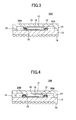
FIG. 3 is a cross-sectional view of a semiconductor device of a first embodiment of the present invention; -
FIG. 4 is a cross-sectional view of a semiconductor device of a first modified example of the first embodiment of the present invention; -
FIG. 5 is a cross-sectional view of a semiconductor device of a second modified example of the first embodiment of the present invention; -
FIG. 6 is a cross-sectional view of a semiconductor device of a second embodiment of the present invention; and -
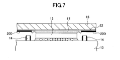
FIG. 7 is an expanded cross-sectional view showing the vicinity of a thermal connecting part ofFIG. 6 . -
- 10A through 10D
- semiconductor device
- 12
- semiconductor element
- 13
- package board
- 14
- chip component
- 15
- lid
- 17
- thermal connecting member
- 20A through 20D
- adhesion preventing sheet
- 22
- gold plating film
- A description is given below, with reference to the
FIG. 3 through FIG. 7 of embodiments of the present invention. -
FIG. 3 is a cross-sectional view of asemiconductor device 10A of a first embodiment of the present invention. Thesemiconductor device 10A includes asemiconductor element 12, apackage board 13,chip components 14, alid 15, a thermal connectingmember 17,adhesion preventing sheets 20A, and others. - The
semiconductor element 12 is a high density element and generates a great amount of heat. Thesemiconductor element 12 is flip chip mounted on thepackage board 13. More specifically, solder bumps 17 are provided on a main surface of thesemiconductor element 12. Thesemiconductor element 12 is mounted on thepackage board 13 by connecting the solder bumps 18 to bonding pads (not shown inFIG. 3 ) formed on a surface of thepackage board 13. In addition,underfill resin 19 is provided between thesemiconductor element 12 and thepackage board 13 so as to reinforce the solder bumps 18. - The
package board 13 is, for example, a multilayer printed wiring board. Thechip components 14, thelid 15 and theadhesion preventing sheets 20A, along with thesemiconductor element 12, are provided on the upper surface of thepackage board 13. In addition,solder balls 16 as external connection terminals are provided on the rear surface of thepackage board 13. Thesemiconductor element 12 and thesolder balls 16 are electrically connected to each other by interlayer wirings or the like provided in thepackage board 13. - The
chip component 14 is an electronic component such as a surface terminal type capacitor. Thechip components 14 are provided in external circumferential positions relative to thesemiconductor element 12. Thechip component 14 has the same structure as that of thechip component 4 shown inFIG. 2(A) . Solder arranging parts (not shown) connect thechip components 4 to thepackage board 13. - The
lid 15 is made of a metal material having high conductivity and works as a heat radiating member. Thelid 15 is fixed to thepackage board 13 by using, for example, an adhesive. Furthermore, thelid 15 has a cap-shaped configuration and covers the substantially entire upper surface of thepackage board 13. Accordingly, thesemiconductor element 12 and thechip components 14 are sealed inside thelid 15 by thelid 15 being fixed to thepackage board 13. - The thermal connecting
member 17 is provided between thesemiconductor element 12 and thelid 15. The thermal connectingmember 17 is configured to thermally connect thesemiconductor element 12 and thelid 15 to each other. The thermal connectingmember 17 is made of a metal material having high thermal conductivity. In this embodiment, solder is used as the metal material forming the thermal connectingmember 17. Since it is possible to thermally connect thesemiconductor element 12 and thelid 15 to each other by a soldering process using the solder that is the metal material forming the thermal connectingmember 17, it is possible to thermally connect thesemiconductor element 12 and thelid 15 with a simple process. - As discussed above, by thermally connecting the
semiconductor element 12 and thelid 15 with the thermal connectingmember 17 having high thermal conductivity, it is possible to efficiently transfer heat generated by thesemiconductor element 12 to thelid 15 and radiate the heat. However, in a case where solder is used as the thermal connectingmember 17, as discussed above, the thermal connecting member is melted along with thesolder balls 16 by heat applied for mounting so as to flow along the internal surface of thelid 15. As a result of this, a part of the thermal connectingmember 17 may flow down and be adhered to thechip components 14. - Because of this, in the
semiconductor device 10A, anadhesion preventing member 20A is provided so as to prevent the thermal connecting member (solder) 17, which is melted and flows at the heating time, being adhered to thechip components 14. In this example, theadhesion preventing sheets 20A are provided as an adhesion preventing part. Theadhesion preventing sheets 20A are made of resin such as polyimide and have upside-down bent L-shaped configurations. Furthermore, one end of theadhesion preventing sheet 20A is adhered and fixed to thepackage board 13 and another end of theadhesion preventing sheet 20A is a free end. In addition, theadhesion preventing sheets 20A are fixed to thepackage board 13 in a position closer to thesemiconductor element 12 than are thechip components 14. Theadhesion preventing sheets 20A are separated from thechip components 14 and cover at least the entire upper surfaces of thechip components 14. - Because of this, even if solder is used as the thermal connecting
member 17 or the thermal connectingmember 17 is made molten by heat for mounting or the like and flows down from thelid 15 to thechip components 14, the melted solder of the thermal connectingmember 17 is received by theadhesion preventing sheet 20A having the structures discussed above. Hence, it is possible to prevent the melted thermal connectingmember 17 from being adhered to thechip components 14. - In addition, the
adhesion preventing sheet 20A are provided so as to be separated from thechip components 14. Because of this, thechip components 4 discussed with reference toFIG. 2 are completely sealed by the sealingresin 9. Hence, even if the solder arranging parts of thechip components 14 are melted and expanded due to the heat, it is possible to prevent generation of electric shorts between the neighboring solder arranging parts. - According to the
semiconductor device 10A of this example, it is possible to effectively prevent electric shorts due to the melted thermal connectingmember 17 and electric short due to the solder arranging parts. Hence, it is possible to improve reliability of thesemiconductor device 10A. In addition, by using the sheet-shapedadhesion preventing sheet 20A as the adhesion preventing part, it is possible to prevent the melted thermal connectingmember 17 from being adhered to thechip components 14 with a simple structure. - Furthermore, since the sheet-shaped
adhesion preventing sheet 20A is thin, providing theadhesion preventing sheet 20A does not cause thesemiconductor device 10A to have a large size (high tall). In addition, since only one end of each of the adhesion preventing sheets is fixed to thepackage board 13, it is possible to reduce the amount of the adhesive used. -
FIG. 4 shows a first modified example of thesemiconductor device 10A of the first embodiment of the present invention.FIG. 5 shows a second modified example of thesemiconductor device 10A of the first embodiment of the present invention. InFIG. 4 andFIG. 5 , parts that are the same as the parts shown inFIG. 3 are given the same reference numerals, and explanation thereof is omitted. In addition, inFIG. 6 andFIG. 7 referring to the explanation of a second embodiment of the present invention, parts that are the same as the parts shown inFIG. 3 are given the same reference numerals, and explanation thereof is omitted. - In the
semiconductor device 10A of the first embodiment of the present invention discussed above, only one end of each of theadhesion preventing sheets 20A is fixed to thepackage board 13. On the other hand, in asemiconductor device 10B of the first modified example shown inFIG. 4 , both ends ofadhesion preventing sheets 20B are fixed to thepackage board 13. Because of this structure, it is possible to fix theadhesion preventing sheet 20B to thepackage board 13 more rigidly than the structure of the first embodiment. Accordingly, even if a large amount of the molten thermal connectingmember 17 flow down, it is possible to prevent generation of electric shorts. - In a semiconductor device 10C of the second modified example shown in
FIG. 5 ,adhesion preventing sheet 20C are supported bypillars 21 standing on thepackage board 13. In addition, openings are formed in portions corresponding to the position of thesemiconductor element 12. With this structure, theadhesion preventing sheet 20C covers a wider area of thepackage board 13 compared to thesemiconductor devices members 17 being adhered to otherelectronic components 23 provided on thepackage board 13 with thechip components 14, by a singleadhesion preventing sheet 20C. - Next, a semiconductor device 10C of the second embodiment of the present invention is discussed.
-
FIG. 6 is a cross-sectional view of a semiconductor device 10C of the second embodiment of the present invention.FIG. 7 is an expanded cross-sectional view showing the vicinity of a thermal connectingpart 17 ofFIG. 6 . In this embodiment, anadhesion preventing sheet 20D is provided at thelid 15 as the adhesion preventing part. - The
adhesion preventing sheet 20D is formed of sheet-shaped polyimide in this embodiment as well as the first embodiment. In addition, theadhesion preventing sheet 20D is adhered and fixed to the internal surface of thelid 15. Thus, by providing theadhesion preventing sheet 20D on the internal surface of thelid 15, theadhesion preventing sheet 20D is separated from thechip components 14. Furthermore, theadhesion preventing sheet 20D is positioned external to circumferential positions of an area where thelid 15 is thermally connected to the thermal connectingmember 17 and an area including a position facing at least thechip components 14. - As discussed above, the thermal connecting
member 17 may be melted by heat for mounting. In addition, the thermal connectingmember 17 is adhered to the internal surface of thelid 15 by soldering. Accordingly, a gold plating 22 (seeFIG. 7 ) is formed on the internal surface of thelid 15. Thegold plating 22 is configured to improve the ability to connect (wetability) to the thermal connectingmember 17 made of solder. In a case where the thermal connectingmember 17 can be well formed to thelid 15 by providing the gold plating 22 but the thermal connectingmember 17 is melted by heat for mounting, the thermal connectingmember 17 easily flow on the internal surface of thelid 15 due to thegold plating 22 having high wetability. - However, in the semiconductor device 10C of the second embodiment, the
adhesion preventing sheet 20D is provided on the internal surface of thelid 15, namely thegold plating 22. Therefore, flow of the melted thermal connectingmember 17 on the internal surface of thelid 15 is blocked by theadhesion preventing sheet 20D. In other words, theadhesion preventing sheet 20D works as a dam member configured to block the flow of the molten thermal connectingmember 17.FIG. 7 shows the flow of the melted thermal connectingmember 17 being blocked by theadhesion preventing sheet 20D. - Thus, in this embodiment as well as the first embodiment, it is possible to prevent the melted thermal connecting
member 17 from flowing down on thechip components 14. In addition, since theadhesion preventing sheet 20D is provided in a wide area even at upper parts of thechip components 14, even if a large amount of the thermal connectingmember 17 is melted and a part of the thermal connectingmember 17 goes to the upper part of theadhesion preventing sheet 20D, it is possible to prevent the part of the thermal connectingmembers 17 from flowing to the upper parts of thechip components 14. - Although the
adhesion preventing sheet 20D as the adhesion preventing part is fixed to thelid 15 in the second embodiment of the present invention, the present invention is not limited this. For example, a solder resist may be applied to thelid 15 and the same effect can be achieved in this case. - Although the invention has been described with respect to specific embodiment for a complete and clear disclosure, the appended claims are not to be thus limited but are to be construed as embodying all modifications and alternative constructions that may occur to one skilled in the art that fairly fall within the basic teachings herein set forth.
Claims (9)
- A semiconductor device, comprising:a board;a semiconductor element mounted on the board;an electronic component, with the semiconductor element, mounted on the board;a heat radiation member provided so as to face the board, the heat radiation member configured to radiate heat of the semiconductor element; anda thermal connecting member being configured to thermally connect the heat radiation member and the semiconductor element,wherein a metal material is used as the thermal connecting member, andan adhesion preventing member is provided so as to be separated from the electronic component, the adhesion preventing member being configured to prevent the metal material molten and flowing at a heating time being adhered to the electronic component.
- The semiconductor device as claimed in claim 1,
wherein solder is used as the metal material. - The semiconductor device as claimed in claim 1,
wherein the adhesion preventing member is a sheet-shaped covering member configured to cover the electronic component. - The semiconductor device as claimed in claim 1,
wherein the adhesion preventing member is a sheet-shaped covering member configured to cover the electronic component, and
one end of the covering member is fixed to the board and another end of the covering member is a free end. - The semiconductor device as claimed in claim 1,
wherein the adhesion preventing member is a sheet-shaped covering member configured to cover the electronic component, and
both ends of the covering member are fixed to the board. - The semiconductor device as claimed in claim 1,
wherein the adhesion preventing member is a sheet-shaped covering member configured to cover the electronic component, and
the covering member is made of polyimide. - The semiconductor device as claimed in claim 1,
wherein the adhesion preventing member is provided at an external circumferential position relative to a position where the thermal connecting member of the heat radiation member is thermally connected and a position facing at least the electronic component, and
the adhesion preventing member is configured to block the flow of the thermal connecting member on the heat radiation member at the time when the thermal connecting member is molten. - The semiconductor device as claimed in claim 1,
wherein the adhesion preventing member is provided at an external circumferential position relative to a position where the thermal connecting member of the heat radiation member is thermally connected and a position facing at least the electronic component, and
the adhesion preventing member includes a resin sheet. - The semiconductor device as claimed in claim 1,
wherein the adhesion preventing member is provided at an external circumferential position relative to a position where the thermal connecting member of the heat radiation member is thermally connected and a position facing at least the electronic component, and
gold plating is applied on a surface of the heat radiation member thermally connected to the thermal connecting member.
Applications Claiming Priority (1)
| Application Number | Priority Date | Filing Date | Title |
|---|---|---|---|
| PCT/JP2006/303386 WO2007096975A1 (en) | 2006-02-24 | 2006-02-24 | Semiconductor device |
Publications (2)
| Publication Number | Publication Date |
|---|---|
| EP1988574A1 true EP1988574A1 (en) | 2008-11-05 |
| EP1988574A4 EP1988574A4 (en) | 2011-10-05 |
Family
ID=38437037
Family Applications (1)
| Application Number | Title | Priority Date | Filing Date |
|---|---|---|---|
| EP06714525A Withdrawn EP1988574A4 (en) | 2006-02-24 | 2006-02-24 | SEMICONDUCTOR DEVICE |
Country Status (6)
| Country | Link |
|---|---|
| US (1) | US7834443B2 (en) |
| EP (1) | EP1988574A4 (en) |
| JP (1) | JP4874325B2 (en) |
| KR (1) | KR101007958B1 (en) |
| CN (1) | CN101379612B (en) |
| WO (1) | WO2007096975A1 (en) |
Cited By (1)
| Publication number | Priority date | Publication date | Assignee | Title |
|---|---|---|---|---|
| EP3923317A4 (en) * | 2019-02-04 | 2022-11-30 | Sony Interactive Entertainment Inc. | ELECTRONIC APPARATUS, SEMICONDUCTOR DEVICE, INSULATION SHEET, AND SEMICONDUCTOR DEVICE MANUFACTURING METHOD |
Families Citing this family (11)
| Publication number | Priority date | Publication date | Assignee | Title |
|---|---|---|---|---|
| JP5153316B2 (en) * | 2007-12-21 | 2013-02-27 | 新光電気工業株式会社 | Semiconductor package heat sink and plating method thereof |
| CA2783542C (en) * | 2009-12-14 | 2015-10-13 | Hdt Robotics, Inc. | One motor finger mechanism |
| JP5573645B2 (en) * | 2010-12-15 | 2014-08-20 | 富士通セミコンダクター株式会社 | Semiconductor device and manufacturing method of semiconductor device |
| JP2013115083A (en) * | 2011-11-25 | 2013-06-10 | Fujitsu Semiconductor Ltd | Semiconductor device and method of manufacturing the same |
| JP5861580B2 (en) * | 2012-07-09 | 2016-02-16 | 株式会社ソシオネクスト | Semiconductor device and semiconductor device manufacturing method |
| CN103117275B (en) * | 2013-01-31 | 2015-08-19 | 华为技术有限公司 | A kind of chip-packaging structure and chip packaging method |
| CN109755197A (en) * | 2019-01-14 | 2019-05-14 | 苏州通富超威半导体有限公司 | Encapsulating structure and forming method thereof |
| JP7342367B2 (en) * | 2019-01-28 | 2023-09-12 | 株式会社デンソー | electronic control unit |
| CN110416097B (en) * | 2019-06-12 | 2021-05-11 | 苏州通富超威半导体有限公司 | Packaging structure and packaging method for preventing indium metal from overflowing |
| JP7242824B1 (en) | 2021-12-16 | 2023-03-20 | レノボ・シンガポール・プライベート・リミテッド | Heat dissipation structure and electronic equipment |
| CN115939053A (en) * | 2022-05-20 | 2023-04-07 | 江苏芯德半导体科技有限公司 | A semiconductor packaging structure |
Family Cites Families (10)
| Publication number | Priority date | Publication date | Assignee | Title |
|---|---|---|---|---|
| JPS60242647A (en) | 1984-05-16 | 1985-12-02 | Mitsubishi Electric Corp | Mounting method of hybrid integrated circuit |
| JP2538922B2 (en) * | 1987-06-12 | 1996-10-02 | 株式会社日立製作所 | Semiconductor device |
| JPH0279451A (en) * | 1988-09-14 | 1990-03-20 | Hitachi Ltd | Semiconductor device, its cooling and manufacturing methods |
| US6313521B1 (en) * | 1998-11-04 | 2001-11-06 | Nec Corporation | Semiconductor device and method of manufacturing the same |
| JP2001267473A (en) * | 2000-03-17 | 2001-09-28 | Hitachi Ltd | Semiconductor device and method of manufacturing the same |
| JP2001308215A (en) * | 2000-04-24 | 2001-11-02 | Ngk Spark Plug Co Ltd | Semiconductor device |
| US6773963B2 (en) | 2002-01-16 | 2004-08-10 | Intel Corporation | Apparatus and method for containing excess thermal interface material |
| JP2004071977A (en) * | 2002-08-08 | 2004-03-04 | Mitsubishi Electric Corp | Semiconductor device |
| US6992891B2 (en) | 2003-04-02 | 2006-01-31 | Intel Corporation | Metal ball attachment of heat dissipation devices |
| JP2005228811A (en) * | 2004-02-10 | 2005-08-25 | Renesas Technology Corp | Semiconductor device |
-
2006
- 2006-02-24 EP EP06714525A patent/EP1988574A4/en not_active Withdrawn
- 2006-02-24 JP JP2008501532A patent/JP4874325B2/en not_active Expired - Fee Related
- 2006-02-24 CN CN200680053103.8A patent/CN101379612B/en not_active Expired - Fee Related
- 2006-02-24 KR KR1020087020241A patent/KR101007958B1/en not_active Expired - Fee Related
- 2006-02-24 WO PCT/JP2006/303386 patent/WO2007096975A1/en not_active Ceased
-
2008
- 2008-08-05 US US12/222,233 patent/US7834443B2/en not_active Expired - Fee Related
Cited By (1)
| Publication number | Priority date | Publication date | Assignee | Title |
|---|---|---|---|---|
| EP3923317A4 (en) * | 2019-02-04 | 2022-11-30 | Sony Interactive Entertainment Inc. | ELECTRONIC APPARATUS, SEMICONDUCTOR DEVICE, INSULATION SHEET, AND SEMICONDUCTOR DEVICE MANUFACTURING METHOD |
Also Published As
| Publication number | Publication date |
|---|---|
| KR101007958B1 (en) | 2011-01-14 |
| JPWO2007096975A1 (en) | 2009-07-09 |
| CN101379612B (en) | 2014-07-09 |
| WO2007096975A1 (en) | 2007-08-30 |
| US7834443B2 (en) | 2010-11-16 |
| EP1988574A4 (en) | 2011-10-05 |
| CN101379612A (en) | 2009-03-04 |
| KR20080092967A (en) | 2008-10-16 |
| JP4874325B2 (en) | 2012-02-15 |
| US20080296755A1 (en) | 2008-12-04 |
Similar Documents
| Publication | Publication Date | Title |
|---|---|---|
| US7834443B2 (en) | Semiconductor device with molten metal preventing member | |
| EP0594395B1 (en) | Semiconductor power module | |
| US6317326B1 (en) | Integrated circuit device package and heat dissipation device | |
| US6424033B1 (en) | Chip package with grease heat sink and method of making | |
| US9806051B2 (en) | Ultra-thin embedded semiconductor device package and method of manufacturing thereof | |
| US7679182B2 (en) | Power module and motor integrated control unit | |
| CN1319422C (en) | Hybrid module and making method thereof and mounting method thereof | |
| JP3644662B2 (en) | Semiconductor module | |
| US8089146B2 (en) | Semiconductor device and heat radiation member | |
| US20040080036A1 (en) | System in package structure | |
| US6335563B1 (en) | Semiconductor device, method of fabricating the same, circuit board, and electronic device | |
| KR101343199B1 (en) | Semiconductor device package | |
| JP4056598B2 (en) | Infrared data communication module | |
| US20080036049A1 (en) | Stacked integration module and method for manufacturing the same | |
| EP3588557B1 (en) | Package structure | |
| US7310224B2 (en) | Electronic apparatus with thermal module | |
| US7190063B2 (en) | Semiconductor device and method of manufacturing the same, circuit board, and electronic apparatus | |
| US8569881B2 (en) | Semiconductor device | |
| US20050212148A1 (en) | Semiconductor device | |
| JP2746248B2 (en) | Chip carrier and method of soldering chip carrier | |
| KR100230919B1 (en) | Semiconductor package | |
| JP2007157801A (en) | Semiconductor module and manufacturing method thereof | |
| JPH11111882A (en) | Wiring board for BGA type semiconductor device and BGA type semiconductor device | |
| JPH08255853A (en) | Electronic component mounting device | |
| JP3314139B2 (en) | Semiconductor device |
Legal Events
| Date | Code | Title | Description |
|---|---|---|---|
| PUAI | Public reference made under article 153(3) epc to a published international application that has entered the european phase |
Free format text: ORIGINAL CODE: 0009012 |
|
| 17P | Request for examination filed |
Effective date: 20080901 |
|
| AK | Designated contracting states |
Kind code of ref document: A1 Designated state(s): DE FR GB |
|
| DAX | Request for extension of the european patent (deleted) | ||
| RBV | Designated contracting states (corrected) |
Designated state(s): DE FR GB |
|
| A4 | Supplementary search report drawn up and despatched |
Effective date: 20110901 |
|
| RIC1 | Information provided on ipc code assigned before grant |
Ipc: H01L 23/42 20060101ALI20110826BHEP Ipc: H01L 25/00 20060101AFI20110826BHEP Ipc: H01L 23/36 20060101ALI20110826BHEP Ipc: H01L 23/12 20060101ALI20110826BHEP Ipc: H01L 25/16 20060101ALI20110826BHEP Ipc: H01L 21/48 20060101ALI20110826BHEP Ipc: H01L 23/64 20060101ALI20110826BHEP |
|
| 17Q | First examination report despatched |
Effective date: 20150203 |
|
| STAA | Information on the status of an ep patent application or granted ep patent |
Free format text: STATUS: THE APPLICATION IS DEEMED TO BE WITHDRAWN |
|
| 18D | Application deemed to be withdrawn |
Effective date: 20150616 |