EP1983647A2 - Surface acoustic wave device and duplexer - Google Patents
Surface acoustic wave device and duplexer Download PDFInfo
- Publication number
- EP1983647A2 EP1983647A2 EP08103546A EP08103546A EP1983647A2 EP 1983647 A2 EP1983647 A2 EP 1983647A2 EP 08103546 A EP08103546 A EP 08103546A EP 08103546 A EP08103546 A EP 08103546A EP 1983647 A2 EP1983647 A2 EP 1983647A2
- Authority
- EP
- European Patent Office
- Prior art keywords
- substrate
- acoustic wave
- axis
- surface acoustic
- wave device
- Prior art date
- Legal status (The legal status is an assumption and is not a legal conclusion. Google has not performed a legal analysis and makes no representation as to the accuracy of the status listed.)
- Granted
Links
- 238000010897 surface acoustic wave method Methods 0.000 title claims abstract description 34
- 239000000758 substrate Substances 0.000 claims abstract description 95
- 229910012463 LiTaO3 Inorganic materials 0.000 claims abstract description 10
- 229910052594 sapphire Inorganic materials 0.000 claims description 22
- 239000010980 sapphire Substances 0.000 claims description 22
- 230000000052 comparative effect Effects 0.000 description 16
- 230000000644 propagated effect Effects 0.000 description 5
- 230000008878 coupling Effects 0.000 description 3
- 238000010168 coupling process Methods 0.000 description 3
- 238000005859 coupling reaction Methods 0.000 description 3
- 238000006073 displacement reaction Methods 0.000 description 3
- 239000000463 material Substances 0.000 description 3
- 230000001902 propagating effect Effects 0.000 description 3
- 230000005540 biological transmission Effects 0.000 description 2
- 230000001413 cellular effect Effects 0.000 description 2
- WSMQKESQZFQMFW-UHFFFAOYSA-N 5-methyl-pyrazole-3-carboxylic acid Chemical compound CC1=CC(C(O)=O)=NN1 WSMQKESQZFQMFW-UHFFFAOYSA-N 0.000 description 1
- 229910003327 LiNbO3 Inorganic materials 0.000 description 1
- XAGFODPZIPBFFR-UHFFFAOYSA-N aluminium Chemical compound [Al] XAGFODPZIPBFFR-UHFFFAOYSA-N 0.000 description 1
- 229910052782 aluminium Inorganic materials 0.000 description 1
- 239000013078 crystal Substances 0.000 description 1
- 238000010586 diagram Methods 0.000 description 1
- 239000011521 glass Substances 0.000 description 1
- GQYHUHYESMUTHG-UHFFFAOYSA-N lithium niobate Chemical compound [Li+].[O-][Nb](=O)=O GQYHUHYESMUTHG-UHFFFAOYSA-N 0.000 description 1
- 238000000034 method Methods 0.000 description 1
- 238000010295 mobile communication Methods 0.000 description 1
- 230000000452 restraining effect Effects 0.000 description 1
- 229910052710 silicon Inorganic materials 0.000 description 1
- 239000010703 silicon Substances 0.000 description 1
- 238000004088 simulation Methods 0.000 description 1
Images





Classifications
-
- H—ELECTRICITY
- H03—ELECTRONIC CIRCUITRY
- H03H—IMPEDANCE NETWORKS, e.g. RESONANT CIRCUITS; RESONATORS
- H03H9/00—Networks comprising electromechanical or electro-acoustic elements; Electromechanical resonators
- H03H9/02—Details
- H03H9/02535—Details of surface acoustic wave devices
- H03H9/02543—Characteristics of substrate, e.g. cutting angles
- H03H9/02559—Characteristics of substrate, e.g. cutting angles of lithium niobate or lithium-tantalate substrates
-
- H—ELECTRICITY
- H03—ELECTRONIC CIRCUITRY
- H03H—IMPEDANCE NETWORKS, e.g. RESONANT CIRCUITS; RESONATORS
- H03H9/00—Networks comprising electromechanical or electro-acoustic elements; Electromechanical resonators
- H03H9/46—Filters
- H03H9/64—Filters using surface acoustic waves
-
- H—ELECTRICITY
- H03—ELECTRONIC CIRCUITRY
- H03H—IMPEDANCE NETWORKS, e.g. RESONANT CIRCUITS; RESONATORS
- H03H9/00—Networks comprising electromechanical or electro-acoustic elements; Electromechanical resonators
- H03H9/02—Details
- H03H9/02535—Details of surface acoustic wave devices
- H03H9/02543—Characteristics of substrate, e.g. cutting angles
- H03H9/02574—Characteristics of substrate, e.g. cutting angles of combined substrates, multilayered substrates, piezoelectrical layers on not-piezoelectrical substrate
-
- H—ELECTRICITY
- H03—ELECTRONIC CIRCUITRY
- H03H—IMPEDANCE NETWORKS, e.g. RESONANT CIRCUITS; RESONATORS
- H03H9/00—Networks comprising electromechanical or electro-acoustic elements; Electromechanical resonators
- H03H9/70—Multiple-port networks for connecting several sources or loads, working on different frequencies or frequency bands, to a common load or source
- H03H9/72—Networks using surface acoustic waves
-
- H—ELECTRICITY
- H03—ELECTRONIC CIRCUITRY
- H03H—IMPEDANCE NETWORKS, e.g. RESONANT CIRCUITS; RESONATORS
- H03H9/00—Networks comprising electromechanical or electro-acoustic elements; Electromechanical resonators
- H03H9/02—Details
- H03H9/02535—Details of surface acoustic wave devices
- H03H9/02818—Means for compensation or elimination of undesirable effects
- H03H9/02866—Means for compensation or elimination of undesirable effects of bulk wave excitation and reflections
-
- H—ELECTRICITY
- H03—ELECTRONIC CIRCUITRY
- H03H—IMPEDANCE NETWORKS, e.g. RESONANT CIRCUITS; RESONATORS
- H03H9/00—Networks comprising electromechanical or electro-acoustic elements; Electromechanical resonators
- H03H9/46—Filters
- H03H9/64—Filters using surface acoustic waves
- H03H9/6423—Means for obtaining a particular transfer characteristic
- H03H9/6433—Coupled resonator filters
- H03H9/6483—Ladder SAW filters
Definitions
- the present invention generally relates to a surface acoustic wave device and a duplexer, and more particularly, to a surface acoustic wave device and a duplexer in which a piezoelectric substrate is joined on a supporting substrate.
- a high-frequency band such as a frequency band from 800 MHz to 1.0 GHz and from 1.5 GHz to 2.0 GHz is used for cellular phones.
- a surface acoustic wave device such as a surface acoustic wave filter and a duplexer are used in this area,
- a piezoelectric substrate used for surface acoustic wave devices such as a LiTaO 3 (lithium tantalate) LiNbO 3 (lithium niobate) substrate has an advantage that a large electromechanical coupling coefficient is available, and a disadvantage that the resonance (or anti-resonance) frequency thereof depends on temperature greatly.
- crystal has a resonance (or anti-resonance) frequency that does not depend on temperature greatly, while having a small electromechanical coupling coefficient.
- Documents 1,2 and 3 disclose a surface acoustic wave device in which a LiTaO 3 piezoelectric substrate is joined on a sapphire substrate and an electrode pattern such as IDT (InterDigital Transducer) is provided on the piezoelectric substrate.
- IDT InterDigital Transducer
- the LiTaO 3 piezoelectric substrate (an LT substrate) has a normal line direction on the surface thereof in a direction that is rotated 42° from a Y axis to a Z axis direction about an X axis in which a surface acoustic wave is propagated (this is called a 42° cut substrate).
- the 42° cut substrate is mainly used for the surface acoustic wave device including the LT substrate, since the propagation loss thereof is small.
- ripples are generated in a resonance characteristic of resonator or a pass band of filter.
- the present invention has been made in view of the above-mentioned circumstances and provides a surface acoustic wave device joining a LiTaO 3 piezoelectric substrate on a supporting substrate, in which a ripple is restrained.
- a surface acoustic wave device including: a supporting substrate; a LiTaO3 piezoelectric substrate joined on the supporting substrate, which has a normal line direction on a main surface thereof in a direction rotated 43° to 53° from a Y axis to a Z axis direction about an X axis; and an electrode pattern formed on the piezoelectric substrate.
- a duplexer including: a common terminal; and a first filter and a second filter connected to the common terminal, wherein at least one of the first and second filters is configured as mentioned above.
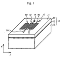
- Fig. 1 is a perspective view of a surface acoustic wave resonator formed by joining a LiTaO3 piezoelectric substrate (hereinafter an LT substrate) 20 on a sapphire substrate 10 (a supporting substrate).
- the LT substrate 20 having a film thickness of 40 ⁇ m is joined on the sapphire substrate 10 having a film thickness of 250 ⁇ m so as to form an LT/sapphire substrate 15.
- the same method of forming the LT/sapphire substrate 15 as described in Documents 2 and 3 is employed to the present embodiment.
- an amorphous joining region 12 having a thickness of 0.3 ⁇ 2.5 nm is provided at a joined interface between the sapphire substrate 10 and the LT substrate 20.
- the interface between the sapphire substrate 10 and the LT substrate 20 is substantially smooth, although having a slight roughness caused by forming the amorphous joining region 12.
- An electrode IDT and reflectors RO as an electrode pattern 22 made ofAl (aluminum) are provided on the LT substrate 20.
- a propagating direction of the surface acoustic wave is in the X axis, and the reflectors RO are respectively provided on both sides of the IDT in the direction of the X axis.
- the IDT has an input terminal In and an output terminal Out so as to function as a resonator 25.
- the wavelength of the surface acoustic wave is approximately 4 ⁇ m.
- the normal line direction of a main surface 21 of the LT substrate 20 is an N direction.
- the N direction is the direction that is rotated 42° from the Y axis to the Z axis about the X axis, which is the propagating direction of the surface acoustic wave.
- the 42' Y cut LT/sapphire substrate is used in the present surface acoustic wave device.
- Fig. 2A is a graph of a band-pass characteristic in which the resonator 25 using the 42° Y cut LT/sapphire substrate of a first comparative example is used as a series resonator
- Fig. 2B is an enlarged graph of an area including the resonance point.
- a ripple is observed at a frequency of about 935 MHz, which is a little higher than an anti-resonance point.
- Fig. 2B another ripple is observed at a frequency of about 905 MHz, which is a little lower than the resonance point.
- Fig. 3A is a graph of a band-pass characteristic in which the resonator 25 using the 42° Y cut LT/sapphire substrate of the first comparative example is a parallel resonator
- Fig. 3B is an enlarged graph of an area including the anti-resonance point. Referring to Fig. 3B , ripples are observed at a frequency of about 880 MHz, which is a little lower than the anti-resonance point, and at frequency of about 910MHz, which is a little higher than the anti-resonance frequency.
- Fig. 4 is a cross-sectional view of the resonator 25 shown in Fig. 1 .
- the joint interface In order to secure a joining strength of the LT substrate 20 and the sapphire substrate 10, the joint interface should be substantially smooth. If the joint interface has a roughness, the coupling strength is degraded. If the joint interface is smooth, however, the bulk waves reflected at the interface between the LT substrate 20 and the sapphire substrate 10 are propagated as shown in Fig. 4 since the LT substrate 20 is as thin as 10 ⁇ ( ⁇ is the wavelength of the surface acoustic wave). The unwanted responses caused by the bulk waves are observed as ripples in Figs. 2A through 3B .
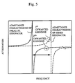
- Fig. 5 schematically shows admittance characteristics of the series and parallel resonators that compose a ladder filter, according to the band-pass characteristics of the resonator 25 of the first comparative example shown in Figs. 2A through 3B .
- a first unwanted response and a second unwanted response are generated in a pass-band of the filter. If the interface between the LT substrate 20 and the sapphire substrate 10 is uneven, the bulk waves reflected at the interface are scattered. It is thus possible to restrain the unwanted responses in Fig. 5 . On the contrary, it is preferable that the interface has a smoothness in order to restrain bulk waves reflected by the interface from being scattered and to secure the joining strength of the LT substrate 20 and the sapphire substrate 10.
- an LT cut angle is changed to simulate the magnitude of the second unwanted response in Fig. 5 , in order to solve the above-mentioned problem.
- the LT cut angle is the angle in which the normal line direction of the main surface of the LT substrate 20 is rotated from the Y axis to the Z axis about the X axis, which is the propagating direction of the surface acoustic wave.
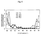
- Fig. 6 is a graph showing unwanted responses observed at LT cut angles of 38° ⁇ 54° and normalized by the unwanted response observed at the 42° LT cut angle.
- the simulation set the thickness of the LT substrate equal to 7 ⁇ , 10 ⁇ , 15 ⁇ and 20 ⁇ ( ⁇ is the wavelength of the surface acoustic wave).
- the electrode pattern 22 was made of Al and had a film thickness of 0.1 ⁇ .
- the normalized unwanted response is less than or equal to 1 for each film thickness of the LT substrate 20. That is, the unwanted response can be reduced, as compared to the general cases using an LT cut angle of 42.
- the normalized unwanted response is less than or equal to 1 when the film thickness of the LT substrate 20 is 7 ⁇ of 10 ⁇ .
- the normalized unwanted response is less than or equal to 0.2 and is substantially constant.
- the LT cut angle should be 43° ⁇ 53°, preferably should be 43° ⁇ 52°, more preferably should be 46° ⁇ 50°.
- the film thickness of the electrode pattern 22 influences the band-pass characteristic of the resonator using the surface acoustic wave.
- the unwanted response caused by the bulk wave shown in Fig. 4 is not influenced by the film thickness of the electrode pattern 22.
- the electrode pattern 22 is provided on the surface of the LT substrate 20, the impedance of the resonator is remarkably small.
- the impedance of the resonator is remarkably large. In the boundary of the electrode pattern 22 having great impedance difference on the surface of the LT substrate 20, the bulk wave is emitted in the LT substrate 20.
- the bulk wave is then reflected on the boundary between the LT substrate 20 and the sapphire substrate 10.
- the reflected bulk wave is absorbed into the electrode pattern 22 on the surface of LT substrate 20, and becomes an unwanted response.
- the bulk wave is merely propagated in the LT substrate 20, the film thickness of the electrode pattern 22 hardly influences the magnitude of unwanted response.
- Fig. 6 shows that the magnitude of unwanted response depends on the film thickness of the LT substrate 20.
- the film thickness of the LT substrate 20 hardly influences the dependence of unwanted response on the LT cut angle.
- the preferable range of the LT cut angle hardly depends on the film thickness of the LT substrate 20.
- Fig. 7 is a graph that shows a displacement distribution of a Leaky surface acoustic wave propagated on the surface of the LT substrate 20 in the depth direction.
- the displacement of the Leaky surface acoustic wave is almost at depths equal to or less than 1 ⁇ ( ⁇ is the wavelength of the surface acoustic wave). Therefore, the film thickness of the LT substrate 20 is preferably more than or equal to 1 ⁇ . Further, it is preferable that the LT substrate 20 has a thickness of less than or equal to 100 ⁇ , since it is rather meaningless to provide the supporting substrate when the LT substrate 20 has a thickness more than 100 ⁇ .
- a second embodiment is a ladder filter having a pass band at a frequency of 900 MHz.
- a ladder filter 28 is composed of series resonators S I through S3 and parallel resonators P1 and P2.
- the series resonators S1 through S3 are connected in series between an input terminal In and an output terminal Out.
- the parallel resonator P1 is connected between a node and ground, the node being between the series resonators S1 and S2.
- the parallel resonator P2 is connected between another node and the ground, the another node being between the series resonators S2 and S3.
- Fig. 9A is a graph of band-pass characteristics of two ladder filters that have a pass band ranging from 880 MHz to 915 MHz and include the respective LT/sapphire substrates 15 having LT cut angles of 42° (a second comparative example) and 48° (the second embodiment).
- Fig. 9B is an enlarged graph of the pass bands of the two ladder filters. Referring to Fig. 9B , the second comparative example has a first ripple and a second ripple respectively observed at frequencies of 883 MHz and 915 MHz. The second ripple is remarkably large, and the shoulder on the high frequency side of the pass band comes down.
- the first ripple is influenced by ripples generated on the parallel resonators and the second ripple is influenced by ripples generated on the series and parallel resonators.
- the first and second ripples are not observed in the second embodiment.
- the unique LT cunt angle restrains ripples occurred in the pass band of the ladder filter 28.
- a third embodiment is a ladder filter having a pass band at a frequency of 1900 MHz.
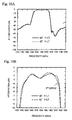
- Fig. 10A is a graph of band-pass characteristics of two ladder filters that have a pass band at a frequency of around 1900 MHz and include the respective LT/sapphire substrates 15 having LT cut angles of 42' (a third comparative example) and 46' (the third embodiment).
- Fig. 10B is an enlarged graph of the pass bands of the two ladder filters. Referring to Fig. 10B , a third ripple is observed at a frequency of 1915 MHz in the third comparative example. The ripple resulting from the parallel resonator is generated outside of the pass band in the third comparative example. Thus, the third ripple resulting from the series resonator is observed in the pass band, In contrast, the third ripple is restrained in the third embodiment.
- the present invention is not limited to the ladder filters in the second and third embodiments, but includes another type of filter such as a multiple mode filter in which the ripples caused by the unwanted responses of the bulk wave can be restrained.
- a fourth embodiment shown in Fig. 11 is an exemplary duplexer using at least one ladder filter 28 of the second or third embodiment.
- a first filter 30 as a transmission filter is connected between a common terminal Ant and a first terminal T1
- a second filter 40 as a reception filter is connected between the common terminal Ant and a second terminal T2.
- At least one of the first and second filters 30 and 40 can be the ladder filter 28 of the second or third embodiment.
- the ripples can be restrained in the pass band of the duplexer 50.
- the first and second filters 30 and 40 are not limited to the ladder filters but may be multiple mode filters.
- the first filter 30 on the transmission side may be a ladder filter and the second filter 40 on the reception side may be a DMS (double mode SAW) filter.
- the first and second filters 30 and 40 are made of respective substrates having different LT cut angles.
- the supporting substrate that supports the piezoelectric substrate is not limited to the sapphire substrate 10 used in the first through fourth embodiments.
- the supporting substrate may be made of a material that restrains the frequency-temperature characteristic, that is, a material having a smaller linear expansion coefficient than that of LiTaO 3 .
- glass or silicon may be used.
- the bulk wave shown in Fig. 4 behaves similarly in any material of the supporting substrate, thus the result shown in Fig. 6 can be applied to other supporting substrates. It is preferable, however, to use sapphire as the supporting substrate, since sapphire has a large Young's modulus.
Landscapes
- Physics & Mathematics (AREA)
- Acoustics & Sound (AREA)
- Chemical & Material Sciences (AREA)
- Engineering & Computer Science (AREA)
- Materials Engineering (AREA)
- Surface Acoustic Wave Elements And Circuit Networks Thereof (AREA)
Abstract
Description
- The present invention generally relates to a surface acoustic wave device and a duplexer, and more particularly, to a surface acoustic wave device and a duplexer in which a piezoelectric substrate is joined on a supporting substrate.
- Recently, cellular phones, personal digital accesses and the like have been spread rapidly according to the progress of the mobile communication system. For example, a high-frequency band such as a frequency band from 800 MHz to 1.0 GHz and from 1.5 GHz to 2.0 GHz is used for cellular phones. A surface acoustic wave device such as a surface acoustic wave filter and a duplexer are used in this area,
- A piezoelectric substrate used for surface acoustic wave devices such as a LiTaO3 (lithium tantalate) LiNbO3 (lithium niobate) substrate has an advantage that a large electromechanical coupling coefficient is available, and a disadvantage that the resonance (or anti-resonance) frequency thereof depends on temperature greatly. In contrast, crystal has a resonance (or anti-resonance) frequency that does not depend on temperature greatly, while having a small electromechanical coupling coefficient.
- Japanese Patent Application Publication Nos.
2004-186868 2005-252550 2004-343359 Documents - In
Documents Documents 1 through 3, ripples are generated in a resonance characteristic of resonator or a pass band of filter. - The present invention has been made in view of the above-mentioned circumstances and provides a surface acoustic wave device joining a LiTaO3 piezoelectric substrate on a supporting substrate, in which a ripple is restrained.
- According to an aspect of the present invention, there is provided a surface acoustic wave device including: a supporting substrate; a LiTaO3 piezoelectric substrate joined on the supporting substrate, which has a normal line direction on a main surface thereof in a direction rotated 43° to 53° from a Y axis to a Z axis direction about an X axis; and an electrode pattern formed on the piezoelectric substrate.
- According to another aspect of the present invention, there is provided a duplexer including: a common terminal; and a first filter and a second filter connected to the common terminal, wherein at least one of the first and second filters is configured as mentioned above.
-
-
Fig. 1 is a perspective view of a resonator in accordance with a first comparative example and a first embodiment; -
Figs. 2A and 2B are graphs of a band-pass characteristic when the resonator in accordance with the first comparative example is a series resonator; -
Figs. 3A and 3B are graphs of a band-pass characteristic when the resonator in accordance with the first comparative example is a parallel resonator; -
Fig. 4 schematically shows a bulk wave that causes an unwanted response in the first comparative example; -
Fig. 5 schematically shows admittance characteristics of the series and parallel resonators in the first comparative example; -
Fig. 6 is a graph of a normalized unwanted response as a function of an, LT cut angle; -
Fig. 7 is a graph of a depth as a function of a normalized displacement; -
Fig. 8 is a perspective view of a filter in accordance with second and third comparative examples and second and third embodiments; -
Figs. 9A and 9B are graphs of band-pass characteristics of the filters in accordance with the second comparative example and the second embodiment; -
Figs. 10A and 10B are graphs of band-pass characteristics of the filters in accordance with the third comparative example and the third embodiment; and -
Fig. 11 is a block diagram of a duplexer in accordance with a fourth embodiment. - A description will now be given of embodiments of the present invention with reference to the accompanying drawings.
-
Fig. 1 is a perspective view of a surface acoustic wave resonator formed by joining a LiTaO3 piezoelectric substrate (hereinafter an LT substrate) 20 on a sapphire substrate 10 (a supporting substrate). TheLT substrate 20 having a film thickness of 40µm is joined on thesapphire substrate 10 having a film thickness of 250 µm so as to form an LT/sapphire substrate 15. The same method of forming the LT/sapphire substrate 15 as described inDocuments Document 2, anamorphous joining region 12 having a thickness of 0.3 ~ 2.5 nm is provided at a joined interface between thesapphire substrate 10 and theLT substrate 20. The interface between thesapphire substrate 10 and theLT substrate 20 is substantially smooth, although having a slight roughness caused by forming theamorphous joining region 12. - An electrode IDT and reflectors RO as an
electrode pattern 22 made ofAl (aluminum) are provided on theLT substrate 20. A propagating direction of the surface acoustic wave is in the X axis, and the reflectors RO are respectively provided on both sides of the IDT in the direction of the X axis. The IDT has an input terminal In and an output terminal Out so as to function as aresonator 25. The wavelength of the surface acoustic wave is approximately 4 µm. The normal line direction of amain surface 21 of theLT substrate 20 is an N direction. According to examples ofDocument 1 throughDocument 3, the N direction is the direction that is rotated 42° from the Y axis to the Z axis about the X axis, which is the propagating direction of the surface acoustic wave. In this way, the 42' Y cut LT/sapphire substrate is used in the present surface acoustic wave device. -
Fig. 2A is a graph of a band-pass characteristic in which theresonator 25 using the 42° Y cut LT/sapphire substrate of a first comparative example is used as a series resonator, andFig. 2B is an enlarged graph of an area including the resonance point. Referring toFig. 2A , a ripple is observed at a frequency of about 935 MHz, which is a little higher than an anti-resonance point. Referring toFig. 2B , another ripple is observed at a frequency of about 905 MHz, which is a little lower than the resonance point. -
Fig. 3A is a graph of a band-pass characteristic in which theresonator 25 using the 42° Y cut LT/sapphire substrate of the first comparative example is a parallel resonator, andFig. 3B is an enlarged graph of an area including the anti-resonance point. Referring toFig. 3B , ripples are observed at a frequency of about 880 MHz, which is a little lower than the anti-resonance point, and at frequency of about 910MHz, which is a little higher than the anti-resonance frequency. - Ripples observed in
Figs. 2A through 3B are caused by bulk waves in theLT substrate 20.Fig. 4 is a cross-sectional view of theresonator 25 shown inFig. 1 . In order to secure a joining strength of theLT substrate 20 and thesapphire substrate 10, the joint interface should be substantially smooth. If the joint interface has a roughness, the coupling strength is degraded. If the joint interface is smooth, however, the bulk waves reflected at the interface between theLT substrate 20 and thesapphire substrate 10 are propagated as shown inFig. 4 since theLT substrate 20 is as thin as 10λ (λ is the wavelength of the surface acoustic wave). The unwanted responses caused by the bulk waves are observed as ripples inFigs. 2A through 3B . -
Fig. 5 schematically shows admittance characteristics of the series and parallel resonators that compose a ladder filter, according to the band-pass characteristics of theresonator 25 of the first comparative example shown inFigs. 2A through 3B . A first unwanted response and a second unwanted response are generated in a pass-band of the filter. If the interface between theLT substrate 20 and thesapphire substrate 10 is uneven, the bulk waves reflected at the interface are scattered. It is thus possible to restrain the unwanted responses inFig. 5 . On the contrary, it is preferable that the interface has a smoothness in order to restrain bulk waves reflected by the interface from being scattered and to secure the joining strength of theLT substrate 20 and thesapphire substrate 10. - According to an aspect of the present invention, an LT cut angle is changed to simulate the magnitude of the second unwanted response in
Fig. 5 , in order to solve the above-mentioned problem. The LT cut angle is the angle in which the normal line direction of the main surface of theLT substrate 20 is rotated from the Y axis to the Z axis about the X axis, which is the propagating direction of the surface acoustic wave.Fig. 6 is a graph showing unwanted responses observed at LT cut angles of 38° ~ 54° and normalized by the unwanted response observed at the 42° LT cut angle. The simulation set the thickness of the LT substrate equal to 7λ, 10λ, 15λ and 20λ (λ is the wavelength of the surface acoustic wave). Theelectrode pattern 22 was made of Al and had a film thickness of 0.1λ. - When the LT cut angle is 43° ~ 52°, the normalized unwanted response is less than or equal to 1 for each film thickness of the
LT substrate 20. That is, the unwanted response can be reduced, as compared to the general cases using an LT cut angle of 42, For the LT cut angle in the range of 43° ~ 53°, the normalized unwanted response is less than or equal to 1 when the film thickness of theLT substrate 20 is 7λ of 10λ. Further, for the LT cut angle of 46° ~ 50°, the normalized unwanted response is less than or equal to 0.2 and is substantially constant. As mentioned above, the LT cut angle should be 43° ~ 53°, preferably should be 43° ~ 52°, more preferably should be 46° ~ 50°. - Since the surface acoustic wave mainly is propagated on a surface, the film thickness of the
electrode pattern 22 influences the band-pass characteristic of the resonator using the surface acoustic wave. On the other hand, the unwanted response caused by the bulk wave shown inFig. 4 is not influenced by the film thickness of theelectrode pattern 22. The above will be explained below in detail. When theelectrode pattern 22 is provided on the surface of theLT substrate 20, the impedance of the resonator is remarkably small. In contrast, when theelectrode pattern 22 is not provided on thesurface ofLT substrate 20, the impedance of the resonator is remarkably large. In the boundary of theelectrode pattern 22 having great impedance difference on the surface of theLT substrate 20, the bulk wave is emitted in theLT substrate 20. The bulk wave is then reflected on the boundary between theLT substrate 20 and thesapphire substrate 10. The reflected bulk wave is absorbed into theelectrode pattern 22 on the surface ofLT substrate 20, and becomes an unwanted response. As described above, the bulk wave is merely propagated in theLT substrate 20, the film thickness of theelectrode pattern 22 hardly influences the magnitude of unwanted response. -
Fig. 6 shows that the magnitude of unwanted response depends on the film thickness of theLT substrate 20. However, the film thickness of theLT substrate 20 hardly influences the dependence of unwanted response on the LT cut angle. The preferable range of the LT cut angle hardly depends on the film thickness of theLT substrate 20. -
Fig. 7 is a graph that shows a displacement distribution of a Leaky surface acoustic wave propagated on the surface of theLT substrate 20 in the depth direction. The displacement of the Leaky surface acoustic wave is almost at depths equal to or less than 1λ (λ is the wavelength of the surface acoustic wave). Therefore, the film thickness of theLT substrate 20 is preferably more than or equal to 1λ. Further, it is preferable that theLT substrate 20 has a thickness of less than or equal to 100λ, since it is rather meaningless to provide the supporting substrate when theLT substrate 20 has a thickness more than 100λ. - A second embodiment is a ladder filter having a pass band at a frequency of 900 MHz.
- Referring to
Fig. 8 , aladder filter 28 is composed of series resonators S I through S3 and parallel resonators P1 and P2. On the LT/sapphire substrate 15, the series resonators S1 through S3 are connected in series between an input terminal In and an output terminal Out. The parallel resonator P1 is connected between a node and ground, the node being between the series resonators S1 and S2. The parallel resonator P2 is connected between another node and the ground, the another node being between the series resonators S2 and S3. -
Fig. 9A is a graph of band-pass characteristics of two ladder filters that have a pass band ranging from 880 MHz to 915 MHz and include the respective LT/sapphire substrates 15 having LT cut angles of 42° (a second comparative example) and 48° (the second embodiment).Fig. 9B is an enlarged graph of the pass bands of the two ladder filters. Referring toFig. 9B , the second comparative example has a first ripple and a second ripple respectively observed at frequencies of 883 MHz and 915 MHz. The second ripple is remarkably large, and the shoulder on the high frequency side of the pass band comes down. It is considered that the first ripple is influenced by ripples generated on the parallel resonators and the second ripple is influenced by ripples generated on the series and parallel resonators. In contrast, the first and second ripples are not observed in the second embodiment. As described above, the unique LT cunt angle restrains ripples occurred in the pass band of theladder filter 28. - A third embodiment is a ladder filter having a pass band at a frequency of 1900 MHz.
Fig. 10A is a graph of band-pass characteristics of two ladder filters that have a pass band at a frequency of around 1900 MHz and include the respective LT/sapphire substrates 15 having LT cut angles of 42' (a third comparative example) and 46' (the third embodiment).Fig. 10B is an enlarged graph of the pass bands of the two ladder filters. Referring toFig. 10B , a third ripple is observed at a frequency of 1915 MHz in the third comparative example. The ripple resulting from the parallel resonator is generated outside of the pass band in the third comparative example. Thus, the third ripple resulting from the series resonator is observed in the pass band, In contrast, the third ripple is restrained in the third embodiment. - According to the second and third embodiments, it is possible to restrain the ripples generated in the pass band of the filter by setting the LT cut angle of the
LT substrate 20 equal to 43° ~ 53°. The above is realized by restraining the unwanted responses resulting from the bulk waves in the resonators composing theladder filter 28 and thus reducing the ripples in the resonance characteristics. The present invention is not limited to the ladder filters in the second and third embodiments, but includes another type of filter such as a multiple mode filter in which the ripples caused by the unwanted responses of the bulk wave can be restrained. - A fourth embodiment shown in
Fig. 11 is an exemplary duplexer using at least oneladder filter 28 of the second or third embodiment. Afirst filter 30 as a transmission filter is connected between a common terminal Ant and a first terminal T1, and asecond filter 40 as a reception filter is connected between the common terminal Ant and a second terminal T2. At least one of the first andsecond filters ladder filter 28 of the second or third embodiment. Thus, the ripples can be restrained in the pass band of theduplexer 50. - The first and
second filters first filter 30 on the transmission side may be a ladder filter and thesecond filter 40 on the reception side may be a DMS (double mode SAW) filter. Further, the first andsecond filters - The supporting substrate that supports the piezoelectric substrate is not limited to the
sapphire substrate 10 used in the first through fourth embodiments. The supporting substrate may be made of a material that restrains the frequency-temperature characteristic, that is, a material having a smaller linear expansion coefficient than that of LiTaO3. For example, glass or silicon may be used. The bulk wave shown inFig. 4 behaves similarly in any material of the supporting substrate, thus the result shown inFig. 6 can be applied to other supporting substrates. It is preferable, however, to use sapphire as the supporting substrate, since sapphire has a large Young's modulus. - The present invention is not limited to the specifically disclosed embodiments, but other embodiments and variations may be made without departing from the scope of the present invention.
- The present application is based on Japanese Patent Application No.
2007-107329 filed April 16, 2007
Claims (8)
- A surface acoustic wave device comprising:a supporting substrate;a LiTaO3 piezoelectric substrate joined on the supporting substrate, which has a normal line direction on a main surface thereof in a direction rotated 43° to 53° from a Y axis to a Z axis direction about an X axis; andan electrode pattern formed on the piezoelectric substrate.
- The surface acoustic wave device as claimed in claim 1, wherein the normal line direction on the main surface is in the direction rotated 43° to 52° from the Y axis to the Z axis direction about the X axis.
- The surface acoustic wave device as claimed in claim 1, wherein the normal line direction on the main surface is in the direction rotated 46° to 50° from the Y axis to the Z axis direction about the X axis.
- The surface acoustic wave device as claimed in claim 1, wherein the supporting substrate comprises a sapphire substrate.
- The surface acoustic wave device as claimed in claim 1, wherein an amorphous joining region is interposed between the supporting substrate and the piezoelectric substrate.
- The surface acoustic wave device as claimed in claim 1, wherein the joined interface between the supporting substrate and the piezoelectric substrate has a smoothness that restrains bulk waves reflected by the joined interface from being scattered.
- The surface acoustic wave device as claimed in claim 1, wherein the surface acoustic wave device is a filter including a resonator having the electrode pattern.
- A duplexer comprising:a common terminal; anda first filter and a second filter connected to the common terminal,at least one of the first and second filters including:a supporting substrate;a LiTaO3 piezoelectric substrate joined on the supporting substrate, which has a normal line direction on a main surface thereof in a direction rotated 43° to 53° from a Y axis to a Z axis direction about an X axis; andan electrode pattern formed on the piezoelectric substrate.
Applications Claiming Priority (1)
| Application Number | Priority Date | Filing Date | Title |
|---|---|---|---|
| JP2007107329A JP4316632B2 (en) | 2007-04-16 | 2007-04-16 | Surface acoustic wave device and duplexer |
Publications (3)
| Publication Number | Publication Date |
|---|---|
| EP1983647A2 true EP1983647A2 (en) | 2008-10-22 |
| EP1983647A3 EP1983647A3 (en) | 2012-11-28 |
| EP1983647B1 EP1983647B1 (en) | 2018-12-19 |
Family
ID=39543470
Family Applications (1)
| Application Number | Title | Priority Date | Filing Date |
|---|---|---|---|
| EP08103546.1A Ceased EP1983647B1 (en) | 2007-04-16 | 2008-04-15 | Surface acoustic wave device and duplexer |
Country Status (6)
| Country | Link |
|---|---|
| US (1) | US7800464B2 (en) |
| EP (1) | EP1983647B1 (en) |
| JP (1) | JP4316632B2 (en) |
| KR (1) | KR100907393B1 (en) |
| CN (1) | CN101291142B (en) |
| TW (1) | TWI359563B (en) |
Families Citing this family (32)
| Publication number | Priority date | Publication date | Assignee | Title |
|---|---|---|---|---|
| EP2436049B1 (en) * | 2009-05-28 | 2019-05-01 | Northrop Grumman Systems Corporation | Lateral over-moded bulk acoustic resonators |
| JP5678486B2 (en) * | 2010-06-17 | 2015-03-04 | セイコーエプソン株式会社 | Surface acoustic wave resonator, surface acoustic wave oscillator and electronic device |
| JP5588836B2 (en) * | 2010-11-12 | 2014-09-10 | 太陽誘電株式会社 | Elastic wave device |
| JP5976096B2 (en) * | 2012-03-02 | 2016-08-23 | 太陽誘電株式会社 | Elastic wave filter |
| WO2016084936A1 (en) * | 2014-11-28 | 2016-06-02 | 京セラ株式会社 | Saw device and method for manufacturing saw device |
| JP6397352B2 (en) * | 2015-02-19 | 2018-09-26 | 太陽誘電株式会社 | Elastic wave device |
| US10574203B2 (en) | 2015-07-28 | 2020-02-25 | Qorvo Us, Inc. | Bonded wafers and surface acoustic wave devices using same |
| JP6494462B2 (en) * | 2015-07-29 | 2019-04-03 | 太陽誘電株式会社 | Acoustic wave devices and modules |
| US10469056B2 (en) | 2015-08-25 | 2019-11-05 | Avago Technologies International Sales Pte. Limited | Acoustic filters integrated into single die |
| US9991870B2 (en) | 2015-08-25 | 2018-06-05 | Avago Technologies General Ip (Singapore) Pte. Ltd. | Surface acoustic wave (SAW) resonator |
| US10523178B2 (en) | 2015-08-25 | 2019-12-31 | Avago Technologies International Sales Pte. Limited | Surface acoustic wave (SAW) resonator |
| US10536133B2 (en) | 2016-04-22 | 2020-01-14 | Avago Technologies International Sales Pte. Limited | Composite surface acoustic wave (SAW) device with absorbing layer for suppression of spurious responses |
| US10020796B2 (en) * | 2015-08-25 | 2018-07-10 | Avago Technologies General Ip (Singapore) Pte. Ltd. | Surface acoustic wave (SAW) resonator |
| US10177734B2 (en) | 2015-08-25 | 2019-01-08 | Avago Technologies International Sales Pte. Limited | Surface acoustic wave (SAW) resonator |
| US10090822B2 (en) * | 2015-08-25 | 2018-10-02 | Avago Technologies General Ip (Singapore) Pte. Ltd. | Surface acoustic wave (SAW) resonator |
| US20180337657A1 (en) * | 2015-09-25 | 2018-11-22 | Avago Technologies General Ip (Singapore) Pte. Ltd. | Acoustic wave resonator having antiresonant cavity |
| US20180241374A1 (en) * | 2015-09-25 | 2018-08-23 | Avago Technologies General Ip (Singapore) Pte. Ltd | Acoustic wave resonator having antiresonant cavity |
| US9369111B1 (en) | 2015-10-28 | 2016-06-14 | Resonant Inc. | Fabrication of surface acoustic wave filters having plate modes |
| JP6635794B2 (en) * | 2016-01-12 | 2020-01-29 | 太陽誘電株式会社 | Elastic wave device and method of manufacturing the same |
| US10128814B2 (en) | 2016-01-28 | 2018-11-13 | Qorvo Us, Inc. | Guided surface acoustic wave device providing spurious mode rejection |
| US10177735B2 (en) | 2016-02-29 | 2019-01-08 | Avago Technologies International Sales Pte. Limited | Surface acoustic wave (SAW) resonator |
| CN109690943B (en) * | 2016-09-20 | 2023-10-13 | 日本碍子株式会社 | Composite substrate, manufacturing method and electronic device |
| JP6886264B2 (en) * | 2016-09-21 | 2021-06-16 | 太陽誘電株式会社 | Elastic wave devices and composite substrates and their manufacturing methods |
| US10574208B2 (en) | 2017-06-20 | 2020-02-25 | Skyworks Solutions, Inc. | Acoustic wave filters with thermally conductive sheet |
| US11206007B2 (en) | 2017-10-23 | 2021-12-21 | Qorvo Us, Inc. | Quartz orientation for guided SAW devices |
| FR3079667B1 (en) * | 2018-03-28 | 2020-03-27 | Frec'n'sys | SURFACE ACOUSTIC WAVE DEVICE ON COMPOSITE SUBSTRATE |
| WO2019226461A1 (en) | 2018-05-21 | 2019-11-28 | Skyworks Solutions, Inc. | Multi-layer piezoelectric substrate with heat dissipation |
| JP7163395B2 (en) * | 2018-09-06 | 2022-10-31 | 京セラ株式会社 | Composite substrate, piezoelectric element, and method for manufacturing composite substrate |
| US11171627B2 (en) * | 2018-10-01 | 2021-11-09 | Qorvo Us, Inc. | Wave apodization for guided SAW resonators |
| CN113661654B (en) * | 2019-04-08 | 2024-08-09 | 株式会社村田制作所 | Elastic wave device and multiplexer |
| US12267062B2 (en) | 2020-06-17 | 2025-04-01 | Murata Manufacturing Co., Ltd. | Transversely-excited film bulk acoustic resonators with three-layer electrodes |
| US12143090B2 (en) | 2021-10-29 | 2024-11-12 | Qorvo Us, Inc. | Surface acoustic wave (SAW) structures with transverse mode suppression |
Citations (4)
| Publication number | Priority date | Publication date | Assignee | Title |
|---|---|---|---|---|
| JP2004186868A (en) | 2002-12-02 | 2004-07-02 | Fujitsu Media Device Kk | Surface acoustic wave element, transmission filter and reception filter having the same, and duplexer having the same |
| JP2004343359A (en) | 2003-05-14 | 2004-12-02 | Fujitsu Media Device Kk | Manufacturing method of surface acoustic wave device |
| JP2005252550A (en) | 2004-03-03 | 2005-09-15 | Fujitsu Media Device Kk | Bonding substrate, surface acoustic wave element, and surface acoustic wave device |
| JP2007107329A (en) | 2005-10-17 | 2007-04-26 | Pias Hanbai Kk | Drill screw for connecting deck plate |
Family Cites Families (15)
| Publication number | Priority date | Publication date | Assignee | Title |
|---|---|---|---|---|
| JPH06164306A (en) * | 1992-02-12 | 1994-06-10 | Kokusai Electric Co Ltd | Surface acoustic wave resonator |
| EP0616426B1 (en) * | 1993-03-15 | 1998-09-16 | Matsushita Electric Industrial Co., Ltd. | Surface acoustic wave device having a lamination structure |
| JPH09167936A (en) | 1995-10-13 | 1997-06-24 | Fujitsu Ltd | Surface acoustic wave device |
| JP3945363B2 (en) | 2001-10-12 | 2007-07-18 | 株式会社村田製作所 | Surface acoustic wave device |
| JP3979279B2 (en) * | 2001-12-28 | 2007-09-19 | 株式会社村田製作所 | Surface acoustic wave device |
| US6946772B2 (en) * | 2002-05-14 | 2005-09-20 | Tdk Corporation | Saw element, saw device and branching filter |
| US7105980B2 (en) * | 2002-07-03 | 2006-09-12 | Sawtek, Inc. | Saw filter device and method employing normal temperature bonding for producing desirable filter production and performance characteristics |
| JP2004336503A (en) * | 2003-05-09 | 2004-11-25 | Fujitsu Media Device Kk | Surface acoustic wave device and method of manufacturing the same |
| JP3950445B2 (en) * | 2003-11-05 | 2007-08-01 | Tdk株式会社 | Duplexer |
| JP4587732B2 (en) * | 2004-07-28 | 2010-11-24 | 京セラ株式会社 | Surface acoustic wave device |
| JP2006135447A (en) | 2004-11-02 | 2006-05-25 | Fujitsu Media Device Kk | Duplexer |
| JP4657002B2 (en) * | 2005-05-12 | 2011-03-23 | 信越化学工業株式会社 | Composite piezoelectric substrate |
| JP2007028538A (en) * | 2005-07-21 | 2007-02-01 | Tdk Corp | Surface acoustic wave device |
| JP4686342B2 (en) * | 2005-11-30 | 2011-05-25 | 株式会社日立メディアエレクトロニクス | Surface acoustic wave device and communication terminal equipped with the same. |
| US7911111B2 (en) * | 2008-04-15 | 2011-03-22 | Ngk Insulators, Ltd. | Surface acoustic wave devices |
-
2007
- 2007-04-16 JP JP2007107329A patent/JP4316632B2/en active Active
-
2008
- 2008-04-11 KR KR1020080033461A patent/KR100907393B1/en active Active
- 2008-04-15 EP EP08103546.1A patent/EP1983647B1/en not_active Ceased
- 2008-04-15 TW TW097113594A patent/TWI359563B/en not_active IP Right Cessation
- 2008-04-16 US US12/103,814 patent/US7800464B2/en active Active
- 2008-04-16 CN CN2008100910779A patent/CN101291142B/en active Active
Patent Citations (4)
| Publication number | Priority date | Publication date | Assignee | Title |
|---|---|---|---|---|
| JP2004186868A (en) | 2002-12-02 | 2004-07-02 | Fujitsu Media Device Kk | Surface acoustic wave element, transmission filter and reception filter having the same, and duplexer having the same |
| JP2004343359A (en) | 2003-05-14 | 2004-12-02 | Fujitsu Media Device Kk | Manufacturing method of surface acoustic wave device |
| JP2005252550A (en) | 2004-03-03 | 2005-09-15 | Fujitsu Media Device Kk | Bonding substrate, surface acoustic wave element, and surface acoustic wave device |
| JP2007107329A (en) | 2005-10-17 | 2007-04-26 | Pias Hanbai Kk | Drill screw for connecting deck plate |
Also Published As
| Publication number | Publication date |
|---|---|
| CN101291142A (en) | 2008-10-22 |
| CN101291142B (en) | 2010-09-08 |
| US20080252394A1 (en) | 2008-10-16 |
| JP2008270904A (en) | 2008-11-06 |
| US7800464B2 (en) | 2010-09-21 |
| KR100907393B1 (en) | 2009-07-10 |
| JP4316632B2 (en) | 2009-08-19 |
| TWI359563B (en) | 2012-03-01 |
| TW200849816A (en) | 2008-12-16 |
| EP1983647B1 (en) | 2018-12-19 |
| EP1983647A3 (en) | 2012-11-28 |
| KR20080093370A (en) | 2008-10-21 |
Similar Documents
| Publication | Publication Date | Title |
|---|---|---|
| US7800464B2 (en) | Surface acoustic wave device and duplexer | |
| US7741931B2 (en) | Acoustic wave device, resonator and filter | |
| US7688161B2 (en) | Acoustic wave device and filter using the same | |
| US9276558B2 (en) | Surface acoustic wave device including a confinement layer | |
| US7310027B2 (en) | Boundary acoustic wave filter | |
| JP7057636B2 (en) | Multiplexer | |
| US10778187B2 (en) | Surface acoustic wave filter and multiplexer | |
| US20080067891A1 (en) | Acoustic wave device and filter | |
| US6346864B1 (en) | Saw resonator filter and duplexer utilizing SH waves, substrate edge reflection, and sub-interdigital transducer portions | |
| US10270425B2 (en) | Acoustic wave resonator, filter, and multiplexer | |
| JP3391309B2 (en) | Surface wave device and communication device | |
| KR20040048317A (en) | Surface acoustic wave device and filter using the same | |
| US12512812B2 (en) | Acoustic wave device | |
| US11936359B2 (en) | Acoustic wave device and multiplexer | |
| JP3168925B2 (en) | Surface wave device | |
| EP1724920A1 (en) | Surface acoustic wave device | |
| WO2019082806A1 (en) | Acoustic wave element | |
| US6828879B2 (en) | Longitudinal coupled multiple mode surface acoustic wave filter | |
| JP2023124332A (en) | Acoustic wave devices, filters and multiplexers | |
| US20020079989A1 (en) | End surface reflection type surface acoustic wave apparatus | |
| JP3705722B2 (en) | Surface wave device | |
| JP2002185284A (en) | Surface acoustic wave filter | |
| EP1030446B1 (en) | Edge reflection type longitudinally coupled saw resonator filter | |
| CN221553235U (en) | Elastic wave element, elastic wave filter device, and multiplexer | |
| WO2020050402A1 (en) | Elastic wave device, elastic wave filter and composite filter device |
Legal Events
| Date | Code | Title | Description |
|---|---|---|---|
| PUAI | Public reference made under article 153(3) epc to a published international application that has entered the european phase |
Free format text: ORIGINAL CODE: 0009012 |
|
| AK | Designated contracting states |
Kind code of ref document: A2 Designated state(s): AT BE BG CH CY CZ DE DK EE ES FI FR GB GR HR HU IE IS IT LI LT LU LV MC MT NL NO PL PT RO SE SI SK TR |
|
| AX | Request for extension of the european patent |
Extension state: AL BA MK RS |
|
| RAP1 | Party data changed (applicant data changed or rights of an application transferred) |
Owner name: TAIYO YUDEN CO., LTD. |
|
| PUAL | Search report despatched |
Free format text: ORIGINAL CODE: 0009013 |
|
| AK | Designated contracting states |
Kind code of ref document: A3 Designated state(s): AT BE BG CH CY CZ DE DK EE ES FI FR GB GR HR HU IE IS IT LI LT LU LV MC MT NL NO PL PT RO SE SI SK TR |
|
| AX | Request for extension of the european patent |
Extension state: AL BA MK RS |
|
| RIC1 | Information provided on ipc code assigned before grant |
Ipc: H03H 9/02 20060101AFI20121022BHEP |
|
| 17P | Request for examination filed |
Effective date: 20130524 |
|
| RBV | Designated contracting states (corrected) |
Designated state(s): AT BE BG CH CY CZ DE DK EE ES FI FR GB GR HR HU IE IS IT LI LT LU LV MC MT NL NO PL PT RO SE SI SK TR |
|
| AKX | Designation fees paid |
Designated state(s): DE GB |
|
| 17Q | First examination report despatched |
Effective date: 20130924 |
|
| GRAP | Despatch of communication of intention to grant a patent |
Free format text: ORIGINAL CODE: EPIDOSNIGR1 |
|
| STAA | Information on the status of an ep patent application or granted ep patent |
Free format text: STATUS: GRANT OF PATENT IS INTENDED |
|
| INTG | Intention to grant announced |
Effective date: 20180706 |
|
| GRAS | Grant fee paid |
Free format text: ORIGINAL CODE: EPIDOSNIGR3 |
|
| GRAA | (expected) grant |
Free format text: ORIGINAL CODE: 0009210 |
|
| STAA | Information on the status of an ep patent application or granted ep patent |
Free format text: STATUS: THE PATENT HAS BEEN GRANTED |
|
| AK | Designated contracting states |
Kind code of ref document: B1 Designated state(s): DE GB |
|
| REG | Reference to a national code |
Ref country code: GB Ref legal event code: FG4D |
|
| REG | Reference to a national code |
Ref country code: DE Ref legal event code: R096 Ref document number: 602008058364 Country of ref document: DE |
|
| REG | Reference to a national code |
Ref country code: DE Ref legal event code: R097 Ref document number: 602008058364 Country of ref document: DE |
|
| PLBE | No opposition filed within time limit |
Free format text: ORIGINAL CODE: 0009261 |
|
| STAA | Information on the status of an ep patent application or granted ep patent |
Free format text: STATUS: NO OPPOSITION FILED WITHIN TIME LIMIT |
|
| 26N | No opposition filed |
Effective date: 20190920 |
|
| GBPC | Gb: european patent ceased through non-payment of renewal fee |
Effective date: 20190415 |
|
| PG25 | Lapsed in a contracting state [announced via postgrant information from national office to epo] |
Ref country code: GB Free format text: LAPSE BECAUSE OF NON-PAYMENT OF DUE FEES Effective date: 20190415 |
|
| REG | Reference to a national code |
Ref country code: DE Ref legal event code: R082 Ref document number: 602008058364 Country of ref document: DE Representative=s name: HL KEMPNER PATENTANWAELTE, SOLICITORS (ENGLAND, DE Ref country code: DE Ref legal event code: R082 Ref document number: 602008058364 Country of ref document: DE Representative=s name: HL KEMPNER PATENTANWALT, RECHTSANWALT, SOLICIT, DE |
|
| P01 | Opt-out of the competence of the unified patent court (upc) registered |
Effective date: 20230509 |
|
| PGFP | Annual fee paid to national office [announced via postgrant information from national office to epo] |
Ref country code: DE Payment date: 20230228 Year of fee payment: 16 |
|
| REG | Reference to a national code |
Ref country code: DE Ref legal event code: R119 Ref document number: 602008058364 Country of ref document: DE |
|
| PG25 | Lapsed in a contracting state [announced via postgrant information from national office to epo] |
Ref country code: DE Free format text: LAPSE BECAUSE OF NON-PAYMENT OF DUE FEES Effective date: 20241105 |
|
| PG25 | Lapsed in a contracting state [announced via postgrant information from national office to epo] |
Ref country code: DE Free format text: LAPSE BECAUSE OF NON-PAYMENT OF DUE FEES Effective date: 20241105 |