EP1977999A1 - A carbon nanotube hybrid system using carbide-derived carbon, a method of making the same, an electron emitter comprising the same, and an electron emission device comprising the electron emitter - Google Patents
A carbon nanotube hybrid system using carbide-derived carbon, a method of making the same, an electron emitter comprising the same, and an electron emission device comprising the electron emitter Download PDFInfo
- Publication number
- EP1977999A1 EP1977999A1 EP08153934A EP08153934A EP1977999A1 EP 1977999 A1 EP1977999 A1 EP 1977999A1 EP 08153934 A EP08153934 A EP 08153934A EP 08153934 A EP08153934 A EP 08153934A EP 1977999 A1 EP1977999 A1 EP 1977999A1
- Authority
- EP
- European Patent Office
- Prior art keywords
- carbide
- carbon
- hybrid system
- derived
- carbon nanotube
- Prior art date
- Legal status (The legal status is an assumption and is not a legal conclusion. Google has not performed a legal analysis and makes no representation as to the accuracy of the status listed.)
- Withdrawn
Links
Images




Classifications
-
- H—ELECTRICITY
- H01—ELECTRIC ELEMENTS
- H01J—ELECTRIC DISCHARGE TUBES OR DISCHARGE LAMPS
- H01J9/00—Apparatus or processes specially adapted for the manufacture, installation, removal, maintenance of electric discharge tubes, discharge lamps, or parts thereof; Recovery of material from discharge tubes or lamps
- H01J9/02—Manufacture of electrodes or electrode systems
- H01J9/022—Manufacture of electrodes or electrode systems of cold cathodes
- H01J9/025—Manufacture of electrodes or electrode systems of cold cathodes of field emission cathodes
-
- B—PERFORMING OPERATIONS; TRANSPORTING
- B82—NANOTECHNOLOGY
- B82B—NANOSTRUCTURES FORMED BY MANIPULATION OF INDIVIDUAL ATOMS, MOLECULES, OR LIMITED COLLECTIONS OF ATOMS OR MOLECULES AS DISCRETE UNITS; MANUFACTURE OR TREATMENT THEREOF
- B82B3/00—Manufacture or treatment of nanostructures by manipulation of individual atoms or molecules, or limited collections of atoms or molecules as discrete units
-
- B—PERFORMING OPERATIONS; TRANSPORTING
- B82—NANOTECHNOLOGY
- B82Y—SPECIFIC USES OR APPLICATIONS OF NANOSTRUCTURES; MEASUREMENT OR ANALYSIS OF NANOSTRUCTURES; MANUFACTURE OR TREATMENT OF NANOSTRUCTURES
- B82Y30/00—Nanotechnology for materials or surface science, e.g. nanocomposites
-
- C—CHEMISTRY; METALLURGY
- C01—INORGANIC CHEMISTRY
- C01B—NON-METALLIC ELEMENTS; COMPOUNDS THEREOF; METALLOIDS OR COMPOUNDS THEREOF NOT COVERED BY SUBCLASS C01C
- C01B32/00—Carbon; Compounds thereof
- C01B32/15—Nano-sized carbon materials
- C01B32/158—Carbon nanotubes
- C01B32/16—Preparation
- C01B32/162—Preparation characterised by catalysts
-
- H—ELECTRICITY
- H01—ELECTRIC ELEMENTS
- H01J—ELECTRIC DISCHARGE TUBES OR DISCHARGE LAMPS
- H01J1/00—Details of electrodes, of magnetic control means, of screens, or of the mounting or spacing thereof, common to two or more basic types of discharge tubes or lamps
- H01J1/02—Main electrodes
- H01J1/30—Cold cathodes, e.g. field-emissive cathode
- H01J1/304—Field-emissive cathodes
-
- B—PERFORMING OPERATIONS; TRANSPORTING
- B82—NANOTECHNOLOGY
- B82Y—SPECIFIC USES OR APPLICATIONS OF NANOSTRUCTURES; MEASUREMENT OR ANALYSIS OF NANOSTRUCTURES; MANUFACTURE OR TREATMENT OF NANOSTRUCTURES
- B82Y40/00—Manufacture or treatment of nanostructures
-
- C—CHEMISTRY; METALLURGY
- C01—INORGANIC CHEMISTRY
- C01B—NON-METALLIC ELEMENTS; COMPOUNDS THEREOF; METALLOIDS OR COMPOUNDS THEREOF NOT COVERED BY SUBCLASS C01C
- C01B2202/00—Structure or properties of carbon nanotubes
- C01B2202/02—Single-walled nanotubes
-
- H—ELECTRICITY
- H01—ELECTRIC ELEMENTS
- H01J—ELECTRIC DISCHARGE TUBES OR DISCHARGE LAMPS
- H01J2201/00—Electrodes common to discharge tubes
- H01J2201/30—Cold cathodes
- H01J2201/304—Field emission cathodes
- H01J2201/30446—Field emission cathodes characterised by the emitter material
- H01J2201/30453—Carbon types
- H01J2201/30469—Carbon nanotubes (CNTs)
-
- Y—GENERAL TAGGING OF NEW TECHNOLOGICAL DEVELOPMENTS; GENERAL TAGGING OF CROSS-SECTIONAL TECHNOLOGIES SPANNING OVER SEVERAL SECTIONS OF THE IPC; TECHNICAL SUBJECTS COVERED BY FORMER USPC CROSS-REFERENCE ART COLLECTIONS [XRACs] AND DIGESTS
- Y10—TECHNICAL SUBJECTS COVERED BY FORMER USPC
- Y10S—TECHNICAL SUBJECTS COVERED BY FORMER USPC CROSS-REFERENCE ART COLLECTIONS [XRACs] AND DIGESTS
- Y10S977/00—Nanotechnology
- Y10S977/70—Nanostructure
- Y10S977/734—Fullerenes, i.e. graphene-based structures, such as nanohorns, nanococoons, nanoscrolls or fullerene-like structures, e.g. WS2 or MoS2 chalcogenide nanotubes, planar C3N4, etc.
- Y10S977/742—Carbon nanotubes, CNTs
-
- Y—GENERAL TAGGING OF NEW TECHNOLOGICAL DEVELOPMENTS; GENERAL TAGGING OF CROSS-SECTIONAL TECHNOLOGIES SPANNING OVER SEVERAL SECTIONS OF THE IPC; TECHNICAL SUBJECTS COVERED BY FORMER USPC CROSS-REFERENCE ART COLLECTIONS [XRACs] AND DIGESTS
- Y10—TECHNICAL SUBJECTS COVERED BY FORMER USPC
- Y10T—TECHNICAL SUBJECTS COVERED BY FORMER US CLASSIFICATION
- Y10T428/00—Stock material or miscellaneous articles
- Y10T428/30—Self-sustaining carbon mass or layer with impregnant or other layer
Definitions
- aspects of the present invention relate to a carbon nanotube hybrid system using carbide-derived carbon, an electron emitter including the same, and an electron emission device including the electron emitter, and more particularly, to a carbon nanotube hybrid system that can be prepared using a less expensive method than that used to manufacture conventional carbon nanotubes and that has excellent uniformity and a long lifetime, an electron emitter including the same, and an electron emission device including the electron emitter.
- electron emission devices can be classified into electron emission devices using hot cathodes as an electron emission source and electron emission devices using cold cathodes as an electron emission source.
- electron emission devices using cold cathodes as an electron emission source include field emitter array (FEA) type electron emission devices, surface conduction emitter (SCE) type electron emission devices, metal insulator metal (MIM) type electron emission devices, metal insulator semiconductor (MIS) type electron emission devices, and ballistic electron surface emitting (BSE) type electron emission devices.
- FAA field emitter array
- SCE surface conduction emitter
- MIM metal insulator metal
- MIS metal insulator semiconductor
- BSE ballistic electron surface emitting
- FEA type electron emission devices operate based on a principle that a low work function material or high beta function material as an electron emission source easily emits electrons due to an electric potential difference under a vacuum condition.
- tip-shaped structures mainly formed of Mo, Si, or the like; carbonaceous material, such as graphite, diamond like carbon (DLC), or the like; and nano materials such as nanotubes, nanowires, or the like have been developed as electron emission sources for FEA type electron emission devices.
- a first electrode faces a second electrode on a first substrate, and a conductive thin film having fine cracks is located between the first and second electrodes. These fine cracks are used as an electron emission source.
- a voltage is applied to the device, current flows in the surface of the conductive thin film and electrons are emitted through the fine cracks acting as an electron emission source.
- MIM type electron emission devices and MIS type electron emission devices respectively include an electron emission source having a metal-dielectric layer-metal (MIM) structure and an electron emission source having a metal-dielectric layer-semiconductor structure.
- MIM metal-dielectric layer-metal
- MIS type electron emission devices respectively include an electron emission source having a metal-dielectric layer-metal (MIM) structure and an electron emission source having a metal-dielectric layer-semiconductor structure.
- BSE type electron emission devices operate based on a principle that when a semiconductor is miniaturized to a dimension smaller than a mean free path of the electrons of the semiconductor, electrons travel without being dispersed.
- an electron supply layer formed of a metal or a semiconductor is formed on an ohmic electrode, an insulating layer and a thin metal film are formed on the electron supply layer, and a voltage is applied to the ohmic electrode and the thin metal film to emit electrons.
- FEA type electron emission devices can be categorized into top gate type electron emission devices and bottom gate type electron emission devices according to locations of cathodes and gate electrodes. Furthermore, FEA type electron emission devices can be categorized into diode emission devices, triode electron emission devices, tetrode electron emission devices, etc., according to the number of electrodes used.
- carbon-based materials included in an emitter, for example, carbon nanotubes, which have good conductivity, electric field concentration, electric emission properties and a low work function, are commonly used.
- carbon nanotubes commonly have a fiber shape having a high field enhancement factor ⁇
- fiber type carbon nanotube materials have many problems, such as poor uniformity and a short lifetime.
- problems occur during manufacturing processes compared with other particle type materials, and raw materials of the fiber type carbon nanotubes are expensive.
- the present invention provide a carbon nanotube hybrid system using carbide-derived carbon that can be prepared using a less expensive method than that used to manufacture conventional carbon nanotubes and that has excellent uniformity and a long lifetime, a method of preparing the same, an electron emitter including the carbon nanotube hybrid system, and an electron emission device including the electron emitter.
- a carbon nanotube hybrid system including: a carbide-derived carbon prepared by reacting a carbide compound and a halogen group containing gas to extract elements of the carbide compound except carbons; metals supported on the carbide-derived carbon or remaining in the carbide-derived carbon; and carbon nanotubes grown on the carbide-derived carbon from a supplied carbon source.
- a method of preparing a carbon nanotube hybrid system including: extracting all elements of a carbide compound except carbon by reacting the carbide compound and a halogen group containing gas; mixing the carbide-derived carbon with a metal-containing compound and performing a hydrogen reduction reaction to transfer a metal from the metal-containing compound to the carbide-derived carbon; and reacting the prepared carbide-derived carbon and a carbon source to grow carbon nanotubes from the prepared carbide-derived carbon.
- a method of preparing a carbon nanotube hybrid system including: extracting elements of a carbide compound except carbon by reacting the carbide compound and a halogen group containing gas, and reacting the resultant and a carbon source to grow carbon nanotubes from the prepared carbide-derived carbon.
- an electron emitter including the carbon nanotube hybrid system.
- an electron emission device comprising the electron emitter.
- a method of preparing a carbon nanotube hybrid system comprises the steps of:
- a carbon nanotube hybrid system which has been prepared according to the before mentioned preparation method.
- the carbon nanotube hybrid system includes: a carbide-derived carbon material (prepared by reacting a carbide compound and a halogen containing gas to extract elements of the carbide compound except carbons); metals supported on the carbide-derived carbon material or remaining in the carbide-derived carbon; and carbon nanotubes grown on the carbide-derived carbon material.
- a carbon nanotube hybrid system can be prepared by reacting the following: a carbide-derived carbon (prepared by reacting carbide compounds) and a halogen group containing gas to extract all elements of the carbide compounds except carbons; metals supported on the carbide-derived carbon, particularly on at least one of pores and surfaces of the carbide-derived carbon (preferably on both of pores and surfaces of the carbide-derived carbon) or remaining in the carbide-derived carbon; and carbon sources.
- the carbon nanotube hybrid system has a structure in which carbon nanotubes are grown from the carbide-derived carbon, particularly from at least one of pores and surfaces of the carbide-derived carbon (preferably from both of pores and surfaces of the carbide-derived carbon).
- the carbon nanotube hybrid system can be inexpensively prepared, have excellent electron emitting properties, and be used to prepare an electron emitter having excellent electron emitting properties and an electron emission device including the electron emitter.
- the metals supported on pores and surfaces of the carbide-derived carbon or remaining in the carbide-derived carbon are catalyst metals that can assist the growth of the carbon nanotubes.
- the catalyst metals have nanosize particles, and more particularly, a particle size distribution in the range of a sub-nanometer scale, i.e., a particle size of less than 1 nm to a nanometer scale particle size.
- a radius of the carbon nanotube (CNT) is determined according to the particle size range of the catalyst metals, and thus fine CNT can be obtained using the catalyst metals having a small particle size distribution.
- the catalyst metals may have a particle size distribution in the range of a sub-nanometer to 5 nm.
- SWNT single-walled nanotube
- DWNT double-walled nanotube
- thin-MWNT thin multi-walled nanotube
- a carbon nanotube hybrid system having 10 walls or less and a diameter of 20 nm or less may be formed. Further, a carbon nanotube hybrid system having MWNT which grow from a carbide-derived carbon when C 2 H 2 gas is used as the carbon source of the carbon nanotube hybrid system can be prepared.
- FIG. 1A is a transmission electron microscopy (TEM) image of a surface of a carbide-derived carbon on which a metal catalyst is supported in the initial stage of a synthesis of a carbon nanotube hybrid system. A carbon layer grows from the supported catalyst.
- FIG. 1B is a TEM image illustrating a carbon nanotube hybrid system according to an embodiment of the present invention. As shown in FIG. 1A , a multi-walled carbon nanotube grows from the surface of carbide-derived carbon on which the metal catalyst is supported.
- TEM transmission electron microscopy
- the CNTs may grow perpendicularly to the substrate.
- excellent electron emitting properties are obtained as well as uniform electron emission may be induced by ohmic contact with a lower electrode. Tips of the CNTs may have a needle shape as illustrated in FIG. 1B to provide a field enhancement factor ( ⁇ -factor).
- Carbide-derived carbon may be prepared by reacting carbide compounds and a halogen group containing gas to extract (substantially) all elements of the carbide compounds except carbons.
- carbide-derived carbon having a nano porosity throughout may be prepared using a method including (i) forming work pieces comprised of particles of carbide compounds having a predetermined transport porosity, and (ii) thermochemically treating the work pieces with a halogen group containing gas at a temperature in the range of 350 through 1600°C to extract all atoms of the work pieces except carbon atoms.
- the carbide-derived carbon When the carbide-derived carbon prepared using the above method is analyzed using Raman peaks, the carbide-derived carbon has preferably intensity ratios of a graphite G band at 1590cm -1 to a disordered-induced D band at 1350cm -1 is in the range of 0.3 to 5, or a BET surface area of 950 m 2 /g, preferably 950-1400 m 2 /g.
- intensity ratios of a graphite G band at 1590cm -1 to a disordered-induced D band at 1350cm -1 is in the range of 0.3 to 5, or a BET surface area of 950 m 2 /g, preferably 950-1400 m 2 /g.
- the carbide-derived carbon prepared using the above method has a q value indicating a degree of crystallinity in the range of 0 to 60.
- results of analysis of the Raman peaks, X-ray diffraction and electron microscopy are commonly used as criteria to indicate degrees of crystallinity.
- the carbide-derived carbon used has a structure that has a degree of crystallinity in a short range order and is similar to that of amorphous carbon as determined as described above. It has been documented that amorphous carbon having a degree of crystallinity in a short range order has a structure where bending graphite sheets and open pores, including non-6-memered rings, are mixed ( Enn Lust et al., J. Electroanalytical Chem., vol. 586, pp 247, 2006 ). FIG.
- FIG. 1D is a view illustrating a nanostructure of amorphous carbon disclosed in the above reference.
- Carbide-derived carbon having such structure as illustrated in FIG. 1D and has excellent electron emitting properties.
- the nanostructure of the carbide-derived carbon emits fields from open pores, having a structure of a non-6-membered ring, and the open pores are perpendicular to a surface of the carbide-derived carbon.
- FIG. 2A is a graph of Raman peak analysis results of a carbide-derived carbon used (514.532 nm, D1 filter, Ar ion).
- the carbide-derived carbon has an intensity ratio (I G /I D ) of a graphite G band at 1590cm -1 to a disordered-induced D band at 1350cm -1 of about 0.76.
- FIG. 2B is a graph of Raman peak analysis results of a carbon nanotube hybrid system prepared from the carbide-derived carbon of FIG. 2A using the inventive method (514.532 nm, D1 filter, Ar ion).
- the intensity of the graphite G band at 1590cm -1 the carbon nanotube hybrid system increases compared to that of the carbide-derived carbon of FIG. 2A .
- the intensity ratio (I G /I D ) of a graphite G band at 1590cm -1 to a disordered-induced D band at 1350cm -1 increased to about 2.46.
- SWNT grow from pores and surfaces of the carbide-derived carbon as indicated by radial breathing mode (RBM) peaks generated at 164.03, 212.01, 270.75cm -1 , and the like which are related to curvature of SWNT.
- RBM radial breathing mode
- Analyzer used in such Raman peak analysis is HORIBA 800UV commercially available from HORIBAJOBINYVON.
- the Raman peak analysis was performed using an internal laser (Ar).
- the laser has an output of 20-30 mW, and a wavelength of 514.5nm. Exposing time of the laser is 120 sec, and a size of beam hole is 100 ⁇ m.
- an intensity ratio of a graphite G band at 1590cm -1 to a disordered-induced D band at 1350cm -1 of the carbon nanotube hybrid system is greater than an intensity ratio of a graphite G band at 1590cm -1 to a disordered-induced D band at 1350cm -1 of the carbide-derived carbon material used for preparation.
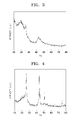
- FIG. 3 is a graph of X-ray diffraction results of carbide-derived carbon used.
- the peak of the graphite (002) surface is a peak generated by X-ray diffraction emitted in parallel with an upper surface of the hexagonal pillar.
- the carbide-derived carbon according to an embodiment of the present invention has amorphous properties unlike the conventional crystalline graphite.
- a full width at half maximum (FWHM) of the carbide-derived carbon is 6.6878°.
- FIG. 4 is a graph of X-ray diffraction results of a carbon nanotube hybrid system prepared from the carbide-derived carbon according to the inventive preparation method.
- the FWHM decreases to 0.89368°.
- Such change results from an increase of a degree of crystallinity as carbon nanotubes grow from the surfaces and pores of the carbide-derived carbon.
- a degree of crystallinity of the carbon nanotube hybrid system is greater than a degree of crystallinity of the carbide-derived carbon material used for preparation.
- FIG. 5 is a graph illustrating field emission results of a single wall carbon nanotube, a carbide-derived carbon, and a carbon nanotube hybrid system according to the present invention.
- a single wall carbon nanotube, a carbide-derived carbon, and a carbon nanotube hybrid system were respectively turned on at 1.5 V/ ⁇ m, 3.5 V/ ⁇ m, and 1.9 V/ ⁇ m, and respectively reached 700 ⁇ A/cm 2 at 2.5 V/ ⁇ m, 6.3 V/ ⁇ m, and 3.5 V/ ⁇ m
- emission efficiency of the carbon nanotube hybrid system is lower than the single wall carbon nanotube, the carbon nanotube hybrid system has sufficient emission efficiency for field emission applications, and the carbon nanotube hybrid system has excellent properties in uniform emission, Ohmic contact, lifetime, and the like.
- FIG. 6 is a graph illustrating lifetime of a carbon nanotube hybrid system compared to that of a single wall carbon nanotube.
- J-E loop aging (Target current density: 600 ⁇ A/cm 2 ) was conducted 60 times in a DC mode, and lifetimes of a single wall carbon nanotube and a carbon nanotube hybrid system according to an embodiment of the present invention were measured in a DC mode, and constant voltage mode.
- An initial current density was 100 ⁇ A/cm 2 (lo) and the lifetime was defined as time between the initial current density and a half-life, i.e., 50 ⁇ A/cm 2 ((1/2)I o ).
- the measured lifetime is different from the real lifetime of devices as the real devices operate in an AC mode and frequencies and pulse widths in the AC mode are different from those in the DC mode.
- the lifetime of the devices are measured in the DC mode so that a lifetime can be identified within a short time.
- the lifetime of the single wall carbon nanotube was about 6 hours
- the lifetime of the carbon nanotube hybrid system according to an embodiment of the present invention was about 46 hours, and thus has a 7.6 times improved lifetime characteristic.
- carbide compounds are reacted with a halogen group containing gas at a temperature in the range of 350 to 1600°C for 4 to 6 hours, and substantially all elements of the carbide compounds except carbons are extracted to prepare carbide-derived carbon.
- the content of elements other than carbon is at least less than 30 parts by weight, preferably, less than 20 parts by weight, most preferred less than 15 parts by weight, each based on 100 parts by weight of the carbide-derived carbon.
- the carbide compounds are carbon compounds may be carbides of Group III, IV, V, or VI element, and preferably, diamond-based carbide, such as SiC 4 or B 4 C; metal-based carbide, such as TiC or zirconium carbide; saline carbide, such as Al 4 C 3 or CaC 2 ; complex carbide, such as titanium tantalum carbide (TiTaC) or molybdenum tungsten carbide (MoWC); carbonitride, such as titanium carbonitride (TiNC) or zirconium carbonitride (ZrNC); or compounds thereof.
- the carbide compounds may include metals which can act as a catalyst for the growth of the carbon nanotubes.
- the halogen group containing gas may be Cl 2 , TiCl 4 , or F 2 .
- a catalyst metal-containing compound such as a metal halide, a metal nitrate, and the like, is added to the carbide-derived carbon and mixed, and a hydrogen reduction reaction is performed to obtain carbide-derived carbon on which metals are supported.
- the metal halide may be nickel halide, cobalt halide, iron halide, and tungsten halide.
- Metal nitrate perform similarly to the metal halide and may be nickel nitrate, cobalt nitrate, iron nitrate, and tungsten nitrate.
- the amount of the metal halide or the metal nitrate is in the range of 0.1 to 50 parts by weight based on 100 parts by weight of the carbide-derived carbon.
- the hydrogen reduction may be performed at a temperature in the range of 200 to 800°C.
- the (catalyst) metal may be a transition metal such as Ni, Co, Fe, or W, and the metal may be mixed with Mo to prevent catalyst agglomeration and decrease particle size of the catalyst to thereby improve efficiency.
- the (total) amount of the catalyst metals may be in the range of 0.1 to 20 parts by weight based on 100 parts by weight of the carbide-derived carbon.
- the prepared carbide-derived carbon is reacted with a carbon source in a high temperature synthesis furnace at a temperature in the range of 600 to 1200°C to obtain carbon nanotubes.
- a temperature in the range of 600 to 1200°C
- crystallinity may decrease due to a large amount of defect generated on the outside walls of the CNT.
- the temperature is higher than 1200°C, a uniform CNT cannot be obtained as the metal catalyst grows and a multi-wall nanotube having a large radius grows.
- Pores of the carbide-derived carbon may have a diameter in the range of 0.3 to 10 nm, and the pores may be micropores and mesopores.
- Carbide compounds more precisely carbide compounds of catalytic metals, are reacted with a halogen group containing gas at a temperature in the range of 350 to 1600°C, and elements of the carbide compounds, except carbon atoms, are partially extracted to prepare carbide-derived carbon.
- a halogen group containing gas at a temperature in the range of 350 to 1600°C
- elements of the carbide compounds, except carbon atoms are partially extracted to prepare carbide-derived carbon.
- catalytic metals remain in the carbide-derived carbon after the extraction step.
- the total amount of these catalyst metals in the carbide-derived carbon may be in the range of 0.1 to 20 parts by weight based on 100 parts by weight of the carbide-derived carbon.
- the halogen group containing gas is removed in a synthesis furnace by air purging the resultant, and then a carbon source is supplied to the synthesis furnace and reacted at a temperature in the range of 700 to 1200°C to obtain the carbon nanotube hybrid system.
- a carbon source is supplied to the synthesis furnace and reacted at a temperature in the range of 700 to 1200°C to obtain the carbon nanotube hybrid system.
- the temperature is less than 700°C, crystallinity may decrease due to a number defects on the outside walls of the CNT.
- the temperature is higher than 1200°C, a uniform CNT cannot be obtained since the metal catalyst grows and a multi-wall nanotube having a large radius grows.
- the carbon source may be ethylene gas, acetylene, a mixed gas of hydrogen and any one of the ethylene gas and acetylene, carbon monoxide, or the like.
- an electron emitter including the carbon nanotube hybrid system may be prepared.
- An electron emitter is an electron emitter for cold cathodes.
- the electron emitter emits electrons by photoelectric emission, electric field emission, or the like, wherein the electrons are generated by secondary electron emission and ion recombination by ion bombarding rather than being heated.
- the electron emitter includes the carbide-derived carbon according to aspects of the present invention having excellent electron emitting properties. Accordingly, the electron emitter has excellent electron emission efficiency.
- the electron emitter may be manufactured using a method, including preparing a composition for forming an electron emitter and applying and sintering the composition on a substrate, or the like.
- a composition for forming an electron emitter including the carbon nanotube hybrid system according to aspects of the present invention and a vehicle, is prepared.
- the vehicle adjusts printability and viscosity of the composition for forming the electron emitter, and includes a resin and a solvent component.
- the composition for forming the electron emitter may further include a photosensitive resin, a photoinitiator, an adhesive compound, a filler, etc.
- the substrate on which the electron emitter is formed may vary according to the type of electron emission device to be formed.
- the substrate may be the cathode.
- the application of the composition for forming the electron emitter to the substrate may vary according to whether photosensitive resins are included in the composition for forming the electron emitter.
- Additional photoresist patterns are unnecessary when the composition for forming the electron emitter includes photosensitive resins. That is, after coating the composition for forming the electron emitter including photosensitive resins on the substrate, the composition for forming the electron emitter is exposed and developed according to desired electron emitter forming regions. However, a photolithography process using additional photoresist patterns may be required when the composition for forming the electron emitter does not include photosensitive resins. That is, after photoresist patterns are formed on the substrate using a photoresist film, the composition for forming the electron emitter is applied to the substrate on which the photoresist patterns have been formed.
- the composition for forming the electron emitter applied to the substrate is sintered as described above.
- the adhesion between the carbide-derived carbon in the composition for forming the electron emitter and the substrate is increased due to the sintering.
- Many vehicles are volatilized and other inorganic binders, etc., are melted and solidified to enhance the durability of the electron emitter.
- the sintering temperature should be determined according to the volatilization temperature and volatilization time of the vehicle included in the composition for forming the electron emitter.
- the sintering may be performed in an inert gas atmosphere in order to inhibit degradation of the carbide-derived carbon.
- the inert gas may be nitrogen gas, argon gas, neon gas, xenon gas, or a mixture of at least two of the aforementioned gases.
- An activation process is alternatively performed on the surface of the sintered resultant.
- a solution which can be cured using heat treatment such as an electron emission source surface treatment material including a polyimide group polymer, is coated on the sintered resultant material and is heat treated. Then, the heat-treated film is delaminated.
- An adhesive part may be formed on the surface of a roller driving with a predetermined driving source, and an activating process is performed by applying predetermined pressure to a surface of the sintered resultant. Through this activating process, the carbon nanotube hybrid system can be exposed to a surface of the electron emitter or aligned vertically.
- an electron emission device including an electron emitter.
- Such an electron emission device includes a first substrate, a cathode and an electron emitter formed on the first substrate, a gate electrode arranged so as to be insulated electrically from the cathode, and an insulating layer arranged between the cathode and the gate electrode to insulate the cathode from the gate electrode.
- the electron emitter includes the carbon nanotube hybrid system.
- the electron emission device may further include a second insulating layer formed on an upper surface of the gate electrode to further insulate the gate electrode.
- the electron emission device is not limited thereto.
- the electron emission device may further include a focusing electrode arranged parallel with the gate electrode.
- the electron emission device may be used in a vacuum electric device such as a flat display, a television, an X line tube, an emission gate amplifier, or the like.
- FIG. 7 is a partial cross-sectional view illustrating an electron emission device 200 according to an embodiment of the present invention.
- the electron emission device 200 illustrated in FIG. 7 is a triode electron emission device, which is a representative electron emission device.
- the electron emission device 200 includes an upper plate 201 and a lower plate 202.
- the upper plate 201 includes an upper substrate 190, an anode electrode 180 formed on a lower surface 190a of the upper substrate 190, and a phosphor layer 170 formed on a lower surface 180a of the anode electrode 180.
- the lower plate 202 includes a lower substrate 110 formed opposite to the upper substrate 190 and parallel to the upper substrate 190 so that a predetermined interval is formed between the lower substrate 110 and the upper substrate 190, a stripe-type cathode electrode 120 formed on the lower substrate 110, a stripe-type gate electrode 140 formed to cross the cathode electrode 120, an insulating layer 130 formed between the gate electrode 140 and the cathode electrode 120, electron emitter holes 169 formed in the insulating layer 130 and gate electrode 140, and electron emitters 160 which are formed in the electron emitter holes 169 and electrically connected to the cathode electrode 120 to have a height lower than that of the gate electrode 140.
- the upper plate 201 and the lower plate 202 are maintained in position by a pressure lower than atmospheric pressure.
- a spacer 192 is formed between the upper plate 201 and the lower plate 202 so as to resist the pressure, which is generated by a vacuum, between the upper plate 201 and the lower plate 202 and to maintain an emission space 210.
- a high voltage is applied to the anode electrode 180 to accelerate electrons emitted from the electron emitters 160 so that they collide with the phosphor layer 170 at a high speed.
- the phosphor layer 170 is excited by the electrons and emits visible light as the energy of the electrons drops from a high energy level to a low energy level.
- the electron emission device 200 is a color electron emission device, phosphor layers, which emit red, green, and blue light into the emission space 210 forming a unit pixel, are formed on the lower surface 180a of the anode electrode 180.
- the gate electrode 140 enables electrons to be easily emitted from the electron emitters 160.
- the insulating layer 130 defines the electron emitter holes 169 and insulates the electron emitters 160 from the gate electrode 140.
- the electron emitters 160 which emit electrons by forming an electric field include the above described carbon nanotube hybrid system.
- Various carbon nanotube hybrid systems can be prepared using methods of preparing a carbon nanotube hybrid system. Further, the carbon nanotube hybrid system can be used not only as an electron emitter but as hydrogen storing material for fuel cells. Further, problems of entanglement and distribution which occur in conventional carbon nanotubes can be overcome by using the carbon nanotube hybrid system having cylindrical carbon nanotubes grown randomly from pores of CDC.
- the carbon nanotube hybrid system has excellent properties when in ohmic contact with a substrate and excellent uniformity when used as an electron emitter for an electron emission device and a material for a flat fluorescent lamp.
- An electron emitter device including the carbon nanotube hybrid system can be effectively used in a vacuum electric device such as a flat display, a television, an X line tube, an emission gate amplifier, or the like in addition to an electron emission device.
- carbide-derived carbon was prepared in the same manner as in Example 1 except that 100g of NiC having an average diameter of 3 ⁇ m was used as a starting carbide compound and was heat treated at 500°C for 2 hours.
- the carbide-derived carbon was analyzed using Raman peak analysis.
- the I G /I D ratio was about 1 to 1.3.
- the specific surface area of the carbide-derived carbon was 1200 m 2 /g.
- the amount of nickel in the carbide-derived carbon was 10.5 parts by weight based on 100 parts by weight of the total amount of the carbide-derived carbon and nickel.
- the resultant was purged with air to completely remove Cl 2 gas in the furnace, and ethylene gas was supplied to the furnace and reacted at 900°C to prepare a carbon nanotube hybrid system in which carbon nanotubes were grown from the carbide-derived carbon.
- 13g of carbide-derived carbon was prepared in the same manner as in Example 1 except that 100g of ZrC having an average diameter of 5 ⁇ m was used as a starting carbide compound and was heat treated at 600°C for 5 hours.
- the carbide-derived carbon was analyzed using Raman peak analysis.
- the I G /I D ratio was about 1 to 1.3.
- the specific surface area of the carbide-derived carbon (after synthesizing the carbide-derived carbon) was 1200 m 2 /g.
- a carbon nanotube hybrid system was prepared in the same manner as in Example 1 except that the carbide-derived carbon of Example 3 was used.
- Example 2 25g of carbide-derived carbon was prepared in the same manner as in Example 1 except that 100g of Al 4 C 3 having an average diameter (325 mesh powder) was used as a starting carbide compound and was heat treated at 700°C for 5 hours.
- a TEM image of the carbide-derived carbon is shown in FIG. 9 .
- the specific surface area of the carbide-derived carbon (after synthesizing the carbide-derived carbon) was in the range of 1050 to 1100 m 2 /g.
- a carbon nanotube hybrid system was prepared in the same manner as in Example 1 except that the carbide-derived carbon of Example 4 was used.
- Carbide-derived carbon was prepared in the same manner as in Example 1 except that 100g of B 4 C having an average diameter of 0.8 ⁇ m was used as a starting carbide compound and was heat treated at 1000°C for 3 hours.
- the carbide-derived carbon was analyzed using Raman peak analysis.
- the I G /I D ratio was about 0.4 to 1.
- As a result of a high resolution TEM analysis it was observed that amorphous openings were partially transformed into graphite fringes.
- a TEM image of the carbide-derived carbon is shown in FIG. 10 .
- the specific surface area of the carbide-derived carbon (after synthesizing the carbide-derived carbon) was 1310 m 2 /g.
- a carbon nanotube hybrid system was prepared in the same manner as in Example 1 except that the carbide-derived carbon of Example 5 was used.
- Table 1 briefly shows main properties of the carbide-derived carbon of Examples 1, and 3 through 5.
- Table 1 Example 1
- Example 3 Example 4
- Example 5 Starting carbide compound ⁇ -SiC ZrC Al 4 C 3 B 4 C Diameter of particle(1) ( ⁇ m) 0.7 5 10 0.8 Crystalline Structure (1) Hexagonal system Cubic system Trigonal system Trigonal system Main bond (1) Covalent bond Ionic bond Covalent bond Covalent bond Synthesizing temperature (2) (°C) 1000 600 700 1000 Synthesizing time (2) (hour) 7 5 5 5 3 Diameter of pore (nm) 0.7 0.6 ⁇ 1.2 1.5 4.0 Specific surface area of carbide-derived carbon (m 2 /g) 1000 ⁇ 1100 1200 1050 1310 Adsorption type of isothermal nitrogen I 3) I 3) I 3 ) IV 4) Volume of opening (cm 3 /cm 3 ) 0.58 0.64 0.86 0.75 Amount of carbide-derived carbon after halogenation (mass%) 29.8 13 25 20.8 I G /I D
- the resulting product was sintered under a nitrogen atmosphere at 450°C, and was activated to form cold cathodes.
- An electron emission device was manufactured using the electron emitter as cold cathodes, a polyethylene terephthalate film having a thickness of 100 ⁇ m as a spacer, and a copper plate as an anode plate.
- FIG. 5 is a graph illustrating field emission results of a carbon nanotube, a carbide-derived carbon, and a carbon nanotube hybrid system according to an embodiment of the present invention.
- a single wall carbon nanotube, a carbide-derived carbon, and a carbon nanotube hybrid system were respectively turned on at 1.5 V/ ⁇ m, 3.5 V/ ⁇ m, and 1.9 V/ ⁇ m and respectively reached 700 ⁇ A/cm 2 at 2.5 V/ ⁇ m, 6.3 V/ ⁇ m, and 3.5 V/ ⁇ m.
- emission efficiency of the carbon nanotube hybrid system is lower than the single wall carbon nanotube, the carbon nanotube hybrid system has sufficient emission efficiency for field emission applications and has excellent properties in uniform emission, Ohmic contact, lifetime, and the like.
- the carbon nanotube hybrid system according to aspects of the present invention has an excellent uniformity and a long lifetime.
- An electron emitter having improved electron emitting properties can be inexpensively prepared using the carbon nanotube hybrid system according to aspects of the present invention compared to conventional carbon nanotubes. Further, an electron emission device having excellent electron emitting properties can be prepared using the electron emitter according to aspects of the present invention.
Landscapes
- Engineering & Computer Science (AREA)
- Chemical & Material Sciences (AREA)
- Nanotechnology (AREA)
- Materials Engineering (AREA)
- Crystallography & Structural Chemistry (AREA)
- Manufacturing & Machinery (AREA)
- Organic Chemistry (AREA)
- General Physics & Mathematics (AREA)
- Condensed Matter Physics & Semiconductors (AREA)
- Physics & Mathematics (AREA)
- Composite Materials (AREA)
- Chemical Kinetics & Catalysis (AREA)
- Inorganic Chemistry (AREA)
- Carbon And Carbon Compounds (AREA)
- Cold Cathode And The Manufacture (AREA)
- Catalysts (AREA)
Abstract
Description
- Aspects of the present invention relate to a carbon nanotube hybrid system using carbide-derived carbon, an electron emitter including the same, and an electron emission device including the electron emitter, and more particularly, to a carbon nanotube hybrid system that can be prepared using a less expensive method than that used to manufacture conventional carbon nanotubes and that has excellent uniformity and a long lifetime, an electron emitter including the same, and an electron emission device including the electron emitter.
- In general, electron emission devices can be classified into electron emission devices using hot cathodes as an electron emission source and electron emission devices using cold cathodes as an electron emission source. Examples of electron emission devices using cold cathodes as an electron emission source include field emitter array (FEA) type electron emission devices, surface conduction emitter (SCE) type electron emission devices, metal insulator metal (MIM) type electron emission devices, metal insulator semiconductor (MIS) type electron emission devices, and ballistic electron surface emitting (BSE) type electron emission devices.
- FEA type electron emission devices operate based on a principle that a low work function material or high beta function material as an electron emission source easily emits electrons due to an electric potential difference under a vacuum condition. Recently, tip-shaped structures mainly formed of Mo, Si, or the like; carbonaceous material, such as graphite, diamond like carbon (DLC), or the like; and nano materials such as nanotubes, nanowires, or the like have been developed as electron emission sources for FEA type electron emission devices.
- In an SCE type electron emission device, a first electrode faces a second electrode on a first substrate, and a conductive thin film having fine cracks is located between the first and second electrodes. These fine cracks are used as an electron emission source. In this structure, when a voltage is applied to the device, current flows in the surface of the conductive thin film and electrons are emitted through the fine cracks acting as an electron emission source.
- MIM type electron emission devices and MIS type electron emission devices respectively include an electron emission source having a metal-dielectric layer-metal (MIM) structure and an electron emission source having a metal-dielectric layer-semiconductor structure. When a voltage is applied between the metals or between a metal and a semiconductor separated by a dielectric layer, electrons move, are accelerated, and are emitted from the metal or semiconductor having a higher electron charge to the metal having lower electron charge.
- BSE type electron emission devices operate based on a principle that when a semiconductor is miniaturized to a dimension smaller than a mean free path of the electrons of the semiconductor, electrons travel without being dispersed. In particular, an electron supply layer formed of a metal or a semiconductor is formed on an ohmic electrode, an insulating layer and a thin metal film are formed on the electron supply layer, and a voltage is applied to the ohmic electrode and the thin metal film to emit electrons.
- In addition, FEA type electron emission devices can be categorized into top gate type electron emission devices and bottom gate type electron emission devices according to locations of cathodes and gate electrodes. Furthermore, FEA type electron emission devices can be categorized into diode emission devices, triode electron emission devices, tetrode electron emission devices, etc., according to the number of electrodes used.
- In the electron emission devices described above, carbon-based materials, included in an emitter, for example, carbon nanotubes, which have good conductivity, electric field concentration, electric emission properties and a low work function, are commonly used.
- However, carbon nanotubes commonly have a fiber shape having a high field enhancement factor β, and fiber type carbon nanotube materials have many problems, such as poor uniformity and a short lifetime. Further, when fiber type carbon nanotubes are manufactured in a paste, an ink, a slurry, or the like, problems occur during manufacturing processes compared with other particle type materials, and raw materials of the fiber type carbon nanotubes are expensive.
- Recently, research on materials consisting of inexpensive carbide-based compounds that can be substituted for carbon nanotubes have been conducted in order to overcome these disadvantages (Korean Patent Publication No.
2001-13225 - The present invention provide a carbon nanotube hybrid system using carbide-derived carbon that can be prepared using a less expensive method than that used to manufacture conventional carbon nanotubes and that has excellent uniformity and a long lifetime, a method of preparing the same, an electron emitter including the carbon nanotube hybrid system, and an electron emission device including the electron emitter.
- According to an aspect of the present invention, there is provided a carbon nanotube hybrid system including: a carbide-derived carbon prepared by reacting a carbide compound and a halogen group containing gas to extract elements of the carbide compound except carbons; metals supported on the carbide-derived carbon or remaining in the carbide-derived carbon; and carbon nanotubes grown on the carbide-derived carbon from a supplied carbon source.
- According to another aspect of the present invention, there is provided a method of preparing a carbon nanotube hybrid system, the method including: extracting all elements of a carbide compound except carbon by reacting the carbide compound and a halogen group containing gas; mixing the carbide-derived carbon with a metal-containing compound and performing a hydrogen reduction reaction to transfer a metal from the metal-containing compound to the carbide-derived carbon; and reacting the prepared carbide-derived carbon and a carbon source to grow carbon nanotubes from the prepared carbide-derived carbon.
- According to another aspect of the present invention, there is provided a method of preparing a carbon nanotube hybrid system, the method including: extracting elements of a carbide compound except carbon by reacting the carbide compound and a halogen group containing gas, and reacting the resultant and a carbon source to grow carbon nanotubes from the prepared carbide-derived carbon.
- According to another aspect of the present invention, there is provided an electron emitter including the carbon nanotube hybrid system.
- According to another aspect of the present invention, there is provided an electron emission device comprising the electron emitter.
- According to another aspect of the invention, there is provided a method of preparing a carbon nanotube hybrid system. The method comprises the steps of:
- preparing a catalyst metal containing carbide-derived carbon material, wherein the catalyst metal is one being able to catalyze a growth of carbon nanotubes, said preparation step is performed by
- (i) providing a carbide compound; treating the carbide compound with a halogen containing gas thereby extracting substantially all elements of the carbide compound except carbon; and mixing the derived carbide-derived carbon material with a catalyst metal-containing compound and performing a hydrogen reduction reaction thereby depositing the catalyst metal from the catalyst metal-containing compound on a surface of the carbide-derived carbon material; or
- (ii) providing a carbide compound of the catalyst metal; and subsequent extracting the catalyst metal of the carbide compound in parts by reacting the carbide compound with a halogen containing gas; and,
- subsequent to preparation steps (i) or (ii), treating the prepared catalyst metal containing carbide-derived carbon material with a carbon source thereby growing carbon nanotubes on the surface of the surface of the prepared carbide-derived carbon material.
- According to another aspect of the present invention, there is provided a carbon nanotube hybrid system which has been prepared according to the before mentioned preparation method. The carbon nanotube hybrid system includes: a carbide-derived carbon material (prepared by reacting a carbide compound and a halogen containing gas to extract elements of the carbide compound except carbons); metals supported on the carbide-derived carbon material or remaining in the carbide-derived carbon; and carbon nanotubes grown on the carbide-derived carbon material.
- Additional aspects and/or advantages of the invention will be set forth in part in the description which follows and, in part, will be obvious from the description, or may be learned by practice of the invention.
- These and/or other aspects and advantages of the invention will become apparent and more readily appreciated from the following description of the embodiments, taken in conjunction with the accompanying drawings of which:
-
FIG. 1A is a transmission electron microscope (TEM) image of a surface of a carbide-derived carbon on which a metal catalyst is supported in the initial stage of a synthesis of a carbon nanotube hybrid system according to an embodiment of the present invention; -
FIG. 1B is a TEM image illustrating a carbon nanotube hybrid system according to an embodiment of the present invention; -
FIG. 1C is a scanning emission microscope (SEM) image illustrating a carbon nanotube hybrid system according to an embodiment of the present invention; -
FIG. 1D is a schematic diagram illustrating a nano structure of a conventional carbide-derived carbon; -
FIG. 2A is a graph of Raman peak analysis results of a carbide-derived carbon according to an embodiment of the present invention; -
FIG. 2B is a graph of Raman peak analysis results of a carbon nanotube hybrid system according to an embodiment of the present invention; -
FIG. 3 is a graph of X-ray diffraction results of carbide-derived carbon according to an embodiment of the present invention; -
FIG. 4 is a graph of X-ray diffraction results of a carbon nanotube hybrid system according to an embodiment of the present invention; -
FIG. 5 is a graph illustrating field emission results of a carbon nanotube, a carbide-derived carbon and a carbon nanotube hybrid system according to an embodiment of the present invention; -
FIG. 6 is a graph illustrating lifetime of a carbon nanotube hybrid system compared to that of a carbon nanotube according to an embodiment of the present invention; -
FIG. 7 is a partial cross-sectional view of an electron emitter according to an embodiment of the present invention; -
FIGS. 8 and9 are TEM images of a carbide-derived carbon after synthesizing Al4C3 according to Example 4; and -
FIG. 10 is a TEM image of carbide-derived carbon after synthesizing B4C according to Example 5. - Reference will now be made in detail to the present embodiments of the present invention, examples of which are illustrated in the accompanying drawings, wherein like reference numerals refer to the like elements throughout. The embodiments are described below in order to explain the aspects of present invention by referring to the figures.
- A carbon nanotube hybrid system according to aspects of the present invention can be prepared by reacting the following: a carbide-derived carbon (prepared by reacting carbide compounds) and a halogen group containing gas to extract all elements of the carbide compounds except carbons; metals supported on the carbide-derived carbon, particularly on at least one of pores and surfaces of the carbide-derived carbon (preferably on both of pores and surfaces of the carbide-derived carbon) or remaining in the carbide-derived carbon; and carbon sources. The carbon nanotube hybrid system has a structure in which carbon nanotubes are grown from the carbide-derived carbon, particularly from at least one of pores and surfaces of the carbide-derived carbon (preferably from both of pores and surfaces of the carbide-derived carbon). The carbon nanotube hybrid system can be inexpensively prepared, have excellent electron emitting properties, and be used to prepare an electron emitter having excellent electron emitting properties and an electron emission device including the electron emitter.
- The metals supported on pores and surfaces of the carbide-derived carbon or remaining in the carbide-derived carbon are catalyst metals that can assist the growth of the carbon nanotubes. The catalyst metals have nanosize particles, and more particularly, a particle size distribution in the range of a sub-nanometer scale, i.e., a particle size of less than 1 nm to a nanometer scale particle size.
- A radius of the carbon nanotube (CNT) is determined according to the particle size range of the catalyst metals, and thus fine CNT can be obtained using the catalyst metals having a small particle size distribution. The catalyst metals may have a particle size distribution in the range of a sub-nanometer to 5 nm. When those catalyst metals are supported on the carbide derived carbon, a single-walled nanotube (SWNT), double-walled nanotube (DWNT), or thin multi-walled nanotube (thin-MWNT) can be prepared having a thickness of less than or equal to several nanometers, but such thickness can be varied according to types of carbon sources, synthesis temperature, and synthesis time. Particularly, a carbon nanotube hybrid system having 10 walls or less and a diameter of 20 nm or less may be formed. Further, a carbon nanotube hybrid system having MWNT which grow from a carbide-derived carbon when C2H2 gas is used as the carbon source of the carbon nanotube hybrid system can be prepared.
-
FIG. 1A is a transmission electron microscopy (TEM) image of a surface of a carbide-derived carbon on which a metal catalyst is supported in the initial stage of a synthesis of a carbon nanotube hybrid system. A carbon layer grows from the supported catalyst.FIG. 1B is a TEM image illustrating a carbon nanotube hybrid system according to an embodiment of the present invention. As shown inFIG. 1A , a multi-walled carbon nanotube grows from the surface of carbide-derived carbon on which the metal catalyst is supported. - The CNTs may grow perpendicularly to the substrate. When the carbon nanotube hybrid system having such structure is used as an electron emitter, excellent electron emitting properties are obtained as well as uniform electron emission may be induced by ohmic contact with a lower electrode. Tips of the CNTs may have a needle shape as illustrated in
FIG. 1B to provide a field enhancement factor (β-factor). - Carbide-derived carbon may be prepared by reacting carbide compounds and a halogen group containing gas to extract (substantially) all elements of the carbide compounds except carbons. As disclosed in Korean Patent Publication No.
2001-13225 - When the carbide-derived carbon prepared using the above method is analyzed using Raman peaks, the carbide-derived carbon has preferably intensity ratios of a graphite G band at 1590cm-1 to a disordered-induced D band at 1350cm-1 is in the range of 0.3 to 5, or a BET surface area of 950 m2/g, preferably 950-1400 m2/g. When the carbide-derived carbon is analyzed using X-ray diffraction, a weak or wide single peak of a graphite (002) surface can be seen at 2θ = 25°. The carbide-derived carbon prepared using the above method has a q value indicating a degree of crystallinity in the range of 0 to 60.
- Generally, results of analysis of the Raman peaks, X-ray diffraction and electron microscopy are commonly used as criteria to indicate degrees of crystallinity. The carbide-derived carbon used has a structure that has a degree of crystallinity in a short range order and is similar to that of amorphous carbon as determined as described above. It has been documented that amorphous carbon having a degree of crystallinity in a short range order has a structure where bending graphite sheets and open pores, including non-6-memered rings, are mixed (Enn Lust et al., J. Electroanalytical Chem., vol. 586, pp 247, 2006).
FIG. 1D is a view illustrating a nanostructure of amorphous carbon disclosed in the above reference. Carbide-derived carbon having such structure as illustrated inFIG. 1D and has excellent electron emitting properties. The nanostructure of the carbide-derived carbon emits fields from open pores, having a structure of a non-6-membered ring, and the open pores are perpendicular to a surface of the carbide-derived carbon. -
FIG. 2A is a graph of Raman peak analysis results of a carbide-derived carbon used (514.532 nm, D1 filter, Ar ion). Referring toFIG. 2A , the carbide-derived carbon has an intensity ratio (IG/ID) of a graphite G band at 1590cm-1 to a disordered-induced D band at 1350cm-1 of about 0.76. -
FIG. 2B is a graph of Raman peak analysis results of a carbon nanotube hybrid system prepared from the carbide-derived carbon ofFIG. 2A using the inventive method (514.532 nm, D1 filter, Ar ion). Referring toFIG. 2B , the intensity of the graphite G band at 1590cm-1 the carbon nanotube hybrid system increases compared to that of the carbide-derived carbon ofFIG. 2A . Further, the intensity ratio (IG/ID) of a graphite G band at 1590cm-1 to a disordered-induced D band at 1350cm-1 increased to about 2.46. In addition, it is identified that SWNT grow from pores and surfaces of the carbide-derived carbon as indicated by radial breathing mode (RBM) peaks generated at 164.03, 212.01, 270.75cm-1, and the like which are related to curvature of SWNT. Analyzer used in such Raman peak analysis is HORIBA 800UV commercially available from HORIBAJOBINYVON. The Raman peak analysis was performed using an internal laser (Ar). The laser has an output of 20-30 mW, and a wavelength of 514.5nm. Exposing time of the laser is 120 sec, and a size of beam hole is 100µm. Hence, an intensity ratio of a graphite G band at 1590cm-1 to a disordered-induced D band at 1350cm-1 of the carbon nanotube hybrid system is greater than an intensity ratio of a graphite G band at 1590cm-1 to a disordered-induced D band at 1350cm-1 of the carbide-derived carbon material used for preparation. -
FIG. 3 is a graph of X-ray diffraction results of carbide-derived carbon used. Referring toFIG. 3 , in the carbide-derived carbon, a weak peak of a graphite (002) surface can be seen at 2θ = 25.9°. When a crystal structure of graphite is a hexagonal pillar, the peak of the graphite (002) surface is a peak generated by X-ray diffraction emitted in parallel with an upper surface of the hexagonal pillar. Typically, a very strong peak of the conventional crystalline graphite can be seen at 2θ = 25°. However, a very weak peak of the carbide-derived carbon can be seen at 2θ = 25°. Accordingly, the carbide-derived carbon according to an embodiment of the present invention has amorphous properties unlike the conventional crystalline graphite. Further, a full width at half maximum (FWHM) of the carbide-derived carbon is 6.6878°. -
FIG. 4 is a graph of X-ray diffraction results of a carbon nanotube hybrid system prepared from the carbide-derived carbon according to the inventive preparation method. Referring toFIG. 4 , the FWHM decreases to 0.89368°. Such change results from an increase of a degree of crystallinity as carbon nanotubes grow from the surfaces and pores of the carbide-derived carbon. Hence, a degree of crystallinity of the carbon nanotube hybrid system is greater than a degree of crystallinity of the carbide-derived carbon material used for preparation. -
FIG. 5 is a graph illustrating field emission results of a single wall carbon nanotube, a carbide-derived carbon, and a carbon nanotube hybrid system according to the present invention. A single wall carbon nanotube, a carbide-derived carbon, and a carbon nanotube hybrid system were respectively turned on at 1.5 V/µm, 3.5 V/µm, and 1.9 V/µm, and respectively reached 700 µA/cm2 at 2.5 V/µm, 6.3 V/µm, and 3.5 V/µm Although emission efficiency of the carbon nanotube hybrid system is lower than the single wall carbon nanotube, the carbon nanotube hybrid system has sufficient emission efficiency for field emission applications, and the carbon nanotube hybrid system has excellent properties in uniform emission, Ohmic contact, lifetime, and the like. -
FIG. 6 is a graph illustrating lifetime of a carbon nanotube hybrid system compared to that of a single wall carbon nanotube. J-E loop aging (Target current density: 600 µA/cm2) was conducted 60 times in a DC mode, and lifetimes of a single wall carbon nanotube and a carbon nanotube hybrid system according to an embodiment of the present invention were measured in a DC mode, and constant voltage mode. An initial current density was 100 µA/cm2 (lo) and the lifetime was defined as time between the initial current density and a half-life, i.e., 50 µA/cm2 ((1/2)Io). The measured lifetime is different from the real lifetime of devices as the real devices operate in an AC mode and frequencies and pulse widths in the AC mode are different from those in the DC mode. However, the lifetime of the devices are measured in the DC mode so that a lifetime can be identified within a short time. Referring toFIG. 6 , while the lifetime of the single wall carbon nanotube was about 6 hours, the lifetime of the carbon nanotube hybrid system according to an embodiment of the present invention was about 46 hours, and thus has a 7.6 times improved lifetime characteristic. - Hereinafter, methods of preparing a carbon nanotube hybrid system will be described. In a first method of preparing the hybrid system, carbide compounds are reacted with a halogen group containing gas at a temperature in the range of 350 to 1600°C for 4 to 6 hours, and substantially all elements of the carbide compounds except carbons are extracted to prepare carbide-derived carbon. After the step of extracting, the content of elements other than carbon is at least less than 30 parts by weight, preferably, less than 20 parts by weight, most preferred less than 15 parts by weight, each based on 100 parts by weight of the carbide-derived carbon.
- The carbide compounds are carbon compounds may be carbides of Group III, IV, V, or VI element, and preferably, diamond-based carbide, such as SiC4 or B4C; metal-based carbide, such as TiC or zirconium carbide; saline carbide, such as Al4C3 or CaC2; complex carbide, such as titanium tantalum carbide (TiTaC) or molybdenum tungsten carbide (MoWC); carbonitride, such as titanium carbonitride (TiNC) or zirconium carbonitride (ZrNC); or compounds thereof. The carbide compounds may include metals which can act as a catalyst for the growth of the carbon nanotubes. The halogen group containing gas may be Cl2, TiCl4, or F2.
- Then, a catalyst metal-containing compound, such as a metal halide, a metal nitrate, and the like, is added to the carbide-derived carbon and mixed, and a hydrogen reduction reaction is performed to obtain carbide-derived carbon on which metals are supported. The metal halide may be nickel halide, cobalt halide, iron halide, and tungsten halide. Metal nitrate perform similarly to the metal halide and may be nickel nitrate, cobalt nitrate, iron nitrate, and tungsten nitrate. The amount of the metal halide or the metal nitrate is in the range of 0.1 to 50 parts by weight based on 100 parts by weight of the carbide-derived carbon.
- The hydrogen reduction may be performed at a temperature in the range of 200 to 800°C. The (catalyst) metal may be a transition metal such as Ni, Co, Fe, or W, and the metal may be mixed with Mo to prevent catalyst agglomeration and decrease particle size of the catalyst to thereby improve efficiency. The (total) amount of the catalyst metals may be in the range of 0.1 to 20 parts by weight based on 100 parts by weight of the carbide-derived carbon.
- The prepared carbide-derived carbon is reacted with a carbon source in a high temperature synthesis furnace at a temperature in the range of 600 to 1200°C to obtain carbon nanotubes. When the temperature is less than 700°C, crystallinity may decrease due to a large amount of defect generated on the outside walls of the CNT. On the other hand, when the temperature is higher than 1200°C, a uniform CNT cannot be obtained as the metal catalyst grows and a multi-wall nanotube having a large radius grows. Pores of the carbide-derived carbon may have a diameter in the range of 0.3 to 10 nm, and the pores may be micropores and mesopores.
- A second method of preparing carbon nanotubes according to an embodiment of the present invention will now be described. Carbide compounds, more precisely carbide compounds of catalytic metals, are reacted with a halogen group containing gas at a temperature in the range of 350 to 1600°C, and elements of the carbide compounds, except carbon atoms, are partially extracted to prepare carbide-derived carbon. Thus, catalytic metals remain in the carbide-derived carbon after the extraction step. Here, the total amount of these catalyst metals in the carbide-derived carbon may be in the range of 0.1 to 20 parts by weight based on 100 parts by weight of the carbide-derived carbon.
- The halogen group containing gas is removed in a synthesis furnace by air purging the resultant, and then a carbon source is supplied to the synthesis furnace and reacted at a temperature in the range of 700 to 1200°C to obtain the carbon nanotube hybrid system. When the temperature is less than 700°C, crystallinity may decrease due to a number defects on the outside walls of the CNT. On the other hand, when the temperature is higher than 1200°C, a uniform CNT cannot be obtained since the metal catalyst grows and a multi-wall nanotube having a large radius grows.
- In the second method, types and amounts of the carbide compounds, the halogen group containing gas, and carbon source are similar to those used in the first method. The carbon source may be ethylene gas, acetylene, a mixed gas of hydrogen and any one of the ethylene gas and acetylene, carbon monoxide, or the like.
- Aspects of the present invention also provide that an electron emitter including the carbon nanotube hybrid system may be prepared.
- An electron emitter according to an embodiment of the present invention is an electron emitter for cold cathodes. The electron emitter emits electrons by photoelectric emission, electric field emission, or the like, wherein the electrons are generated by secondary electron emission and ion recombination by ion bombarding rather than being heated. In addition, the electron emitter includes the carbide-derived carbon according to aspects of the present invention having excellent electron emitting properties. Accordingly, the electron emitter has excellent electron emission efficiency.
- The electron emitter may be manufactured using a method, including preparing a composition for forming an electron emitter and applying and sintering the composition on a substrate, or the like.
- First, a composition for forming an electron emitter, including the carbon nanotube hybrid system according to aspects of the present invention and a vehicle, is prepared. The vehicle adjusts printability and viscosity of the composition for forming the electron emitter, and includes a resin and a solvent component. In addition, the composition for forming the electron emitter may further include a photosensitive resin, a photoinitiator, an adhesive compound, a filler, etc.
- Next, the composition for forming the electron emitter is applied to the substrate. The substrate on which the electron emitter is formed may vary according to the type of electron emission device to be formed. For example, when manufacturing an electron emission device with gate electrodes between a cathode and an anode, the substrate may be the cathode.
- The application of the composition for forming the electron emitter to the substrate may vary according to whether photosensitive resins are included in the composition for forming the electron emitter.
- Additional photoresist patterns are unnecessary when the composition for forming the electron emitter includes photosensitive resins. That is, after coating the composition for forming the electron emitter including photosensitive resins on the substrate, the composition for forming the electron emitter is exposed and developed according to desired electron emitter forming regions. However, a photolithography process using additional photoresist patterns may be required when the composition for forming the electron emitter does not include photosensitive resins. That is, after photoresist patterns are formed on the substrate using a photoresist film, the composition for forming the electron emitter is applied to the substrate on which the photoresist patterns have been formed.
- The composition for forming the electron emitter applied to the substrate is sintered as described above. The adhesion between the carbide-derived carbon in the composition for forming the electron emitter and the substrate is increased due to the sintering. Many vehicles are volatilized and other inorganic binders, etc., are melted and solidified to enhance the durability of the electron emitter. The sintering temperature should be determined according to the volatilization temperature and volatilization time of the vehicle included in the composition for forming the electron emitter. The sintering may be performed in an inert gas atmosphere in order to inhibit degradation of the carbide-derived carbon. The inert gas may be nitrogen gas, argon gas, neon gas, xenon gas, or a mixture of at least two of the aforementioned gases.
- An activation process is alternatively performed on the surface of the sintered resultant. According to an embodiment of the present invention, a solution which can be cured using heat treatment, such as an electron emission source surface treatment material including a polyimide group polymer, is coated on the sintered resultant material and is heat treated. Then, the heat-treated film is delaminated. An adhesive part may be formed on the surface of a roller driving with a predetermined driving source, and an activating process is performed by applying predetermined pressure to a surface of the sintered resultant. Through this activating process, the carbon nanotube hybrid system can be exposed to a surface of the electron emitter or aligned vertically.
- Aspects of the present invention also provide for an electron emission device including an electron emitter. Such an electron emission device includes a first substrate, a cathode and an electron emitter formed on the first substrate, a gate electrode arranged so as to be insulated electrically from the cathode, and an insulating layer arranged between the cathode and the gate electrode to insulate the cathode from the gate electrode. Here, the electron emitter includes the carbon nanotube hybrid system.
- The electron emission device may further include a second insulating layer formed on an upper surface of the gate electrode to further insulate the gate electrode. However, the electron emission device is not limited thereto. For example, as the gate electrode is insulated by the second insulating layer, the electron emission device may further include a focusing electrode arranged parallel with the gate electrode. The electron emission device may be used in a vacuum electric device such as a flat display, a television, an X line tube, an emission gate amplifier, or the like.
-
FIG. 7 is a partial cross-sectional view illustrating anelectron emission device 200 according to an embodiment of the present invention. Theelectron emission device 200 illustrated inFIG. 7 is a triode electron emission device, which is a representative electron emission device. - Referring to
FIG. 7 , theelectron emission device 200 includes anupper plate 201 and alower plate 202. Theupper plate 201 includes anupper substrate 190, ananode electrode 180 formed on alower surface 190a of theupper substrate 190, and aphosphor layer 170 formed on a lower surface 180a of theanode electrode 180. - The
lower plate 202 includes alower substrate 110 formed opposite to theupper substrate 190 and parallel to theupper substrate 190 so that a predetermined interval is formed between thelower substrate 110 and theupper substrate 190, a stripe-type cathode electrode 120 formed on thelower substrate 110, a stripe-type gate electrode 140 formed to cross thecathode electrode 120, an insulatinglayer 130 formed between thegate electrode 140 and thecathode electrode 120, electron emitter holes 169 formed in the insulatinglayer 130 andgate electrode 140, andelectron emitters 160 which are formed in the electron emitter holes 169 and electrically connected to thecathode electrode 120 to have a height lower than that of thegate electrode 140. - The
upper plate 201 and thelower plate 202 are maintained in position by a pressure lower than atmospheric pressure. Aspacer 192 is formed between theupper plate 201 and thelower plate 202 so as to resist the pressure, which is generated by a vacuum, between theupper plate 201 and thelower plate 202 and to maintain anemission space 210. - A high voltage is applied to the
anode electrode 180 to accelerate electrons emitted from theelectron emitters 160 so that they collide with thephosphor layer 170 at a high speed. Thephosphor layer 170 is excited by the electrons and emits visible light as the energy of the electrons drops from a high energy level to a low energy level. When theelectron emission device 200 is a color electron emission device, phosphor layers, which emit red, green, and blue light into theemission space 210 forming a unit pixel, are formed on the lower surface 180a of theanode electrode 180. - The
gate electrode 140 enables electrons to be easily emitted from theelectron emitters 160. The insulatinglayer 130 defines the electron emitter holes 169 and insulates theelectron emitters 160 from thegate electrode 140. - The
electron emitters 160 which emit electrons by forming an electric field include the above described carbon nanotube hybrid system. - Various carbon nanotube hybrid systems can be prepared using methods of preparing a carbon nanotube hybrid system. Further, the carbon nanotube hybrid system can be used not only as an electron emitter but as hydrogen storing material for fuel cells. Further, problems of entanglement and distribution which occur in conventional carbon nanotubes can be overcome by using the carbon nanotube hybrid system having cylindrical carbon nanotubes grown randomly from pores of CDC.
- The carbon nanotube hybrid system has excellent properties when in ohmic contact with a substrate and excellent uniformity when used as an electron emitter for an electron emission device and a material for a flat fluorescent lamp. An electron emitter device including the carbon nanotube hybrid system can be effectively used in a vacuum electric device such as a flat display, a television, an X line tube, an emission gate amplifier, or the like in addition to an electron emission device.
- Aspects of the present invention will now be described in further detail with reference to the following examples.
- 100g of α-SiC having an average diameter of 0.7µm as a carbon precursor (carbide compound) was maintained in a high temperature furnace composed of a graphite reaction chamber, a transformer, and the like. 0.5 L of CI2 gas was applied to the high temperature furnace at 1000°-C per minute for 7 hours. Thereby, 30g of carbide-derived carbon was prepared by extracting the Si from the carbon precursor.
- The carbide-derived carbon was analyzed using Raman peak analysis, X-ray diffraction, and an electron microscope. As a result, the IG/ID ratio was about 0.5 to 1. A weak peak of a graphite (002) surface could be seen at 2θ = 25°, and the electron diffraction pattern was a halo-pattern of amorphous carbon. Further, the specific surface area of the carbide-derived carbon was 1000 to 1100 m2/g.
- 20g of the carbide-derived carbon was mixed with 2g of iron (III) nitrate (Fe(NO3)3) in an ethanol solution, the mixture was filtered and a hydrogen reduction reaction was performed to prepare a carbon nanotube hybrid system in which carbon nanotubes were grown from the carbide-derived carbon. Raman spectrum of the prepared the carbon nanotube hybrid system was shown in
FIG. 2B , and an XRD pattern thereof is shown inFIG. 4 . - 9.5g of carbide-derived carbon was prepared in the same manner as in Example 1 except that 100g of NiC having an average diameter of 3µm was used as a starting carbide compound and was heat treated at 500°C for 2 hours. The carbide-derived carbon was analyzed using Raman peak analysis. The IG/ID ratio was about 1 to 1.3. A wide single peak of a graphite (002) surface could be seen at 2θ = 25° using the X-ray diffraction. In addition, the specific surface area of the carbide-derived carbon was 1200 m2/g.
- The amount of nickel in the carbide-derived carbon was 10.5 parts by weight based on 100 parts by weight of the total amount of the carbide-derived carbon and nickel.
- The resultant was purged with air to completely remove Cl2 gas in the furnace, and ethylene gas was supplied to the furnace and reacted at 900°C to prepare a carbon nanotube hybrid system in which carbon nanotubes were grown from the carbide-derived carbon.
- 13g of carbide-derived carbon was prepared in the same manner as in Example 1 except that 100g of ZrC having an average diameter of 5µm was used as a starting carbide compound and was heat treated at 600°C for 5 hours. The carbide-derived carbon was analyzed using Raman peak analysis. The IG/ID ratio was about 1 to 1.3. A wide single peak of a graphite (002) surface could be seen at 2θ = 25° using the X-ray diffraction. In addition, the specific surface area of the carbide-derived carbon (after synthesizing the carbide-derived carbon) was 1200 m2/g.
- A carbon nanotube hybrid system was prepared in the same manner as in Example 1 except that the carbide-derived carbon of Example 3 was used.
- 25g of carbide-derived carbon was prepared in the same manner as in Example 1 except that 100g of Al4C3 having an average diameter (325 mesh powder) was used as a starting carbide compound and was heat treated at 700°C for 5 hours. The carbide-derived carbon was analyzed using Raman peak analysis. The IG/ID ratio was about 1 to 3.2. A wide single peak of a graphite (002) surface could be seen at 2θ = 25° using the X-ray diffraction. As a result of a high resolution TEM analysis, a plurality of graphite fringes was observed. A TEM image of the carbide-derived carbon is shown in
FIG. 9 . In addition, the specific surface area of the carbide-derived carbon (after synthesizing the carbide-derived carbon) was in the range of 1050 to 1100 m2/g. - A carbon nanotube hybrid system was prepared in the same manner as in Example 1 except that the carbide-derived carbon of Example 4 was used.
- Carbide-derived carbon was prepared in the same manner as in Example 1 except that 100g of B4C having an average diameter of 0.8µm was used as a starting carbide compound and was heat treated at 1000°C for 3 hours. The carbide-derived carbon was analyzed using Raman peak analysis. The IG/ID ratio was about 0.4 to 1. A weak peak of a graphite (002) surface could be seen at 2θ = 25° using the X-ray diffraction. As a result of a high resolution TEM analysis, it was observed that amorphous openings were partially transformed into graphite fringes. A TEM image of the carbide-derived carbon is shown in
FIG. 10 . In addition, the specific surface area of the carbide-derived carbon (after synthesizing the carbide-derived carbon) was 1310 m2/g. - A carbon nanotube hybrid system was prepared in the same manner as in Example 1 except that the carbide-derived carbon of Example 5 was used.
- Table 1 briefly shows main properties of the carbide-derived carbon of Examples 1, and 3 through 5.
Table 1 Example 1 Example 3 Example 4 Example 5 Starting carbide compound α-SiC ZrC Al4C3 B4C Diameter of particle(1) (µm) 0.7 5 10 0.8 Crystalline Structure(1) Hexagonal system Cubic system Trigonal system Trigonal system Main bond(1) Covalent bond Ionic bond Covalent bond Covalent bond Synthesizing temperature (2) (°C) 1000 600 700 1000 Synthesizing time(2) (hour) 7 5 5 3 Diameter of pore (nm) 0.7 0.6 ~ 1.2 1.5 4.0 Specific surface area of carbide-derived carbon (m2/g) 1000~1100 1200 1050 1310 Adsorption type of isothermal nitrogen I3) I3) I3) IV4) Volume of opening (cm3/cm3) 0.58 0.64 0.86 0.75 Amount of carbide-derived carbon after halogenation (mass%) 29.8 13 25 20.8 IG/ID ratio 0.5 ~ 1 1 ~ 1.3 1 ~ 3.2 0.4 ~ 1 Turn-on electric field (V/µm)(4) 6 ~ 12 @1/500 duty ratio 12 ~ 14 @1/140 duty ratio(5) 8 ~ 13 @1/140 duty ratio(5) 10 ~ 13 @1/500 duty ratio Electric field emission properties 100 µA/cm2@10~1 3 V/µm 100 µA/cm2@14~1 7 V/µm 100 µA/cm2@12~1 5 V/µm 100 µA/cm2@13~1 6 V/µm 1) property of a carbide compound as a starting material (a diameter of a particle of a starting carbide compound is not varied even after preparing carbide-derived carbon)
2) synthesizing condition of carbide-derived carbon
3) type where adsorption occurs irrespective of a pressure of a gas, an intensity of adsorption is great and adsorption occurs at a specific point
4) type where a capillary condensation phenomenon at a middle opening and a desorption curve is higher than an adsorption curve irrespective of a relative pressure
5) Electrons are not emitted at a 1/500 duty ratio, but are emitted at a 1/140 duty ratio - Physical properties and electric field emission properties of the carbide-derived carbon of Examples 1 and 3 through 5, similar Raman IG/ID ratios, XRD patterns, and TEM morphologies were observed, but differences of electron emission performance were observed. Carbide-derived carbon has different properties and electric field emission efficiencies according to synthesizing conditions although the same carbide compounds were used as a starting material. Different electric field emission properties can be observed according to the kinds of starting materials since a distance between carbon and carbon, distribution of crystalloids, and diameter and volume of openings of an amorphous material of carbide-derived carbon after synthesis are varied although carbide-derived carbon is synthesized under the same synthesizing conditions. However, carbide-derived carbon materials in which electric field emission can occur at a duty ratio greater than 1/140 include carbide-derived carbon whose intensity ratios of graphite G band at 1590cm-1 to a disordered-induced D band at 1350cm-1 are in the range of 0.3 through 5 when the carbide-derived carbon is analyzed using Raman peak analysis; carbon having a specific surface area of 950 m2/g and more; carbide-derived carbon in which a weak or wide single peak of a graphite (002) surface can be observed at 2θ = 25° when analyzing the carbide-derived carbon using X-ray diffraction; and carbide-derived carbon where an electron diffraction pattern is a halo-pattern of amorphous carbon when analyzing the carbide-derived carbon using electron microscopy.
- As shown in Table 1, electric field emission properties of carbon nanotube hybrid systems prepared according to Examples 1 and 3 through 5 were measured. As a result, it was shown that the carbon nanotube hybrid systems had excellent electric field emission properties.
- 1 g of the carbon nanotube hybrid system prepared in Example 1, 6.5g of an acrylate binder, 5.5g of ethoxylate trimethylolpropane triacrylate, 5.5g of texanol, 1 g of a photoinitiator and 1g of di-octyl phthalate 1g as a plasticizer were mixed, and were dispersed using a 3-roll mill until a well-mixed composition for forming an electron emitter was obtained (repeated 8 times). Screen printing was used to apply the obtained composition to a transparent glass substrate on which an ITO electrode was coated (10x10mm), and the composition was exposed (at 500mJ) and developed. Next, the resulting product was sintered under a nitrogen atmosphere at 450°C, and was activated to form cold cathodes. An electron emission device was manufactured using the electron emitter as cold cathodes, a polyethylene terephthalate film having a thickness of 100µm as a spacer, and a copper plate as an anode plate.
- The emission current density of the manufactured electron emission device was measured by applying a pulse voltage at a duty ratio of 1/500 having a pulse width of 20µs and a frequency of 100Hz. As a result, the electron emission device using the carbon nanotube hybrid system according to Example 1 had excellent electron emitting properties.
FIG. 5 is a graph illustrating field emission results of a carbon nanotube, a carbide-derived carbon, and a carbon nanotube hybrid system according to an embodiment of the present invention. A single wall carbon nanotube, a carbide-derived carbon, and a carbon nanotube hybrid system were respectively turned on at 1.5 V/µm, 3.5 V/µm, and 1.9 V/µm and respectively reached 700 µA/cm2 at 2.5 V/µm, 6.3 V/µm, and 3.5 V/µm. Although emission efficiency of the carbon nanotube hybrid system is lower than the single wall carbon nanotube, the carbon nanotube hybrid system has sufficient emission efficiency for field emission applications and has excellent properties in uniform emission, Ohmic contact, lifetime, and the like. - A similar experiment to measure performance was conducted in the other electron emission devices using the other carbide nanotube hybrid systems. As a result, the other electron emission devices were found to have similar electron emission properties as the electron emission device using the carbon nanotube hybrid system according to Example 1.
- The carbon nanotube hybrid system according to aspects of the present invention has an excellent uniformity and a long lifetime. An electron emitter having improved electron emitting properties can be inexpensively prepared using the carbon nanotube hybrid system according to aspects of the present invention compared to conventional carbon nanotubes. Further, an electron emission device having excellent electron emitting properties can be prepared using the electron emitter according to aspects of the present invention.
Claims (18)
- A carbon nanotube hybrid system, comprising:carbide-derived carbon formed by reacting a carbide compound and a halogen group containing gas to extract elements of the carbide compound except carbon;a metal supported on the carbide-derived carbon; andcarbon nanotubes grown on the carbide-derived carbon from a supplied carbon source.
- The carbon nanotube hybrid system of claim 1, wherein the metal is at least one of Ni, Co, Fe, or W in an amount of 0.1 to 20 parts by weight based on 100 parts by weight of the total amount of the metal and the carbide-derived carbon.
- The carbon nanotube hybrid system of claim 2, wherein the metal further comprises Mo.
- The carbon nanotube hybrid system of claim 1, wherein an intensity ratio of a graphite G band at 1590cm-1 to a disordered-induced D band at 1350cm-1 of the carbon nanotube hybrid system is greater than an intensity ratio of a graphite G band at 1590cm-1 to a disordered-induced D band at 1350cm-1 of the carbide-derived carbon material used for preparation.
- The carbon nanotube hybrid system of claim 4, wherein a degree of crystallinity of the carbon nanotube hybrid system is greater than a degree of crystallinity of the carbide-derived carbon material used for preparation.
- The carbon nanotube hybrid system of claim 1, wherein the carbide-derived carbon has intensity ratios of a graphite G band at 1590cm-1 to a disordered-induced D band at 1350cm-1 in the range of 0.3 to 5 when analyzed using Raman peak analysis.
- The carbon nanotube hybrid system of claim 1, wherein a B.E.T. surface area of the carbide-derived carbon is greater than 950 m2/g.
- The carbon nanotube hybrid system of claim 1, wherein the carbide-derived carbon has a weak peak or a wide single peak of a graphite (002) surface at 2θ = 25° when analyzed using X-ray diffraction.
- The carbon nanotube hybrid system of claim 1, wherein an electron diffraction pattern of the carbide-derived carbon is a halo-pattern of amorphous carbon when analyzed using electron microscopy.
- The carbon nanotube hybrid system of claim 1, wherein the carbide compounds comprise at least one carbide compound selected from the group consisting of SiC4, B4C, TiC, zirconium carbide, Al4C3, CaC2, titanium tantalum carbide, molybdenum tungsten carbide, titanium carbonitride, and zirconium carbonitride.
- The carbon nanotube hybrid system of claim 1, wherein all elements of the carbide compound except carbon are extracted.
- The carbon nanotube hybrid system of claim 1, wherein the metal supported on the carbide-derived carbon is derived from the carbide compound and not extracted therefrom by the halogen group containing gas.
- A method of preparing a carbon nanotube hybrid system, the method comprising:extracting all elements of a carbide compound except carbon by reacting the carbide compound and a halogen group containing gas;mixing the carbide-derived carbon with a catalyst metal-containing compound and performing a hydrogen reduction reaction to transfer a catalyst metal from the catalyst metal-containing compound to the carbide-derived carbon; andreacting the prepared carbide-derived carbon and a carbon source to grow carbon nanotubes from the prepared carbide-derived carbon.
- A method of preparing a carbon nanotube hybrid system, the method comprising:extracting elements of a carbide compound except carbon by reacting the carbide compound and a halogen group containing gas; andreacting the carbide-derived carbon and a carbon source to grow carbon nanotubes from the prepared carbide-derived carbon.
- The method of claim 14, wherein a metal remains in the carbide-derived carbon after the extracting of the elements of the carbide compound.
- The method of claim 15, wherein the metal remains in an amount in the range of 0.1 to 20 parts by weight based on 100 parts by weight of a total amount of the metal and the carbide-derived carbon.
- An electron emitter, comprising:a carbon nanotube hybrid system according to any of claims 1 to 12.
- An electron emission device, comprising:an electron emitter according to claim 17.
Applications Claiming Priority (1)
| Application Number | Priority Date | Filing Date | Title |
|---|---|---|---|
| KR1020070033358A KR100829759B1 (en) | 2007-04-04 | 2007-04-04 | Carbon nanotube hybrid using carbide-derived carbon, electron emission source including the same, and electron emission device including the electron emission source |
Publications (1)
| Publication Number | Publication Date |
|---|---|
| EP1977999A1 true EP1977999A1 (en) | 2008-10-08 |
Family
ID=39643922
Family Applications (1)
| Application Number | Title | Priority Date | Filing Date |
|---|---|---|---|
| EP08153934A Withdrawn EP1977999A1 (en) | 2007-04-04 | 2008-04-02 | A carbon nanotube hybrid system using carbide-derived carbon, a method of making the same, an electron emitter comprising the same, and an electron emission device comprising the electron emitter |
Country Status (5)
| Country | Link |
|---|---|
| US (1) | US7678452B2 (en) |
| EP (1) | EP1977999A1 (en) |
| JP (1) | JP2008255003A (en) |
| KR (1) | KR100829759B1 (en) |
| CN (1) | CN101279732A (en) |
Cited By (2)
| Publication number | Priority date | Publication date | Assignee | Title |
|---|---|---|---|---|
| CN101987373B (en) * | 2009-08-03 | 2012-06-06 | 佑能工具株式会社 | Amorphous carbon coating film for drilling tool and drilling tool coated with the film |
| EA029795B1 (en) * | 2014-01-08 | 2018-05-31 | Эксет Лабс Б.В. | Nanotube-based field emission cathode |
Families Citing this family (434)
| Publication number | Priority date | Publication date | Assignee | Title |
|---|---|---|---|---|
| US10378106B2 (en) | 2008-11-14 | 2019-08-13 | Asm Ip Holding B.V. | Method of forming insulation film by modified PEALD |
| US9394608B2 (en) | 2009-04-06 | 2016-07-19 | Asm America, Inc. | Semiconductor processing reactor and components thereof |
| KR101582588B1 (en) * | 2009-06-05 | 2016-01-05 | 고려대학교 산학협력단 | Manufacturing method of carbon layer formation from carbide and controll the carbon crystallinity in the carbon layer |
| CN101924816B (en) * | 2009-06-12 | 2013-03-20 | 清华大学 | Flexible mobile phone |
| US8802201B2 (en) | 2009-08-14 | 2014-08-12 | Asm America, Inc. | Systems and methods for thin-film deposition of metal oxides using excited nitrogen-oxygen species |
| EE200900080A (en) * | 2009-10-26 | 2011-06-15 | Tartu �likool | Layered actuator |
| EP2675943B1 (en) | 2011-02-14 | 2015-04-08 | Council of Scientific & Industrial Research | A process for developing a composite coating of diamond like carbon and graphite on silicon carbide grain by indirect arc plasma heating dissociation |
| US9312155B2 (en) | 2011-06-06 | 2016-04-12 | Asm Japan K.K. | High-throughput semiconductor-processing apparatus equipped with multiple dual-chamber modules |
| US9793148B2 (en) | 2011-06-22 | 2017-10-17 | Asm Japan K.K. | Method for positioning wafers in multiple wafer transport |
| US10364496B2 (en) | 2011-06-27 | 2019-07-30 | Asm Ip Holding B.V. | Dual section module having shared and unshared mass flow controllers |
| US10854498B2 (en) | 2011-07-15 | 2020-12-01 | Asm Ip Holding B.V. | Wafer-supporting device and method for producing same |
| US20130023129A1 (en) | 2011-07-20 | 2013-01-24 | Asm America, Inc. | Pressure transmitter for a semiconductor processing environment |
| US9096931B2 (en) | 2011-10-27 | 2015-08-04 | Asm America, Inc | Deposition valve assembly and method of heating the same |
| US9341296B2 (en) | 2011-10-27 | 2016-05-17 | Asm America, Inc. | Heater jacket for a fluid line |
| US9017481B1 (en) | 2011-10-28 | 2015-04-28 | Asm America, Inc. | Process feed management for semiconductor substrate processing |
| US9167625B2 (en) | 2011-11-23 | 2015-10-20 | Asm Ip Holding B.V. | Radiation shielding for a substrate holder |
| US9005539B2 (en) | 2011-11-23 | 2015-04-14 | Asm Ip Holding B.V. | Chamber sealing member |
| US9202727B2 (en) | 2012-03-02 | 2015-12-01 | ASM IP Holding | Susceptor heater shim |
| US8946830B2 (en) | 2012-04-04 | 2015-02-03 | Asm Ip Holdings B.V. | Metal oxide protective layer for a semiconductor device |
| US8728832B2 (en) | 2012-05-07 | 2014-05-20 | Asm Ip Holdings B.V. | Semiconductor device dielectric interface layer |
| US8933375B2 (en) | 2012-06-27 | 2015-01-13 | Asm Ip Holding B.V. | Susceptor heater and method of heating a substrate |
| US9558931B2 (en) | 2012-07-27 | 2017-01-31 | Asm Ip Holding B.V. | System and method for gas-phase sulfur passivation of a semiconductor surface |
| US9117866B2 (en) | 2012-07-31 | 2015-08-25 | Asm Ip Holding B.V. | Apparatus and method for calculating a wafer position in a processing chamber under process conditions |
| US9169975B2 (en) | 2012-08-28 | 2015-10-27 | Asm Ip Holding B.V. | Systems and methods for mass flow controller verification |
| US9659799B2 (en) | 2012-08-28 | 2017-05-23 | Asm Ip Holding B.V. | Systems and methods for dynamic semiconductor process scheduling |
| US9021985B2 (en) | 2012-09-12 | 2015-05-05 | Asm Ip Holdings B.V. | Process gas management for an inductively-coupled plasma deposition reactor |
| US9324811B2 (en) | 2012-09-26 | 2016-04-26 | Asm Ip Holding B.V. | Structures and devices including a tensile-stressed silicon arsenic layer and methods of forming same |
| US10714315B2 (en) | 2012-10-12 | 2020-07-14 | Asm Ip Holdings B.V. | Semiconductor reaction chamber showerhead |
| KR20140064389A (en) | 2012-11-20 | 2014-05-28 | 고려대학교 산학협력단 | Carbide ceramics derived carbon layer and preparation method thereof |
| US9640416B2 (en) | 2012-12-26 | 2017-05-02 | Asm Ip Holding B.V. | Single-and dual-chamber module-attachable wafer-handling chamber |
| US20160376700A1 (en) | 2013-02-01 | 2016-12-29 | Asm Ip Holding B.V. | System for treatment of deposition reactor |
| US8894870B2 (en) | 2013-02-01 | 2014-11-25 | Asm Ip Holding B.V. | Multi-step method and apparatus for etching compounds containing a metal |
| US9589770B2 (en) | 2013-03-08 | 2017-03-07 | Asm Ip Holding B.V. | Method and systems for in-situ formation of intermediate reactive species |
| US9484191B2 (en) | 2013-03-08 | 2016-11-01 | Asm Ip Holding B.V. | Pulsed remote plasma method and system |
| KR101858799B1 (en) | 2013-03-15 | 2018-05-16 | 웨스트 버지니아 유니버시티 리서치 코포레이션 | Process for pure carbon production, compositions, and methods thereof |
| JP2014231444A (en) * | 2013-05-28 | 2014-12-11 | Jsr株式会社 | Carbon material |
| US8993054B2 (en) | 2013-07-12 | 2015-03-31 | Asm Ip Holding B.V. | Method and system to reduce outgassing in a reaction chamber |
| US9018111B2 (en) | 2013-07-22 | 2015-04-28 | Asm Ip Holding B.V. | Semiconductor reaction chamber with plasma capabilities |
| US9793115B2 (en) | 2013-08-14 | 2017-10-17 | Asm Ip Holding B.V. | Structures and devices including germanium-tin films and methods of forming same |
| US9396934B2 (en) | 2013-08-14 | 2016-07-19 | Asm Ip Holding B.V. | Methods of forming films including germanium tin and structures and devices including the films |
| US9240412B2 (en) | 2013-09-27 | 2016-01-19 | Asm Ip Holding B.V. | Semiconductor structure and device and methods of forming same using selective epitaxial process |
| US9556516B2 (en) | 2013-10-09 | 2017-01-31 | ASM IP Holding B.V | Method for forming Ti-containing film by PEALD using TDMAT or TDEAT |
| US9605343B2 (en) * | 2013-11-13 | 2017-03-28 | Asm Ip Holding B.V. | Method for forming conformal carbon films, structures conformal carbon film, and system of forming same |
| US10179947B2 (en) | 2013-11-26 | 2019-01-15 | Asm Ip Holding B.V. | Method for forming conformal nitrided, oxidized, or carbonized dielectric film by atomic layer deposition |
| CN104795297B (en) * | 2014-01-20 | 2017-04-05 | 清华大学 | Electron emitting device and electron emission display device |
| CN104795295B (en) * | 2014-01-20 | 2017-07-07 | 清华大学 | Electron emission source |
| CN104795296B (en) * | 2014-01-20 | 2017-07-07 | 清华大学 | Electron emitting device and display |
| CN104795298B (en) * | 2014-01-20 | 2017-02-22 | 清华大学 | Electron emission device and display |
| CN104795294B (en) * | 2014-01-20 | 2017-05-31 | 清华大学 | Electron emitting device and electron emission display device |
| CN104795300B (en) * | 2014-01-20 | 2017-01-18 | 清华大学 | Electron emission source and manufacturing method thereof |
| CN104795291B (en) * | 2014-01-20 | 2017-01-18 | 清华大学 | Electron emission device, manufacturing method thereof and display |
| CN104795292B (en) * | 2014-01-20 | 2017-01-18 | 清华大学 | Electron emission device, manufacturing method thereof and display |
| CN104795293B (en) * | 2014-01-20 | 2017-05-10 | 清华大学 | Electron emission source |
| US10683571B2 (en) | 2014-02-25 | 2020-06-16 | Asm Ip Holding B.V. | Gas supply manifold and method of supplying gases to chamber using same |
| US9447498B2 (en) | 2014-03-18 | 2016-09-20 | Asm Ip Holding B.V. | Method for performing uniform processing in gas system-sharing multiple reaction chambers |
| US10167557B2 (en) | 2014-03-18 | 2019-01-01 | Asm Ip Holding B.V. | Gas distribution system, reactor including the system, and methods of using the same |
| US11015245B2 (en) | 2014-03-19 | 2021-05-25 | Asm Ip Holding B.V. | Gas-phase reactor and system having exhaust plenum and components thereof |
| US9404587B2 (en) | 2014-04-24 | 2016-08-02 | ASM IP Holding B.V | Lockout tagout for semiconductor vacuum valve |
| US10858737B2 (en) | 2014-07-28 | 2020-12-08 | Asm Ip Holding B.V. | Showerhead assembly and components thereof |
| US9543180B2 (en) | 2014-08-01 | 2017-01-10 | Asm Ip Holding B.V. | Apparatus and method for transporting wafers between wafer carrier and process tool under vacuum |
| US9890456B2 (en) | 2014-08-21 | 2018-02-13 | Asm Ip Holding B.V. | Method and system for in situ formation of gas-phase compounds |
| KR101472313B1 (en) * | 2014-10-01 | 2014-12-15 | 고려대학교 산학협력단 | Carbide ceramics derived carbon layer and preparation method thereof |
| US9657845B2 (en) | 2014-10-07 | 2017-05-23 | Asm Ip Holding B.V. | Variable conductance gas distribution apparatus and method |
| US10941490B2 (en) | 2014-10-07 | 2021-03-09 | Asm Ip Holding B.V. | Multiple temperature range susceptor, assembly, reactor and system including the susceptor, and methods of using the same |
| PE20170819A1 (en) | 2014-10-21 | 2017-07-04 | West Virginia Univ Res Corp | METHODS AND APPARATUS FOR THE PRODUCTION OF CARBON, CARBIDE ELECTRODES, AND CARBON COMPOSITIONS |
| KR102300403B1 (en) | 2014-11-19 | 2021-09-09 | 에이에스엠 아이피 홀딩 비.브이. | Method of depositing thin film |
| KR102263121B1 (en) | 2014-12-22 | 2021-06-09 | 에이에스엠 아이피 홀딩 비.브이. | Semiconductor device and manufacuring method thereof |
| US9478415B2 (en) | 2015-02-13 | 2016-10-25 | Asm Ip Holding B.V. | Method for forming film having low resistance and shallow junction depth |
| US10529542B2 (en) | 2015-03-11 | 2020-01-07 | Asm Ip Holdings B.V. | Cross-flow reactor and method |
| US10276355B2 (en) | 2015-03-12 | 2019-04-30 | Asm Ip Holding B.V. | Multi-zone reactor, system including the reactor, and method of using the same |
| US9833765B2 (en) | 2015-04-24 | 2017-12-05 | Georgia Tech Research Corporation | Carbide-derived carbons having incorporated metal chloride or metallic nanoparticles |
| US10458018B2 (en) | 2015-06-26 | 2019-10-29 | Asm Ip Holding B.V. | Structures including metal carbide material, devices including the structures, and methods of forming same |
| US10600673B2 (en) | 2015-07-07 | 2020-03-24 | Asm Ip Holding B.V. | Magnetic susceptor to baseplate seal |
| US9899291B2 (en) | 2015-07-13 | 2018-02-20 | Asm Ip Holding B.V. | Method for protecting layer by forming hydrocarbon-based extremely thin film |
| US10043661B2 (en) | 2015-07-13 | 2018-08-07 | Asm Ip Holding B.V. | Method for protecting layer by forming hydrocarbon-based extremely thin film |
| US10083836B2 (en) | 2015-07-24 | 2018-09-25 | Asm Ip Holding B.V. | Formation of boron-doped titanium metal films with high work function |
| US10087525B2 (en) | 2015-08-04 | 2018-10-02 | Asm Ip Holding B.V. | Variable gap hard stop design |
| US9647114B2 (en) | 2015-08-14 | 2017-05-09 | Asm Ip Holding B.V. | Methods of forming highly p-type doped germanium tin films and structures and devices including the films |
| US9711345B2 (en) | 2015-08-25 | 2017-07-18 | Asm Ip Holding B.V. | Method for forming aluminum nitride-based film by PEALD |
| US9960072B2 (en) | 2015-09-29 | 2018-05-01 | Asm Ip Holding B.V. | Variable adjustment for precise matching of multiple chamber cavity housings |
| US9909214B2 (en) | 2015-10-15 | 2018-03-06 | Asm Ip Holding B.V. | Method for depositing dielectric film in trenches by PEALD |
| US10211308B2 (en) | 2015-10-21 | 2019-02-19 | Asm Ip Holding B.V. | NbMC layers |
| US10322384B2 (en) | 2015-11-09 | 2019-06-18 | Asm Ip Holding B.V. | Counter flow mixer for process chamber |
| US9455138B1 (en) | 2015-11-10 | 2016-09-27 | Asm Ip Holding B.V. | Method for forming dielectric film in trenches by PEALD using H-containing gas |
| US9905420B2 (en) | 2015-12-01 | 2018-02-27 | Asm Ip Holding B.V. | Methods of forming silicon germanium tin films and structures and devices including the films |
| US9607837B1 (en) | 2015-12-21 | 2017-03-28 | Asm Ip Holding B.V. | Method for forming silicon oxide cap layer for solid state diffusion process |
| US9627221B1 (en) | 2015-12-28 | 2017-04-18 | Asm Ip Holding B.V. | Continuous process incorporating atomic layer etching |
| US9735024B2 (en) | 2015-12-28 | 2017-08-15 | Asm Ip Holding B.V. | Method of atomic layer etching using functional group-containing fluorocarbon |
| US11139308B2 (en) | 2015-12-29 | 2021-10-05 | Asm Ip Holding B.V. | Atomic layer deposition of III-V compounds to form V-NAND devices |
| US10529554B2 (en) | 2016-02-19 | 2020-01-07 | Asm Ip Holding B.V. | Method for forming silicon nitride film selectively on sidewalls or flat surfaces of trenches |
| US9754779B1 (en) | 2016-02-19 | 2017-09-05 | Asm Ip Holding B.V. | Method for forming silicon nitride film selectively on sidewalls or flat surfaces of trenches |
| US10468251B2 (en) | 2016-02-19 | 2019-11-05 | Asm Ip Holding B.V. | Method for forming spacers using silicon nitride film for spacer-defined multiple patterning |
| US10501866B2 (en) | 2016-03-09 | 2019-12-10 | Asm Ip Holding B.V. | Gas distribution apparatus for improved film uniformity in an epitaxial system |
| US10343920B2 (en) | 2016-03-18 | 2019-07-09 | Asm Ip Holding B.V. | Aligned carbon nanotubes |
| US9892913B2 (en) | 2016-03-24 | 2018-02-13 | Asm Ip Holding B.V. | Radial and thickness control via biased multi-port injection settings |
| MX2018012885A (en) | 2016-04-20 | 2019-07-04 | Univ West Virginia | Methods, apparatuses, and electrodes for carbide-to-carbon conversion with nanostructured carbide chemical compounds. |
| US10087522B2 (en) | 2016-04-21 | 2018-10-02 | Asm Ip Holding B.V. | Deposition of metal borides |
| US10865475B2 (en) | 2016-04-21 | 2020-12-15 | Asm Ip Holding B.V. | Deposition of metal borides and silicides |
| US10190213B2 (en) | 2016-04-21 | 2019-01-29 | Asm Ip Holding B.V. | Deposition of metal borides |
| US10367080B2 (en) | 2016-05-02 | 2019-07-30 | Asm Ip Holding B.V. | Method of forming a germanium oxynitride film |
| US10032628B2 (en) | 2016-05-02 | 2018-07-24 | Asm Ip Holding B.V. | Source/drain performance through conformal solid state doping |
| KR102592471B1 (en) | 2016-05-17 | 2023-10-20 | 에이에스엠 아이피 홀딩 비.브이. | Method of forming metal interconnection and method of fabricating semiconductor device using the same |
| US11453943B2 (en) | 2016-05-25 | 2022-09-27 | Asm Ip Holding B.V. | Method for forming carbon-containing silicon/metal oxide or nitride film by ALD using silicon precursor and hydrocarbon precursor |
| US10388509B2 (en) | 2016-06-28 | 2019-08-20 | Asm Ip Holding B.V. | Formation of epitaxial layers via dislocation filtering |
| US10612137B2 (en) | 2016-07-08 | 2020-04-07 | Asm Ip Holdings B.V. | Organic reactants for atomic layer deposition |
| US9859151B1 (en) | 2016-07-08 | 2018-01-02 | Asm Ip Holding B.V. | Selective film deposition method to form air gaps |
| US9793135B1 (en) | 2016-07-14 | 2017-10-17 | ASM IP Holding B.V | Method of cyclic dry etching using etchant film |
| US10714385B2 (en) | 2016-07-19 | 2020-07-14 | Asm Ip Holding B.V. | Selective deposition of tungsten |
| KR102354490B1 (en) | 2016-07-27 | 2022-01-21 | 에이에스엠 아이피 홀딩 비.브이. | Method of processing a substrate |
| KR102532607B1 (en) | 2016-07-28 | 2023-05-15 | 에이에스엠 아이피 홀딩 비.브이. | Substrate processing apparatus and method of operating the same |
| US10177025B2 (en) | 2016-07-28 | 2019-01-08 | Asm Ip Holding B.V. | Method and apparatus for filling a gap |
| US9887082B1 (en) | 2016-07-28 | 2018-02-06 | Asm Ip Holding B.V. | Method and apparatus for filling a gap |
| US10395919B2 (en) | 2016-07-28 | 2019-08-27 | Asm Ip Holding B.V. | Method and apparatus for filling a gap |
| US9812320B1 (en) | 2016-07-28 | 2017-11-07 | Asm Ip Holding B.V. | Method and apparatus for filling a gap |
| US10090316B2 (en) | 2016-09-01 | 2018-10-02 | Asm Ip Holding B.V. | 3D stacked multilayer semiconductor memory using doped select transistor channel |
| US10410943B2 (en) | 2016-10-13 | 2019-09-10 | Asm Ip Holding B.V. | Method for passivating a surface of a semiconductor and related systems |
| US10643826B2 (en) | 2016-10-26 | 2020-05-05 | Asm Ip Holdings B.V. | Methods for thermally calibrating reaction chambers |
| US11532757B2 (en) | 2016-10-27 | 2022-12-20 | Asm Ip Holding B.V. | Deposition of charge trapping layers |
| US10714350B2 (en) | 2016-11-01 | 2020-07-14 | ASM IP Holdings, B.V. | Methods for forming a transition metal niobium nitride film on a substrate by atomic layer deposition and related semiconductor device structures |
| US10643904B2 (en) | 2016-11-01 | 2020-05-05 | Asm Ip Holdings B.V. | Methods for forming a semiconductor device and related semiconductor device structures |
| US10435790B2 (en) | 2016-11-01 | 2019-10-08 | Asm Ip Holding B.V. | Method of subatmospheric plasma-enhanced ALD using capacitively coupled electrodes with narrow gap |
| US10229833B2 (en) | 2016-11-01 | 2019-03-12 | Asm Ip Holding B.V. | Methods for forming a transition metal nitride film on a substrate by atomic layer deposition and related semiconductor device structures |
| US10134757B2 (en) | 2016-11-07 | 2018-11-20 | Asm Ip Holding B.V. | Method of processing a substrate and a device manufactured by using the method |
| KR102546317B1 (en) | 2016-11-15 | 2023-06-21 | 에이에스엠 아이피 홀딩 비.브이. | Gas supply unit and substrate processing apparatus including the same |
| US10340135B2 (en) | 2016-11-28 | 2019-07-02 | Asm Ip Holding B.V. | Method of topologically restricted plasma-enhanced cyclic deposition of silicon or metal nitride |
| KR102762543B1 (en) | 2016-12-14 | 2025-02-05 | 에이에스엠 아이피 홀딩 비.브이. | Substrate processing apparatus |
| US11447861B2 (en) | 2016-12-15 | 2022-09-20 | Asm Ip Holding B.V. | Sequential infiltration synthesis apparatus and a method of forming a patterned structure |
| US9916980B1 (en) | 2016-12-15 | 2018-03-13 | Asm Ip Holding B.V. | Method of forming a structure on a substrate |
| US11581186B2 (en) | 2016-12-15 | 2023-02-14 | Asm Ip Holding B.V. | Sequential infiltration synthesis apparatus |
| KR102700194B1 (en) | 2016-12-19 | 2024-08-28 | 에이에스엠 아이피 홀딩 비.브이. | Substrate processing apparatus |
| US10269558B2 (en) | 2016-12-22 | 2019-04-23 | Asm Ip Holding B.V. | Method of forming a structure on a substrate |
| CN106698430B (en) * | 2016-12-27 | 2018-11-02 | 陕西科技大学 | A kind of poly-dopamine is as transition zone titanium carbide growth in situ CNTs three-dimensional composite materials and preparation method thereof |
| US10867788B2 (en) | 2016-12-28 | 2020-12-15 | Asm Ip Holding B.V. | Method of forming a structure on a substrate |
| US11390950B2 (en) | 2017-01-10 | 2022-07-19 | Asm Ip Holding B.V. | Reactor system and method to reduce residue buildup during a film deposition process |
| CN106784729B (en) * | 2017-01-20 | 2019-07-30 | 武汉科技大学 | Carbide-derived carbon/charcoal composite energy-storage material and the preparation method and application thereof |
| US10655221B2 (en) | 2017-02-09 | 2020-05-19 | Asm Ip Holding B.V. | Method for depositing oxide film by thermal ALD and PEALD |
| US10468261B2 (en) | 2017-02-15 | 2019-11-05 | Asm Ip Holding B.V. | Methods for forming a metallic film on a substrate by cyclical deposition and related semiconductor device structures |
| US10529563B2 (en) | 2017-03-29 | 2020-01-07 | Asm Ip Holdings B.V. | Method for forming doped metal oxide films on a substrate by cyclical deposition and related semiconductor device structures |
| US10283353B2 (en) | 2017-03-29 | 2019-05-07 | Asm Ip Holding B.V. | Method of reforming insulating film deposited on substrate with recess pattern |
| US10103040B1 (en) | 2017-03-31 | 2018-10-16 | Asm Ip Holding B.V. | Apparatus and method for manufacturing a semiconductor device |
| USD830981S1 (en) | 2017-04-07 | 2018-10-16 | Asm Ip Holding B.V. | Susceptor for semiconductor substrate processing apparatus |
| KR102457289B1 (en) | 2017-04-25 | 2022-10-21 | 에이에스엠 아이피 홀딩 비.브이. | Method for depositing a thin film and manufacturing a semiconductor device |
| US10446393B2 (en) | 2017-05-08 | 2019-10-15 | Asm Ip Holding B.V. | Methods for forming silicon-containing epitaxial layers and related semiconductor device structures |
| US10892156B2 (en) | 2017-05-08 | 2021-01-12 | Asm Ip Holding B.V. | Methods for forming a silicon nitride film on a substrate and related semiconductor device structures |
| US10770286B2 (en) | 2017-05-08 | 2020-09-08 | Asm Ip Holdings B.V. | Methods for selectively forming a silicon nitride film on a substrate and related semiconductor device structures |
| US10504742B2 (en) | 2017-05-31 | 2019-12-10 | Asm Ip Holding B.V. | Method of atomic layer etching using hydrogen plasma |
| US10886123B2 (en) | 2017-06-02 | 2021-01-05 | Asm Ip Holding B.V. | Methods for forming low temperature semiconductor layers and related semiconductor device structures |
| US12040200B2 (en) | 2017-06-20 | 2024-07-16 | Asm Ip Holding B.V. | Semiconductor processing apparatus and methods for calibrating a semiconductor processing apparatus |
| US11306395B2 (en) | 2017-06-28 | 2022-04-19 | Asm Ip Holding B.V. | Methods for depositing a transition metal nitride film on a substrate by atomic layer deposition and related deposition apparatus |
| US10685834B2 (en) | 2017-07-05 | 2020-06-16 | Asm Ip Holdings B.V. | Methods for forming a silicon germanium tin layer and related semiconductor device structures |
| KR20190009245A (en) | 2017-07-18 | 2019-01-28 | 에이에스엠 아이피 홀딩 비.브이. | Methods for forming a semiconductor device structure and related semiconductor device structures |
| US11374112B2 (en) | 2017-07-19 | 2022-06-28 | Asm Ip Holding B.V. | Method for depositing a group IV semiconductor and related semiconductor device structures |
| US10541333B2 (en) | 2017-07-19 | 2020-01-21 | Asm Ip Holding B.V. | Method for depositing a group IV semiconductor and related semiconductor device structures |
| US11018002B2 (en) | 2017-07-19 | 2021-05-25 | Asm Ip Holding B.V. | Method for selectively depositing a Group IV semiconductor and related semiconductor device structures |
| US10605530B2 (en) | 2017-07-26 | 2020-03-31 | Asm Ip Holding B.V. | Assembly of a liner and a flange for a vertical furnace as well as the liner and the vertical furnace |
| US10590535B2 (en) | 2017-07-26 | 2020-03-17 | Asm Ip Holdings B.V. | Chemical treatment, deposition and/or infiltration apparatus and method for using the same |
| US10312055B2 (en) | 2017-07-26 | 2019-06-04 | Asm Ip Holding B.V. | Method of depositing film by PEALD using negative bias |
| TWI815813B (en) | 2017-08-04 | 2023-09-21 | 荷蘭商Asm智慧財產控股公司 | Showerhead assembly for distributing a gas within a reaction chamber |
| US10770336B2 (en) | 2017-08-08 | 2020-09-08 | Asm Ip Holding B.V. | Substrate lift mechanism and reactor including same |
| US10692741B2 (en) | 2017-08-08 | 2020-06-23 | Asm Ip Holdings B.V. | Radiation shield |
| US10249524B2 (en) | 2017-08-09 | 2019-04-02 | Asm Ip Holding B.V. | Cassette holder assembly for a substrate cassette and holding member for use in such assembly |
| US11769682B2 (en) | 2017-08-09 | 2023-09-26 | Asm Ip Holding B.V. | Storage apparatus for storing cassettes for substrates and processing apparatus equipped therewith |
| US11139191B2 (en) | 2017-08-09 | 2021-10-05 | Asm Ip Holding B.V. | Storage apparatus for storing cassettes for substrates and processing apparatus equipped therewith |
| US10236177B1 (en) | 2017-08-22 | 2019-03-19 | ASM IP Holding B.V.. | Methods for depositing a doped germanium tin semiconductor and related semiconductor device structures |
| USD900036S1 (en) | 2017-08-24 | 2020-10-27 | Asm Ip Holding B.V. | Heater electrical connector and adapter |
| US11830730B2 (en) | 2017-08-29 | 2023-11-28 | Asm Ip Holding B.V. | Layer forming method and apparatus |
| US11056344B2 (en) | 2017-08-30 | 2021-07-06 | Asm Ip Holding B.V. | Layer forming method |
| US11295980B2 (en) | 2017-08-30 | 2022-04-05 | Asm Ip Holding B.V. | Methods for depositing a molybdenum metal film over a dielectric surface of a substrate by a cyclical deposition process and related semiconductor device structures |
| KR102491945B1 (en) | 2017-08-30 | 2023-01-26 | 에이에스엠 아이피 홀딩 비.브이. | Substrate processing apparatus |
| KR102401446B1 (en) | 2017-08-31 | 2022-05-24 | 에이에스엠 아이피 홀딩 비.브이. | Substrate processing apparatus |
| US10607895B2 (en) | 2017-09-18 | 2020-03-31 | Asm Ip Holdings B.V. | Method for forming a semiconductor device structure comprising a gate fill metal |
| KR102630301B1 (en) | 2017-09-21 | 2024-01-29 | 에이에스엠 아이피 홀딩 비.브이. | Method of sequential infiltration synthesis treatment of infiltrateable material and structures and devices formed using same |
| US10844484B2 (en) | 2017-09-22 | 2020-11-24 | Asm Ip Holding B.V. | Apparatus for dispensing a vapor phase reactant to a reaction chamber and related methods |
| US10658205B2 (en) | 2017-09-28 | 2020-05-19 | Asm Ip Holdings B.V. | Chemical dispensing apparatus and methods for dispensing a chemical to a reaction chamber |
| US10403504B2 (en) | 2017-10-05 | 2019-09-03 | Asm Ip Holding B.V. | Method for selectively depositing a metallic film on a substrate |
| US10319588B2 (en) | 2017-10-10 | 2019-06-11 | Asm Ip Holding B.V. | Method for depositing a metal chalcogenide on a substrate by cyclical deposition |
| US10923344B2 (en) | 2017-10-30 | 2021-02-16 | Asm Ip Holding B.V. | Methods for forming a semiconductor structure and related semiconductor structures |
| KR102443047B1 (en) | 2017-11-16 | 2022-09-14 | 에이에스엠 아이피 홀딩 비.브이. | Substrate processing apparatus method and apparatus manufactured thereby |
| US10910262B2 (en) | 2017-11-16 | 2021-02-02 | Asm Ip Holding B.V. | Method of selectively depositing a capping layer structure on a semiconductor device structure |
| US11022879B2 (en) | 2017-11-24 | 2021-06-01 | Asm Ip Holding B.V. | Method of forming an enhanced unexposed photoresist layer |
| CN111316417B (en) | 2017-11-27 | 2023-12-22 | 阿斯莫Ip控股公司 | Storage device for use with batch furnaces for storing wafer cassettes |
| JP7206265B2 (en) | 2017-11-27 | 2023-01-17 | エーエスエム アイピー ホールディング ビー.ブイ. | Equipment with a clean mini-environment |
| US10290508B1 (en) | 2017-12-05 | 2019-05-14 | Asm Ip Holding B.V. | Method for forming vertical spacers for spacer-defined patterning |
| US10872771B2 (en) | 2018-01-16 | 2020-12-22 | Asm Ip Holding B. V. | Method for depositing a material film on a substrate within a reaction chamber by a cyclical deposition process and related device structures |
| CN111630203A (en) | 2018-01-19 | 2020-09-04 | Asm Ip私人控股有限公司 | Method of depositing a gap fill layer by plasma assisted deposition |
| TWI799494B (en) | 2018-01-19 | 2023-04-21 | 荷蘭商Asm 智慧財產控股公司 | Deposition method |
| USD903477S1 (en) | 2018-01-24 | 2020-12-01 | Asm Ip Holdings B.V. | Metal clamp |
| US11018047B2 (en) | 2018-01-25 | 2021-05-25 | Asm Ip Holding B.V. | Hybrid lift pin |
| USD880437S1 (en) | 2018-02-01 | 2020-04-07 | Asm Ip Holding B.V. | Gas supply plate for semiconductor manufacturing apparatus |
| US10535516B2 (en) | 2018-02-01 | 2020-01-14 | Asm Ip Holdings B.V. | Method for depositing a semiconductor structure on a surface of a substrate and related semiconductor structures |
| US11081345B2 (en) | 2018-02-06 | 2021-08-03 | Asm Ip Holding B.V. | Method of post-deposition treatment for silicon oxide film |
| JP7124098B2 (en) | 2018-02-14 | 2022-08-23 | エーエスエム・アイピー・ホールディング・ベー・フェー | Method for depositing a ruthenium-containing film on a substrate by a cyclical deposition process |
| US10896820B2 (en) | 2018-02-14 | 2021-01-19 | Asm Ip Holding B.V. | Method for depositing a ruthenium-containing film on a substrate by a cyclical deposition process |
| US10731249B2 (en) | 2018-02-15 | 2020-08-04 | Asm Ip Holding B.V. | Method of forming a transition metal containing film on a substrate by a cyclical deposition process, a method for supplying a transition metal halide compound to a reaction chamber, and related vapor deposition apparatus |
| US10658181B2 (en) | 2018-02-20 | 2020-05-19 | Asm Ip Holding B.V. | Method of spacer-defined direct patterning in semiconductor fabrication |
| KR102636427B1 (en) | 2018-02-20 | 2024-02-13 | 에이에스엠 아이피 홀딩 비.브이. | Substrate processing method and apparatus |
| US10975470B2 (en) | 2018-02-23 | 2021-04-13 | Asm Ip Holding B.V. | Apparatus for detecting or monitoring for a chemical precursor in a high temperature environment |
| US11473195B2 (en) | 2018-03-01 | 2022-10-18 | Asm Ip Holding B.V. | Semiconductor processing apparatus and a method for processing a substrate |
| US11629406B2 (en) | 2018-03-09 | 2023-04-18 | Asm Ip Holding B.V. | Semiconductor processing apparatus comprising one or more pyrometers for measuring a temperature of a substrate during transfer of the substrate |
| US11114283B2 (en) | 2018-03-16 | 2021-09-07 | Asm Ip Holding B.V. | Reactor, system including the reactor, and methods of manufacturing and using same |
| KR102646467B1 (en) | 2018-03-27 | 2024-03-11 | 에이에스엠 아이피 홀딩 비.브이. | Method of forming an electrode on a substrate and a semiconductor device structure including an electrode |
| US11088002B2 (en) | 2018-03-29 | 2021-08-10 | Asm Ip Holding B.V. | Substrate rack and a substrate processing system and method |
| US10510536B2 (en) | 2018-03-29 | 2019-12-17 | Asm Ip Holding B.V. | Method of depositing a co-doped polysilicon film on a surface of a substrate within a reaction chamber |
| US11230766B2 (en) | 2018-03-29 | 2022-01-25 | Asm Ip Holding B.V. | Substrate processing apparatus and method |
| KR102501472B1 (en) | 2018-03-30 | 2023-02-20 | 에이에스엠 아이피 홀딩 비.브이. | Substrate processing method |
| KR102600229B1 (en) | 2018-04-09 | 2023-11-10 | 에이에스엠 아이피 홀딩 비.브이. | Substrate supporting device, substrate processing apparatus including the same and substrate processing method |
| US12025484B2 (en) | 2018-05-08 | 2024-07-02 | Asm Ip Holding B.V. | Thin film forming method |
| KR102709511B1 (en) | 2018-05-08 | 2024-09-24 | 에이에스엠 아이피 홀딩 비.브이. | Methods for depositing an oxide film on a substrate by a cyclical deposition process and related device structures |
| US12272527B2 (en) | 2018-05-09 | 2025-04-08 | Asm Ip Holding B.V. | Apparatus for use with hydrogen radicals and method of using same |
| TWI816783B (en) | 2018-05-11 | 2023-10-01 | 荷蘭商Asm 智慧財產控股公司 | Methods for forming a doped metal carbide film on a substrate and related semiconductor device structures |
| KR102596988B1 (en) | 2018-05-28 | 2023-10-31 | 에이에스엠 아이피 홀딩 비.브이. | Method of processing a substrate and a device manufactured by the same |
| JP6586197B1 (en) * | 2018-06-01 | 2019-10-02 | 東洋インキScホールディングス株式会社 | Carbon nanotube, carbon nanotube dispersion and use thereof |
| TWI840362B (en) | 2018-06-04 | 2024-05-01 | 荷蘭商Asm Ip私人控股有限公司 | Wafer handling chamber with moisture reduction |
| US11718913B2 (en) | 2018-06-04 | 2023-08-08 | Asm Ip Holding B.V. | Gas distribution system and reactor system including same |
| US11286562B2 (en) | 2018-06-08 | 2022-03-29 | Asm Ip Holding B.V. | Gas-phase chemical reactor and method of using same |
| KR102568797B1 (en) | 2018-06-21 | 2023-08-21 | 에이에스엠 아이피 홀딩 비.브이. | Substrate processing system |
| US10797133B2 (en) | 2018-06-21 | 2020-10-06 | Asm Ip Holding B.V. | Method for depositing a phosphorus doped silicon arsenide film and related semiconductor device structures |
| US11499222B2 (en) | 2018-06-27 | 2022-11-15 | Asm Ip Holding B.V. | Cyclic deposition methods for forming metal-containing material and films and structures including the metal-containing material |
| KR20250134000A (en) | 2018-06-27 | 2025-09-09 | 에이에스엠 아이피 홀딩 비.브이. | Cyclic deposition methods for forming metal-containing material and films and structures including the metal-containing material |
| JP6590034B1 (en) | 2018-06-28 | 2019-10-16 | 東洋インキScホールディングス株式会社 | Carbon nanotube dispersion and use thereof |
| KR102686758B1 (en) | 2018-06-29 | 2024-07-18 | 에이에스엠 아이피 홀딩 비.브이. | Method for depositing a thin film and manufacturing a semiconductor device |
| US10612136B2 (en) | 2018-06-29 | 2020-04-07 | ASM IP Holding, B.V. | Temperature-controlled flange and reactor system including same |
| US10755922B2 (en) | 2018-07-03 | 2020-08-25 | Asm Ip Holding B.V. | Method for depositing silicon-free carbon-containing film as gap-fill layer by pulse plasma-assisted deposition |
| US10388513B1 (en) | 2018-07-03 | 2019-08-20 | Asm Ip Holding B.V. | Method for depositing silicon-free carbon-containing film as gap-fill layer by pulse plasma-assisted deposition |
| US10767789B2 (en) | 2018-07-16 | 2020-09-08 | Asm Ip Holding B.V. | Diaphragm valves, valve components, and methods for forming valve components |
| US10483099B1 (en) | 2018-07-26 | 2019-11-19 | Asm Ip Holding B.V. | Method for forming thermally stable organosilicon polymer film |
| US11053591B2 (en) | 2018-08-06 | 2021-07-06 | Asm Ip Holding B.V. | Multi-port gas injection system and reactor system including same |
| US10883175B2 (en) | 2018-08-09 | 2021-01-05 | Asm Ip Holding B.V. | Vertical furnace for processing substrates and a liner for use therein |
| US10829852B2 (en) | 2018-08-16 | 2020-11-10 | Asm Ip Holding B.V. | Gas distribution device for a wafer processing apparatus |
| US11430674B2 (en) | 2018-08-22 | 2022-08-30 | Asm Ip Holding B.V. | Sensor array, apparatus for dispensing a vapor phase reactant to a reaction chamber and related methods |
| KR102707956B1 (en) | 2018-09-11 | 2024-09-19 | 에이에스엠 아이피 홀딩 비.브이. | Method for deposition of a thin film |
| US11024523B2 (en) | 2018-09-11 | 2021-06-01 | Asm Ip Holding B.V. | Substrate processing apparatus and method |
| US11049751B2 (en) | 2018-09-14 | 2021-06-29 | Asm Ip Holding B.V. | Cassette supply system to store and handle cassettes and processing apparatus equipped therewith |
| CN110970344B (en) | 2018-10-01 | 2024-10-25 | Asmip控股有限公司 | Substrate holding device, system including the same and method of using the same |
| US11232963B2 (en) | 2018-10-03 | 2022-01-25 | Asm Ip Holding B.V. | Substrate processing apparatus and method |
| KR102592699B1 (en) | 2018-10-08 | 2023-10-23 | 에이에스엠 아이피 홀딩 비.브이. | Substrate support unit and apparatuses for depositing thin film and processing the substrate including the same |
| US10847365B2 (en) | 2018-10-11 | 2020-11-24 | Asm Ip Holding B.V. | Method of forming conformal silicon carbide film by cyclic CVD |
| US10811256B2 (en) | 2018-10-16 | 2020-10-20 | Asm Ip Holding B.V. | Method for etching a carbon-containing feature |
| KR102605121B1 (en) | 2018-10-19 | 2023-11-23 | 에이에스엠 아이피 홀딩 비.브이. | Substrate processing apparatus and substrate processing method |
| KR102546322B1 (en) | 2018-10-19 | 2023-06-21 | 에이에스엠 아이피 홀딩 비.브이. | Substrate processing apparatus and substrate processing method |
| USD948463S1 (en) | 2018-10-24 | 2022-04-12 | Asm Ip Holding B.V. | Susceptor for semiconductor substrate supporting apparatus |
| US10381219B1 (en) | 2018-10-25 | 2019-08-13 | Asm Ip Holding B.V. | Methods for forming a silicon nitride film |
| US12378665B2 (en) | 2018-10-26 | 2025-08-05 | Asm Ip Holding B.V. | High temperature coatings for a preclean and etch apparatus and related methods |
| US11087997B2 (en) | 2018-10-31 | 2021-08-10 | Asm Ip Holding B.V. | Substrate processing apparatus for processing substrates |
| KR102748291B1 (en) | 2018-11-02 | 2024-12-31 | 에이에스엠 아이피 홀딩 비.브이. | Substrate support unit and substrate processing apparatus including the same |
| US11572620B2 (en) | 2018-11-06 | 2023-02-07 | Asm Ip Holding B.V. | Methods for selectively depositing an amorphous silicon film on a substrate |
| US11031242B2 (en) | 2018-11-07 | 2021-06-08 | Asm Ip Holding B.V. | Methods for depositing a boron doped silicon germanium film |
| US10847366B2 (en) | 2018-11-16 | 2020-11-24 | Asm Ip Holding B.V. | Methods for depositing a transition metal chalcogenide film on a substrate by a cyclical deposition process |
| US10818758B2 (en) | 2018-11-16 | 2020-10-27 | Asm Ip Holding B.V. | Methods for forming a metal silicate film on a substrate in a reaction chamber and related semiconductor device structures |
| US10559458B1 (en) | 2018-11-26 | 2020-02-11 | Asm Ip Holding B.V. | Method of forming oxynitride film |
| US12040199B2 (en) | 2018-11-28 | 2024-07-16 | Asm Ip Holding B.V. | Substrate processing apparatus for processing substrates |
| US11217444B2 (en) | 2018-11-30 | 2022-01-04 | Asm Ip Holding B.V. | Method for forming an ultraviolet radiation responsive metal oxide-containing film |
| KR102636428B1 (en) | 2018-12-04 | 2024-02-13 | 에이에스엠 아이피 홀딩 비.브이. | A method for cleaning a substrate processing apparatus |
| US11158513B2 (en) | 2018-12-13 | 2021-10-26 | Asm Ip Holding B.V. | Methods for forming a rhenium-containing film on a substrate by a cyclical deposition process and related semiconductor device structures |
| JP7504584B2 (en) | 2018-12-14 | 2024-06-24 | エーエスエム・アイピー・ホールディング・ベー・フェー | Method and system for forming device structures using selective deposition of gallium nitride - Patents.com |
| TWI819180B (en) | 2019-01-17 | 2023-10-21 | 荷蘭商Asm 智慧財產控股公司 | Methods of forming a transition metal containing film on a substrate by a cyclical deposition process |
| KR102727227B1 (en) | 2019-01-22 | 2024-11-07 | 에이에스엠 아이피 홀딩 비.브이. | Semiconductor processing device |
| CN111524788B (en) | 2019-02-01 | 2023-11-24 | Asm Ip私人控股有限公司 | Method for forming topologically selective films of silicon oxide |
| TWI845607B (en) | 2019-02-20 | 2024-06-21 | 荷蘭商Asm Ip私人控股有限公司 | Cyclical deposition method and apparatus for filling a recess formed within a substrate surface |
| US11482533B2 (en) | 2019-02-20 | 2022-10-25 | Asm Ip Holding B.V. | Apparatus and methods for plug fill deposition in 3-D NAND applications |
| KR102638425B1 (en) | 2019-02-20 | 2024-02-21 | 에이에스엠 아이피 홀딩 비.브이. | Method and apparatus for filling a recess formed within a substrate surface |
| KR102626263B1 (en) | 2019-02-20 | 2024-01-16 | 에이에스엠 아이피 홀딩 비.브이. | Cyclical deposition method including treatment step and apparatus for same |
| TWI842826B (en) | 2019-02-22 | 2024-05-21 | 荷蘭商Asm Ip私人控股有限公司 | Substrate processing apparatus and method for processing substrate |
| KR102858005B1 (en) | 2019-03-08 | 2025-09-09 | 에이에스엠 아이피 홀딩 비.브이. | Method for Selective Deposition of Silicon Nitride Layer and Structure Including Selectively-Deposited Silicon Nitride Layer |
| KR102762833B1 (en) | 2019-03-08 | 2025-02-04 | 에이에스엠 아이피 홀딩 비.브이. | STRUCTURE INCLUDING SiOCN LAYER AND METHOD OF FORMING SAME |
| KR102782593B1 (en) | 2019-03-08 | 2025-03-14 | 에이에스엠 아이피 홀딩 비.브이. | Structure Including SiOC Layer and Method of Forming Same |
| JP2020167398A (en) | 2019-03-28 | 2020-10-08 | エーエスエム・アイピー・ホールディング・ベー・フェー | Door openers and substrate processing equipment provided with door openers |
| KR102809999B1 (en) | 2019-04-01 | 2025-05-19 | 에이에스엠 아이피 홀딩 비.브이. | Method of manufacturing semiconductor device |
| US11447864B2 (en) | 2019-04-19 | 2022-09-20 | Asm Ip Holding B.V. | Layer forming method and apparatus |
| KR20200125453A (en) | 2019-04-24 | 2020-11-04 | 에이에스엠 아이피 홀딩 비.브이. | Gas-phase reactor system and method of using same |
| JP7561437B2 (en) | 2019-04-30 | 2024-10-04 | キャズム アドバンスト マテリアルズ,インク. | Carbon-carbon nanotube hybrid material and its manufacturing method |
| KR102929471B1 (en) | 2019-05-07 | 2026-02-20 | 에이에스엠 아이피 홀딩 비.브이. | Chemical source vessel with dip tube |
| KR102869364B1 (en) | 2019-05-07 | 2025-10-10 | 에이에스엠 아이피 홀딩 비.브이. | Method for Reforming Amorphous Carbon Polymer Film |
| KR102929472B1 (en) | 2019-05-10 | 2026-02-20 | 에이에스엠 아이피 홀딩 비.브이. | Method of depositing material onto a surface and structure formed according to the method |
| JP7612342B2 (en) | 2019-05-16 | 2025-01-14 | エーエスエム・アイピー・ホールディング・ベー・フェー | Wafer boat handling apparatus, vertical batch furnace and method |
| JP7598201B2 (en) | 2019-05-16 | 2024-12-11 | エーエスエム・アイピー・ホールディング・ベー・フェー | Wafer boat handling apparatus, vertical batch furnace and method |
| USD975665S1 (en) | 2019-05-17 | 2023-01-17 | Asm Ip Holding B.V. | Susceptor shaft |
| USD947913S1 (en) | 2019-05-17 | 2022-04-05 | Asm Ip Holding B.V. | Susceptor shaft |
| USD935572S1 (en) | 2019-05-24 | 2021-11-09 | Asm Ip Holding B.V. | Gas channel plate |
| USD922229S1 (en) | 2019-06-05 | 2021-06-15 | Asm Ip Holding B.V. | Device for controlling a temperature of a gas supply unit |
| KR20200141003A (en) | 2019-06-06 | 2020-12-17 | 에이에스엠 아이피 홀딩 비.브이. | Gas-phase reactor system including a gas detector |
| KR102918757B1 (en) | 2019-06-10 | 2026-01-28 | 에이에스엠 아이피 홀딩 비.브이. | Method for cleaning quartz epitaxial chambers |
| KR20200143254A (en) | 2019-06-11 | 2020-12-23 | 에이에스엠 아이피 홀딩 비.브이. | Method of forming an electronic structure using an reforming gas, system for performing the method, and structure formed using the method |
| USD944946S1 (en) | 2019-06-14 | 2022-03-01 | Asm Ip Holding B.V. | Shower plate |
| USD931978S1 (en) | 2019-06-27 | 2021-09-28 | Asm Ip Holding B.V. | Showerhead vacuum transport |
| KR102911421B1 (en) | 2019-07-03 | 2026-01-12 | 에이에스엠 아이피 홀딩 비.브이. | Temperature control assembly for substrate processing apparatus and method of using same |
| JP7499079B2 (en) | 2019-07-09 | 2024-06-13 | エーエスエム・アイピー・ホールディング・ベー・フェー | Plasma device using coaxial waveguide and substrate processing method |
| CN112216646B (en) | 2019-07-10 | 2026-02-10 | Asmip私人控股有限公司 | Substrate support assembly and substrate processing apparatus including the thereof |
| KR102895115B1 (en) | 2019-07-16 | 2025-12-03 | 에이에스엠 아이피 홀딩 비.브이. | Substrate processing apparatus |
| KR102955799B1 (en) | 2019-07-17 | 2026-04-21 | 에이에스엠 아이피 홀딩 비.브이. | Radical assist ignition plasma system and method |
| KR102860110B1 (en) | 2019-07-17 | 2025-09-16 | 에이에스엠 아이피 홀딩 비.브이. | Methods of forming silicon germanium structures |
| US11643724B2 (en) | 2019-07-18 | 2023-05-09 | Asm Ip Holding B.V. | Method of forming structures using a neutral beam |
| KR102903090B1 (en) | 2019-07-19 | 2025-12-19 | 에이에스엠 아이피 홀딩 비.브이. | Method of Forming Topology-Controlled Amorphous Carbon Polymer Film |
| TWI839544B (en) | 2019-07-19 | 2024-04-21 | 荷蘭商Asm Ip私人控股有限公司 | Method of forming topology-controlled amorphous carbon polymer film |
| TWI851767B (en) | 2019-07-29 | 2024-08-11 | 荷蘭商Asm Ip私人控股有限公司 | Methods for selective deposition utilizing n-type dopants and/or alternative dopants to achieve high dopant incorporation |
| CN112309900B (en) | 2019-07-30 | 2025-11-04 | Asmip私人控股有限公司 | Substrate processing equipment |
| KR20210015655A (en) | 2019-07-30 | 2021-02-10 | 에이에스엠 아이피 홀딩 비.브이. | Substrate processing apparatus and method |
| CN112309899B (en) | 2019-07-30 | 2025-11-14 | Asmip私人控股有限公司 | Substrate processing equipment |
| US11587815B2 (en) | 2019-07-31 | 2023-02-21 | Asm Ip Holding B.V. | Vertical batch furnace assembly |
| US11227782B2 (en) | 2019-07-31 | 2022-01-18 | Asm Ip Holding B.V. | Vertical batch furnace assembly |
| US11587814B2 (en) | 2019-07-31 | 2023-02-21 | Asm Ip Holding B.V. | Vertical batch furnace assembly |
| US12622218B2 (en) | 2019-07-31 | 2026-05-05 | Asm Ip Holding B.V. | Cassette lid opening device |
| CN112323048B (en) | 2019-08-05 | 2024-02-09 | Asm Ip私人控股有限公司 | Liquid level sensor for chemical source container |
| KR20210018761A (en) | 2019-08-09 | 2021-02-18 | 에이에스엠 아이피 홀딩 비.브이. | heater assembly including cooling apparatus and method of using same |
| USD965044S1 (en) | 2019-08-19 | 2022-09-27 | Asm Ip Holding B.V. | Susceptor shaft |
| USD965524S1 (en) | 2019-08-19 | 2022-10-04 | Asm Ip Holding B.V. | Susceptor support |
| JP7810514B2 (en) | 2019-08-21 | 2026-02-03 | エーエスエム・アイピー・ホールディング・ベー・フェー | Film-forming raw material mixed gas generating device and film-forming device |
| KR20210024423A (en) | 2019-08-22 | 2021-03-05 | 에이에스엠 아이피 홀딩 비.브이. | Method for forming a structure with a hole |
| USD930782S1 (en) | 2019-08-22 | 2021-09-14 | Asm Ip Holding B.V. | Gas distributor |
| USD940837S1 (en) | 2019-08-22 | 2022-01-11 | Asm Ip Holding B.V. | Electrode |
| USD949319S1 (en) | 2019-08-22 | 2022-04-19 | Asm Ip Holding B.V. | Exhaust duct |
| USD979506S1 (en) | 2019-08-22 | 2023-02-28 | Asm Ip Holding B.V. | Insulator |
| US11286558B2 (en) | 2019-08-23 | 2022-03-29 | Asm Ip Holding B.V. | Methods for depositing a molybdenum nitride film on a surface of a substrate by a cyclical deposition process and related semiconductor device structures including a molybdenum nitride film |
| KR102928101B1 (en) | 2019-08-23 | 2026-02-13 | 에이에스엠 아이피 홀딩 비.브이. | Method for depositing silicon oxide film having improved quality by peald using bis(diethylamino)silane |
| CN112442674A (en) | 2019-09-03 | 2021-03-05 | Asm Ip私人控股有限公司 | Method and apparatus for depositing chalcogenide films and structures including films |
| KR102806450B1 (en) | 2019-09-04 | 2025-05-12 | 에이에스엠 아이피 홀딩 비.브이. | Methods for selective deposition using a sacrificial capping layer |
| KR102733104B1 (en) | 2019-09-05 | 2024-11-22 | 에이에스엠 아이피 홀딩 비.브이. | Substrate processing apparatus |
| US12469693B2 (en) | 2019-09-17 | 2025-11-11 | Asm Ip Holding B.V. | Method of forming a carbon-containing layer and structure including the layer |
| US11562901B2 (en) | 2019-09-25 | 2023-01-24 | Asm Ip Holding B.V. | Substrate processing method |
| CN112593212B (en) | 2019-10-02 | 2023-12-22 | Asm Ip私人控股有限公司 | Method for forming topologically selective silicon oxide film through cyclic plasma enhanced deposition process |
| KR102948143B1 (en) | 2019-10-08 | 2026-04-07 | 에이에스엠 아이피 홀딩 비.브이. | Reactor system including a gas distribution assembly for use with activated species and method of using same |
| TWI846953B (en) | 2019-10-08 | 2024-07-01 | 荷蘭商Asm Ip私人控股有限公司 | Substrate processing device |
| US12428726B2 (en) | 2019-10-08 | 2025-09-30 | Asm Ip Holding B.V. | Gas injection system and reactor system including same |
| TWI846966B (en) | 2019-10-10 | 2024-07-01 | 荷蘭商Asm Ip私人控股有限公司 | Method of forming a photoresist underlayer and structure including same |
| US12009241B2 (en) | 2019-10-14 | 2024-06-11 | Asm Ip Holding B.V. | Vertical batch furnace assembly with detector to detect cassette |
| TWI834919B (en) | 2019-10-16 | 2024-03-11 | 荷蘭商Asm Ip私人控股有限公司 | Method of topology-selective film formation of silicon oxide |
| US11637014B2 (en) | 2019-10-17 | 2023-04-25 | Asm Ip Holding B.V. | Methods for selective deposition of doped semiconductor material |
| KR102845724B1 (en) | 2019-10-21 | 2025-08-13 | 에이에스엠 아이피 홀딩 비.브이. | Apparatus and methods for selectively etching films |
| US11996292B2 (en) | 2019-10-25 | 2024-05-28 | Asm Ip Holding B.V. | Methods for filling a gap feature on a substrate surface and related semiconductor structures |
| US11646205B2 (en) | 2019-10-29 | 2023-05-09 | Asm Ip Holding B.V. | Methods of selectively forming n-type doped material on a surface, systems for selectively forming n-type doped material, and structures formed using same |
| KR102890638B1 (en) | 2019-11-05 | 2025-11-25 | 에이에스엠 아이피 홀딩 비.브이. | Structures with doped semiconductor layers and methods and systems for forming same |
| US11501968B2 (en) | 2019-11-15 | 2022-11-15 | Asm Ip Holding B.V. | Method for providing a semiconductor device with silicon filled gaps |
| KR102861314B1 (en) | 2019-11-20 | 2025-09-17 | 에이에스엠 아이피 홀딩 비.브이. | Method of depositing carbon-containing material on a surface of a substrate, structure formed using the method, and system for forming the structure |
| CN112951697B (en) | 2019-11-26 | 2025-07-29 | Asmip私人控股有限公司 | Substrate processing apparatus |
| KR20210065848A (en) | 2019-11-26 | 2021-06-04 | 에이에스엠 아이피 홀딩 비.브이. | Methods for selectivley forming a target film on a substrate comprising a first dielectric surface and a second metallic surface |
| CN120432376A (en) | 2019-11-29 | 2025-08-05 | Asm Ip私人控股有限公司 | Substrate processing equipment |
| CN120998766A (en) | 2019-11-29 | 2025-11-21 | Asm Ip私人控股有限公司 | Substrate processing equipment |
| JP7527928B2 (en) | 2019-12-02 | 2024-08-05 | エーエスエム・アイピー・ホールディング・ベー・フェー | Substrate processing apparatus and substrate processing method |
| KR20210070898A (en) | 2019-12-04 | 2021-06-15 | 에이에스엠 아이피 홀딩 비.브이. | Substrate processing apparatus |
| JP7703317B2 (en) | 2019-12-17 | 2025-07-07 | エーエスエム・アイピー・ホールディング・ベー・フェー | Methods for forming vanadium nitride layers and structures including vanadium nitride layers - Patents.com |
| KR102943768B1 (en) | 2019-12-19 | 2026-03-26 | 에이에스엠 아이피 홀딩 비.브이. | Methods for filling a gap feature on a substrate and related semiconductor structures |
| TWI901623B (en) | 2020-01-06 | 2025-10-21 | 荷蘭商Asm Ip私人控股有限公司 | Gas supply assembly and valve plate assembly |
| TWI887322B (en) | 2020-01-06 | 2025-06-21 | 荷蘭商Asm Ip私人控股有限公司 | Reactor system, lift pin, and processing method |
| US11993847B2 (en) | 2020-01-08 | 2024-05-28 | Asm Ip Holding B.V. | Injector |
| KR102882467B1 (en) | 2020-01-16 | 2025-11-05 | 에이에스엠 아이피 홀딩 비.브이. | Method of forming high aspect ratio features |
| KR102675856B1 (en) | 2020-01-20 | 2024-06-17 | 에이에스엠 아이피 홀딩 비.브이. | Method of forming thin film and method of modifying surface of thin film |
| TWI889744B (en) | 2020-01-29 | 2025-07-11 | 荷蘭商Asm Ip私人控股有限公司 | Contaminant trap system, and baffle plate stack |
| TWI871421B (en) | 2020-02-03 | 2025-02-01 | 荷蘭商Asm Ip私人控股有限公司 | Devices and structures including a vanadium or indium layer and methods and systems for forming the same |
| KR20210100010A (en) | 2020-02-04 | 2021-08-13 | 에이에스엠 아이피 홀딩 비.브이. | Method and apparatus for transmittance measurements of large articles |
| US11776846B2 (en) | 2020-02-07 | 2023-10-03 | Asm Ip Holding B.V. | Methods for depositing gap filling fluids and related systems and devices |
| KR20210103953A (en) | 2020-02-13 | 2021-08-24 | 에이에스엠 아이피 홀딩 비.브이. | Gas distribution assembly and method of using same |
| KR102916725B1 (en) | 2020-02-13 | 2026-01-23 | 에이에스엠 아이피 홀딩 비.브이. | Substrate processing apparatus including light receiving device and calibration method of light receiving device |
| US11781243B2 (en) | 2020-02-17 | 2023-10-10 | Asm Ip Holding B.V. | Method for depositing low temperature phosphorous-doped silicon |
| TWI895326B (en) | 2020-02-28 | 2025-09-01 | 荷蘭商Asm Ip私人控股有限公司 | System dedicated for parts cleaning |
| TWI914330B (en) | 2020-03-04 | 2026-02-11 | 荷蘭商Asm Ip私人控股有限公司 | Reactor system, and alignment fixture |
| KR20210116240A (en) | 2020-03-11 | 2021-09-27 | 에이에스엠 아이피 홀딩 비.브이. | Substrate handling device with adjustable joints |
| KR20210116249A (en) | 2020-03-11 | 2021-09-27 | 에이에스엠 아이피 홀딩 비.브이. | lockout tagout assembly and system and method of using same |
| CN113394086A (en) | 2020-03-12 | 2021-09-14 | Asm Ip私人控股有限公司 | Method for producing a layer structure having a target topological profile |
| US12173404B2 (en) | 2020-03-17 | 2024-12-24 | Asm Ip Holding B.V. | Method of depositing epitaxial material, structure formed using the method, and system for performing the method |
| KR102755229B1 (en) | 2020-04-02 | 2025-01-14 | 에이에스엠 아이피 홀딩 비.브이. | Thin film forming method |
| TWI887376B (en) | 2020-04-03 | 2025-06-21 | 荷蘭商Asm Ip私人控股有限公司 | Method for manufacturing semiconductor device |
| TWI888525B (en) | 2020-04-08 | 2025-07-01 | 荷蘭商Asm Ip私人控股有限公司 | Apparatus and methods for selectively etching silcon oxide films |
| US11821078B2 (en) | 2020-04-15 | 2023-11-21 | Asm Ip Holding B.V. | Method for forming precoat film and method for forming silicon-containing film |
| KR20210128343A (en) | 2020-04-15 | 2021-10-26 | 에이에스엠 아이피 홀딩 비.브이. | Method of forming chromium nitride layer and structure including the chromium nitride layer |
| US11996289B2 (en) | 2020-04-16 | 2024-05-28 | Asm Ip Holding B.V. | Methods of forming structures including silicon germanium and silicon layers, devices formed using the methods, and systems for performing the methods |
| KR102901748B1 (en) | 2020-04-21 | 2025-12-17 | 에이에스엠 아이피 홀딩 비.브이. | Method for processing a substrate |
| KR102934380B1 (en) | 2020-04-24 | 2026-03-05 | 에이에스엠 아이피 홀딩 비.브이. | Methods of forming structures including vanadium boride and vanadium phosphide layers |
| US11898243B2 (en) | 2020-04-24 | 2024-02-13 | Asm Ip Holding B.V. | Method of forming vanadium nitride-containing layer |
| KR20210132600A (en) | 2020-04-24 | 2021-11-04 | 에이에스엠 아이피 홀딩 비.브이. | Methods and systems for depositing a layer comprising vanadium, nitrogen, and a further element |
| KR20210132612A (en) | 2020-04-24 | 2021-11-04 | 에이에스엠 아이피 홀딩 비.브이. | Methods and apparatus for stabilizing vanadium compounds |
| KR102866804B1 (en) | 2020-04-24 | 2025-09-30 | 에이에스엠 아이피 홀딩 비.브이. | Vertical batch furnace assembly comprising a cooling gas supply |
| KR102783898B1 (en) | 2020-04-29 | 2025-03-18 | 에이에스엠 아이피 홀딩 비.브이. | Solid source precursor vessel |
| KR20210134869A (en) | 2020-05-01 | 2021-11-11 | 에이에스엠 아이피 홀딩 비.브이. | Fast FOUP swapping with a FOUP handler |
| JP7726664B2 (en) | 2020-05-04 | 2025-08-20 | エーエスエム・アイピー・ホールディング・ベー・フェー | Substrate processing system for processing a substrate |
| JP7736446B2 (en) | 2020-05-07 | 2025-09-09 | エーエスエム・アイピー・ホールディング・ベー・フェー | Reactor system with tuned circuit |
| KR102788543B1 (en) | 2020-05-13 | 2025-03-27 | 에이에스엠 아이피 홀딩 비.브이. | Laser alignment fixture for a reactor system |
| TWI915365B (en) | 2020-05-15 | 2026-02-21 | 荷蘭商Asm Ip私人控股有限公司 | Method of forming a silicon germanium layer, semiconductor structure, semiconductor device, method of forming a deposition layer, and deposition system |
| TWI911214B (en) | 2020-05-19 | 2026-01-11 | 荷蘭商Asm Ip私人控股有限公司 | Substrate processing apparatus |
| KR20210145079A (en) | 2020-05-21 | 2021-12-01 | 에이에스엠 아이피 홀딩 비.브이. | Flange and apparatus for processing substrates |
| KR102795476B1 (en) | 2020-05-21 | 2025-04-11 | 에이에스엠 아이피 홀딩 비.브이. | Structures including multiple carbon layers and methods of forming and using same |
| TWI873343B (en) | 2020-05-22 | 2025-02-21 | 荷蘭商Asm Ip私人控股有限公司 | Reaction system for forming thin film on substrate |
| CN111628181B (en) * | 2020-05-25 | 2021-07-23 | 常熟氢能源研究院有限公司 | Process for preparing gas diffusion layer for fuel cell by using wood as raw material |
| KR20210146802A (en) | 2020-05-26 | 2021-12-06 | 에이에스엠 아이피 홀딩 비.브이. | Method for depositing boron and gallium containing silicon germanium layers |
| TWI876048B (en) | 2020-05-29 | 2025-03-11 | 荷蘭商Asm Ip私人控股有限公司 | Substrate processing device |
| TW202212620A (en) | 2020-06-02 | 2022-04-01 | 荷蘭商Asm Ip私人控股有限公司 | Apparatus for processing substrate, method of forming film, and method of controlling apparatus for processing substrate |
| KR20210156219A (en) | 2020-06-16 | 2021-12-24 | 에이에스엠 아이피 홀딩 비.브이. | Method for depositing boron containing silicon germanium layers |
| TWI908816B (en) | 2020-06-24 | 2025-12-21 | 荷蘭商Asm Ip私人控股有限公司 | Method for forming a layer provided with silicon |
| TWI873359B (en) | 2020-06-30 | 2025-02-21 | 荷蘭商Asm Ip私人控股有限公司 | Substrate processing method |
| TWI896694B (en) | 2020-07-01 | 2025-09-11 | 荷蘭商Asm Ip私人控股有限公司 | Depositing method, semiconductor structure, and depositing system |
| TW202202649A (en) | 2020-07-08 | 2022-01-16 | 荷蘭商Asm Ip私人控股有限公司 | Substrate processing method |
| TWI864307B (en) | 2020-07-17 | 2024-12-01 | 荷蘭商Asm Ip私人控股有限公司 | Structures, methods and systems for use in photolithography |
| TWI878570B (en) | 2020-07-20 | 2025-04-01 | 荷蘭商Asm Ip私人控股有限公司 | Method and system for depositing molybdenum layers |
| KR20220011092A (en) | 2020-07-20 | 2022-01-27 | 에이에스엠 아이피 홀딩 비.브이. | Method and system for forming structures including transition metal layers |
| US12322591B2 (en) | 2020-07-27 | 2025-06-03 | Asm Ip Holding B.V. | Thin film deposition process |
| TW202605918A (en) | 2020-08-11 | 2026-02-01 | 荷蘭商Asm Ip私人控股有限公司 | Gate stack |
| KR102915124B1 (en) | 2020-08-14 | 2026-01-19 | 에이에스엠 아이피 홀딩 비.브이. | Method for processing a substrate |
| US12040177B2 (en) | 2020-08-18 | 2024-07-16 | Asm Ip Holding B.V. | Methods for forming a laminate film by cyclical plasma-enhanced deposition processes |
| TWI911263B (en) | 2020-08-25 | 2026-01-11 | 荷蘭商Asm Ip私人控股有限公司 | Method for cleaning a substrate, method for selectively depositing, and reaction system |
| US11725280B2 (en) | 2020-08-26 | 2023-08-15 | Asm Ip Holding B.V. | Method for forming metal silicon oxide and metal silicon oxynitride layers |
| TWI911265B (en) | 2020-08-27 | 2026-01-11 | 荷蘭商Asm Ip私人控股有限公司 | Method of forming patterned structures, method of manipulating mechanical property, and device structure |
| TWI904232B (en) | 2020-09-10 | 2025-11-11 | 荷蘭商Asm Ip私人控股有限公司 | Methods for depositing gap filing fluids and related systems and devices |
| USD990534S1 (en) | 2020-09-11 | 2023-06-27 | Asm Ip Holding B.V. | Weighted lift pin |
| KR20220036866A (en) | 2020-09-16 | 2022-03-23 | 에이에스엠 아이피 홀딩 비.브이. | Silicon oxide deposition method |
| USD1012873S1 (en) | 2020-09-24 | 2024-01-30 | Asm Ip Holding B.V. | Electrode for semiconductor processing apparatus |
| TWI889903B (en) | 2020-09-25 | 2025-07-11 | 荷蘭商Asm Ip私人控股有限公司 | Semiconductor processing method |
| US12009224B2 (en) | 2020-09-29 | 2024-06-11 | Asm Ip Holding B.V. | Apparatus and method for etching metal nitrides |
| CN114388427A (en) | 2020-10-06 | 2022-04-22 | Asm Ip私人控股有限公司 | Method and system for forming silicon nitride on sidewalls of features |
| KR20220045900A (en) | 2020-10-06 | 2022-04-13 | 에이에스엠 아이피 홀딩 비.브이. | Deposition method and an apparatus for depositing a silicon-containing material |
| CN114293174A (en) | 2020-10-07 | 2022-04-08 | Asm Ip私人控股有限公司 | Gas supply unit and substrate processing apparatus including the same |
| KR102855834B1 (en) | 2020-10-14 | 2025-09-04 | 에이에스엠 아이피 홀딩 비.브이. | Method of Depositing Material on Stepped Structure |
| KR102873665B1 (en) | 2020-10-15 | 2025-10-17 | 에이에스엠 아이피 홀딩 비.브이. | Method of manufacturing semiconductor device, and substrate treatment apparatus using ether-cat |
| TW202217037A (en) | 2020-10-22 | 2022-05-01 | 荷蘭商Asm Ip私人控股有限公司 | Method of depositing vanadium metal, structure, device and a deposition assembly |
| TW202223136A (en) | 2020-10-28 | 2022-06-16 | 荷蘭商Asm Ip私人控股有限公司 | Method for forming layer on substrate, and semiconductor processing system |
| TW202229620A (en) | 2020-11-12 | 2022-08-01 | 特文特大學 | Deposition system, method for controlling reaction condition, method for depositing |
| TW202229795A (en) | 2020-11-23 | 2022-08-01 | 荷蘭商Asm Ip私人控股有限公司 | A substrate processing apparatus with an injector |
| TW202235649A (en) | 2020-11-24 | 2022-09-16 | 荷蘭商Asm Ip私人控股有限公司 | Methods for filling a gap and related systems and devices |
| KR20220076343A (en) | 2020-11-30 | 2022-06-08 | 에이에스엠 아이피 홀딩 비.브이. | an injector configured for arrangement within a reaction chamber of a substrate processing apparatus |
| KR20220077875A (en) | 2020-12-02 | 2022-06-09 | 에이에스엠 아이피 홀딩 비.브이. | Cleaning fixture for showerhead assemblies |
| US12255053B2 (en) | 2020-12-10 | 2025-03-18 | Asm Ip Holding B.V. | Methods and systems for depositing a layer |
| US12159788B2 (en) | 2020-12-14 | 2024-12-03 | Asm Ip Holding B.V. | Method of forming structures for threshold voltage control |
| US11946137B2 (en) | 2020-12-16 | 2024-04-02 | Asm Ip Holding B.V. | Runout and wobble measurement fixtures |
| TW202232639A (en) | 2020-12-18 | 2022-08-16 | 荷蘭商Asm Ip私人控股有限公司 | Wafer processing apparatus with a rotatable table |
| TW202226899A (en) | 2020-12-22 | 2022-07-01 | 荷蘭商Asm Ip私人控股有限公司 | Plasma treatment device having matching box |
| KR20220090438A (en) | 2020-12-22 | 2022-06-29 | 에이에스엠 아이피 홀딩 비.브이. | Transition metal deposition method |
| KR20220090435A (en) | 2020-12-22 | 2022-06-29 | 에이에스엠 아이피 홀딩 비.브이. | Precursor capsule, vessel and method |
| USD981973S1 (en) | 2021-05-11 | 2023-03-28 | Asm Ip Holding B.V. | Reactor wall for substrate processing apparatus |
| USD980813S1 (en) | 2021-05-11 | 2023-03-14 | Asm Ip Holding B.V. | Gas flow control plate for substrate processing apparatus |
| USD1023959S1 (en) | 2021-05-11 | 2024-04-23 | Asm Ip Holding B.V. | Electrode for substrate processing apparatus |
| USD980814S1 (en) | 2021-05-11 | 2023-03-14 | Asm Ip Holding B.V. | Gas distributor for substrate processing apparatus |
| USD990441S1 (en) | 2021-09-07 | 2023-06-27 | Asm Ip Holding B.V. | Gas flow control plate |
| USD1099184S1 (en) | 2021-11-29 | 2025-10-21 | Asm Ip Holding B.V. | Weighted lift pin |
| USD1060598S1 (en) | 2021-12-03 | 2025-02-04 | Asm Ip Holding B.V. | Split showerhead cover |
| CN116216781B (en) * | 2022-12-23 | 2025-07-29 | 中国科学院金属研究所 | Method for synthesizing superfine nanowire/carbon nanotube composite film by inter-tube confinement induction |
| JP7838601B2 (en) * | 2024-07-11 | 2026-04-01 | artience株式会社 | Thermoplastic resin composition and molded article |
Citations (4)
| Publication number | Priority date | Publication date | Assignee | Title |
|---|---|---|---|---|
| JP2001048507A (en) * | 1999-08-09 | 2001-02-20 | Toshiba Corp | Method for producing carbon nanotube and method for producing carbon nanotube film |
| KR20010013225A (en) | 1997-05-30 | 2001-02-26 | 잔 세더스트롬 | A method for producing a porous carbon article and an article produced thereby |
| WO2001016023A1 (en) * | 1999-08-31 | 2001-03-08 | Ultratec Ltd | Method for producing a nanotubular carbon material, and the material produced thereby |
| WO2006127017A2 (en) * | 2004-06-21 | 2006-11-30 | Drexel University | Methods for bulk synthesis of single-wall carbon nanotubes |
Family Cites Families (6)
| Publication number | Priority date | Publication date | Assignee | Title |
|---|---|---|---|---|
| JPS60246264A (en) * | 1984-05-23 | 1985-12-05 | 東芝セラミツクス株式会社 | Manufacture of silicon carbide material |
| KR100382879B1 (en) * | 2000-09-22 | 2003-05-09 | 일진나노텍 주식회사 | Method of synthesizing carbon nanotubes and apparatus being used therein. |
| JP2002201014A (en) | 2000-10-30 | 2002-07-16 | Honda Motor Co Ltd | Method for producing carbon nanotube |
| KR200223522Y1 (en) | 2000-12-08 | 2001-05-15 | 주식회사씨엠테크 | incidence device of digital still camera |
| EP1219578B1 (en) * | 2000-12-27 | 2006-03-22 | Toshiba Ceramics Co., Ltd. | Silicon/silicon carbide composite and process for manufacturing the same |
| AU2003299458A1 (en) | 2002-04-09 | 2004-05-13 | Massachusetts Institute Of Technology | Carbon nanoparticles and composite particles and process of manufacture |
-
2007
- 2007-04-04 KR KR1020070033358A patent/KR100829759B1/en not_active Expired - Fee Related
-
2008
- 2008-03-18 US US12/050,437 patent/US7678452B2/en not_active Expired - Fee Related
- 2008-03-26 JP JP2008080005A patent/JP2008255003A/en active Pending
- 2008-04-02 EP EP08153934A patent/EP1977999A1/en not_active Withdrawn
- 2008-04-07 CN CNA2008100911381A patent/CN101279732A/en active Pending
Patent Citations (4)
| Publication number | Priority date | Publication date | Assignee | Title |
|---|---|---|---|---|
| KR20010013225A (en) | 1997-05-30 | 2001-02-26 | 잔 세더스트롬 | A method for producing a porous carbon article and an article produced thereby |
| JP2001048507A (en) * | 1999-08-09 | 2001-02-20 | Toshiba Corp | Method for producing carbon nanotube and method for producing carbon nanotube film |
| WO2001016023A1 (en) * | 1999-08-31 | 2001-03-08 | Ultratec Ltd | Method for producing a nanotubular carbon material, and the material produced thereby |
| WO2006127017A2 (en) * | 2004-06-21 | 2006-11-30 | Drexel University | Methods for bulk synthesis of single-wall carbon nanotubes |
Non-Patent Citations (3)
| Title |
|---|
| ENN LUST ET AL., J. ELECTROANALYTICAL CHEM., vol. 586, 2006, pages 247 |
| V. IVANOV, J.B. NAGY, PH. LAMBIN, A. LUCAS, X.B. ZHANG, X.F. ZHANG, D. BERNAERTS, G. VAN TENDELOO, S. AMELINCKX, J. VAN LANDUYT: "The study of carbon nanotubules produced by catalytic method", CHEMICAL PHYSICS LETTERS, vol. 223, 24 June 1994 (1994-06-24), pages 329 - 335, XP002493643 * |
| WELZ ET AL: "Carbon structures in silicon carbide derived carbon", JOURNAL OF MATERIALS PROCESSING TECHNOLOGY, NL, vol. 179, no. 1-3, 20 October 2006 (2006-10-20), pages 11 - 22, XP005628736, ISSN: 0924-0136 * |
Cited By (3)
| Publication number | Priority date | Publication date | Assignee | Title |
|---|---|---|---|---|
| CN101987373B (en) * | 2009-08-03 | 2012-06-06 | 佑能工具株式会社 | Amorphous carbon coating film for drilling tool and drilling tool coated with the film |
| TWI415700B (en) * | 2009-08-03 | 2013-11-21 | Union Tool Kk | Perforated tool with amorphous carbon coating and perforation tool |
| EA029795B1 (en) * | 2014-01-08 | 2018-05-31 | Эксет Лабс Б.В. | Nanotube-based field emission cathode |
Also Published As
| Publication number | Publication date |
|---|---|
| KR100829759B1 (en) | 2008-05-15 |
| US20080248310A1 (en) | 2008-10-09 |
| CN101279732A (en) | 2008-10-08 |
| US7678452B2 (en) | 2010-03-16 |
| JP2008255003A (en) | 2008-10-23 |
Similar Documents
| Publication | Publication Date | Title |
|---|---|---|
| US7678452B2 (en) | Carbon nanotube hybrid system using carbide-derived carbon, a method of making the same, an electron emitter comprising the same, and an electron emission device comprising the electron emitter | |
| Kwo et al. | Characteristics of flat panel display using carbon nanotubes as electron emitters | |
| Saito et al. | Field emission from carbon nanotubes and its application to electron sources | |
| US6616495B1 (en) | Filming method of carbon nanotube and the field emission source using the film | |
| Bonard et al. | Carbon nanotube films as electron field emitters | |
| KR100615103B1 (en) | Nanotubes, field emission cathodes and cathode ray tubes with nanotubes and methods for forming them | |
| KR100533142B1 (en) | Catalyst for forming carbon fiber | |
| US7150801B2 (en) | Process for producing cold field-emission cathodes | |
| US20080169749A1 (en) | Carbide derived carbon, emitter for cold cathode including the same and electron emission device including the emitter | |
| AU2001237064A1 (en) | Diamond/carbon nanotube structures for efficient electron field emission | |
| KR20110063501A (en) | Nanocarbon Material Composite Substrate and Manufacturing Method Thereof | |
| US7104859B2 (en) | Methods for manufacturing carbon fibers, electron-emitting device, electron source, image display apparatus, light bulb, and secondary battery using a thermal CVD method | |
| Kwo et al. | Field emission characteristics of carbon nanotube emitters synthesized by arc discharge | |
| CN100573776C (en) | Composition for forming electron emission source for electron emitter and electron emission source produced therefrom | |
| JP2003115255A (en) | Field electron emission electrode and method of manufacturing the same | |
| JP5549028B2 (en) | Method for producing flaky nanocarbon material, electron-emitting device, and surface-emitting device | |
| JP5549027B2 (en) | Method for producing particulate nanocarbon material, electron-emitting device, and surface-emitting device | |
| US10822236B2 (en) | Method of manufacturing carbon nanotubes using electric arc discharge | |
| JP4984130B2 (en) | Nanocarbon emitter, manufacturing method thereof, and surface light emitting device | |
| JP5476751B2 (en) | Nanocarbon emitter, manufacturing method thereof, and surface light emitting device using the same | |
| KR20080054165A (en) | Carbide-induced carbon, an electron emission source for a cold cathode comprising the same, and an electron emission device having the electron emission source | |
| KR20110056115A (en) | Carbide-induced carbon, an electron emission source for a cold cathode including the same, and an electron emission device having the electron emission source | |
| Boddepalli | Enhancement of field emission from multistage structure of carbon nanotube arrays | |
| Dimitrijevic et al. | Diamond/diamond-like carbon coated nanotube structures for efficient electron field emission | |
| KR20030087469A (en) | Methode of Manufacturing Carbon Nanomaterials By Utilizing Mechanochemical Treatment technology and Carbon Nanomaterials |
Legal Events
| Date | Code | Title | Description |
|---|---|---|---|
| PUAI | Public reference made under article 153(3) epc to a published international application that has entered the european phase |
Free format text: ORIGINAL CODE: 0009012 |
|
| 17P | Request for examination filed |
Effective date: 20080402 |
|
| AK | Designated contracting states |
Kind code of ref document: A1 Designated state(s): AT BE BG CH CY CZ DE DK EE ES FI FR GB GR HR HU IE IS IT LI LT LU LV MC MT NL NO PL PT RO SE SI SK TR |
|
| AX | Request for extension of the european patent |
Extension state: AL BA MK RS |
|
| 17Q | First examination report despatched |
Effective date: 20090226 |
|
| AKX | Designation fees paid |
Designated state(s): DE GB |
|
| STAA | Information on the status of an ep patent application or granted ep patent |
Free format text: STATUS: THE APPLICATION IS DEEMED TO BE WITHDRAWN |
|
| 18D | Application deemed to be withdrawn |
Effective date: 20120411 |