EP1974921A1 - Self Aligned Port Hole Opening Process for Ink Jet Print Heads - Google Patents
Self Aligned Port Hole Opening Process for Ink Jet Print Heads Download PDFInfo
- Publication number
- EP1974921A1 EP1974921A1 EP08151999A EP08151999A EP1974921A1 EP 1974921 A1 EP1974921 A1 EP 1974921A1 EP 08151999 A EP08151999 A EP 08151999A EP 08151999 A EP08151999 A EP 08151999A EP 1974921 A1 EP1974921 A1 EP 1974921A1
- Authority
- EP
- European Patent Office
- Prior art keywords
- port holes
- ink
- polymer
- jet stack
- diaphragm
- Prior art date
- Legal status (The legal status is an assumption and is not a legal conclusion. Google has not performed a legal analysis and makes no representation as to the accuracy of the status listed.)
- Granted
Links
- 238000000034 method Methods 0.000 title claims abstract description 20
- 229920000642 polymer Polymers 0.000 claims abstract description 93
- 238000004519 manufacturing process Methods 0.000 claims abstract description 27
- 239000000853 adhesive Substances 0.000 claims abstract description 21
- 230000001070 adhesive effect Effects 0.000 claims abstract description 21
- 238000007639 printing Methods 0.000 claims description 12
- 239000012530 fluid Substances 0.000 claims description 8
- 238000004140 cleaning Methods 0.000 claims description 5
- 238000000151 deposition Methods 0.000 claims description 3
- 239000000976 ink Substances 0.000 description 90
- 239000010410 layer Substances 0.000 description 25
- 238000000608 laser ablation Methods 0.000 description 5
- RYGMFSIKBFXOCR-UHFFFAOYSA-N Copper Chemical compound [Cu] RYGMFSIKBFXOCR-UHFFFAOYSA-N 0.000 description 4
- 239000004593 Epoxy Substances 0.000 description 4
- 229910052802 copper Inorganic materials 0.000 description 4
- 239000010949 copper Substances 0.000 description 4
- 239000000835 fiber Substances 0.000 description 4
- 239000007787 solid Substances 0.000 description 4
- 238000005516 engineering process Methods 0.000 description 3
- 229920001296 polysiloxane Polymers 0.000 description 3
- 239000004642 Polyimide Substances 0.000 description 2
- 238000002679 ablation Methods 0.000 description 2
- 238000013461 design Methods 0.000 description 2
- 229910052451 lead zirconate titanate Inorganic materials 0.000 description 2
- 229910052751 metal Inorganic materials 0.000 description 2
- 239000002184 metal Substances 0.000 description 2
- 229920001721 polyimide Polymers 0.000 description 2
- 229910001220 stainless steel Inorganic materials 0.000 description 2
- 239000010935 stainless steel Substances 0.000 description 2
- 239000000758 substrate Substances 0.000 description 2
- 229920001169 thermoplastic Polymers 0.000 description 2
- 229920001187 thermosetting polymer Polymers 0.000 description 2
- XQUPVDVFXZDTLT-UHFFFAOYSA-N 1-[4-[[4-(2,5-dioxopyrrol-1-yl)phenyl]methyl]phenyl]pyrrole-2,5-dione Chemical compound O=C1C=CC(=O)N1C(C=C1)=CC=C1CC1=CC=C(N2C(C=CC2=O)=O)C=C1 XQUPVDVFXZDTLT-UHFFFAOYSA-N 0.000 description 1
- 239000004697 Polyetherimide Substances 0.000 description 1
- 239000004734 Polyphenylene sulfide Substances 0.000 description 1
- 239000004820 Pressure-sensitive adhesive Substances 0.000 description 1
- 230000004075 alteration Effects 0.000 description 1
- 229910002113 barium titanate Inorganic materials 0.000 description 1
- JRPBQTZRNDNNOP-UHFFFAOYSA-N barium titanate Chemical compound [Ba+2].[Ba+2].[O-][Ti]([O-])([O-])[O-] JRPBQTZRNDNNOP-UHFFFAOYSA-N 0.000 description 1
- 239000011324 bead Substances 0.000 description 1
- 238000003486 chemical etching Methods 0.000 description 1
- 238000005520 cutting process Methods 0.000 description 1
- NKZSPGSOXYXWQA-UHFFFAOYSA-N dioxido(oxo)titanium;lead(2+) Chemical compound [Pb+2].[O-][Ti]([O-])=O NKZSPGSOXYXWQA-UHFFFAOYSA-N 0.000 description 1
- 125000003700 epoxy group Chemical group 0.000 description 1
- 238000010438 heat treatment Methods 0.000 description 1
- 238000007641 inkjet printing Methods 0.000 description 1
- HEPLMSKRHVKCAQ-UHFFFAOYSA-N lead nickel Chemical compound [Ni].[Pb] HEPLMSKRHVKCAQ-UHFFFAOYSA-N 0.000 description 1
- JQJCSZOEVBFDKO-UHFFFAOYSA-N lead zinc Chemical compound [Zn].[Pb] JQJCSZOEVBFDKO-UHFFFAOYSA-N 0.000 description 1
- HFGPZNIAWCZYJU-UHFFFAOYSA-N lead zirconate titanate Chemical compound [O-2].[O-2].[O-2].[O-2].[O-2].[Ti+4].[Zr+4].[Pb+2] HFGPZNIAWCZYJU-UHFFFAOYSA-N 0.000 description 1
- 239000007788 liquid Substances 0.000 description 1
- 239000000463 material Substances 0.000 description 1
- 238000005259 measurement Methods 0.000 description 1
- 238000012986 modification Methods 0.000 description 1
- 230000004048 modification Effects 0.000 description 1
- 230000003287 optical effect Effects 0.000 description 1
- ZBSCCQXBYNSKPV-UHFFFAOYSA-N oxolead;oxomagnesium;2,4,5-trioxa-1$l^{5},3$l^{5}-diniobabicyclo[1.1.1]pentane 1,3-dioxide Chemical compound [Mg]=O.[Pb]=O.[Pb]=O.[Pb]=O.O1[Nb]2(=O)O[Nb]1(=O)O2 ZBSCCQXBYNSKPV-UHFFFAOYSA-N 0.000 description 1
- 229920003192 poly(bis maleimide) Polymers 0.000 description 1
- 229920001643 poly(ether ketone) Polymers 0.000 description 1
- 229920002492 poly(sulfone) Polymers 0.000 description 1
- 229920000058 polyacrylate Polymers 0.000 description 1
- 229920000647 polyepoxide Polymers 0.000 description 1
- 229920000728 polyester Polymers 0.000 description 1
- 229920001601 polyetherimide Polymers 0.000 description 1
- 229920000069 polyphenylene sulfide Polymers 0.000 description 1
- 239000002356 single layer Substances 0.000 description 1
- 238000012360 testing method Methods 0.000 description 1
- 238000001029 thermal curing Methods 0.000 description 1
- 229920006259 thermoplastic polyimide Polymers 0.000 description 1
- 238000012546 transfer Methods 0.000 description 1
Images




Classifications
-
- B—PERFORMING OPERATIONS; TRANSPORTING
- B41—PRINTING; LINING MACHINES; TYPEWRITERS; STAMPS
- B41J—TYPEWRITERS; SELECTIVE PRINTING MECHANISMS, i.e. MECHANISMS PRINTING OTHERWISE THAN FROM A FORME; CORRECTION OF TYPOGRAPHICAL ERRORS
- B41J2/00—Typewriters or selective printing mechanisms characterised by the printing or marking process for which they are designed
- B41J2/005—Typewriters or selective printing mechanisms characterised by the printing or marking process for which they are designed characterised by bringing liquid or particles selectively into contact with a printing material
- B41J2/01—Ink jet
- B41J2/135—Nozzles
- B41J2/14—Structure thereof only for on-demand ink jet heads
- B41J2/14201—Structure of print heads with piezoelectric elements
- B41J2/14233—Structure of print heads with piezoelectric elements of film type, deformed by bending and disposed on a diaphragm
-
- B—PERFORMING OPERATIONS; TRANSPORTING
- B41—PRINTING; LINING MACHINES; TYPEWRITERS; STAMPS
- B41J—TYPEWRITERS; SELECTIVE PRINTING MECHANISMS, i.e. MECHANISMS PRINTING OTHERWISE THAN FROM A FORME; CORRECTION OF TYPOGRAPHICAL ERRORS
- B41J2/00—Typewriters or selective printing mechanisms characterised by the printing or marking process for which they are designed
- B41J2/22—Typewriters or selective printing mechanisms characterised by the printing or marking process for which they are designed characterised by selective application of impact or pressure on a printing material or impression-transfer material
- B41J2/23—Typewriters or selective printing mechanisms characterised by the printing or marking process for which they are designed characterised by selective application of impact or pressure on a printing material or impression-transfer material using print wires
- B41J2/235—Print head assemblies
-
- B—PERFORMING OPERATIONS; TRANSPORTING
- B41—PRINTING; LINING MACHINES; TYPEWRITERS; STAMPS
- B41J—TYPEWRITERS; SELECTIVE PRINTING MECHANISMS, i.e. MECHANISMS PRINTING OTHERWISE THAN FROM A FORME; CORRECTION OF TYPOGRAPHICAL ERRORS
- B41J2/00—Typewriters or selective printing mechanisms characterised by the printing or marking process for which they are designed
- B41J2/005—Typewriters or selective printing mechanisms characterised by the printing or marking process for which they are designed characterised by bringing liquid or particles selectively into contact with a printing material
- B41J2/01—Ink jet
-
- B—PERFORMING OPERATIONS; TRANSPORTING
- B41—PRINTING; LINING MACHINES; TYPEWRITERS; STAMPS
- B41J—TYPEWRITERS; SELECTIVE PRINTING MECHANISMS, i.e. MECHANISMS PRINTING OTHERWISE THAN FROM A FORME; CORRECTION OF TYPOGRAPHICAL ERRORS
- B41J2/00—Typewriters or selective printing mechanisms characterised by the printing or marking process for which they are designed
- B41J2/005—Typewriters or selective printing mechanisms characterised by the printing or marking process for which they are designed characterised by bringing liquid or particles selectively into contact with a printing material
- B41J2/01—Ink jet
- B41J2/015—Ink jet characterised by the jet generation process
- B41J2/04—Ink jet characterised by the jet generation process generating single droplets or particles on demand
- B41J2/045—Ink jet characterised by the jet generation process generating single droplets or particles on demand by pressure, e.g. electromechanical transducers
-
- B—PERFORMING OPERATIONS; TRANSPORTING
- B41—PRINTING; LINING MACHINES; TYPEWRITERS; STAMPS
- B41J—TYPEWRITERS; SELECTIVE PRINTING MECHANISMS, i.e. MECHANISMS PRINTING OTHERWISE THAN FROM A FORME; CORRECTION OF TYPOGRAPHICAL ERRORS
- B41J2/00—Typewriters or selective printing mechanisms characterised by the printing or marking process for which they are designed
- B41J2/005—Typewriters or selective printing mechanisms characterised by the printing or marking process for which they are designed characterised by bringing liquid or particles selectively into contact with a printing material
- B41J2/01—Ink jet
- B41J2/135—Nozzles
- B41J2/16—Production of nozzles
- B41J2/1607—Production of print heads with piezoelectric elements
- B41J2/161—Production of print heads with piezoelectric elements of film type, deformed by bending and disposed on a diaphragm
-
- B—PERFORMING OPERATIONS; TRANSPORTING
- B41—PRINTING; LINING MACHINES; TYPEWRITERS; STAMPS
- B41J—TYPEWRITERS; SELECTIVE PRINTING MECHANISMS, i.e. MECHANISMS PRINTING OTHERWISE THAN FROM A FORME; CORRECTION OF TYPOGRAPHICAL ERRORS
- B41J2/00—Typewriters or selective printing mechanisms characterised by the printing or marking process for which they are designed
- B41J2/005—Typewriters or selective printing mechanisms characterised by the printing or marking process for which they are designed characterised by bringing liquid or particles selectively into contact with a printing material
- B41J2/01—Ink jet
- B41J2/135—Nozzles
- B41J2/16—Production of nozzles
- B41J2/1621—Manufacturing processes
- B41J2/1623—Manufacturing processes bonding and adhesion
-
- B—PERFORMING OPERATIONS; TRANSPORTING
- B41—PRINTING; LINING MACHINES; TYPEWRITERS; STAMPS
- B41J—TYPEWRITERS; SELECTIVE PRINTING MECHANISMS, i.e. MECHANISMS PRINTING OTHERWISE THAN FROM A FORME; CORRECTION OF TYPOGRAPHICAL ERRORS
- B41J2/00—Typewriters or selective printing mechanisms characterised by the printing or marking process for which they are designed
- B41J2/005—Typewriters or selective printing mechanisms characterised by the printing or marking process for which they are designed characterised by bringing liquid or particles selectively into contact with a printing material
- B41J2/01—Ink jet
- B41J2/135—Nozzles
- B41J2/16—Production of nozzles
- B41J2/1621—Manufacturing processes
- B41J2/1626—Manufacturing processes etching
-
- B—PERFORMING OPERATIONS; TRANSPORTING
- B41—PRINTING; LINING MACHINES; TYPEWRITERS; STAMPS
- B41J—TYPEWRITERS; SELECTIVE PRINTING MECHANISMS, i.e. MECHANISMS PRINTING OTHERWISE THAN FROM A FORME; CORRECTION OF TYPOGRAPHICAL ERRORS
- B41J2/00—Typewriters or selective printing mechanisms characterised by the printing or marking process for which they are designed
- B41J2/005—Typewriters or selective printing mechanisms characterised by the printing or marking process for which they are designed characterised by bringing liquid or particles selectively into contact with a printing material
- B41J2/01—Ink jet
- B41J2/135—Nozzles
- B41J2/16—Production of nozzles
- B41J2/1621—Manufacturing processes
- B41J2/1632—Manufacturing processes machining
- B41J2/1634—Manufacturing processes machining laser machining
-
- Y—GENERAL TAGGING OF NEW TECHNOLOGICAL DEVELOPMENTS; GENERAL TAGGING OF CROSS-SECTIONAL TECHNOLOGIES SPANNING OVER SEVERAL SECTIONS OF THE IPC; TECHNICAL SUBJECTS COVERED BY FORMER USPC CROSS-REFERENCE ART COLLECTIONS [XRACs] AND DIGESTS
- Y10—TECHNICAL SUBJECTS COVERED BY FORMER USPC
- Y10T—TECHNICAL SUBJECTS COVERED BY FORMER US CLASSIFICATION
- Y10T156/00—Adhesive bonding and miscellaneous chemical manufacture
- Y10T156/10—Methods of surface bonding and/or assembly therefor
Definitions
- the subject matter of this invention relates to ink jet printing devices. More particularly, the subject matter of this invention relates to high density piezoelectric ink jet print heads and methods of making a high density piezoelectric ink jet print heads.
- Drop on demand ink jet technology is widely used in the printing industry.
- Drop on demand ink jet printers use either thermal or piezoelectric technology.
- a piezoelectric ink jet has an advantage over a thermal ink jet in that wider variety of inks can be used. It is desirable to increase the printing resolution of an ink jet printer employing piezoelectric ink jet technology. To increase the jet density of the piezoelectric ink jet print head, one can eliminate manifolds internal to the jet stack. It is further desirable to have a single port through the back of the jet stack for each jet. However, this implies that the large number of ports must pass vertically through the diaphragm and between the piezoelectric actuators for neighboring jets. To enable clean open port holes that can be sealed ink passages requires a significant different design and assembly processes than what is used currently.
- the method can include providing a partial jet stack including a plurality of port holes and having an ink outlet side and providing a piezoelectric array including a plurality of piezoelectric elements disposed in a planarized polymer.
- the method can further include bonding the piezoelectric array to a side opposite to the ink outlet side of the partial jet stack, wherein the partial jet stack is aligned such that the planarized polymer covers the plurality of port holes and using the partial jet stack as a mask to extend the port holes through the planarized polymer by ablating the planarized polymer from the ink outlet side using a laser beam, generated by a laser.
- the method further comprises:
- a method of making a jet stack can include providing a partial jet stack including a diaphragm, a plurality of port holes, a plurality of inlet channels, a first plurality of outlet apertures, and having an ink outlet side and providing a piezoelectric array on a carrier including a plurality of piezoelectric elements and a plurality of kerfed regions.
- the method can also include depositing a polymer in the kerfed regions, planarizing the polymer in the kerfed regions to form a polymer planarized piezoelectric array, and bonding the polymer planarized piezoelectric array to a side opposite to the ink outlet side of the partial jet stack using an adhesive, wherein the partial jet stack is aligned such that the planarized polymer covers the plurality of port holes.
- the method can further include using the partial jet stack as a mask to extend the port holes through the polymer by ablating the polymer and an excess portion of the adhesive from the ink outlet side using a laser beam, generated by a laser.
- the jet stack can include a partial jet stack including a diaphragm having an ink outlet side, a body plate disposed under the ink outlet side of the diaphragm, and an inlet plate including a plurality of inlet channels and a first plurality of outlet apertures disposed under the body plate, wherein the diaphragm includes a plurality of port holes.
- the jet stack can also include a piezoelectric array including a plurality of piezoelectric elements disposed in a planarized polymer bonded to a side opposite to the ink outlet side of the diaphragm such that the planarized polymer covers the plurality of port holes.
- a laser ablated hole extends each of the plurality of port holes through the planarized polymer.
- the laser ablated hole comprises a tapered cross section.
- the planarized polymer is selected from the group consisting of thermoset and thermoplastic polymers.
- the planarized polymers have a tensile modulus less than about 2 GPa at about 120 °C.
- the jet stack further comprises an aperture plate comprising a second plurality of outlet apertures bonded to the inlet plate of the partial jet stack, wherein the second plurality of outlet apertures are substantially aligned with the first plurality of outlet apertures.
- the ink jet print head can include a partial jet stack including a diaphragm having an ink outlet side, a body plate disposed under the ink outlet side of the diaphragm, and an inlet plate including a plurality of inlet channels and a first plurality of outlet apertures disposed under the body plate, wherein the diaphragm includes a plurality of port holes.
- the ink jet print head can also include a piezoelectric array including a plurality of piezoelectric elements disposed in a planarized polymer bonded to a side opposite to the ink outlet side of the diaphragm such that the planarized polymer covers the plurality of port holes.
- the ink jet print head can also include an aperture plate including a second plurality of outlet apertures bonded to the inlet plate of the partial jet stack, wherein the second plurality of outlet apertures are substantially aligned with the first plurality of outlet apertures.
- the ink jet print head can further include a circuit board including a plurality of vias and a plurality of contact pads bonded to the piezoelectric array with a standoff layer, wherein the standoff layer provides a fluid seal between the circuit board and the plurality of port holes and an ink manifold, wherein each of the plurality of vias and each of the plurality of port holes provide an individual inlet connecting the ink manifold with each of the second plurality of outlet apertures.
- the printing apparatus can include a partial jet stack including a diaphragm having an ink outlet side, a body plate disposed under the ink outlet side of the diaphragm, and an inlet plate including a plurality of inlet channels and a first plurality of outlet apertures disposed under the body plate, wherein the diaphragm includes a plurality of port holes.
- the printing apparatus can also include a piezoelectric array including a plurality of piezoelectric elements disposed in a planarized polymer bonded to a side opposite to the ink outlet side of the diaphragm such that the planarized polymer covers the plurality of port holes.
- the printing apparatus can further include an aperture plate including a second plurality of outlet apertures bonded to the inlet plate of the partial jet stack, wherein the second plurality of outlet apertures are substantially aligned with the first plurality of outlet apertures.
- the printing apparatus can further include a circuit board including a plurality of vias and a plurality of contact pads bonded to the piezoelectric array with a standoff layer, wherein the standoff layer provides a fluid seal between the circuit board and the plurality of port holes and an ink manifold, wherein each of the plurality of vias and each of the plurality of port holes provide an individual inlet connecting the ink manifold with each of the second plurality of outlet apertures.
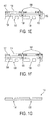
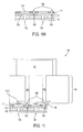
- FIGS.1A-1I illustrate an exemplary method of making an ink jet print head according to various embodiments of the present invention.
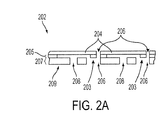
- FIGS. 2A-2H illustrate an exemplary method of making a jet stack according to various embodiments of the present teachings.
- FIG. 3 illustrates an exemplary ink jet print head according to various embodiments of the present teachings.
- the numerical values as stated for the parameter can take on negative values, In this case, the example value of range stated as "less that 10" can assume negative values, e.g. - 1, -2, -3, - 10, -20, -30, etc.
- FIGS. 1A - 1I there is an exemplary method of making an ink jet print head 100 as shown in FIGS. 1A - 1I .
- the method of making an ink jet print head 100 can include providing a partial jet stack 102 including a plurality of port holes 106 and having an ink outlet side 109 as shown in FIG. 1A .
- the partial jet stack 102 can include a brazed three layer stainless steel structure including the diaphragm 104, the body plate 105, and the inlet plate 107.
- the partial jet stack 102 can include port holes 106 formed, for example, by chemical etching.
- the method of making an ink jet print head 100 can also include providing a piezoelectric array 115 including a plurality of piezoelectric elements 114 disposed in a planarized polymer 117 as shown in FIG. 1B .
- the piezoelectric array 115 can include piezoelectric material selected from a group consisting of lead zirconate titanate (PZT), barium titanate, lead titanate, lead magnesium niobate (PMN), lead nickel niobate (PNN), and lead zinc niobate.
- the piezoelectric array 115 can include planarized polymer 117 selected from the group consisting of thermoset and thermoplastic polymers.
- the planarized polymer 117 can be selected from at least one of epoxy, polyimide, and silicone. In some embodiments, the planarized polymer 117 can have a tensile modulus less than about 2 GPa at about 120 °C. In some embodiments, the piezoelectric elements 114 and the planarized polymer 117 can have a thickness from about 10 ⁇ m to about 100 ⁇ m. In various embodiments, the step of providing a piezoelectric array 115 can further include providing the plurality of piezoelectric elements 114 disposed in an array on a carrier 112, as shown in FIG. 1B .
- the carrier 112 can be a metal support layer including one or more of a pressure sensitive adhesive and a releasable adhesive to hold the piezoelectric elements 114 to the carrier.
- the step of providing the piezoelectric array 115 can include providing a piezoelectric sheet bonded to a carrier 112, cutting or slicing the piezoelectric sheet to form a plurality of kerfed regions 216, as shown in FIG. 2B , filling the kerfed regions 216 with a polymer, and planarizing the polymer in the kerfed region to form a plurality of piezoelectric elements 114 disposed in a planarized polymer 117 as shown in FIGS. 1B and 2C .
- the step of providing the piezoelectric array 115 can include transferring one or more pre-formed piezoelectric elements 114 onto the carrier 112 and planarizing the pre-formed piezoelectric elements 114 over the carrier with a polymer 117.
- the method of making an ink jet print head 100 can further include bonding the piezoelectric array 115 to a side opposite to the ink outlet side 109 of the partial jet stack 102, wherein the partial jet stack 102 can be aligned such that the planarized polymer 117 can cover the plurality of port holes 106 as shown in FIG. 1C .
- the bonding of the piezoelectric array 115 to the partial jet stack 102 can done using an adhesive 122 including but not limited to, for example epoxy, silicone, and bismaleimide.
- the adhesive 122 can be dispensed on the partial jet stack 102. In other embodiments, the adhesive 122 can be dispensed on the piezoelectric array 115.
- a thin layer of transfer adhesive can be used.
- a bead of adhesive can be used.
- the step of bonding the piezoelectric array 115 to the partial jet stack 102 can also include thermal curing at a temperature in the range of about 100 °C to about 250 °C.
- the carrier 112 can be removed from the piezoelectric array 115 after the step of bonding the piezoelectric array 115 to the partial jet stack 102.
- the method of making an ink jet print head 100 can also include using the partial jet stack 102 as a mask to extend the port holes 106 through the planarized polymer 117 by ablating the planarized polymer 117 from the ink outlet side 109 using a laser beam 125, generated by a laser, as shown in FIG. 1 D .
- the extended port hole 166 through the planarized polymer 117 formed by laser ablation can have a uniform cross-section as shown in FIG. 1 E .
- the extended port hole 166 through the planarized polymer 117 formed by laser ablation can have a tapered cross-section as shown in FIG. 1 F .
- ablating the planarized polymer 117 from the ink outlet side 109 can include using at least one of a CO 2 laser, an excimer laser, a solid state laser, a copper vapor laser, and a fiber laser.
- a CO 2 laser can typically ablate polymers including epoxies.
- the CO 2 laser can have a low operating cost and can be ideal for high volume production.
- the CO 2 laser beam that can over-fill the mask could sequentially illuminate each port hole 106 to form the extended port holes 166 through the polymer 117 and remove an excess portion of the adhesive 122 that flows into the port hole 106 from the bonding of the piezoelectric array 115 to the partial jet stack 102, as shown in FIGS. 1 E and 1 F .
- the excimer laser can be used to flood illuminate or can be used with special optics to illuminate each of the port holes 106 to form the extended port holes 166 though the polymer 117 and remove an excess portion of the adhesive 122 from the bonding of the piezoelectric array 115 to the partial jet stack 102, as shown in FIGS. 1 E and 1 F .
- the method of making an ink jet print head 100 can further include bonding an aperture plate 130 as shown in FIG. 1G including a second plurality of outlet apertures 138 to the ink outlet side 109 of the partial jet stack 102, wherein the second plurality of outlet apertures 138 are substantially aligned with the first plurality of outlet apertures 108 as shown in FIG. 1 H .
- an adhesive such as a thermoplastic polyimide can be used in bonding the aperture plate 130 to the partial jet stack 102.
- a b-staged epoxy can used in bonding the aperture plate 130 to the partial jet stack 102.
- the aperture plate 130 can include a single layer or a two layer metal structure.
- the aperture plate 130 can be formed of stainless steel.
- the aperture plate 130 can include a polymeric plate wherein the second plurality of outlet apertures 138 can be formed by laser ablation.
- the aperture plate 130 can include polymers such as polyimide, polyetherimide, polysulfone, polyetherketone, polyphenylene sulfide, and polyester.
- the method of making an ink jet print head 100 can further include bonding filters, manifolds, other jet stack design elements to the partial jet stack 102, circuit board 140, and flexible circuit substrates.
- the method of making an ink jet print head 100 can also include cleaning the extended port holes 166 through the planarized polymer 117 and the passageway through the diaphragm 104, the body plate 105, and the inlet plate 107 prior to bonding the aperture plate 130 to the ink outlet side of the partial jet stack 102.
- the disclosed method of making an ink jet print head 100 permits cleaning of the extended port holes 166 to remove any debris formed as a result of the laser ablation of the polymer as the port holes 106, 166 are accessible from both sides, the ink outlet side 109 and the side opposite to the ink outlet side.
- each of the second plurality of outlet apertures 138 can be smaller in size compared to the first plurality of outlet apertures 108.
- each of the second plurality of outlet apertures 138 can further include nozzle for dispensing ink.
- the method of making an ink jet print head 100 can also include bonding a standoff layer 146 to the piezoelectric array 115 before the step of using the partial jet stack 102 as a mask to extend the port holes 106 through the planarized polymer 117 by ablating the planarized polymer 117 from the ink outlet side 109 using a laser beam 125, generated by a laser and extending the port holes 106 through the standoff layer 146 during the step of using the partial jet stack 102 as a mask to extend the port holes 106 through the planarized polymer 117 by ablating the planarized polymer 117 and the standoff layer 146 from the ink outlet side 109 using a laser beam 125, generated by a laser.
- the standoff layer 146 can include acrylic polymer. In other embodiments, the standoff layer 146 can include silicone. In certain embodiments, the standoff layer 146 can be precut having an adhesive portion that can be aligned and bonded with heat treatment.
- the method of making an ink jet print head 100 can further include bonding a circuit board 140 including a plurality of vias 142 and a plurality of contact pads 144 to the piezoelectric array 115 using a standoff layer 146, wherein the standoff layer 146 provides a fluid seal between the circuit board 140 and the plurality of port holes 106 and providing an ink manifold 150, wherein each of the plurality of vias 142 and each of the plurality of port holes 106 provide an individual inlet connecting the ink manifold 150 with each of the second plurality of outlet apertures 138, as shown in FIG. 1I .
- the method of making a jet stack 200 can include providing a partial jet stack 202 including a diaphragm 204, a plurality of port holes 206, a plurality of inlet channels and a first plurality of out let apertures 208, and having an ink outlet side 209, as shown in FIG. 2A .
- the method of making a jet stack 200 can also include providing a piezoelectric array 210 on a carrier 212 including a plurality of piezoelectric elements 214 and a plurality of kerfed regions 216, as shown in FIG. 2B .
- each of the kerfed regions can be wide enough to accommodate the port holes 106. In some embodiments, each of the kerfed regions can have width in the range of about 100 ⁇ m to about 400 ⁇ m.
- the method of making a jet stack 200 can further include depositing a polymer 217 in the kerfed regions 116 and planarizing the polymer 217 in the kerfed regions 216 to form a polymer planarized piezoelectric array 215, as shown in FIG. 2C .
- the kerfed regions 216 can be filled with a prepolymer liquid or paste, which can then be polymerized.
- the method of making a jet stack 200 can also include bonding the polymer planarized piezoelectric array 215 to a side opposite to the ink outlet side 209 of the partial jet stack 202 using an adhesive 222, wherein the partial jet stack 202 is aligned such that the planarized polymer 217 covers the plurality of port holes 206, as shown in FIG. 2D .
- the adhesive 222 forms a thin layer between the partial jet stack 202 and the polymer planarized piezoelectric array 215, with an excess portion of the adhesive 222 flowing into the port hole 206 from the bonding of the piezoelectric array 215 to the partial jet stack 202.
- the method of making a jet stack 200 can further include using the partial jet stack 202 as a mask to extend the port holes 206 through the polymer 217 by ablating the polymer 217 and an excess portion of the adhesive 222 from the ink outlet side 209 using a laser beam 225, generated by a laser, as shown in FIG. 2E .
- the step of ablating the planarized polymer 217 from the ink outlet side 209 can include using at least one of a CO 2 laser, an excimer laser, a solid state laser, a copper vapor laser, and a fiber laser.
- the method of making a jet stack 200 can include the providing a partial jet stack 202 including four layers or less.
- the method of making a jet stack 200 can also include cleaning the extended port holes 266 through the planarized polymer 217 to remove any debris from the ablation of the planarized polymer 217 and the adhesive, as shown in FIG. 2G and bonding an aperture plate 230 as shown in FIG. 2G including a second plurality of outlet apertures 238 to the ink outlet side 209 of the partial jet stack 202 as shown in FIG. 2H , wherein the second plurality of outlet apertures 238 can be substantially aligned with the first plurality of outlet apertures 208.
- FIG. 3 shows a schematic illustration of an exemplary ink jet print head 300.
- the ink jet print head 300 can include a partial jet stack 302 including a diaphragm 304 having an ink outlet side, a body plate 305 disposed under the ink outlet side of the diaphragm 304, and an inlet plate 307 including a plurality of inlet channels 303 and a first plurality of outlet apertures 308 disposed under the body plate 305, wherein the diaphragm 304 includes a plurality of port holes 306.
- the ink jet print head 300 can also include a piezoelectric array 315 including a plurality of piezoelectric elements 314 disposed in a planarized polymer 317 bonded to a side opposite to the ink outlet side of the diaphragm 304 such that the planarized polymer 317 covers the plurality of port holes 306.
- the ink jet print head 300 can include a laser ablated hole 366 extending each of the plurality of port holes 306 through the planarized polymer 317.
- the laser ablated hole 366 can include a tapered cross section.
- the ink jet print head 300 can further include an aperture plate 330 including a second plurality of outlet apertures 338 bonded to the inlet plate 307 of the partial jet stack 302, wherein the second plurality of outlet apertures 338 are substantially aligned with the first plurality of outlet apertures 308.
- the ink jet print head 300 can also include a circuit board 340 including a plurality of vias 342, a plurality of contact pads 344, and a plurality of electrical connections 345 bonded to the piezoelectric array 315 with a standoff layer 346, wherein the standoff layer 346 provides a fluid seal between the circuit board 340 and the plurality of port holes 306.
- the ink jet print head 300 can further include an ink manifold 350, wherein each of the plurality of vias 342 and each of the plurality of port holes 306, 366 can provide an individual inlet connecting the ink manifold 350 with each of the second plurality of outlet apertures 338.
- the printing apparatus can include a partial jet stack 102 including a diaphragm 104 having an ink outlet side 109, a body plate 105 disposed under the ink outlet side 109 of the diaphragm 104, and an inlet plate 107 including a plurality of inlet channels 103 and a first plurality of outlet apertures 108 disposed under the body plate 105, wherein the diaphragm 104 includes a plurality of port holes 106.
- the printing apparatus can also include a piezoelectric array 115 including a plurality of piezoelectric elements 114 disposed in a planarized polymer 117 bonded to a side opposite to the ink outlet side 109 of the diaphragm 104 such that the planarized polymer 117 covers the plurality of port holes 106 and an aperture plate 130 including a second plurality of outlet apertures 138 bonded to the inlet plate 107 of the partial jet stack 102, wherein the second plurality of outlet apertures 138 are substantially aligned with the first plurality of outlet apertures 108.
- the printing apparatus can further include a circuit board 140 including a plurality of vias 142 and a plurality of contact pads144 bonded to the piezoelectric array 115 with a standoff layer 146, wherein the standoff layer 146 provides a fluid seal between the circuit board 140 and the plurality of port holes 106 and an ink manifold 150, wherein each of the plurality of vias 142 and each of the plurality of port holes 106 provide an individual inlet connecting the ink manifold 150 with each of the second plurality of outlet apertures 138.
Landscapes
- Engineering & Computer Science (AREA)
- Manufacturing & Machinery (AREA)
- Physics & Mathematics (AREA)
- Optics & Photonics (AREA)
- Particle Formation And Scattering Control In Inkjet Printers (AREA)
Abstract
Description
- The subject matter of this invention relates to ink jet printing devices. More particularly, the subject matter of this invention relates to high density piezoelectric ink jet print heads and methods of making a high density piezoelectric ink jet print heads.
- Drop on demand ink jet technology is widely used in the printing industry. Drop on demand ink jet printers use either thermal or piezoelectric technology. A piezoelectric ink jet has an advantage over a thermal ink jet in that wider variety of inks can be used. It is desirable to increase the printing resolution of an ink jet printer employing piezoelectric ink jet technology. To increase the jet density of the piezoelectric ink jet print head, one can eliminate manifolds internal to the jet stack. It is further desirable to have a single port through the back of the jet stack for each jet. However, this implies that the large number of ports must pass vertically through the diaphragm and between the piezoelectric actuators for neighboring jets. To enable clean open port holes that can be sealed ink passages requires a significant different design and assembly processes than what is used currently.
- Thus, there is a need to overcome these and other problems of the prior art to provide a system and method of forming a high jet density in piezoelectric ink jet print head.
- In accordance with the invention, there is a method of making an ink jet print head. The method can include providing a partial jet stack including a plurality of port holes and having an ink outlet side and providing a piezoelectric array including a plurality of piezoelectric elements disposed in a planarized polymer. The method can further include bonding the piezoelectric array to a side opposite to the ink outlet side of the partial jet stack, wherein the partial jet stack is aligned such that the planarized polymer covers the plurality of port holes and using the partial jet stack as a mask to extend the port holes through the planarized polymer by ablating the planarized polymer from the ink outlet side using a laser beam, generated by a laser. In a further embodiment the method further comprises:
- bonding a circuit board comprising a plurality of vias and a plurality of contact pads to the piezoelectric array using a standoff layer, wherein the standoff layer provides a fluid seal between the circuit board and the plurality of port holes; and
- providing an ink manifold, wherein each of the plurality of vias and each of the plurality of port holes provide an individual inlet connecting the ink manifold with each of the second plurality of outlet apertures.
- cleaning the port holes through the planarized polymer to remove any debris from the ablation of the planarized polymer; and
- bonding an aperture plate comprising a second plurality of outlet apertures to the ink outlet side of the partial jet stack, wherein the second plurality of outlet apertures are substantially aligned with the first plurality of outlet apertures.
- According to various embodiments of the present teachings, there is a method of making a jet stack. The method can include providing a partial jet stack including a diaphragm, a plurality of port holes, a plurality of inlet channels, a first plurality of outlet apertures, and having an ink outlet side and providing a piezoelectric array on a carrier including a plurality of piezoelectric elements and a plurality of kerfed regions. The method can also include depositing a polymer in the kerfed regions, planarizing the polymer in the kerfed regions to form a polymer planarized piezoelectric array, and bonding the polymer planarized piezoelectric array to a side opposite to the ink outlet side of the partial jet stack using an adhesive, wherein the partial jet stack is aligned such that the planarized polymer covers the plurality of port holes. The method can further include using the partial jet stack as a mask to extend the port holes through the polymer by ablating the polymer and an excess portion of the adhesive from the ink outlet side using a laser beam, generated by a laser.
- According to yet another embodiment of the present teachings, there is a jet stack. The jet stack can include a partial jet stack including a diaphragm having an ink outlet side, a body plate disposed under the ink outlet side of the diaphragm, and an inlet plate including a plurality of inlet channels and a first plurality of outlet apertures disposed under the body plate, wherein the diaphragm includes a plurality of port holes. The jet stack can also include a piezoelectric array including a plurality of piezoelectric elements disposed in a planarized polymer bonded to a side opposite to the ink outlet side of the diaphragm such that the planarized polymer covers the plurality of port holes.
In a further embodiment a laser ablated hole extends each of the plurality of port holes through the planarized polymer.
In a further embodiment the laser ablated hole comprises a tapered cross section.
In a further embodiment the planarized polymer is selected from the group consisting of thermoset and thermoplastic polymers.
In a further embodiment the planarized polymers have a tensile modulus less than about 2 GPa at about 120 °C.
In a further embodiment the jet stack further comprises an aperture plate comprising a second plurality of outlet apertures bonded to the inlet plate of the partial jet stack, wherein the second plurality of outlet apertures are substantially aligned with the first plurality of outlet apertures. - According to another embodiment of the present teachings, there is an ink jet print head. The ink jet print head can include a partial jet stack including a diaphragm having an ink outlet side, a body plate disposed under the ink outlet side of the diaphragm, and an inlet plate including a plurality of inlet channels and a first plurality of outlet apertures disposed under the body plate, wherein the diaphragm includes a plurality of port holes. The ink jet print head can also include a piezoelectric array including a plurality of piezoelectric elements disposed in a planarized polymer bonded to a side opposite to the ink outlet side of the diaphragm such that the planarized polymer covers the plurality of port holes. The ink jet print head can also include an aperture plate including a second plurality of outlet apertures bonded to the inlet plate of the partial jet stack, wherein the second plurality of outlet apertures are substantially aligned with the first plurality of outlet apertures. The ink jet print head can further include a circuit board including a plurality of vias and a plurality of contact pads bonded to the piezoelectric array with a standoff layer, wherein the standoff layer provides a fluid seal between the circuit board and the plurality of port holes and an ink manifold, wherein each of the plurality of vias and each of the plurality of port holes provide an individual inlet connecting the ink manifold with each of the second plurality of outlet apertures.
- According to yet another embodiment of the present teachings, there is a printing apparatus. The printing apparatus can include a partial jet stack including a diaphragm having an ink outlet side, a body plate disposed under the ink outlet side of the diaphragm, and an inlet plate including a plurality of inlet channels and a first plurality of outlet apertures disposed under the body plate, wherein the diaphragm includes a plurality of port holes. The printing apparatus can also include a piezoelectric array including a plurality of piezoelectric elements disposed in a planarized polymer bonded to a side opposite to the ink outlet side of the diaphragm such that the planarized polymer covers the plurality of port holes. The printing apparatus can further include an aperture plate including a second plurality of outlet apertures bonded to the inlet plate of the partial jet stack, wherein the second plurality of outlet apertures are substantially aligned with the first plurality of outlet apertures. The printing apparatus can further include a circuit board including a plurality of vias and a plurality of contact pads bonded to the piezoelectric array with a standoff layer, wherein the standoff layer provides a fluid seal between the circuit board and the plurality of port holes and an ink manifold, wherein each of the plurality of vias and each of the plurality of port holes provide an individual inlet connecting the ink manifold with each of the second plurality of outlet apertures.
- Additional advantages of the embodiments will be set forth in part in the description which follows, and in part will be obvious from the description, or may be learned by practice of the invention. The advantages will be realized and attained by means of the elements and combinations particularly pointed out in the appended claims.
- It is to be understood that both the foregoing general description and the following detailed description are exemplary and explanatory only and are not restrictive of the invention, as claimed.
- The accompanying drawings, which are incorporated in and constitute a part of this specification, illustrate embodiments of the invention and together with the description, serve to explain the principles of the invention.
-
FIGS.1A-1I illustrate an exemplary method of making an ink jet print head according to various embodiments of the present invention. -
FIGS. 2A-2H illustrate an exemplary method of making a jet stack according to various embodiments of the present teachings. -
FIG. 3 illustrates an exemplary ink jet print head according to various embodiments of the present teachings. - Reference will now be made in detail to the present embodiments, examples of which are illustrated in the accompanying drawings. Wherever possible, the same reference numbers will be used throughout the drawings to refer to the same or like parts.
- Notwithstanding that the numerical ranges and parameters setting forth the broad scope of the invention are approximations, the numerical values set forth in the specific examples are reported as precisely as possible. Any numerical value, however, inherently contains certain errors necessarily resulting from the standard deviation found in their respective testing measurements. Moreover, all ranges disclosed herein are to be understood to encompass any and all sub-ranges subsumed therein. For example, a range of "less than 10" can include any and all sub-ranges between (and including) the minimum value of zero and the maximum value of 10, that is, any and all sub-ranges having a minimum value of equal to or greater than zero and a maximum value of equal to or less than 10, e.g., 1 to 5. In certain cases, the numerical values as stated for the parameter can take on negative values, In this case, the example value of range stated as "less that 10" can assume negative values, e.g. - 1, -2, -3, - 10, -20, -30, etc.
- According to various embodiments of the present teachings, there is an exemplary method of making an ink
jet print head 100 as shown inFIGS. 1A - 1I . The method of making an inkjet print head 100 can include providing apartial jet stack 102 including a plurality of port holes 106 and having anink outlet side 109 as shown inFIG. 1A . In various embodiments, thepartial jet stack 102 as shown inFIG. 1A can include adiaphragm 104, abody plate 105 disposed under thediaphragm 104, and aninlet plate 107 including a plurality ofinlet channels 103 and a first plurality ofoutlet apertures 108 disposed under thebody plate 105, wherein the plurality of port holes 106 includes a passageway through thediaphragm 104, thebody plate 105, and theinlet plate 107. In some embodiments, thepartial jet stack 102 can include a brazed three layer stainless steel structure including thediaphragm 104, thebody plate 105, and theinlet plate 107. In other embodiments, thepartial jet stack 102 can include port holes 106 formed, for example, by chemical etching. - The method of making an ink
jet print head 100 can also include providing apiezoelectric array 115 including a plurality ofpiezoelectric elements 114 disposed in aplanarized polymer 117 as shown inFIG. 1B . In some embodiments, thepiezoelectric array 115 can include piezoelectric material selected from a group consisting of lead zirconate titanate (PZT), barium titanate, lead titanate, lead magnesium niobate (PMN), lead nickel niobate (PNN), and lead zinc niobate. In various embodiments, thepiezoelectric array 115 can includeplanarized polymer 117 selected from the group consisting of thermoset and thermoplastic polymers. In other embodiments, theplanarized polymer 117 can be selected from at least one of epoxy, polyimide, and silicone. In some embodiments, theplanarized polymer 117 can have a tensile modulus less than about 2 GPa at about 120 °C. In some embodiments, thepiezoelectric elements 114 and theplanarized polymer 117 can have a thickness from about 10 µm to about 100 µm. In various embodiments, the step of providing apiezoelectric array 115 can further include providing the plurality ofpiezoelectric elements 114 disposed in an array on acarrier 112, as shown inFIG. 1B . Thecarrier 112 can be a metal support layer including one or more of a pressure sensitive adhesive and a releasable adhesive to hold thepiezoelectric elements 114 to the carrier. In various embodiments, the step of providing thepiezoelectric array 115 can include providing a piezoelectric sheet bonded to acarrier 112, cutting or slicing the piezoelectric sheet to form a plurality ofkerfed regions 216, as shown inFIG. 2B , filling thekerfed regions 216 with a polymer, and planarizing the polymer in the kerfed region to form a plurality ofpiezoelectric elements 114 disposed in aplanarized polymer 117 as shown inFIGS. 1B and2C . In some embodiments, the step of providing thepiezoelectric array 115 can include transferring one or more pre-formedpiezoelectric elements 114 onto thecarrier 112 and planarizing the pre-formedpiezoelectric elements 114 over the carrier with apolymer 117. - The method of making an ink
jet print head 100 can further include bonding thepiezoelectric array 115 to a side opposite to theink outlet side 109 of thepartial jet stack 102, wherein thepartial jet stack 102 can be aligned such that theplanarized polymer 117 can cover the plurality of port holes 106 as shown inFIG. 1C . In various embodiments, the bonding of thepiezoelectric array 115 to thepartial jet stack 102 can done using an adhesive 122 including but not limited to, for example epoxy, silicone, and bismaleimide. In some embodiments, the adhesive 122 can be dispensed on thepartial jet stack 102. In other embodiments, the adhesive 122 can be dispensed on thepiezoelectric array 115. In some other embodiments, a thin layer of transfer adhesive can be used. Yet in other embodiments, a bead of adhesive can be used. The step of bonding thepiezoelectric array 115 to thepartial jet stack 102 can also include thermal curing at a temperature in the range of about 100 °C to about 250 °C. In some embodiments, thecarrier 112 can be removed from thepiezoelectric array 115 after the step of bonding thepiezoelectric array 115 to thepartial jet stack 102. - The method of making an ink
jet print head 100 can also include using thepartial jet stack 102 as a mask to extend the port holes 106 through theplanarized polymer 117 by ablating theplanarized polymer 117 from theink outlet side 109 using alaser beam 125, generated by a laser, as shown inFIG. 1 D . In some embodiments, the extendedport hole 166 through theplanarized polymer 117 formed by laser ablation can have a uniform cross-section as shown inFIG. 1 E . In other embodiments, the extendedport hole 166 through theplanarized polymer 117 formed by laser ablation can have a tapered cross-section as shown inFIG. 1 F . - Several parameters for laser ablation such as wavelength of the laser, laser pulse duration, repetition rate, laser power depends on a number of factors including polymer's optical properties and thickness of the polymer to be ablated. However, one of ordinary skill in the art can determine them. In various embodiments, ablating the
planarized polymer 117 from theink outlet side 109 can include using at least one of a CO2 laser, an excimer laser, a solid state laser, a copper vapor laser, and a fiber laser. One of ordinary skill in the art would know that the CO2 laser and the excimer laser can typically ablate polymers including epoxies. The CO2 laser can have a low operating cost and can be ideal for high volume production. The CO2 laser beam that can over-fill the mask could sequentially illuminate eachport hole 106 to form the extended port holes 166 through thepolymer 117 and remove an excess portion of the adhesive 122 that flows into theport hole 106 from the bonding of thepiezoelectric array 115 to thepartial jet stack 102, as shown inFIGS. 1 E and 1 F . Furthermore, one of ordinary skill in the art would also know that the excimer laser can be used to flood illuminate or can be used with special optics to illuminate each of the port holes 106 to form the extended port holes 166 though thepolymer 117 and remove an excess portion of the adhesive 122 from the bonding of thepiezoelectric array 115 to thepartial jet stack 102, as shown inFIGS. 1 E and 1 F . - The method of making an ink
jet print head 100 can further include bonding anaperture plate 130 as shown inFIG. 1G including a second plurality ofoutlet apertures 138 to theink outlet side 109 of thepartial jet stack 102, wherein the second plurality ofoutlet apertures 138 are substantially aligned with the first plurality ofoutlet apertures 108 as shown inFIG. 1 H . In various embodiments, an adhesive such as a thermoplastic polyimide can be used in bonding theaperture plate 130 to thepartial jet stack 102. In some embodiments, a b-staged epoxy can used in bonding theaperture plate 130 to thepartial jet stack 102. In some other embodiments, theaperture plate 130 can include a single layer or a two layer metal structure. Yet, in other embodiments, theaperture plate 130 can be formed of stainless steel. In various embodiments, theaperture plate 130 can include a polymeric plate wherein the second plurality ofoutlet apertures 138 can be formed by laser ablation. In some embodiments, theaperture plate 130 can include polymers such as polyimide, polyetherimide, polysulfone, polyetherketone, polyphenylene sulfide, and polyester. In various embodiments, the method of making an inkjet print head 100 can further include bonding filters, manifolds, other jet stack design elements to thepartial jet stack 102,circuit board 140, and flexible circuit substrates. In some embodiments, the method of making an inkjet print head 100 can also include cleaning the extended port holes 166 through theplanarized polymer 117 and the passageway through thediaphragm 104, thebody plate 105, and theinlet plate 107 prior to bonding theaperture plate 130 to the ink outlet side of thepartial jet stack 102. The disclosed method of making an inkjet print head 100 permits cleaning of the extended port holes 166 to remove any debris formed as a result of the laser ablation of the polymer as the port holes 106, 166 are accessible from both sides, theink outlet side 109 and the side opposite to the ink outlet side. In various embodiments, each of the second plurality ofoutlet apertures 138 can be smaller in size compared to the first plurality ofoutlet apertures 108. In other embodiments, each of the second plurality ofoutlet apertures 138 can further include nozzle for dispensing ink. - In various embodiments, the method of making an ink
jet print head 100 can also include bonding astandoff layer 146 to thepiezoelectric array 115 before the step of using thepartial jet stack 102 as a mask to extend the port holes 106 through theplanarized polymer 117 by ablating theplanarized polymer 117 from theink outlet side 109 using alaser beam 125, generated by a laser and extending the port holes 106 through thestandoff layer 146 during the step of using thepartial jet stack 102 as a mask to extend the port holes 106 through theplanarized polymer 117 by ablating theplanarized polymer 117 and thestandoff layer 146 from theink outlet side 109 using alaser beam 125, generated by a laser. In some embodiments, thestandoff layer 146 can include acrylic polymer. In other embodiments, thestandoff layer 146 can include silicone. In certain embodiments, thestandoff layer 146 can be precut having an adhesive portion that can be aligned and bonded with heat treatment. In some embodiments, the method of making an inkjet print head 100 can further include bonding acircuit board 140 including a plurality ofvias 142 and a plurality ofcontact pads 144 to thepiezoelectric array 115 using astandoff layer 146, wherein thestandoff layer 146 provides a fluid seal between thecircuit board 140 and the plurality of port holes 106 and providing anink manifold 150, wherein each of the plurality ofvias 142 and each of the plurality of port holes 106 provide an individual inlet connecting theink manifold 150 with each of the second plurality ofoutlet apertures 138, as shown inFIG. 1I . - According to various embodiments, there is a method of making a jet stack 200 as shown in
FIGS. 2A-2H . The method of making a jet stack 200 can include providing apartial jet stack 202 including adiaphragm 204, a plurality of port holes 206, a plurality of inlet channels and a first plurality of out letapertures 208, and having anink outlet side 209, as shown inFIG. 2A . The method of making a jet stack 200 can also include providing apiezoelectric array 210 on acarrier 212 including a plurality ofpiezoelectric elements 214 and a plurality ofkerfed regions 216, as shown inFIG. 2B . In various embodiments, each of the kerfed regions can be wide enough to accommodate the port holes 106. In some embodiments, each of the kerfed regions can have width in the range of about 100 µm to about 400 µm. The method of making a jet stack 200 can further include depositing apolymer 217 in the kerfed regions 116 and planarizing thepolymer 217 in thekerfed regions 216 to form a polymer planarizedpiezoelectric array 215, as shown inFIG. 2C . In some embodiments, thekerfed regions 216 can be filled with a prepolymer liquid or paste, which can then be polymerized. The method of making a jet stack 200 can also include bonding the polymer planarizedpiezoelectric array 215 to a side opposite to theink outlet side 209 of thepartial jet stack 202 using an adhesive 222, wherein thepartial jet stack 202 is aligned such that theplanarized polymer 217 covers the plurality of port holes 206, as shown inFIG. 2D . In some embodiments, the adhesive 222 forms a thin layer between thepartial jet stack 202 and the polymer planarizedpiezoelectric array 215, with an excess portion of the adhesive 222 flowing into theport hole 206 from the bonding of thepiezoelectric array 215 to thepartial jet stack 202. The method of making a jet stack 200 can further include using thepartial jet stack 202 as a mask to extend the port holes 206 through thepolymer 217 by ablating thepolymer 217 and an excess portion of the adhesive 222 from theink outlet side 209 using alaser beam 225, generated by a laser, as shown inFIG. 2E . In some embodiments, the step of ablating theplanarized polymer 217 from theink outlet side 209 can include using at least one of a CO2 laser, an excimer laser, a solid state laser, a copper vapor laser, and a fiber laser. In various embodiments, the method of making a jet stack 200 can include the providing apartial jet stack 202 including four layers or less. The method of making a jet stack 200 can also include cleaning the extended port holes 266 through theplanarized polymer 217 to remove any debris from the ablation of theplanarized polymer 217 and the adhesive, as shown inFIG. 2G and bonding anaperture plate 230 as shown inFIG. 2G including a second plurality ofoutlet apertures 238 to theink outlet side 209 of thepartial jet stack 202 as shown inFIG. 2H , wherein the second plurality ofoutlet apertures 238 can be substantially aligned with the first plurality ofoutlet apertures 208. -
FIG. 3 shows a schematic illustration of an exemplary inkjet print head 300. The inkjet print head 300 can include apartial jet stack 302 including adiaphragm 304 having an ink outlet side, abody plate 305 disposed under the ink outlet side of thediaphragm 304, and aninlet plate 307 including a plurality ofinlet channels 303 and a first plurality ofoutlet apertures 308 disposed under thebody plate 305, wherein thediaphragm 304 includes a plurality of port holes 306. The inkjet print head 300 can also include a piezoelectric array 315 including a plurality ofpiezoelectric elements 314 disposed in aplanarized polymer 317 bonded to a side opposite to the ink outlet side of thediaphragm 304 such that theplanarized polymer 317 covers the plurality of port holes 306. In some embodiments, the inkjet print head 300 can include a laser ablatedhole 366 extending each of the plurality of port holes 306 through theplanarized polymer 317. In some other embodiments, the laser ablatedhole 366 can include a tapered cross section. In various embodiments, the inkjet print head 300 can further include an aperture plate 330 including a second plurality of outlet apertures 338 bonded to theinlet plate 307 of thepartial jet stack 302, wherein the second plurality of outlet apertures 338 are substantially aligned with the first plurality ofoutlet apertures 308. The inkjet print head 300 can also include acircuit board 340 including a plurality ofvias 342, a plurality ofcontact pads 344, and a plurality ofelectrical connections 345 bonded to the piezoelectric array 315 with astandoff layer 346, wherein thestandoff layer 346 provides a fluid seal between thecircuit board 340 and the plurality of port holes 306. The inkjet print head 300 can further include anink manifold 350, wherein each of the plurality ofvias 342 and each of the plurality of port holes 306, 366 can provide an individual inlet connecting theink manifold 350 with each of the second plurality of outlet apertures 338. - According to various embodiments, there is a printing apparatus (not shown). The printing apparatus can include a
partial jet stack 102 including adiaphragm 104 having anink outlet side 109, abody plate 105 disposed under theink outlet side 109 of thediaphragm 104, and aninlet plate 107 including a plurality ofinlet channels 103 and a first plurality ofoutlet apertures 108 disposed under thebody plate 105, wherein thediaphragm 104 includes a plurality of port holes 106. The printing apparatus can also include apiezoelectric array 115 including a plurality ofpiezoelectric elements 114 disposed in aplanarized polymer 117 bonded to a side opposite to theink outlet side 109 of thediaphragm 104 such that theplanarized polymer 117 covers the plurality of port holes 106 and anaperture plate 130 including a second plurality ofoutlet apertures 138 bonded to theinlet plate 107 of thepartial jet stack 102, wherein the second plurality ofoutlet apertures 138 are substantially aligned with the first plurality ofoutlet apertures 108. The printing apparatus can further include acircuit board 140 including a plurality ofvias 142 and a plurality of contact pads144 bonded to thepiezoelectric array 115 with astandoff layer 146, wherein thestandoff layer 146 provides a fluid seal between thecircuit board 140 and the plurality of port holes 106 and anink manifold 150, wherein each of the plurality ofvias 142 and each of the plurality of port holes 106 provide an individual inlet connecting theink manifold 150 with each of the second plurality ofoutlet apertures 138. - While the invention has been illustrated with respect to one or more implementations, alterations and/or modifications can be made to the illustrated examples without departing from the spirit and scope of the appended claims. In addition, while a particular feature of the invention may have been disclosed with respect to only one of several implementations, such feature may be combined with one or more other features of the other implementations as may be desired and advantageous for any given or particular function. Furthermore, to the extent that the terms "including", "includes", "having", "has", "with", or variants thereof are used in either the detailed description and the claims, such terms are intended to be inclusive in a manner similar to the term "comprising."
In a further embodiment the method further comprises bonding one or more of filters, manifolds, circuit board, and flexible circuit substrates.
In a further embodiment the method further comprises providing a partial jet stack comprising four layers or less.
In a further embodiment the method further comprises:
Claims (10)
- A method of making an ink jet print head comprising:providing a partial jet stack comprising a plurality of port holes and having an ink outlet side;providing a piezoelectric array comprising a plurality of piezoelectric elements disposed in a planarized polymer;bonding the piezoelectric array to a side opposite to the ink outlet side of the partial jet stack, wherein the partial jet stack is aligned such that the planarized polymer covers the plurality of port holes; andusing the partial jet stack as a mask to extend the port holes through the planarized polymer by ablating the planarized polymer from the ink outlet side using a laser beam, generated by a laser.
- The method of claim 1 wherein the partial jet stack comprises:a diaphragm;a body plate disposed under the diaphragm; andan inlet plate comprising a plurality of inlet channels and a first plurality of outlet apertures disposed under the body plate,wherein the plurality of port holes comprises a passageway through the diaphragm, the body plate, and the inlet plate.
- The method of claim 1 further comprising bonding an aperture plate comprising a second plurality of outlet apertures to the ink outlet side of the partial jet stack, wherein the second plurality of outlet apertures are substantially aligned with the first plurality of outlet apertures.
- The method of claim 1, wherein the step of providing a piezoelectric array comprises providing the plurality of piezoelectric elements disposed in an array on a carrier.
- The method of claim 3 further comprising cleaning the passageway prior to bonding the aperture plate to the inlet plate.
- The method of claim 1 further comprising:bonding a standoff layer to the piezoelectric array before the step of using the partial jet stack as a mask to extend the port holes through the planarized polymer by ablating the planarized polymer from the ink outlet side using a laser beam, generated by a laser; andextending the port holes through the standoff layer during the step of using the partial jet stack as a mask to extend the port holes through the planarized polymer by ablating the planarized polymer and the standoff layer from the ink outlet side using the laser beam, generated by the laser.
- A method of making a jet stack comprising:providing a partial jet stack comprising a diaphragm, a plurality of port holes, a plurality of inlet channels, a first plurality of outlet apertures, and having an ink outlet side;providing a piezoelectric array on a carrier comprising a plurality of piezoelectric elements and a plurality of kerfed regions;depositing a polymer in the kerfed regions;planarizing the polymer in the kerfed regions to form a polymer planarized piezoelectric array;bonding the polymer planarized piezoelectric array to a side opposite to the ink outlet side of the partial jet stack using an adhesive, wherein the partial jet stack is aligned such that the planarized polymer covers the plurality of port holes; andusing the partial jet stack as a mask to extend the port holes through the polymer by ablating the polymer and an excess portion of the adhesive from the ink outlet side using a laser beam, generated by a laser.
- A jet stack comprising:a partial jet stack comprising a diaphragm having an ink outlet side, a body plate disposed under the ink outlet side of the diaphragm, and an inlet plate comprising a plurality of inlet channels and a first plurality of outlet apertures disposed under the body plate, wherein the diaphragm comprises a plurality of port holes; anda piezoelectric array comprising a plurality of piezoelectric elements disposed in a planarized polymer bonded to a side opposite to the ink outlet side of the diaphragm such that the planarized polymer covers the plurality of port holes.
- An ink jet print head comprising:a partial jet stack comprising a diaphragm having an ink outlet side, a body plate disposed under the ink outlet side of the diaphragm, and an inlet plate comprising a plurality of inlet channels and a first plurality of outlet apertures disposed under the body plate, wherein the diaphragm comprises a plurality of port holes;a piezoelectric array comprising a plurality of piezoelectric elements disposed in a planarized polymer bonded to a side opposite to the ink outlet side of the diaphragm such that the planarized polymer covers the plurality of port holes;an aperture plate comprising a second plurality of outlet apertures bonded to the inlet plate of the partial jet stack, wherein the second plurality of outlet apertures are substantially aligned with the first plurality of outlet apertures;a circuit board comprising a plurality of vias and a plurality of contact pads bonded to the piezoelectric array with a standoff layer, wherein the standoff layer provides a fluid seal between the circuit board and the plurality of port holes; andan ink manifold, wherein each of the plurality of vias and each of the plurality of port holes provide an individual inlet connecting the ink manifold with each of the second plurality of outlet apertures.
- A printing apparatus comprising:a partial jet stack comprising a diaphragm having an ink outlet side, a body plate disposed under the ink outlet side of the diaphragm, and an inlet plate comprising a plurality of inlet channels and a first plurality of outlet apertures disposed under the body plate, wherein the diaphragm comprises a plurality of port holes;a piezoelectric array comprising a plurality of piezoelectric elements disposed in a planarized polymer bonded to a side opposite to the ink outlet side of the diaphragm such that the planarized polymer covers the plurality of port holes;an aperture plate comprising a second plurality of outlet apertures bonded to the inlet plate of the partial jet stack, wherein the second plurality of outlet apertures are substantially aligned with the first plurality of outlet apertures;a circuit board comprising a plurality of vias and a plurality of contact pads bonded to the piezoelectric array with a standoff layer, wherein the standoff layer provides a fluid seal between the circuit board and the plurality of port holes; andan ink manifold, wherein each of the plurality of vias and each of the plurality of port holes provide an individual inlet connecting the ink manifold with each of the second plurality of outlet apertures.
Applications Claiming Priority (1)
| Application Number | Priority Date | Filing Date | Title |
|---|---|---|---|
| US11/692,616 US7959266B2 (en) | 2007-03-28 | 2007-03-28 | Self aligned port hole opening process for ink jet print heads |
Publications (2)
| Publication Number | Publication Date |
|---|---|
| EP1974921A1 true EP1974921A1 (en) | 2008-10-01 |
| EP1974921B1 EP1974921B1 (en) | 2014-01-22 |
Family
ID=39484546
Family Applications (1)
| Application Number | Title | Priority Date | Filing Date |
|---|---|---|---|
| EP08151999.3A Ceased EP1974921B1 (en) | 2007-03-28 | 2008-02-27 | Self Aligned Port Hole Opening Process for Ink Jet Print Heads |
Country Status (7)
| Country | Link |
|---|---|
| US (1) | US7959266B2 (en) |
| EP (1) | EP1974921B1 (en) |
| JP (1) | JP4981725B2 (en) |
| KR (1) | KR101440784B1 (en) |
| CN (2) | CN102407669B (en) |
| BR (1) | BRPI0800929A2 (en) |
| MX (1) | MX2008003916A (en) |
Cited By (1)
| Publication number | Priority date | Publication date | Assignee | Title |
|---|---|---|---|---|
| EP2366548A1 (en) * | 2010-03-19 | 2011-09-21 | Fujifilm Corporation | Bonded circuits and seals in a printing device |
Families Citing this family (22)
| Publication number | Priority date | Publication date | Assignee | Title |
|---|---|---|---|---|
| US7448734B2 (en) * | 2004-01-21 | 2008-11-11 | Silverbrook Research Pty Ltd | Inkjet printer cartridge with pagewidth printhead |
| US8360557B2 (en) * | 2008-12-05 | 2013-01-29 | Xerox Corporation | Method for laser drilling fluid ports in multiple layers |
| US8240818B2 (en) * | 2009-12-17 | 2012-08-14 | Xerox Corporation | Inkjet ejector having a polymer aperture plate attached to an outlet plate and method for assembling an inkjet ejector |
| JP5943590B2 (en) * | 2011-01-07 | 2016-07-05 | 日本発條株式会社 | Piezoelectric element manufacturing method, piezoelectric element, piezoelectric actuator, and head suspension |
| US8465659B2 (en) | 2011-01-21 | 2013-06-18 | Xerox Corporation | Polymer layer removal on pzt arrays using a plasma etch |
| US8585183B2 (en) * | 2011-03-22 | 2013-11-19 | Xerox Corporation | High density multilayer interconnect for print head |
| US8550601B2 (en) * | 2011-03-23 | 2013-10-08 | Xerox Corporation | Use of photoresist material as an interstitial fill for PZT printhead fabrication |
| US8567924B2 (en) * | 2011-04-07 | 2013-10-29 | Xerox Corporation | Patterned conductive array and self leveling epoxy |
| US8585187B2 (en) * | 2011-04-29 | 2013-11-19 | Xerox Corporation | High density electrical interconnect for printing devices using flex circuits and dielectric underfill |
| US9355834B2 (en) | 2011-07-28 | 2016-05-31 | Hewlett-Packard Development Company, L.P. | Adhesive transfer |
| US8585185B2 (en) * | 2011-09-22 | 2013-11-19 | Xerox Corporation | High density electrical interconnect using limited density flex circuits |
| US8794743B2 (en) * | 2011-11-30 | 2014-08-05 | Xerox Corporation | Multi-film adhesive design for interfacial bonding printhead structures |
| US8814328B2 (en) * | 2011-12-13 | 2014-08-26 | Xerox Corporation | Polymer film as an interstitial fill for PZT printhead fabrication |
| US8980026B2 (en) * | 2012-09-28 | 2015-03-17 | Apple Inc. | Gap seals for electronic device structures |
| US8740357B1 (en) | 2013-02-05 | 2014-06-03 | Xerox Corporation | Method and structure for sealing fine fluid features in a printing device |
| KR101827070B1 (en) | 2013-02-28 | 2018-02-07 | 휴렛-팩커드 디벨롭먼트 컴퍼니, 엘.피. | Molding a fluid flow structure |
| US10821729B2 (en) | 2013-02-28 | 2020-11-03 | Hewlett-Packard Development Company, L.P. | Transfer molded fluid flow structure |
| EP3296113B1 (en) | 2013-02-28 | 2019-08-28 | Hewlett-Packard Development Company, L.P. | Molded print bar |
| US9724920B2 (en) | 2013-03-20 | 2017-08-08 | Hewlett-Packard Development Company, L.P. | Molded die slivers with exposed front and back surfaces |
| TWI572494B (en) * | 2013-07-29 | 2017-03-01 | 惠普發展公司有限責任合夥企業 | Fluid flow structure and method of manufacturing fluid passage in fluid flow structure |
| US10549386B2 (en) * | 2016-02-29 | 2020-02-04 | Xerox Corporation | Method for ablating openings in unsupported layers |
| CN120816165A (en) * | 2025-07-28 | 2025-10-21 | 珠海晶瓷电子科技有限公司 | Ceramic substrate drilling method |
Citations (6)
| Publication number | Priority date | Publication date | Assignee | Title |
|---|---|---|---|---|
| JP2001088303A (en) * | 1992-03-18 | 2001-04-03 | Seiko Epson Corp | Ink jet print head and method of manufacturing the same |
| US20020149652A1 (en) | 1999-12-10 | 2002-10-17 | Fujitsu Limited | Ink jet head and printing apparatus |
| US20030058310A1 (en) * | 2001-08-28 | 2003-03-27 | Seiko Epson Corporation | Liquid-jet head, fabricating method of the same, and liquid-jet apparatus |
| US20040104977A1 (en) * | 2001-05-28 | 2004-06-03 | Fuji Xerox Co., Ltd. | Inkjet recording head and method for manufacturing the same |
| US20060066693A1 (en) * | 2000-03-31 | 2006-03-30 | Fuji Photo Film Co., Ltd. | Multi-nozzle ink jet head |
| US20060209139A1 (en) * | 2005-03-15 | 2006-09-21 | Fuji Xerox Co., Ltd. | Electrical connection substrate, droplet discharge head, and droplet discharge apparatus |
Family Cites Families (6)
| Publication number | Priority date | Publication date | Assignee | Title |
|---|---|---|---|---|
| JP2001096746A (en) * | 1999-10-01 | 2001-04-10 | Ricoh Co Ltd | Ink jet recording head and method of manufacturing the same |
| JP2001191540A (en) * | 2000-01-06 | 2001-07-17 | Ricoh Co Ltd | Nozzle forming member and manufacturing method thereof, ink jet head and ink jet recording apparatus |
| JP2006044222A (en) * | 2004-06-11 | 2006-02-16 | Fuji Xerox Co Ltd | Inkjet recording head and inkjet recorder |
| JP2006044225A (en) * | 2004-06-29 | 2006-02-16 | Fuji Xerox Co Ltd | Liquid droplet ejecting head and liquid droplet ejecting apparatus |
| US7549223B2 (en) * | 2004-09-28 | 2009-06-23 | Fujifilm Corporation | Method for manufacturing a liquid ejection head |
| JP2006326868A (en) * | 2005-05-23 | 2006-12-07 | Brother Ind Ltd | Plate member structure and manufacturing method thereof |
-
2007
- 2007-03-28 US US11/692,616 patent/US7959266B2/en active Active
-
2008
- 2008-02-27 EP EP08151999.3A patent/EP1974921B1/en not_active Ceased
- 2008-03-21 JP JP2008072730A patent/JP4981725B2/en not_active Expired - Fee Related
- 2008-03-24 MX MX2008003916A patent/MX2008003916A/en active IP Right Grant
- 2008-03-27 CN CN201110239761.9A patent/CN102407669B/en not_active Expired - Fee Related
- 2008-03-27 CN CN200810087419XA patent/CN101274523B/en not_active Expired - Fee Related
- 2008-03-28 KR KR1020080028750A patent/KR101440784B1/en not_active Expired - Fee Related
- 2008-03-28 BR BRPI0800929-5A patent/BRPI0800929A2/en not_active IP Right Cessation
Patent Citations (6)
| Publication number | Priority date | Publication date | Assignee | Title |
|---|---|---|---|---|
| JP2001088303A (en) * | 1992-03-18 | 2001-04-03 | Seiko Epson Corp | Ink jet print head and method of manufacturing the same |
| US20020149652A1 (en) | 1999-12-10 | 2002-10-17 | Fujitsu Limited | Ink jet head and printing apparatus |
| US20060066693A1 (en) * | 2000-03-31 | 2006-03-30 | Fuji Photo Film Co., Ltd. | Multi-nozzle ink jet head |
| US20040104977A1 (en) * | 2001-05-28 | 2004-06-03 | Fuji Xerox Co., Ltd. | Inkjet recording head and method for manufacturing the same |
| US20030058310A1 (en) * | 2001-08-28 | 2003-03-27 | Seiko Epson Corporation | Liquid-jet head, fabricating method of the same, and liquid-jet apparatus |
| US20060209139A1 (en) * | 2005-03-15 | 2006-09-21 | Fuji Xerox Co., Ltd. | Electrical connection substrate, droplet discharge head, and droplet discharge apparatus |
Cited By (1)
| Publication number | Priority date | Publication date | Assignee | Title |
|---|---|---|---|---|
| EP2366548A1 (en) * | 2010-03-19 | 2011-09-21 | Fujifilm Corporation | Bonded circuits and seals in a printing device |
Also Published As
| Publication number | Publication date |
|---|---|
| CN101274523B (en) | 2012-02-22 |
| US20080239022A1 (en) | 2008-10-02 |
| BRPI0800929A2 (en) | 2008-11-11 |
| CN101274523A (en) | 2008-10-01 |
| KR101440784B1 (en) | 2014-09-17 |
| US7959266B2 (en) | 2011-06-14 |
| KR20080088485A (en) | 2008-10-02 |
| CN102407669B (en) | 2015-04-15 |
| MX2008003916A (en) | 2009-02-27 |
| JP2008238820A (en) | 2008-10-09 |
| JP4981725B2 (en) | 2012-07-25 |
| EP1974921B1 (en) | 2014-01-22 |
| CN102407669A (en) | 2012-04-11 |
Similar Documents
| Publication | Publication Date | Title |
|---|---|---|
| US7959266B2 (en) | Self aligned port hole opening process for ink jet print heads | |
| EP0901906B1 (en) | Ink jet printhead with improved, laser-ablated filter | |
| KR101363562B1 (en) | Droplet deposition apparatus | |
| EP0738599B1 (en) | Ink Jet recording head and method of producing same | |
| EP0600743A2 (en) | Actuator having ceramic substrate and ink jet print head using the actuator | |
| US8585187B2 (en) | High density electrical interconnect for printing devices using flex circuits and dielectric underfill | |
| JP2009233927A (en) | Manufacturing method for inkjet head | |
| US7976133B2 (en) | Liquid-jetting apparatus and method for producing the same | |
| WO2011155129A1 (en) | Liquid discharge head and method for manufacturing liquid discharge head | |
| US7934815B2 (en) | External fluid manifold with polymer compliant wall | |
| EP1273447B1 (en) | Ink jet print head acoustic filters | |
| US8465659B2 (en) | Polymer layer removal on pzt arrays using a plasma etch | |
| JP6130308B2 (en) | How to make an inkjet printhead | |
| JP4807490B2 (en) | Inkjet head manufacturing method and inkjet head | |
| US8205969B2 (en) | Jet stack with precision port holes for ink jet printer and associated method | |
| JP7193334B2 (en) | HEAD CHIP, LIQUID JET HEAD, LIQUID JET RECORDING APPARATUS, AND HEAD CHIP MANUFACTURING METHOD | |
| JP5396367B2 (en) | Inkjet head manufacturing method | |
| JPH08118655A (en) | Inkjet nozzle plate | |
| HK1147079A (en) | Flexible circuit | |
| HK1147229B (en) | A print head and a method of aligning laminates | |
| HK1147229A1 (en) | A print head and a method of aligning laminates |
Legal Events
| Date | Code | Title | Description |
|---|---|---|---|
| PUAI | Public reference made under article 153(3) epc to a published international application that has entered the european phase |
Free format text: ORIGINAL CODE: 0009012 |
|
| AK | Designated contracting states |
Kind code of ref document: A1 Designated state(s): AT BE BG CH CY CZ DE DK EE ES FI FR GB GR HR HU IE IS IT LI LT LU LV MC MT NL NO PL PT RO SE SI SK TR |
|
| AX | Request for extension of the european patent |
Extension state: AL BA MK RS |
|
| 17P | Request for examination filed |
Effective date: 20090401 |
|
| 17Q | First examination report despatched |
Effective date: 20090508 |
|
| AKX | Designation fees paid |
Designated state(s): DE FR GB |
|
| GRAP | Despatch of communication of intention to grant a patent |
Free format text: ORIGINAL CODE: EPIDOSNIGR1 |
|
| INTG | Intention to grant announced |
Effective date: 20131001 |
|
| GRAS | Grant fee paid |
Free format text: ORIGINAL CODE: EPIDOSNIGR3 |
|
| GRAA | (expected) grant |
Free format text: ORIGINAL CODE: 0009210 |
|
| AK | Designated contracting states |
Kind code of ref document: B1 Designated state(s): DE FR GB |
|
| REG | Reference to a national code |
Ref country code: GB Ref legal event code: FG4D |
|
| REG | Reference to a national code |
Ref country code: DE Ref legal event code: R096 Ref document number: 602008030043 Country of ref document: DE Effective date: 20140306 |
|
| REG | Reference to a national code |
Ref country code: DE Ref legal event code: R097 Ref document number: 602008030043 Country of ref document: DE |
|
| PLBE | No opposition filed within time limit |
Free format text: ORIGINAL CODE: 0009261 |
|
| STAA | Information on the status of an ep patent application or granted ep patent |
Free format text: STATUS: NO OPPOSITION FILED WITHIN TIME LIMIT |
|
| 26N | No opposition filed |
Effective date: 20141023 |
|
| REG | Reference to a national code |
Ref country code: DE Ref legal event code: R097 Ref document number: 602008030043 Country of ref document: DE Effective date: 20141023 |
|
| REG | Reference to a national code |
Ref country code: FR Ref legal event code: PLFP Year of fee payment: 9 |
|
| REG | Reference to a national code |
Ref country code: FR Ref legal event code: PLFP Year of fee payment: 10 |
|
| REG | Reference to a national code |
Ref country code: FR Ref legal event code: PLFP Year of fee payment: 11 |
|
| PGFP | Annual fee paid to national office [announced via postgrant information from national office to epo] |
Ref country code: GB Payment date: 20200123 Year of fee payment: 13 |
|
| PGFP | Annual fee paid to national office [announced via postgrant information from national office to epo] |
Ref country code: FR Payment date: 20200122 Year of fee payment: 13 |
|
| GBPC | Gb: european patent ceased through non-payment of renewal fee |
Effective date: 20210227 |
|
| PG25 | Lapsed in a contracting state [announced via postgrant information from national office to epo] |
Ref country code: GB Free format text: LAPSE BECAUSE OF NON-PAYMENT OF DUE FEES Effective date: 20210227 Ref country code: FR Free format text: LAPSE BECAUSE OF NON-PAYMENT OF DUE FEES Effective date: 20210228 |
|
| PGFP | Annual fee paid to national office [announced via postgrant information from national office to epo] |
Ref country code: DE Payment date: 20230119 Year of fee payment: 16 |
|
| REG | Reference to a national code |
Ref country code: DE Ref legal event code: R119 Ref document number: 602008030043 Country of ref document: DE |
|
| PG25 | Lapsed in a contracting state [announced via postgrant information from national office to epo] |
Ref country code: DE Free format text: LAPSE BECAUSE OF NON-PAYMENT OF DUE FEES Effective date: 20240903 |
|
| PG25 | Lapsed in a contracting state [announced via postgrant information from national office to epo] |
Ref country code: DE Free format text: LAPSE BECAUSE OF NON-PAYMENT OF DUE FEES Effective date: 20240903 |