EP1973201B1 - Circuit board connector for two parallel circuit boards - Google Patents
Circuit board connector for two parallel circuit boards Download PDFInfo
- Publication number
- EP1973201B1 EP1973201B1 EP08001989A EP08001989A EP1973201B1 EP 1973201 B1 EP1973201 B1 EP 1973201B1 EP 08001989 A EP08001989 A EP 08001989A EP 08001989 A EP08001989 A EP 08001989A EP 1973201 B1 EP1973201 B1 EP 1973201B1
- Authority
- EP
- European Patent Office
- Prior art keywords
- circuit board
- base body
- contact
- board plug
- plug connection
- Prior art date
- Legal status (The legal status is an assumption and is not a legal conclusion. Google has not performed a legal analysis and makes no representation as to the accuracy of the status listed.)
- Active
Links
Images


Classifications
-
- H—ELECTRICITY
- H01—ELECTRIC ELEMENTS
- H01R—ELECTRICALLY-CONDUCTIVE CONNECTIONS; STRUCTURAL ASSOCIATIONS OF A PLURALITY OF MUTUALLY-INSULATED ELECTRICAL CONNECTING ELEMENTS; COUPLING DEVICES; CURRENT COLLECTORS
- H01R24/00—Two-part coupling devices, or either of their cooperating parts, characterised by their overall structure
- H01R24/84—Hermaphroditic coupling devices
-
- H—ELECTRICITY
- H01—ELECTRIC ELEMENTS
- H01R—ELECTRICALLY-CONDUCTIVE CONNECTIONS; STRUCTURAL ASSOCIATIONS OF A PLURALITY OF MUTUALLY-INSULATED ELECTRICAL CONNECTING ELEMENTS; COUPLING DEVICES; CURRENT COLLECTORS
- H01R12/00—Structural associations of a plurality of mutually-insulated electrical connecting elements, specially adapted for printed circuits, e.g. printed circuit boards [PCB], flat or ribbon cables, or like generally planar structures, e.g. terminal strips, terminal blocks; Coupling devices specially adapted for printed circuits, flat or ribbon cables, or like generally planar structures; Terminals specially adapted for contact with, or insertion into, printed circuits, flat or ribbon cables, or like generally planar structures
- H01R12/70—Coupling devices
- H01R12/71—Coupling devices for rigid printing circuits or like structures
- H01R12/72—Coupling devices for rigid printing circuits or like structures coupling with the edge of the rigid printed circuits or like structures
- H01R12/73—Coupling devices for rigid printing circuits or like structures coupling with the edge of the rigid printed circuits or like structures connecting to other rigid printed circuits or like structures
-
- H—ELECTRICITY
- H01—ELECTRIC ELEMENTS
- H01R—ELECTRICALLY-CONDUCTIVE CONNECTIONS; STRUCTURAL ASSOCIATIONS OF A PLURALITY OF MUTUALLY-INSULATED ELECTRICAL CONNECTING ELEMENTS; COUPLING DEVICES; CURRENT COLLECTORS
- H01R12/00—Structural associations of a plurality of mutually-insulated electrical connecting elements, specially adapted for printed circuits, e.g. printed circuit boards [PCB], flat or ribbon cables, or like generally planar structures, e.g. terminal strips, terminal blocks; Coupling devices specially adapted for printed circuits, flat or ribbon cables, or like generally planar structures; Terminals specially adapted for contact with, or insertion into, printed circuits, flat or ribbon cables, or like generally planar structures
- H01R12/50—Fixed connections
- H01R12/51—Fixed connections for rigid printed circuits or like structures
- H01R12/52—Fixed connections for rigid printed circuits or like structures connecting to other rigid printed circuits or like structures
-
- H—ELECTRICITY
- H01—ELECTRIC ELEMENTS
- H01R—ELECTRICALLY-CONDUCTIVE CONNECTIONS; STRUCTURAL ASSOCIATIONS OF A PLURALITY OF MUTUALLY-INSULATED ELECTRICAL CONNECTING ELEMENTS; COUPLING DEVICES; CURRENT COLLECTORS
- H01R12/00—Structural associations of a plurality of mutually-insulated electrical connecting elements, specially adapted for printed circuits, e.g. printed circuit boards [PCB], flat or ribbon cables, or like generally planar structures, e.g. terminal strips, terminal blocks; Coupling devices specially adapted for printed circuits, flat or ribbon cables, or like generally planar structures; Terminals specially adapted for contact with, or insertion into, printed circuits, flat or ribbon cables, or like generally planar structures
- H01R12/50—Fixed connections
- H01R12/51—Fixed connections for rigid printed circuits or like structures
- H01R12/55—Fixed connections for rigid printed circuits or like structures characterised by the terminals
- H01R12/57—Fixed connections for rigid printed circuits or like structures characterised by the terminals surface mounting terminals
-
- H—ELECTRICITY
- H01—ELECTRIC ELEMENTS
- H01R—ELECTRICALLY-CONDUCTIVE CONNECTIONS; STRUCTURAL ASSOCIATIONS OF A PLURALITY OF MUTUALLY-INSULATED ELECTRICAL CONNECTING ELEMENTS; COUPLING DEVICES; CURRENT COLLECTORS
- H01R13/00—Details of coupling devices of the kinds covered by groups H01R12/70 or H01R24/00 - H01R33/00
- H01R13/02—Contact members
- H01R13/28—Contacts for sliding cooperation with identically-shaped contact, e.g. for hermaphroditic coupling devices
-
- H—ELECTRICITY
- H01—ELECTRIC ELEMENTS
- H01R—ELECTRICALLY-CONDUCTIVE CONNECTIONS; STRUCTURAL ASSOCIATIONS OF A PLURALITY OF MUTUALLY-INSULATED ELECTRICAL CONNECTING ELEMENTS; COUPLING DEVICES; CURRENT COLLECTORS
- H01R13/00—Details of coupling devices of the kinds covered by groups H01R12/70 or H01R24/00 - H01R33/00
- H01R13/648—Protective earth or shield arrangements on coupling devices, e.g. anti-static shielding
- H01R13/658—High frequency shielding arrangements, e.g. against EMI [Electro-Magnetic Interference] or EMP [Electro-Magnetic Pulse]
- H01R13/6598—Shield material
- H01R13/6599—Dielectric material made conductive, e.g. plastic material coated with metal
-
- H—ELECTRICITY
- H01—ELECTRIC ELEMENTS
- H01R—ELECTRICALLY-CONDUCTIVE CONNECTIONS; STRUCTURAL ASSOCIATIONS OF A PLURALITY OF MUTUALLY-INSULATED ELECTRICAL CONNECTING ELEMENTS; COUPLING DEVICES; CURRENT COLLECTORS
- H01R24/00—Two-part coupling devices, or either of their cooperating parts, characterised by their overall structure
- H01R24/38—Two-part coupling devices, or either of their cooperating parts, characterised by their overall structure having concentrically or coaxially arranged contacts
- H01R24/40—Two-part coupling devices, or either of their cooperating parts, characterised by their overall structure having concentrically or coaxially arranged contacts specially adapted for high frequency
- H01R24/50—Two-part coupling devices, or either of their cooperating parts, characterised by their overall structure having concentrically or coaxially arranged contacts specially adapted for high frequency mounted on a PCB [Printed Circuit Board]
Definitions
- the invention relates to a printed circuit board connector for making electrical contact for two parallel, spaced printed circuit boards with surface-mountable interconnecting elements for mutual engagement having a mating side and a soldering side.
- Such a connection is required to electrically contact two parallel aligned printed circuit boards by means of a plug-in connection, wherein the contacting is to take place at arbitrary locations from printed circuit board to printed circuit board and wherein signals in the GHz range are to be transmitted without interference.
- Circuit board connectors for a "board-to-board” connection are available as circular single connectors or as elongate series connectors with multiple side-by-side contacts. Wherein plug-in connections with individual contacts are predominantly designed as a turned part, the production of which is relatively expensive.
- the invention is therefore based on the object to form a printed circuit board connector of the type mentioned in that by means of a compact connection element to design a high-frequency, electrical connection between two circuit boards, each connection element should be surface mounted connected to the circuit board.
- the connecting element has a multi-sided symmetrical, collar-shaped basic body, that notches are provided in two opposite corner regions, a first corner region and a second corner region of the base body, and that within the base body, in a third corner region between the two notches , a contact holder is provided for at least one pointing to the center of the body electrical signal contact.
- the connecting element is preferably designed as a square, hermaphroditic plug-in part, that is, it can be plugged with a similar plug-in part. But there are also more, multi-sided, symmetrically shaped fasteners conceivable.
- the base body made of non-conductive material of the connecting element is completely surrounded by an electrically conductive coating.
- an electrically insulating contact holder is arranged with an electrical contact hooked therein, which can be used as a separate component with corresponding mutually acting locking means provided in the body.
- body and contact holder for thermal considerations are advantageously made of the same insulating material. Accordingly, an arrangement of the solder pads is provided on the circuit boards, so that the electrically conductive coating of the connecting element and the signal contact contacted according to separate pads.
- the base body of the connecting element is provided with an electrically conductive coating on essential parts, preferably on the inside.
- the contact holder - without electrically conductive coating - is molded directly into the main body. Only the internal electrical contact is required as an additional component, formed as a stamped and bent part.
- the collar-shaped base body is provided at two opposite corner areas with notches, which allow a mutual nesting of the two identical connecting elements. Wherein during insertion a connecting element is rotated axially by 180 ° - laterally slightly offset from the other - is arranged.
- a suction surface is advantageously provided, by means of which automatic assembly of the connecting element on a printed circuit board can take place.
- At least the inner region, except for the insulating region of the electrical contact, is coated in an electrically conductive manner by means of MID technology.
- This also applies to the two notches and the circumferential collar edge with funnel-shaped bevels, as well as to the circuit board facing collar edge in which advantageously holes are provided which exert on the introduced between the connecting element and the circuit board solder a capillary action and cause secure soldering.
- the circumferential, plug-side collar wheel advantageously has bevels, which favor easier “capture” of two to be connected fasteners, with misalignments in the Z-axis, horizontally rotated by up to +/- 10 ° are tolerable for a connection pair. While still with a vertically inclined Z-axis of 7 °, a "catching" of the mating connector is feasible.
- the Z-axis ie the height distance between two printed circuit boards, a tolerance for the inserted state of +/- 0.75 mm is provided. Since the connecting elements are manufactured as plastic injection molded parts, a stepped distance range between two printed circuit boards of approximately 6 to 30 mm is provided.
- distances of 6.7 mm, 19 mm, 28.7 mm are provided.
- a signal contact with appropriate dimensioning of the connecting element with the signal contact quite a variant as a so-called power contact conceivable, with a variant without the internal signal contact can be realized.
- multiple contacts within the body which are advantageously designed as hermaphroditic contacts and identify a straight and an S-shaped contact legs, so that contact each other when contacting two appropriately equipped connecting elements, two differently shaped contact legs.
- Fig.1 is shown in an isometric view of a one-piece, collar-shaped connecting element with a view of the plug-in area.
- the connecting element 1 is formed as a square, collar-shaped base body 10, wherein in each case one perpendicular to the collar 11 formed notch 15, 17 is provided in two opposite corner regions 14, respectively.
- the entire base body 10 is coated with an electrically conductive coating.
- the notch 15, 17 has approximately an opening width which corresponds to the collar thickness and in this illustration a depth which corresponds approximately to half the height of the entire collar height.
- a contact holder 30 formed of insulating material is inserted inside the main body 10 and is provided for receiving an electrical signal contact 40, here as a single contact.
- the contact holder 30 has the plug-in side here a triangular suction surface 31, which allows a so-called pick-and-place point a machine-controlled placement of the connecting element on a circuit board.
- the collar 11 has a plug-side collar edge 12 on both sides inwardly and outwardly and circumferentially bevels 20, 21, whereby a easier telescoping of two identical connecting elements is favored.
- the spring 27 is barrel-shaped with tapered outer areas, so that when a juxtaposition of a plurality of connecting elements, first a slight insertion of the spring into the groove until the thicker middle region of the tongue and groove combination results in a positive connection.
- the groove 26 also has a barrel-shaped longitudinal shape with expanding outer areas.
- the Fig. 2 shows the square base body 10 of the connecting element from the perspective of the solder side. Significant are first the two T-shaped recesses 19 in the two collar sides 11, which form the corner region 18. Here, the contact holder 30 is inserted and held with corresponding projecting locking rails 32.
- the corner region has a groove 24 into which a soldering foot 42 formed on the signal contact can be used for soldering to a solder pad on a printed circuit board.
- a soldering foot 42 formed on the signal contact can be used for soldering to a solder pad on a printed circuit board.
- two fixing pins 22 are here formed, which serve for polarization and mounting on a circuit board until the soldering process, the solder collar edge and the holes provided therein 23, in which it rises due to capillary forces, finally fixed.
- the Fig. 3a, 3b, 3c show in several representations, the contact holder 30 in which the signal contact 40 is used. Being in the Fig. 3a and 3b an upright position and the Fig. 3c a reverse position is displayed.
- the floor plan is formed according to the insertion in the corner region 18 as a triangular foot 36 with a height corresponding to the wall height of the main body 10 reaches a maximum up to the inner bevel 20.
- the upper smooth triangle is the suction region 31 for machine-controlled placement of the entire connecting element on a printed circuit board.
- an opening 33 in the lower part of a recess 34 and at the foot of a pocket 35 is formed. While with the vertical, projecting locking rails 32, the fixation of the contact holder in the T-shaped recesses 19 in the base body 10 is ensured.
- the in Fig. 4a, 4b Signal contact 40 shown has finally a U-shape, with an outwardly bent contact portion 41 and a flat soldering foot 42nd At three positions, in the upper leg end, in the lower leg end and below the curved contact area each free-standing three-sided locking hooks 43 are bent out. By means of these latching hook the signal contact in the opening 33, in the recess 34 and in the pocket 35 is locked.
- the Fig. 5 shows a variant 1 'of the connecting element 1 in which only the inner walls and running at different angles plug-side collar edge 12 are internally and externally provided with an electrically conductive coating to achieve an optimal high-frequency shielding effect at a complete mating. In this case, it is also provided to mold the insulating contact holder 30 for the signal contact 40 directly into the main body.
- the electrical coating is not particularly shown.
- Fig. 6a are two connecting elements 1 or 1 'shown, each mounted on a circuit board 3, 5, contact each other.
- the upper connecting element with the circuit board 5 is rotated by 180 °. Due to the diagonally shaped notches 15, 17 in the collar 11, the two basic body, slightly offset, are completely plugged into each other, first contact the shielding coating of the collar walls until a little later contact the two internal signal contacts each other.
- the Fig. 7 shows two inserted connecting elements 1, wherein the upper circuit board is removed. Clearly visible is the contacting of the two signal contacts 40, which develop a diagonal force component through the outwardly bent contact region 41, so that the base body 10 of the connecting elements always be urged into the opposite corner areas and ensure an equally secure contacting of the coating for the transmission of the ground signal.
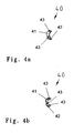
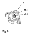
- a multiple contact 40.1 is shown, which is arranged within the base body 10 in a contact holder 30.
- the multiple contact 40.1 in the Fig. 9a is shown formed as hermaphroditic contact element, with two interconnected contact legs - a straight, flat contact leg 44.1 and an approximately S-shaped contact leg 41.1, which is summarized with a Lötfuß 42.1 inserted into a corresponding bore of a printed circuit board.
- a surface mounted version of a multi-contact is provided in the Fig. 9b is shown.
Abstract
Description
Die Erfindung betrifft eine Leiterkartensteckverbindung zur elektrischen Kontaktierung für zwei parallel gegenüberliegende, beabstandete Leiterplatten mit oberflächenmontierbaren Verbindungselementen zum gegenseitigen Ineinandergreifen, die eine Steckseite und eine Lötseite aufweisen.The invention relates to a printed circuit board connector for making electrical contact for two parallel, spaced printed circuit boards with surface-mountable interconnecting elements for mutual engagement having a mating side and a soldering side.
Eine derartige Verbindung wird benötigt, um zwei parallel ausgerichtete Leiterplatten elektrisch mittels einer Steckverbindung zu kontaktieren, wobei die Kontaktierung an beliebigen Stellen von Leiterplatte zu Leiterplatte erfolgen soll und wobei Signale im GHz-Bereich störungssicher zu übertragen sind.Such a connection is required to electrically contact two parallel aligned printed circuit boards by means of a plug-in connection, wherein the contacting is to take place at arbitrary locations from printed circuit board to printed circuit board and wherein signals in the GHz range are to be transmitted without interference.
Leiterkartensteckverbinder für eine "board-to-board" Verbindung sind als kreisförmig ausgeführte Einzelsteckverbinder oder als länglich ausgeführte Reihensteckverbinder mit mehrfach nebeneinander angeordneten Kontakten verfügbar.
Wobei Steckverbindungen mit Einzelkontakten überwiegend als Drehteil ausgeführt sind, deren Herstellung relativ kostenintensiv ist.Circuit board connectors for a "board-to-board" connection are available as circular single connectors or as elongate series connectors with multiple side-by-side contacts.
Wherein plug-in connections with individual contacts are predominantly designed as a turned part, the production of which is relatively expensive.
Aus der
Der Erfindung liegt daher die Aufgabe zugrunde, eine Leiterplattensteckverbindung der eingangs genannten Art dahingehend auszubilden, dass mittels eines kompakten Verbindungselementes, eine hochfrequenzfähige, elektrische Verbindung zwischen zwei Leiterplatten auszugestalten, wobei jedes Verbindungselement oberflächenmontiert mit der Leiterplatte verbunden sein soll.The invention is therefore based on the object to form a printed circuit board connector of the type mentioned in that by means of a compact connection element to design a high-frequency, electrical connection between two circuit boards, each connection element should be surface mounted connected to the circuit board.
Diese Aufgabe wird dadurch gelöst, dass das Verbindungselement einen mehrseitigen symmetrischen, kragenförmigen Grundkörper aufweist, dass in zwei gegenüberliegenden Eckbereichen, einem ersten Eckbereich und einem zweiten Eckbereich des Grundkörpers Kerben vorgesehen sind, und dass innerhalb des Grundkörpers, in einem dritten Eckbereich zwischen den beiden Kerben, eine Kontakthalterung für mindestens einen zum Zentrum des Grundkörpers weisenden elektrischen Signalkontakt vorgesehen ist.This object is achieved in that the connecting element has a multi-sided symmetrical, collar-shaped basic body, that notches are provided in two opposite corner regions, a first corner region and a second corner region of the base body, and that within the base body, in a third corner region between the two notches , a contact holder is provided for at least one pointing to the center of the body electrical signal contact.
Vorteilhafte Ausgestaltungen der Erfindung sind in den Ansprüchen 2-18 angegeben.Advantageous embodiments of the invention are specified in claims 2-18.
Die mit der Erfindung erzielten Vorteile bestehen insbesondere darin, dass mittels der kragenförmigen Struktur des Verbindungselementes, in dessen Innenraum ein isoliert angeordneter, elektrischer Kontakt vorgesehen ist, eine hochfrequenzdichte bis in den GHz-Bereich verwendbare Steckverbindung möglich ist.
Dabei ist das Verbindungselement vorzugsweise als quadratisches, hermaphroditisches Steckteil ausgeführt, das heißt, es ist mit einem baugleichen Steckteil steckbar.
Es sind aber auch weitere, mehrseitige, symmetrisch geformte Verbindungselemente denkbar.
Der aus nichtleitendem Material gefertigte Grundkörper des Verbindungselementes ist komplett von einem elektrisch leitenden Überzug umgeben.The advantages achieved by the invention are, in particular, that by means of the collar-shaped structure of the connecting element, in the interior of which an electrically arranged electrical contact is provided, a high-frequency up to the GHz range usable connector is possible.
In this case, the connecting element is preferably designed as a square, hermaphroditic plug-in part, that is, it can be plugged with a similar plug-in part.
But there are also more, multi-sided, symmetrically shaped fasteners conceivable.
The base body made of non-conductive material of the connecting element is completely surrounded by an electrically conductive coating.
Während im Inneren des Grundkörpers eine elektrisch isolierende Kontakthalterung mit einem darin eingehakten elektrischen Kontakt angeordnet ist, das als separates Bauteil mit entsprechenden gegenseitig wirkenden vorgesehenen Rastmitteln im Grundkörper einsetzbar ist.
Wobei Grundkörper und Kontakthalterung aus thermischen Erwägungen vorteilhafterweise aus dem gleichen isolierenden Material gefertigt sind. Entsprechend ist eine Anordnung der Lötflächen auf den Leiterplatten vorgesehen, so dass der elektrisch leitende Überzug des Verbindungselementes und der Signalkontakt entsprechend getrennten Lötflächen kontaktiert.
In einer Variante kann vorgesehen sein, dass der Grundkörper des Verbindungselementes an wesentlichen Teilen, vorzugsweise im Innenbereich, mit einem elektrisch leitenden Überzug versehen.
Wobei die Kontakthalterung - ohne elektrisch leitenden Überzug - direkt in den Grundkörper eingeformt ist.
Lediglich der innere elektrische Kontakt ist als zusätzliches Bauteil, geformt als Stanzbiegeteil, erforderlich.While inside the body an electrically insulating contact holder is arranged with an electrical contact hooked therein, which can be used as a separate component with corresponding mutually acting locking means provided in the body.
Wherein body and contact holder for thermal considerations are advantageously made of the same insulating material. Accordingly, an arrangement of the solder pads is provided on the circuit boards, so that the electrically conductive coating of the connecting element and the signal contact contacted according to separate pads.
In a variant, it can be provided that the base body of the connecting element is provided with an electrically conductive coating on essential parts, preferably on the inside.
The contact holder - without electrically conductive coating - is molded directly into the main body.
Only the internal electrical contact is required as an additional component, formed as a stamped and bent part.
Zur Erzielung einer hochfrequenzfähigen, abgeschirmten Signalübertragung ist es sinnvoll, die beiden Verbindungselemente ineinandersteckbar auszuführen, so dass optimalerweise eine Art Labyrinthdichtung gebildet wird. Dazu ist der kragenförmige Grundkörper an zwei gegenüberliegenden Eckbereichen mit Kerben versehen, die ein gegenseitiges Ineinanderstecken der beiden identischenverbindungselemente erlauben. Wobei beim Steckvorgang ein Verbindungselement axial um 180° gedreht - seitlich leicht versetzt gegenüber dem anderen - angeordnet ist.To achieve a high-frequency, shielded signal transmission, it makes sense to make the two connecting elements nestable, so that optimally a kind of labyrinth seal is formed. For this purpose, the collar-shaped base body is provided at two opposite corner areas with notches, which allow a mutual nesting of the two identical connecting elements. Wherein during insertion a connecting element is rotated axially by 180 ° - laterally slightly offset from the other - is arranged.
Weiterhin ist steckseitig in dem durch die beiden Kerben eingeschlossenen Eckbereich auf der Kontakthalterung, die den elektrischen Kontakt aufnimmt vorteilhafterweise eine Ansaugfläche vorgesehen, mittels der eine Automatenbestückung des Verbindungselementes auf einer Leiterplatte erfolgen kann.Furthermore, on the plug side, in the corner region enclosed by the two notches, on the contact holder, which receives the electrical contact, a suction surface is advantageously provided, by means of which automatic assembly of the connecting element on a printed circuit board can take place.
Wie bereits oben angedeutet, ist mindestens der Innenbereich, bis auf den isolierenden Bereich des elektrischen Kontaktes, mittels MID-Technik elektrisch leitend beschichtet. Das betrifft auch die beiden Kerben und den mit trichterförmigen Schrägen umlaufenden Kragenrand, sowie den zur Leiterplatte weisenden Kragenrand, in dem vorteilhafterweise Bohrungen vorgesehen sind, die auf das zwischen dem Verbindungselement und der Leiterplatte eingebrachte Lötmittel eine kapillare Wirkung ausüben und eine sichere Lötung bewirken.As already indicated above, at least the inner region, except for the insulating region of the electrical contact, is coated in an electrically conductive manner by means of MID technology. This also applies to the two notches and the circumferential collar edge with funnel-shaped bevels, as well as to the circuit board facing collar edge in which advantageously holes are provided which exert on the introduced between the connecting element and the circuit board solder a capillary action and cause secure soldering.
Der umlaufende, steckseitige Kragenrad weist vorteilhafterweise Schrägen auf, die ein leichteres "Einfangen" zweier zu steckender Verbindungselemente begünstigen, wobei Fehlausrichtungen in der Z-Achse, horizontal gedreht von bis zu +/- 10° tolerierbar für ein Verbindungspaar sind.
Während noch bei einer vertikal geneigten Z-Achse von 7° ein "Einfangen" des Gegensteckers realisierbar ist.
In der Z-Achse, also dem Höhenabstand zwischen zwei Leiterplatten, ist eine Toleranz für den gesteckten Zustand von +/- 0,75 mm vorgesehen.
Da die Verbindungselemente als Kunststoffspritzteile gefertigt werden, ist ein gestufter Abstandsbereich zwischen zwei Leiterplatten von ca. 6 - 30 mm vorgesehen.
Vorzugsweise sind Abstände von 6,7 mm, 19 mm, 28,7 mm vorgesehen. Obwohl als Signalkontakt vorgesehen, ist bei entsprechender Dimensionierung des Verbindungselementes mit dem Signalkontakt durchaus eine Variante als so genannter Power-Kontakt denkbar, wobei auch eine Variante ohne den innenliegenden Signalkontakt realisierbar ist.
Weiterhin ist vorgesehen, Mehrfachkontakte innerhalb des Grundkörpers anzuordnen, die hierbei vorteilhafterweise als hermaphroditische Kontakte ausgebildet sind und einen geraden und einen S-förmigen Kontaktschenkel ausweisen, so dass beim Kontaktieren von zwei entsprechend ausgerüsteten Verbindungselementen, jeweils zwei unterschiedlich geformte Kontaktschenkel miteinander kontaktieren.The circumferential, plug-side collar wheel advantageously has bevels, which favor easier "capture" of two to be connected fasteners, with misalignments in the Z-axis, horizontally rotated by up to +/- 10 ° are tolerable for a connection pair.
While still with a vertically inclined Z-axis of 7 °, a "catching" of the mating connector is feasible.
In the Z-axis, ie the height distance between two printed circuit boards, a tolerance for the inserted state of +/- 0.75 mm is provided.
Since the connecting elements are manufactured as plastic injection molded parts, a stepped distance range between two printed circuit boards of approximately 6 to 30 mm is provided.
Preferably, distances of 6.7 mm, 19 mm, 28.7 mm are provided. Although provided as a signal contact, with appropriate dimensioning of the connecting element with the signal contact quite a variant as a so-called power contact conceivable, with a variant without the internal signal contact can be realized.
Furthermore, it is provided to arrange multiple contacts within the body, which are advantageously designed as hermaphroditic contacts and identify a straight and an S-shaped contact legs, so that contact each other when contacting two appropriately equipped connecting elements, two differently shaped contact legs.
Ein Ausführungsbeispiel der Erfindung ist in der Zeichnung dargestellt und wird im folgenden näher erläutert. Es zeigen:
- Fig. 1
- eine steckseitige, isometrische Darstellung eines Verbindungselementes,
- Fig. 2
- einen lötseitige, isometrische Darstellung des Grundkörpers des Verbindungselementes,
- Fig. 3a
- eine isometrische Darstellung einer Kontakthalterung des Verbindungselementes,
- Fig. 3b
- eine Darstellung der Kontakthalterung mit Ansicht auf den Eckbereich,
- Fig. 3c
- eine Darstellung der Kontakthalterung mit Ansicht auf den Fußbereich,
- Fig. 4a
- eine Darstellung eines elektrischen Kontaktes, Ansicht außen,
- Fig. 4b
- eine Darstellung des elektrischen Kontaktes, Ansicht innen,
- Fig. 5
- eine Variante des Verbindungselementes,
- Fig. 6a
- zwei miteinander gesteckte kurze Verbindungselemente,
- Fig. 6b
- zwei miteinander gesteckte lange Verbindungselemente,
- Fig. 7
- zwei miteinander gesteckte Verbindungselemente ohne Leiterplatten.
- Fig. 8
- ein Verbindungselement mit einem Mehrfach-Kontakt,
- Fig. 9a
- hermaphroditisches Kontaktelement mit Lötfuß,
- Fig. 9b
- hermaphroditisches Kontaktelement ohne Lötfuß, und
- Fig. 10
- eine Variante eines ovalen Verbindungselementes.
- Fig. 1
- a plug-in, isometric view of a connecting element,
- Fig. 2
- a solder-side, isometric view of the main body of the connecting element,
- Fig. 3a
- an isometric view of a contact holder of the connecting element,
- Fig. 3b
- a representation of the contact holder with view on the corner area,
- Fig. 3c
- a representation of the contact holder with view on the foot area,
- Fig. 4a
- a representation of an electrical contact, outside view,
- Fig. 4b
- a representation of the electrical contact, view inside,
- Fig. 5
- a variant of the connecting element,
- Fig. 6a
- two interconnected short connecting elements,
- Fig. 6b
- two interconnected long connecting elements,
- Fig. 7
- two interconnected fasteners without circuit boards.
- Fig. 8
- a connector with a multiple contact,
- Fig. 9a
- hermaphroditic contact element with soldering foot,
- Fig. 9b
- hermaphroditic contact element without solder foot, and
- Fig. 10
- a variant of an oval connecting element.
In der
Das Verbindungselement 1 ist als quadratischer, kragenförmiger Grundkörper 10 geformt, wobei in zwei gegenüberliegenden Eckbereichen 14, 16 jeweils eine senkrecht zum Kragen 11 eingeformte Kerbe 15, 17 vorgesehen ist.
Der gesamte Grundkörper 10 ist mit einer elektrisch leitenden Beschichtung überzogen.In the
The connecting
The
Die Kerbe 15, 17 hat etwa eine Öffnungsweite, die der Kragendicke entspricht und in dieser Darstellung eine Tiefe, die etwa der halben Höhe der gesamten Kragenhöhe entspricht.
In dem von den beiden Kerben 15, 17 eingeschlossenen Eckbereich18, ist innerhalb des Grundkörpers 10 eine aus isolierendem Material geformte Kontakthalterung 30 eingefügt, die zur Aufnahme eines elektrischen Signalkontaktes 40, hier als Einzelkontakt ausgeführt, vorgesehen ist.
Die Kontakthalterung 30 weist zur Steckseite eine hier dreieckförmige Ansaugfläche 31 auf, die als so genannter pick-and-place Punkt ein maschinengesteuertes Platzieren des Verbindungselementes auf einer Leiterplatte erlaubt.
Der Kragen 11 weist einen steckseitigen Kragenrand 12 mit beidseitig nach innen und außen und umlaufend Abschrägungen 20, 21 auf, womit ein leichteres Ineinanderschieben von zwei identischen Verbindungselementen begünstigt wird.The
In the
The
The
An den Eckbereichen 14, 16 sind weiterhin nach außen wirkende Anreihungselemente angeformt, die als Nut 26 und Feder 27 ausgebildet sind. Dabei ist die Feder 27 tonnenförmig mit sich verjüngenden Außenbereichen geformt, so dass bei einer Aneinanderreihung mehrerer Verbindungselemente, zunächst ein leichtes Einfügen der Feder in die Nut erfolgt, bis der dickere Mittelbereich der Nut-Feder-Kombination eine formschlüssige Verbindung ergibt. Dabei ist anzumerken, dass die Nut 26 ebenfalls eine tonnenförmige Längsform mit sich erweiternden Außenbereichen aufweist.At the
Die
Signifikant sind zunächst die beiden T-förmigen Ausnehmungen 19 in den beiden Kragenseiten 11, die den Eckbereich 18 bilden. Hier wird die Kontakthalterung 30 mit entsprechend vorspringenden Rastschienen 32 eingeschoben und gehalten.The
Significant are first the two T-shaped
Weiterhin weist der Eckbereich eine Nut 24 auf, in die ein am Signalkontakt angeformter Lötfuß 42 zum Verlöten auf einem Lötpad auf einer Leiterplatte einsetzbar ist.
Auf dem lötseitigen Kragenrand 13 sind hier zwei Fixierstifte 22 angeformt, die zur Polarisierung und Halterung auf einer Leiterplatte dienen, bis beim Lötvorgang das Lötmittel den Kragenrand und die darin vorgesehenen Bohrungen 23, in die es aufgrund kapillarer Kräfte aufsteigt, endgültig fixiert hat.Furthermore, the corner region has a
On the solder
Die
Wobei in der
Der Grundriss ist entsprechend dem Einfügen in den Eckbereich 18 als dreieckiger Fuß 36 geformt mit einer Höhe die entsprechend der Wandhöhe des Grundkörpers 10 maximal bis an die innere Abschrägung 20 reicht.
Das obere glatte Dreieck ist der Ansaugbereich 31 zur maschinengesteuerten Plazierung des gesamten Verbindungselementes auf einer Leiterplatte vorgesehen.
In der Mitte ist eine säulenähnliche Struktur erkennbar, wobei in der Ausnehmung zwischen den beiden Säulen hier oben ein Durchbruch 33 im unteren Bereich eine Vertiefung 34 und am Fuß eine Tasche 35 ausgebildet ist. Während mit den senkrechten, vorspringen Rastschienen 32 die Fixierung der Kontakthalterung in den T-förmigen Ausnehmungen19 im Grundkörper 10 gewährleistet ist.The
Being in the
The floor plan is formed according to the insertion in the
The upper smooth triangle is the
In the middle of a column-like structure can be seen, in the recess between the two columns up here an
Der in
An drei Positionen, im oberen Schenkelende, im unteren Schenkelende sowie unterhalb des gebogenen Kontaktbereiches sind jeweils dreiseitig freistehende Rasthaken 43 herausgebogen. Mittels dieser Rasthaken wird der Signalkontakt in dem Durchbruch 33, in der Vertiefung 34 und in der Tasche 35 verrastet.The in
At three positions, in the upper leg end, in the lower leg end and below the curved contact area each free-standing three-sided locking hooks 43 are bent out. By means of these latching hook the signal contact in the
Die
In der
Letztlich ist in der
Hier ist eine entsprechende Verlängerung des Signalkontaktes vorgesehen und damit auch eine Verlängerung der Kontakthalterung erforderlich.Ultimately, in the
Here a corresponding extension of the signal contact is provided and thus an extension of the contact holder required.
Die
Deutlich erkennbar ist die Kontaktierung der beiden Signalkontakte 40, die durch den nach außen gebogenen Kontaktbereich 41 eine diagonale Kraftkomponente entwickeln, so dass die Grundkörper 10 der Verbindungselemente stets in die gegenüberliegenden Eckbereiche gedrängt werden und eine ebenso sichere Kontaktierung der Beschichtung zur Übertragung des Massesignals gewährleisten.The
Clearly visible is the contacting of the two
In der
Dabei ist der Mehrfachkontakt 40.1 der in der
Dazu ist auch eine oberflächenmontierbare Version eines Mehrfachkontaktes vorgesehen, die in der
Here is the multiple contact 40.1 in the
For this purpose, a surface mounted version of a multi-contact is provided in the
Letztlich ist in der
Claims (18)
- A circuit board plug connection for an electrical contacting of two circuit boards (3, 5) arranged parallel and opposite to and spaced from each other, including surface-mountable connecting members (1) for mutual engagement which have a plug-in side and a solder side, characterized in that
the connecting member (1) includes a multisided, symmetrical, collar-shaped base body (10),
notches (15, 17) are provided in two opposite corner portions, a first corner portion (14) and a second corner portion (16), of the base body (10), and
within the base body (10), in a third corner portion (18) between the two notches (15, 17), a contact retainer (30) is provided for at least one electrical signal contact (40) facing the center of the base body (10). - The circuit board plug connection according to claim 1, characterized in that
a connecting member (1) is adapted to be plugged with a further connecting member (1) into itself. - The circuit board plug connection according to claim 1, characterized in that
the base body (10) is provided with an electrically conducting coating. - The circuit board plug connection according to claim 1, characterized in that
the contact retainer (30) is adapted to be fixed in place as a separate part in the third corner portion (18) by means of detent rails (32) engaging in cut-outs (19) in the base body (10). - The circuit board plug connection according to claim 1, characterized in that
the opening width of the notches (15, 17) corresponds at least to the wall thickness of the base body (10). - The circuit board plug connection according to claim 1, characterized in that
the plug-in side collar edge (12) of the base body (10) includes inside bevels (20) and outside bevels (21) having different inclinations. - The circuit board plug connection according to claim 1, characterized in that
for a mounting of the base body (10) onto a circuit board (3, 5), a suction area (31) is provided on the contact retainer (30) for a machine-controlled insertion. - The circuit board plug connection according to claim 1, characterized in that
the base body (10) includes a collar (11) having different heights to form different distances between two circuit boards (3, 5). - The circuit board plug connection according to claim 1, characterized in that
the base body (10) has a plurality of boreholes (23) in its solder-side collar edge (13). - The circuit board plug connection according to claim 1, characterized in that
at least one locating pin (22) is molded integrally with the solder-side collar edge (13) of the base body (10). - The circuit board plug connection according to claim 1, characterized in that
for a combination or in-line arrangement of a plurality of connecting members (1), a groove and tongue joint (26, 27) is molded integrally with the first and second corner portions (14, 16) arranged opposite each other. - The circuit board plug connection according to claim 11, characterized in that
the groove and tongue joint (26, 27) each has a barrel-shaped longitudinal formation, the groove (26) having outer portions widening in a funnel shape and the tongue (27) having outer portions tapering on both sides. - The circuit board plug connection according to claim 1, characterized in that
a variant of the connecting member (1') includes an electrically conducting coating applied on the inside of the base body (10) and extending as far as over the plug-in side collar edge (12). - The circuit board plug connection according to claim 13, characterized in that
for the variant of the connecting member (1'), soldering pads (28) are provided in recessed cut-outs (28) on the solder-side collar edge (13) of the base body (10), which are connected to the electrically conducting coating. - The circuit board plug connector according to claim 1, characterized in that
the electrical contact is configured as a single contact (40) or as a multiple contact (40.1), each having a soldering foot (42, 42.2). - The circuit board plug connector according to claim 15, characterized in that
the multiple contact (40.1) is configured hermaphroditically as a bifurcated member, a straight contact leg (44.1) being provided laterally spaced from a contact leg (41.1) bent in an S-shape, and the respective differently shaped contact leg being contacted in the plug-in process. - The circuit board plug connector according to claim 15, characterized in that
a plurality of single contacts (40) and/or multiple contacts (40.1) are arranged within an appropriately shaped base body (10). - The circuit board plug connector according to claim 15, characterized in that
the electrical contact (40, 40.2) is configured as a surface-solderable contact.
Applications Claiming Priority (1)
| Application Number | Priority Date | Filing Date | Title |
|---|---|---|---|
| DE102007006204A DE102007006204B3 (en) | 2007-02-08 | 2007-02-08 | Conductor card pad connection for printed circuit board, has single-piece, surface-mounted connection unit formed as quadratic, multi-sided symmetrical base body, and notches provided between two edge areas |
Publications (3)
| Publication Number | Publication Date |
|---|---|
| EP1973201A2 EP1973201A2 (en) | 2008-09-24 |
| EP1973201A3 EP1973201A3 (en) | 2010-06-02 |
| EP1973201B1 true EP1973201B1 (en) | 2011-07-27 |
Family
ID=39185274
Family Applications (1)
| Application Number | Title | Priority Date | Filing Date |
|---|---|---|---|
| EP08001989A Active EP1973201B1 (en) | 2007-02-08 | 2008-02-02 | Circuit board connector for two parallel circuit boards |
Country Status (7)
| Country | Link |
|---|---|
| US (1) | US7513780B2 (en) |
| EP (1) | EP1973201B1 (en) |
| JP (1) | JP4709863B2 (en) |
| CN (1) | CN101242039B (en) |
| AT (1) | ATE518278T1 (en) |
| DE (1) | DE102007006204B3 (en) |
| ES (1) | ES2369025T3 (en) |
Cited By (1)
| Publication number | Priority date | Publication date | Assignee | Title |
|---|---|---|---|---|
| US11316295B2 (en) | 2018-04-17 | 2022-04-26 | ept Holding GmbH & Co. KG | Connector part having hermaphroditic contact elements |
Families Citing this family (6)
| Publication number | Priority date | Publication date | Assignee | Title |
|---|---|---|---|---|
| CH701206A2 (en) * | 2009-06-02 | 2010-12-15 | Huber+Suhner Ag | Printed circuit board assembly. |
| WO2011091691A1 (en) * | 2010-01-29 | 2011-08-04 | 华为技术有限公司 | Electromagnetic shielding method and device |
| CN202004200U (en) * | 2011-01-06 | 2011-10-05 | 富士康(昆山)电脑接插件有限公司 | Electric connector assembly |
| DE102011055750B3 (en) * | 2011-11-28 | 2013-02-14 | Harting Kgaa | Insulator of a connector |
| US9614334B2 (en) * | 2014-10-31 | 2017-04-04 | Microsoft Technology Licensing, Llc | Hermaphroditic electrical connector |
| CN105514728A (en) * | 2016-01-05 | 2016-04-20 | 陈烁 | Connecting plug |
Family Cites Families (14)
| Publication number | Priority date | Publication date | Assignee | Title |
|---|---|---|---|---|
| US5156553A (en) * | 1990-05-29 | 1992-10-20 | Kel Corporation | Connector assembly for film circuitry |
| US5055054A (en) * | 1990-06-05 | 1991-10-08 | E. I. Du Pont De Nemours And Company | High density connector |
| JP2564112Y2 (en) * | 1991-01-11 | 1998-03-04 | ソニー株式会社 | connector |
| FR2677816B1 (en) * | 1991-06-17 | 1995-04-28 | Radiall Sa | COAXIAL CONNECTOR FOR THE CONNECTION OF A COAXIAL CABLE TO A PRINTED ELECTRONIC CIRCUIT BOARD. |
| US5161985A (en) * | 1991-08-08 | 1992-11-10 | Robinson Nugent, Inc. | Board to board interconnect |
| JP2526663Y2 (en) * | 1991-08-09 | 1997-02-19 | 日本航空電子工業株式会社 | connector |
| US5181855A (en) * | 1991-10-03 | 1993-01-26 | Itt Corporation | Simplified contact connector system |
| JPH07161415A (en) * | 1993-12-02 | 1995-06-23 | Amp Japan Ltd | Electric connector and electric contact using this connector |
| US5498167A (en) * | 1994-04-13 | 1996-03-12 | Molex Incorporated | Board to board electrical connectors |
| JPH07326430A (en) * | 1994-05-31 | 1995-12-12 | Amp Japan Ltd | Electric connector and contact for use therewith |
| US6752637B2 (en) * | 2001-02-06 | 2004-06-22 | Ford Global Technologies, Llc | Flexible circuit relay |
| JP2006066384A (en) * | 2004-07-27 | 2006-03-09 | Hosiden Corp | Coaxial connector for board-to-board connection |
| CN2772061Y (en) * | 2005-02-04 | 2006-04-12 | 上海莫仕连接器有限公司 | Electrical connector assembly |
| TWM284091U (en) * | 2005-04-21 | 2005-12-21 | Molex Taiwan Ltd | Electrical connector |
-
2007
- 2007-02-08 DE DE102007006204A patent/DE102007006204B3/en not_active Expired - Fee Related
-
2008
- 2008-01-24 US US12/019,580 patent/US7513780B2/en active Active
- 2008-02-02 AT AT08001989T patent/ATE518278T1/en active
- 2008-02-02 EP EP08001989A patent/EP1973201B1/en active Active
- 2008-02-02 ES ES08001989T patent/ES2369025T3/en active Active
- 2008-02-04 CN CN2008100048378A patent/CN101242039B/en active Active
- 2008-02-08 JP JP2008028931A patent/JP4709863B2/en not_active Expired - Fee Related
Cited By (1)
| Publication number | Priority date | Publication date | Assignee | Title |
|---|---|---|---|---|
| US11316295B2 (en) | 2018-04-17 | 2022-04-26 | ept Holding GmbH & Co. KG | Connector part having hermaphroditic contact elements |
Also Published As
| Publication number | Publication date |
|---|---|
| CN101242039A (en) | 2008-08-13 |
| ATE518278T1 (en) | 2011-08-15 |
| JP4709863B2 (en) | 2011-06-29 |
| DE102007006204B3 (en) | 2008-04-17 |
| US7513780B2 (en) | 2009-04-07 |
| US20080194125A1 (en) | 2008-08-14 |
| EP1973201A3 (en) | 2010-06-02 |
| EP1973201A2 (en) | 2008-09-24 |
| JP2008198606A (en) | 2008-08-28 |
| ES2369025T3 (en) | 2011-11-24 |
| CN101242039B (en) | 2010-12-15 |
Similar Documents
| Publication | Publication Date | Title |
|---|---|---|
| EP1973201B1 (en) | Circuit board connector for two parallel circuit boards | |
| DE19751970C2 (en) | PCB connector | |
| DE19753839C1 (en) | For coaxial angle plug-type connection unit | |
| DE19736607C1 (en) | PCB socket | |
| DE19705509C2 (en) | One-piece contact spring | |
| EP2639894B1 (en) | Electrical connector with tolerance compensation | |
| EP1575131A1 (en) | Electrical connector | |
| EP2862237B1 (en) | Insulating body of a plug-in connector | |
| DE112013006540T5 (en) | Connector with staggered contacts | |
| EP1109259B1 (en) | Electrical connector for circuit board | |
| EP1429423B1 (en) | Electrical plug connector having a casing and a heavy current contact | |
| DE102012105257B4 (en) | Insulator of a connector | |
| DE3926802A1 (en) | ELECTRICAL CONNECTOR | |
| DE3810209C2 (en) | ||
| EP2561582B1 (en) | Electrical plug contact | |
| EP2690721A1 (en) | Electrical connector assembly soldered on a circuit board with tolerance compensation | |
| EP3714514B1 (en) | Plug-type connector | |
| DE102017115914B3 (en) | Printed circuit board connector with a screen element | |
| EP1111723B1 (en) | Socket for plugconnections | |
| DE10204842B4 (en) | PC Board | |
| DE102018112170A1 (en) | Contact device with a fork | |
| DE102019111193B3 (en) | Interface with PCB contact for PCB | |
| DE102007043887A1 (en) | Connector with integrated circuit board | |
| DE10047126B4 (en) | fastening device | |
| EP1149436B1 (en) | Hf right-angle coaxial connector element |
Legal Events
| Date | Code | Title | Description |
|---|---|---|---|
| PUAI | Public reference made under article 153(3) epc to a published international application that has entered the european phase |
Free format text: ORIGINAL CODE: 0009012 |
|
| AK | Designated contracting states |
Kind code of ref document: A2 Designated state(s): AT BE BG CH CY CZ DE DK EE ES FI FR GB GR HR HU IE IS IT LI LT LU LV MC MT NL NO PL PT RO SE SI SK TR |
|
| AX | Request for extension of the european patent |
Extension state: AL BA MK RS |
|
| PUAL | Search report despatched |
Free format text: ORIGINAL CODE: 0009013 |
|
| AK | Designated contracting states |
Kind code of ref document: A3 Designated state(s): AT BE BG CH CY CZ DE DK EE ES FI FR GB GR HR HU IE IS IT LI LT LU LV MC MT NL NO PL PT RO SE SI SK TR |
|
| AX | Request for extension of the european patent |
Extension state: AL BA MK RS |
|
| RIC1 | Information provided on ipc code assigned before grant |
Ipc: H01R 13/28 20060101ALI20100423BHEP Ipc: H01R 13/658 20060101ALN20100423BHEP Ipc: H01R 12/16 20060101AFI20080820BHEP |
|
| 17P | Request for examination filed |
Effective date: 20100809 |
|
| AKX | Designation fees paid |
Designated state(s): AT BE BG CH CY CZ DE DK EE ES FI FR GB GR HR HU IE IS IT LI LT LU LV MC MT NL NO PL PT RO SE SI SK TR |
|
| REG | Reference to a national code |
Ref country code: DE Ref legal event code: R079 Ref document number: 502008004300 Country of ref document: DE Free format text: PREVIOUS MAIN CLASS: H01R0012160000 Ipc: H01R0012710000 |
|
| GRAP | Despatch of communication of intention to grant a patent |
Free format text: ORIGINAL CODE: EPIDOSNIGR1 |
|
| RIC1 | Information provided on ipc code assigned before grant |
Ipc: H01R 13/658 20110101ALN20110302BHEP Ipc: H01R 12/71 20110101AFI20110302BHEP Ipc: H01R 13/28 20060101ALI20110302BHEP |
|
| GRAS | Grant fee paid |
Free format text: ORIGINAL CODE: EPIDOSNIGR3 |
|
| GRAA | (expected) grant |
Free format text: ORIGINAL CODE: 0009210 |
|
| AK | Designated contracting states |
Kind code of ref document: B1 Designated state(s): AT BE BG CH CY CZ DE DK EE ES FI FR GB GR HR HU IE IS IT LI LT LU LV MC MT NL NO PL PT RO SE SI SK TR |
|
| REG | Reference to a national code |
Ref country code: GB Ref legal event code: FG4D Free format text: NOT ENGLISH |
|
| REG | Reference to a national code |
Ref country code: CH Ref legal event code: EP |
|
| REG | Reference to a national code |
Ref country code: DE Ref legal event code: R096 Ref document number: 502008004300 Country of ref document: DE Effective date: 20110915 |
|
| REG | Reference to a national code |
Ref country code: SE Ref legal event code: TRGR |
|
| REG | Reference to a national code |
Ref country code: NL Ref legal event code: T3 |
|
| REG | Reference to a national code |
Ref country code: ES Ref legal event code: FG2A Ref document number: 2369025 Country of ref document: ES Kind code of ref document: T3 Effective date: 20111124 |
|
| PG25 | Lapsed in a contracting state [announced via postgrant information from national office to epo] |
Ref country code: PT Free format text: LAPSE BECAUSE OF FAILURE TO SUBMIT A TRANSLATION OF THE DESCRIPTION OR TO PAY THE FEE WITHIN THE PRESCRIBED TIME-LIMIT Effective date: 20111128 Ref country code: NO Free format text: LAPSE BECAUSE OF FAILURE TO SUBMIT A TRANSLATION OF THE DESCRIPTION OR TO PAY THE FEE WITHIN THE PRESCRIBED TIME-LIMIT Effective date: 20111027 Ref country code: HR Free format text: LAPSE BECAUSE OF FAILURE TO SUBMIT A TRANSLATION OF THE DESCRIPTION OR TO PAY THE FEE WITHIN THE PRESCRIBED TIME-LIMIT Effective date: 20110727 Ref country code: LT Free format text: LAPSE BECAUSE OF FAILURE TO SUBMIT A TRANSLATION OF THE DESCRIPTION OR TO PAY THE FEE WITHIN THE PRESCRIBED TIME-LIMIT Effective date: 20110727 Ref country code: IS Free format text: LAPSE BECAUSE OF FAILURE TO SUBMIT A TRANSLATION OF THE DESCRIPTION OR TO PAY THE FEE WITHIN THE PRESCRIBED TIME-LIMIT Effective date: 20111127 |
|
| PG25 | Lapsed in a contracting state [announced via postgrant information from national office to epo] |
Ref country code: SI Free format text: LAPSE BECAUSE OF FAILURE TO SUBMIT A TRANSLATION OF THE DESCRIPTION OR TO PAY THE FEE WITHIN THE PRESCRIBED TIME-LIMIT Effective date: 20110727 Ref country code: PL Free format text: LAPSE BECAUSE OF FAILURE TO SUBMIT A TRANSLATION OF THE DESCRIPTION OR TO PAY THE FEE WITHIN THE PRESCRIBED TIME-LIMIT Effective date: 20110727 Ref country code: LV Free format text: LAPSE BECAUSE OF FAILURE TO SUBMIT A TRANSLATION OF THE DESCRIPTION OR TO PAY THE FEE WITHIN THE PRESCRIBED TIME-LIMIT Effective date: 20110727 Ref country code: GR Free format text: LAPSE BECAUSE OF FAILURE TO SUBMIT A TRANSLATION OF THE DESCRIPTION OR TO PAY THE FEE WITHIN THE PRESCRIBED TIME-LIMIT Effective date: 20111028 Ref country code: CY Free format text: LAPSE BECAUSE OF FAILURE TO SUBMIT A TRANSLATION OF THE DESCRIPTION OR TO PAY THE FEE WITHIN THE PRESCRIBED TIME-LIMIT Effective date: 20110727 |
|
| REG | Reference to a national code |
Ref country code: IE Ref legal event code: FD4D |
|
| PG25 | Lapsed in a contracting state [announced via postgrant information from national office to epo] |
Ref country code: IE Free format text: LAPSE BECAUSE OF FAILURE TO SUBMIT A TRANSLATION OF THE DESCRIPTION OR TO PAY THE FEE WITHIN THE PRESCRIBED TIME-LIMIT Effective date: 20110727 Ref country code: CZ Free format text: LAPSE BECAUSE OF FAILURE TO SUBMIT A TRANSLATION OF THE DESCRIPTION OR TO PAY THE FEE WITHIN THE PRESCRIBED TIME-LIMIT Effective date: 20110727 Ref country code: SK Free format text: LAPSE BECAUSE OF FAILURE TO SUBMIT A TRANSLATION OF THE DESCRIPTION OR TO PAY THE FEE WITHIN THE PRESCRIBED TIME-LIMIT Effective date: 20110727 |
|
| PGFP | Annual fee paid to national office [announced via postgrant information from national office to epo] |
Ref country code: CH Payment date: 20120227 Year of fee payment: 5 |
|
| PG25 | Lapsed in a contracting state [announced via postgrant information from national office to epo] |
Ref country code: RO Free format text: LAPSE BECAUSE OF FAILURE TO SUBMIT A TRANSLATION OF THE DESCRIPTION OR TO PAY THE FEE WITHIN THE PRESCRIBED TIME-LIMIT Effective date: 20110727 Ref country code: EE Free format text: LAPSE BECAUSE OF FAILURE TO SUBMIT A TRANSLATION OF THE DESCRIPTION OR TO PAY THE FEE WITHIN THE PRESCRIBED TIME-LIMIT Effective date: 20110727 |
|
| PLBE | No opposition filed within time limit |
Free format text: ORIGINAL CODE: 0009261 |
|
| STAA | Information on the status of an ep patent application or granted ep patent |
Free format text: STATUS: NO OPPOSITION FILED WITHIN TIME LIMIT |
|
| PG25 | Lapsed in a contracting state [announced via postgrant information from national office to epo] |
Ref country code: DK Free format text: LAPSE BECAUSE OF FAILURE TO SUBMIT A TRANSLATION OF THE DESCRIPTION OR TO PAY THE FEE WITHIN THE PRESCRIBED TIME-LIMIT Effective date: 20110727 |
|
| PGFP | Annual fee paid to national office [announced via postgrant information from national office to epo] |
Ref country code: GB Payment date: 20120221 Year of fee payment: 5 Ref country code: FI Payment date: 20120221 Year of fee payment: 5 Ref country code: SE Payment date: 20120221 Year of fee payment: 5 Ref country code: IT Payment date: 20120223 Year of fee payment: 5 |
|
| 26N | No opposition filed |
Effective date: 20120502 |
|
| PGFP | Annual fee paid to national office [announced via postgrant information from national office to epo] |
Ref country code: NL Payment date: 20120229 Year of fee payment: 5 |
|
| REG | Reference to a national code |
Ref country code: DE Ref legal event code: R097 Ref document number: 502008004300 Country of ref document: DE Effective date: 20120502 |
|
| BERE | Be: lapsed |
Owner name: HARTING ELECTRONICS G.M.B.H. & CO. KG Effective date: 20120228 |
|
| PG25 | Lapsed in a contracting state [announced via postgrant information from national office to epo] |
Ref country code: MC Free format text: LAPSE BECAUSE OF NON-PAYMENT OF DUE FEES Effective date: 20120229 |
|
| PG25 | Lapsed in a contracting state [announced via postgrant information from national office to epo] |
Ref country code: BE Free format text: LAPSE BECAUSE OF NON-PAYMENT OF DUE FEES Effective date: 20120228 |
|
| PG25 | Lapsed in a contracting state [announced via postgrant information from national office to epo] |
Ref country code: BG Free format text: LAPSE BECAUSE OF FAILURE TO SUBMIT A TRANSLATION OF THE DESCRIPTION OR TO PAY THE FEE WITHIN THE PRESCRIBED TIME-LIMIT Effective date: 20111027 |
|
| PGFP | Annual fee paid to national office [announced via postgrant information from national office to epo] |
Ref country code: ES Payment date: 20120213 Year of fee payment: 5 |
|
| PG25 | Lapsed in a contracting state [announced via postgrant information from national office to epo] |
Ref country code: MT Free format text: LAPSE BECAUSE OF FAILURE TO SUBMIT A TRANSLATION OF THE DESCRIPTION OR TO PAY THE FEE WITHIN THE PRESCRIBED TIME-LIMIT Effective date: 20110727 |
|
| REG | Reference to a national code |
Ref country code: NL Ref legal event code: V1 Effective date: 20130901 |
|
| REG | Reference to a national code |
Ref country code: CH Ref legal event code: PL |
|
| REG | Reference to a national code |
Ref country code: SE Ref legal event code: EUG |
|
| GBPC | Gb: european patent ceased through non-payment of renewal fee |
Effective date: 20130202 |
|
| PG25 | Lapsed in a contracting state [announced via postgrant information from national office to epo] |
Ref country code: CH Free format text: LAPSE BECAUSE OF NON-PAYMENT OF DUE FEES Effective date: 20130228 Ref country code: NL Free format text: LAPSE BECAUSE OF NON-PAYMENT OF DUE FEES Effective date: 20130901 Ref country code: FI Free format text: LAPSE BECAUSE OF NON-PAYMENT OF DUE FEES Effective date: 20130202 Ref country code: LI Free format text: LAPSE BECAUSE OF NON-PAYMENT OF DUE FEES Effective date: 20130228 Ref country code: SE Free format text: LAPSE BECAUSE OF NON-PAYMENT OF DUE FEES Effective date: 20130203 |
|
| PG25 | Lapsed in a contracting state [announced via postgrant information from national office to epo] |
Ref country code: IT Free format text: LAPSE BECAUSE OF NON-PAYMENT OF DUE FEES Effective date: 20130202 |
|
| PG25 | Lapsed in a contracting state [announced via postgrant information from national office to epo] |
Ref country code: GB Free format text: LAPSE BECAUSE OF NON-PAYMENT OF DUE FEES Effective date: 20130202 |
|
| REG | Reference to a national code |
Ref country code: ES Ref legal event code: FD2A Effective date: 20140408 |
|
| REG | Reference to a national code |
Ref country code: AT Ref legal event code: MM01 Ref document number: 518278 Country of ref document: AT Kind code of ref document: T Effective date: 20130202 |
|
| PG25 | Lapsed in a contracting state [announced via postgrant information from national office to epo] |
Ref country code: TR Free format text: LAPSE BECAUSE OF FAILURE TO SUBMIT A TRANSLATION OF THE DESCRIPTION OR TO PAY THE FEE WITHIN THE PRESCRIBED TIME-LIMIT Effective date: 20110727 |
|
| PG25 | Lapsed in a contracting state [announced via postgrant information from national office to epo] |
Ref country code: LU Free format text: LAPSE BECAUSE OF NON-PAYMENT OF DUE FEES Effective date: 20120202 Ref country code: AT Free format text: LAPSE BECAUSE OF NON-PAYMENT OF DUE FEES Effective date: 20130202 |
|
| PG25 | Lapsed in a contracting state [announced via postgrant information from national office to epo] |
Ref country code: HU Free format text: LAPSE BECAUSE OF FAILURE TO SUBMIT A TRANSLATION OF THE DESCRIPTION OR TO PAY THE FEE WITHIN THE PRESCRIBED TIME-LIMIT Effective date: 20080202 |
|
| PG25 | Lapsed in a contracting state [announced via postgrant information from national office to epo] |
Ref country code: ES Free format text: LAPSE BECAUSE OF NON-PAYMENT OF DUE FEES Effective date: 20130203 |
|
| REG | Reference to a national code |
Ref country code: FR Ref legal event code: PLFP Year of fee payment: 8 |
|
| REG | Reference to a national code |
Ref country code: FR Ref legal event code: PLFP Year of fee payment: 9 |
|
| REG | Reference to a national code |
Ref country code: DE Ref legal event code: R081 Ref document number: 502008004300 Country of ref document: DE Owner name: HARTING ELECTRONICS GMBH, DE Free format text: FORMER OWNER: HARTING ELECTRONICS GMBH & CO. KG, 32339 ESPELKAMP, DE |
|
| REG | Reference to a national code |
Ref country code: FR Ref legal event code: PLFP Year of fee payment: 10 |
|
| REG | Reference to a national code |
Ref country code: FR Ref legal event code: PLFP Year of fee payment: 11 |
|
| PGFP | Annual fee paid to national office [announced via postgrant information from national office to epo] |
Ref country code: FR Payment date: 20230223 Year of fee payment: 16 |
|
| PGFP | Annual fee paid to national office [announced via postgrant information from national office to epo] |
Ref country code: DE Payment date: 20230227 Year of fee payment: 16 |
|
| P01 | Opt-out of the competence of the unified patent court (upc) registered |
Effective date: 20230603 |