JP4709863B2 - Printed circuit board card insertion connection for two parallel printed circuit boards - Google Patents
Printed circuit board card insertion connection for two parallel printed circuit boards Download PDFInfo
- Publication number
- JP4709863B2 JP4709863B2 JP2008028931A JP2008028931A JP4709863B2 JP 4709863 B2 JP4709863 B2 JP 4709863B2 JP 2008028931 A JP2008028931 A JP 2008028931A JP 2008028931 A JP2008028931 A JP 2008028931A JP 4709863 B2 JP4709863 B2 JP 4709863B2
- Authority
- JP
- Japan
- Prior art keywords
- contact
- printed circuit
- collar
- circuit board
- connection
- Prior art date
- Legal status (The legal status is an assumption and is not a legal conclusion. Google has not performed a legal analysis and makes no representation as to the accuracy of the status listed.)
- Expired - Fee Related
Links
Images


Classifications
-
- H—ELECTRICITY
- H01—ELECTRIC ELEMENTS
- H01R—ELECTRICALLY-CONDUCTIVE CONNECTIONS; STRUCTURAL ASSOCIATIONS OF A PLURALITY OF MUTUALLY-INSULATED ELECTRICAL CONNECTING ELEMENTS; COUPLING DEVICES; CURRENT COLLECTORS
- H01R24/00—Two-part coupling devices, or either of their cooperating parts, characterised by their overall structure
- H01R24/84—Hermaphroditic coupling devices
-
- H—ELECTRICITY
- H01—ELECTRIC ELEMENTS
- H01R—ELECTRICALLY-CONDUCTIVE CONNECTIONS; STRUCTURAL ASSOCIATIONS OF A PLURALITY OF MUTUALLY-INSULATED ELECTRICAL CONNECTING ELEMENTS; COUPLING DEVICES; CURRENT COLLECTORS
- H01R12/00—Structural associations of a plurality of mutually-insulated electrical connecting elements, specially adapted for printed circuits, e.g. printed circuit boards [PCB], flat or ribbon cables, or like generally planar structures, e.g. terminal strips, terminal blocks; Coupling devices specially adapted for printed circuits, flat or ribbon cables, or like generally planar structures; Terminals specially adapted for contact with, or insertion into, printed circuits, flat or ribbon cables, or like generally planar structures
- H01R12/70—Coupling devices
- H01R12/71—Coupling devices for rigid printing circuits or like structures
- H01R12/72—Coupling devices for rigid printing circuits or like structures coupling with the edge of the rigid printed circuits or like structures
- H01R12/73—Coupling devices for rigid printing circuits or like structures coupling with the edge of the rigid printed circuits or like structures connecting to other rigid printed circuits or like structures
-
- H—ELECTRICITY
- H01—ELECTRIC ELEMENTS
- H01R—ELECTRICALLY-CONDUCTIVE CONNECTIONS; STRUCTURAL ASSOCIATIONS OF A PLURALITY OF MUTUALLY-INSULATED ELECTRICAL CONNECTING ELEMENTS; COUPLING DEVICES; CURRENT COLLECTORS
- H01R12/00—Structural associations of a plurality of mutually-insulated electrical connecting elements, specially adapted for printed circuits, e.g. printed circuit boards [PCB], flat or ribbon cables, or like generally planar structures, e.g. terminal strips, terminal blocks; Coupling devices specially adapted for printed circuits, flat or ribbon cables, or like generally planar structures; Terminals specially adapted for contact with, or insertion into, printed circuits, flat or ribbon cables, or like generally planar structures
- H01R12/50—Fixed connections
- H01R12/51—Fixed connections for rigid printed circuits or like structures
- H01R12/52—Fixed connections for rigid printed circuits or like structures connecting to other rigid printed circuits or like structures
-
- H—ELECTRICITY
- H01—ELECTRIC ELEMENTS
- H01R—ELECTRICALLY-CONDUCTIVE CONNECTIONS; STRUCTURAL ASSOCIATIONS OF A PLURALITY OF MUTUALLY-INSULATED ELECTRICAL CONNECTING ELEMENTS; COUPLING DEVICES; CURRENT COLLECTORS
- H01R12/00—Structural associations of a plurality of mutually-insulated electrical connecting elements, specially adapted for printed circuits, e.g. printed circuit boards [PCB], flat or ribbon cables, or like generally planar structures, e.g. terminal strips, terminal blocks; Coupling devices specially adapted for printed circuits, flat or ribbon cables, or like generally planar structures; Terminals specially adapted for contact with, or insertion into, printed circuits, flat or ribbon cables, or like generally planar structures
- H01R12/50—Fixed connections
- H01R12/51—Fixed connections for rigid printed circuits or like structures
- H01R12/55—Fixed connections for rigid printed circuits or like structures characterised by the terminals
- H01R12/57—Fixed connections for rigid printed circuits or like structures characterised by the terminals surface mounting terminals
-
- H—ELECTRICITY
- H01—ELECTRIC ELEMENTS
- H01R—ELECTRICALLY-CONDUCTIVE CONNECTIONS; STRUCTURAL ASSOCIATIONS OF A PLURALITY OF MUTUALLY-INSULATED ELECTRICAL CONNECTING ELEMENTS; COUPLING DEVICES; CURRENT COLLECTORS
- H01R13/00—Details of coupling devices of the kinds covered by groups H01R12/70 or H01R24/00 - H01R33/00
- H01R13/02—Contact members
- H01R13/28—Contacts for sliding cooperation with identically-shaped contact, e.g. for hermaphroditic coupling devices
-
- H—ELECTRICITY
- H01—ELECTRIC ELEMENTS
- H01R—ELECTRICALLY-CONDUCTIVE CONNECTIONS; STRUCTURAL ASSOCIATIONS OF A PLURALITY OF MUTUALLY-INSULATED ELECTRICAL CONNECTING ELEMENTS; COUPLING DEVICES; CURRENT COLLECTORS
- H01R13/00—Details of coupling devices of the kinds covered by groups H01R12/70 or H01R24/00 - H01R33/00
- H01R13/648—Protective earth or shield arrangements on coupling devices, e.g. anti-static shielding
- H01R13/658—High frequency shielding arrangements, e.g. against EMI [Electro-Magnetic Interference] or EMP [Electro-Magnetic Pulse]
- H01R13/6598—Shield material
- H01R13/6599—Dielectric material made conductive, e.g. plastic material coated with metal
-
- H—ELECTRICITY
- H01—ELECTRIC ELEMENTS
- H01R—ELECTRICALLY-CONDUCTIVE CONNECTIONS; STRUCTURAL ASSOCIATIONS OF A PLURALITY OF MUTUALLY-INSULATED ELECTRICAL CONNECTING ELEMENTS; COUPLING DEVICES; CURRENT COLLECTORS
- H01R24/00—Two-part coupling devices, or either of their cooperating parts, characterised by their overall structure
- H01R24/38—Two-part coupling devices, or either of their cooperating parts, characterised by their overall structure having concentrically or coaxially arranged contacts
- H01R24/40—Two-part coupling devices, or either of their cooperating parts, characterised by their overall structure having concentrically or coaxially arranged contacts specially adapted for high frequency
- H01R24/50—Two-part coupling devices, or either of their cooperating parts, characterised by their overall structure having concentrically or coaxially arranged contacts specially adapted for high frequency mounted on a PCB [Printed Circuit Board]
Abstract
Description
本発明は、平行に相互に対向して離隔されている2つのプリント基板で電気的にコンタクトを行うためのプリント基板カード差込接続部に関する。これら2つのプリント基板は、相互に係合するための表面実装型の接続エレメントを有し、これらは差込側とはんだ側とを有する。 The present invention relates to a printed circuit board card plug-in connection portion for making electrical contact between two printed circuit boards that are spaced apart from each other in parallel. These two printed circuit boards have surface-mounting connection elements for engaging each other, which have a plug-in side and a solder side.
このような接続部は、平行に方向づけされた2つのプリント基板を差込接続部によって電気的にコンタクトするために必要とされる。このコンタクトは、プリント基板ごとに任意の位置で行わなければならず、GHz領域にある信号を耐妨害性に伝送しなければならない。 Such a connection is required to electrically contact two printed circuit boards oriented in parallel by the plug-in connection. This contact must be made at an arbitrary position for each printed circuit board, and signals in the GHz range must be transmitted in an interference-resistant manner.
US7118383B2から、2つのプリント基板を接続するための同軸差込コネクタが公知である。この同軸差込コネクタでは、管形の2つの表面実装型の差込ボディを相互に差し込み、一方の差込ボディのピン形の中心コンタクトを、他方の差込ボディのU形の相手側のコンタクトに係合させる。 US Pat. No. 7,118,383 B2 discloses a coaxial plug connector for connecting two printed circuit boards. In this coaxial plug connector, two tube-type surface-mount plug-in bodies are inserted into each other, the pin-shaped center contact of one plug-in body is connected to the U-shaped mating contact of the other plug-in body Engage with.
「ボードツーボード」接続用のプリント基板カードコネクタは、環形に形成されたシングル差込コネクタとして提供されるか、または、多重に連続的に配置されたコンタクトを有する細長く形成された直列差込コネクタとして提供されている。 Printed circuit board card connectors for "board-to-board" connections are provided as ring-shaped single plug connectors or elongated serial plug connectors with multiple consecutively arranged contacts Is offered as.
シングルコンタクトを有する差込接続部は主に回転部分として形成されており、この製造は比較的高コストである。 The plug-in connection with a single contact is mainly formed as a rotating part, and its production is relatively expensive.
本発明の課題は、冒頭に述べた形式のプリント基板カード接続部を次のように構成すること、すなわち、コンパクトな接続エレメントによって、高周波動作可能な電気的接続部を2つのプリント基板間に形成し、各接続エレメントは表面実装で該プリント基板に接続されるように構成することである。 An object of the present invention is to form a printed circuit board card connecting portion of the type described at the beginning as follows, that is, an electrical connecting portion capable of high-frequency operation is formed between two printed circuit boards by a compact connecting element. Each connection element is configured to be connected to the printed circuit board by surface mounting.
前記課題は、接続エレメントが、多面体形かつ対称的であるカラー形のボディを有し、該ボディの2つの対向するコーナ領域である第1のコーナ領域と第2のコーナ領域とにノッチが設けられており、該ボディ内部において両ノッチの間の第3の領域に、該ボディの中心を向いている少なくとも1つの電気的な信号コンタクトに対するコンタクトホルダが設けられている構成によって解決される。 The problem is that the connecting element has a polyhedral and symmetrical collar-shaped body, and the first and second corner areas, which are two opposing corner areas of the body, are provided with notches. This is solved by a configuration in which a contact holder for at least one electrical signal contact facing the center of the body is provided in the third region between the notches inside the body.
請求項2〜18に本発明の有利な実施形態が記載されている。 Claims 2 to 18 describe advantageous embodiments of the invention.
本発明によって実現される利点はとりわけ、内部空間に絶縁されて配置された電気的コンタクトを有する、前記接続エレメントのカラー形の構造体によって、GHz領域まで使用可能な耐高周波性の差込接続部を実現できることである。 The advantages realized by the present invention are, among other things, a high-frequency-resistant plug-in connection which can be used up to the GHz range by means of the collar-shaped structure of the connection element, which has an electrical contact arranged insulated in the interior space. Can be realized.
ここでは、接続エレメントは有利には、正方形の雌雄両性の差込部分として形成される。すなわちこの接続エレメントは、同じ形状の差込部分によって差込可能に形成される。 Here, the connecting element is advantageously formed as a square male and female plug. In other words, the connection element is formed so as to be insertable by an insertion portion having the same shape.
また、対称的に成形された多面体形の別の接続エレメントも考えられる。 Also possible are other connecting elements which are symmetrically shaped polyhedral.
非導電性の材料から製造された接続エレメントのボディは、導電性のカバーによって完全に包囲される。 The body of the connecting element made from a non-conductive material is completely surrounded by a conductive cover.
ボディの内部に電気的に絶縁性のコンタクトホルダが配置されており、該コンタクトホルダに電気的なコンタクトが係合される。これは、相互作用するように適切に形成された係止手段を有する別個の部分として、ボディ内で使用される。ここでは、ボディおよびコンタクトホルダは熱的な配慮から、有利には同一の絶縁性材料から製造される。これに相応して、はんだ面の構成体がプリント基板上に設けられ、接続エレメントの導電性のカバーおよび信号コンタクトは、別個のはんだ面にしたがってコンタクトするように構成される。1つの実施形態では、接続エレメントのボディの重要な部分に、有利には内部領域に、導電性のカバーが設けられる。ここではコンタクトホルダは、導電性のカバーなしでボディに直接成形される。 An electrically insulating contact holder is disposed inside the body, and the electrical contact is engaged with the contact holder. This is used in the body as a separate part with locking means suitably shaped to interact. Here, the body and the contact holder are preferably manufactured from the same insulative material due to thermal considerations. Correspondingly, a solder surface structure is provided on the printed circuit board, and the conductive cover of the connecting element and the signal contact are configured to contact according to a separate solder surface. In one embodiment, a conductive cover is provided in a significant part of the body of the connecting element, preferably in the interior region. Here, the contact holder is molded directly on the body without a conductive cover.
付加的な構成部分として、打ち抜き撓曲部分として成形しなければならないのは、内部の電気的コンタクトのみである。 As an additional component, only the internal electrical contact has to be formed as a punched and bent part.
シールドされた高周波動作可能な信号伝送を実現するためには、両接続エレメントを相互に差込可能に構成して、一種のラビリンス封止が最適に形成されるように構成するのが有利である。こうするためには、カラー形のボディにおいて、2つの相互に対向するコーナ領域にノッチが設けられ、このノッチによって、2つの同一の接続エレメントを相互に差し込めるようにする。ここでは差込過程で、一方の接続エレメントが180°軸回転されて、他方の接続エレメントに対して側方に僅かにずらされて配置される。 In order to realize shielded high-frequency operable signal transmission, it is advantageous to configure both connection elements so that they can be inserted into each other so that a kind of labyrinth seal is optimally formed. . To do this, the collar-shaped body is provided with notches in two mutually opposite corner areas, which allow two identical connecting elements to be inserted into each other. Here, in the insertion process, one connection element is rotated by 180 ° and is shifted slightly to the side with respect to the other connection element.
さらに差込側において、電気的コンタクトを収容するコンタクトホルダにおいて両ノッチによって囲まれたコーナ領域に、有利には吸着面が設けられ、これによって、接続エレメントがプリント基板に自動装着されるように構成される。 Furthermore, on the plug-in side, a suction area is preferably provided in the corner area surrounded by both notches in the contact holder that accommodates the electrical contacts, so that the connection element is automatically mounted on the printed circuit board. Is done.
すでに上記で述べたように、少なくとも内部領域は、電気的コンタクトの絶縁領域までMID技術によって導電性コーティングされる。このことは、前記2つのノッチと、漏斗形の傾斜で包囲するカラー縁部とにも当てはまり、さらには、プリント基板に向いている次のようなカラー縁部、すなわち、接続エレメントとプリント基板との間に挿入されたはんだ手段にキャピラリ作用を及ぼして確実なはんだ付けを実現する穿孔が有利には設けられるカラー縁部にも当てはまる。 As already mentioned above, at least the inner region is conductively coated by MID technology up to the insulating region of the electrical contact. This is also true for the two notches and the collar edge that surrounds with a funnel-shaped slope, and furthermore, the following color edge facing the printed circuit board: the connecting element and the printed circuit board. This also applies to the collar edge, which is advantageously provided with perforations that exert a capillary action on the soldering means inserted between them to achieve reliable soldering.
周縁に設けられた差込側のカラーホイールは、有利には傾斜部分を有する。これによって、差し込むべき2つの接続エレメントを容易に「とらえる」ことができ、Z軸の方向づけ誤りは、接続対では最大で±10°の水平回転まで公差範囲となる。Z軸の垂直方向の傾きが7°であってもなお、相手側のプラグを「とらえる」ことができる。 The color wheel on the plug-in side provided at the periphery preferably has an inclined part. This makes it easy to “see” the two connecting elements to be plugged in, and the misorientation of the Z axis is in the tolerance range up to ± 10 ° horizontal rotation at the connection pair. Even if the vertical inclination of the Z-axis is 7 °, the counterpart plug can still be “captured”.
Z軸すなわち2つのプリント基板間の高さ間隔では、差し込まれた状態で±0.75mmの公差が設けられる。接続エレメントはプラスチック射出成形部材として製造されるので、2つのプリント基板間に約6〜30mmの段階的な間隔領域が得られる。 In the Z-axis, that is, the height interval between two printed boards, a tolerance of ± 0.75 mm is provided in the inserted state. Since the connecting element is manufactured as a plastic injection molded part, a stepped spacing region of about 6-30 mm is obtained between the two printed circuit boards.
有利には、6.7mm、19mm、28.7mmの間隔が設けられる。信号コンタクトとして設けられているにもかかわらず、接続エレメントを適切に寸法決めすれば、信号コンタクトによって一貫して、いわゆるパワーコンタクトとしての変形形態が考えられる。また、内部の信号コンタクトを有さない変形形態も実現可能である。さらに、ボディ内に多重コンタクトを配置するように構成される。この多重コンタクトは、有利には雌雄同性のコンタクトとして形成され、直線形のコンタクト脚部とS形のコンタクト脚部とを有することにより、2つの適切に設けられた接続エレメントをコンタクトする際に、そのつど2つの異なる形状のコンタクト脚部が相互にコンタクトするようにされる。 Advantageously, spacings of 6.7 mm, 19 mm and 28.7 mm are provided. In spite of being provided as a signal contact, if the connecting element is appropriately sized, a variant as a so-called power contact is conceivable consistently with the signal contact. Variations without internal signal contacts are also possible. In addition, multiple contacts are arranged in the body. This multiple contact is advantageously formed as a hermaphroditic contact, having a straight contact leg and an S-shaped contact leg, when contacting two appropriately provided connection elements, Each time two differently shaped contact legs are brought into contact with each other.
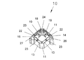
図1は、カラー形である一体形の接続エレメントを、差込領域が見えるように示した等尺図である。接続エレメント1は、正方形であるカラー形のボディ10として成形されており、2つの相互に対向するコーナ領域14,16にそれぞれ、カラー11に対して垂直に入れられたノッチ15,17が設けられている。
FIG. 1 is an isometric view showing an integral connection element of a collar shape so that the insertion area can be seen. The connecting
ボディ10全体には、導電性コーティングが被覆されている。
The
ノッチ15,17はたとえば、カラー厚さに相応する開口幅を有し、同図では、カラー全体の高さの約半分の高さに相応する深さを有する。
The
ボディ10には、両ノッチ15,17によって囲まれたコーナ領域18において、絶縁性材料から成形されたコンタクトホルダ30が挿入されている。このコンタクトホルダ30は、ここではシングルコンタクトとして形成されている信号コンタクト40を収容するように設けられている。コンタクトホルダ30は差込側に、ここでは3角形の吸着面31を有している。これはいわゆるピックアンドプレイス箇所として、接続エレメントがプリント基板に機械制御によって位置決めされるように形成されている。
A
カラー11は、両面で内側と外側とで包囲する傾斜部20,21を有する差込側カラー縁部12を備えている。この傾斜部20,21によって、2つの同一の接続エレメントを容易に相互にスライド挿入することができる。
The
コーナ領域14,16にはさらに、外側に向かって作用する整列エレメントが一体成形されており、これはスロット26およびばね27として形成されている。このばね27は、外側領域で先細りされて漏斗形に成形されることにより、複数の接続エレメントを整列する際に第一に、スロット‐ばねの組み合わせの比較的厚い中間領域が形状接続的な結合を成すまで、ばねがスロットに容易に挿入される。その際には、スロット26も同様に、外側領域が拡げられた漏斗形の長手形状を有することに留意すべきである。
The
図2は、接続エレメントの正方形のボディ10をはんだ側から見た図である。
FIG. 2 is a view of the
ここで重要なのはまず、コーナ領域18を形成する両カラー側11に設けられた2つのT形の切欠部19である。ここではコンタクトホルダ30は、相応に突起する係止軌道32によってスライド挿入されて保持される。
What is important here is firstly two T-
さらに、コーナ領域はスロット24を有し、このスロット24に、信号コンタクトに一体成形されたはんだ脚部42が挿入されることにより、プリント基板上のはんだパッドにはんだ付けされるように形成されている。
Further, the corner region has a
ここでは、はんだ側のカラー縁部13に2つの固定ピン22が一体成形されており、これらは、はんだ付け過程ではんだ手段が、カラー縁部に設けられた穿孔23内にキャピラリ力によって上昇し、該カラー縁部と該穿孔23とを最終的に固定完了するまで、プリント基板において極性付けおよび保持のために使用される。
Here, two fixing
図3a,3b,3cは、信号コンタクト40が挿入されるコンタクトホルダ30を複数の表現で示す。図3aおよび3bには垂直ポジションが示されており、図3cには逆のポジションが示されている。
3a, 3b, 3c show in multiple expressions the
輪郭はコーナ領域18への挿入に相応して、3角形の脚部36として、ボディ10の壁高さに相応して最大で内側の傾斜部分20にまで到達する高さで成形されている。上側が平滑なこの3角形は、プリント基板上に接続エレメント全体を機械制御で位置決めするための吸着領域31が設けられている。
The contour is shaped as a
中央には柱状構造があるのが見て取れる。両柱間の切欠部のここでは上側にアパーチャ33が形成されており、下側領域には凹入部34が形成されており、脚部にはポケット35が形成されている。突出している垂直な係止軌道32によって、コンタクトホルダがボディ10のT字形の切欠部19に固定されるのが保証される。
It can be seen that there is a columnar structure in the center. Here, an
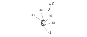
最後に、図4a、4bに示された信号コンタクト40は、外側に向かって撓曲されたコンタクト領域41と扁平なはんだ脚部42とを有するU字形状を有する。
Finally, the
上側の脚部端部と下側の脚部端部と撓曲されたコンタクト領域の下方である3つの位置にそれぞれ3面で露出されている係止づめ43が外側に撓曲されている。これらの係止づめによって、信号コンタクトはアパーチャ33と凹入部34とポケット35とにロックされる。
Locking
図5に、接続エレメント1の1つの変形形態1′が示されている。この変形形態1′では、内壁と、異なる角度で形成された差込側のカラー縁部12の内部および外部とにのみ導電性コーティングが設けられており、これによって、完全に差し込まれたときに最大限の高周波シールド作用が実現されるようにされている。さらにここでは、信号コンタクト40に対する絶縁性のコンタクトホルダ30がボディに直接成形されている。この導電性コーティングは、特に示されていない。
FIG. 5 shows a
図6aに2つの接続エレメント1または1′が示されている。これは、それぞれプリント基板3,5に取り付けられて、相互にコンタクトする。ここでは、プリント基板5を有する上側の接続エレメントが180°回転されている。カラー11に対角線上に形成されたノッチ15,17によって、両ボディを僅かにずらして、相互に完全に差し込むことができる。その際にはまず、2つの内側にある信号コンタクトがしばらくしてから相互にコンタクトするまで、カラー壁のシールドコーティングがコンタクトする。
In FIG. 6a two connecting
最後に図6bに、プリント基板の異なる間隔と同義である異なる高さが、接続エレメントの異なる高さ構成によって比較的容易に実現できるのが示されている。ここではまず、約6〜30mmのプリント基板間隔が設けられている。ボディの中央領域に対してのみ延長部が設けられており、差込側カラー縁部とはんだ側カラー縁部との双方の構成は変化されないまま維持される。ここでは、信号コンタクトの適切な延長部が設けられているので、コンタクトホルダの延長も必要である。 Finally, FIG. 6b shows that different heights, which are synonymous with different spacings of the printed circuit boards, can be realized relatively easily with different height configurations of the connecting elements. Here, first, a printed circuit board interval of about 6 to 30 mm is provided. An extension is provided only for the central region of the body, and the configuration of both the insertion side collar edge and the solder side collar edge is maintained unchanged. Here, since an appropriate extension of the signal contact is provided, the contact holder must also be extended.
図7に2つの差し込まれた接続エレメント1が示されている。ここでは、上側のプリント基板は取り外されている。
In FIG. 7, two plugged
ここでは、両信号コンタクト40がコンタクトされているのが明確に示されており、これらは、外側に向かって撓曲されたコンタクト領域41によって、対角線上の力成分を発生する。これによって、両接続エレメントのボディ10は常に、対向するコーナ領域に押し込まれ、接地信号を伝送するためのコーティングも確実にコンタクトされるのが保証される。
Here, it is clearly shown that both
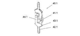
図8に、上記の接続エレメント1の1つの変形形態が示されている。この変形形態では多重コンタクト40.1が示されており、これはボディ10内部においてコンタクトホルダ30内に配置されている。図9aに示された多重コンタクト40.1は、2つの相互に接続されたコンタクト脚部を有する雌雄両性のコンタクトエレメントとして形成されている。これらのコンタクト脚部のうち1つは、直線上の扁平なコンタクト脚部44.1であり、他方はたとえばS字形のコンタクト脚部41.1であり、これははんだ脚部42.1と組み合わされて、プリント基板の適切な穿孔に挿入されるように形成されている。
FIG. 8 shows a variant of the
こうするためには、図9bに示された多重コンタクトの表面実装型も提供される。 To do this, the multi-contact surface-mount version shown in FIG. 9b is also provided.
最後に図10に、接続エレメント1の1つの変形形態がプリント基板の部分断片3とともに示されている。この変形形態では、接続エレメントは楕円形状のボディ10.1を有し、このボディ10.1内に信号コンタクト40はコンタクトホルダ30によって保持される。
Finally, FIG. 10 shows a variant of the connecting
1,1′ 接続エレメント、変形形態
3 プリント基板1
5 プリント基板2
10,10′ ボディ 10.1 楕円形のボディ
11 カラー
12 カラー縁部、差込側
13 カラー縁部、はんだ側
14 第1のコーナ領域A
15 ノッチA
16 第2のコーナ領域B
17 ノッチB
18 第3のコーナ領域C
19 コンタクトホルダに対する切欠部、T字形
20 傾斜部分、内側
21 傾斜部分、外側
22 固定ピン
23 穿孔
24 信号コンタクトに対するスロット形の切欠部
25 整列エレメント
26 スロット、直線状
27 ばね、漏斗形
28 (はんだパッド)
29 (はんだパッドに対する切欠部)
30 コンタクトホルダ 30.1 コンタクトホルダ、多重コンタクト
31 吸着領域、ピックアンドプレイス
32 係止軌道、突出
33 信号コンタクトに対するアパーチャ、上側
34 凹入部
35 信号コンタクトに対する切欠部、ポケット、下側
36 脚部
40 シングル信号コンタクト 40.1 多重コンタクト 40.2 SMDコンタクト
41 湾曲されたコンタクト領域 41.1 S字形のコンタクト脚部 41.2 S字形の脚部
42 はんだ脚部、扁平 42.1 はんだ脚部 42.2 SMDはんだ脚部
43 係止ラッチ 43.1 係止ラッチ 43.2 係止ラッチ
44.1 直線状のコンタクト脚部 44.2 直線状の脚部
1, 1 'connection element, modified
5 Printed circuit board 2
10, 10 'body 10.1
15 Notch A
16 Second corner area B
17 Notch B
18 Third corner area C
19 Notch for contact holder, T-shaped 20 Inclined portion, inside 21 Inclined portion, outside 22
29 (Notch to solder pad)
30 Contact Holder 30.1 Contact Holder,
Claims (1)
相互に係合されるように形成された表面実装可能な接続エレメント(1)を有し、
該接続エレメント(1)は差込側とはんだ側とを有する形式のものにおいて、
該接続エレメント(1)は、多角形の包囲壁状に形成されたカラー(11)を有するように形成された多面体形の対称的なボディ(10)を有し、
前記ボディ(10)全体に導電性コーティングが被覆されており、
前記カラー(11)の2つの対向するコーナ領域である第1のコーナ領域(14)および第2のコーナ領域(16)において前記カラー(11)にノッチ(15,17)が設けられており、
前記カラー(11)の内側に、両ノッチ(15,17)間の第3のコーナ領域(18)において、該カラー(11)の中心を向いている少なくとも1つの電気的な信号コンタクト(40)を保持するための、絶縁性材料から成形されたコンタクトホルダ(30)が次のように設けられており、すなわち、前記2つのプリント基板(3,5)間で前記接続エレメント(1)の電気的なコンタクトが行われたときに相手側の接続エレメント(1)のコンタクトホルダ(30)を収容するための空間が、各接続エレメント(1)の前記カラー(11)の前記第3のコーナ領域(18)に対向する第4のコーナ領域と該コンタクトホルダ(30)との間に形成されるように設けられており、
前記信号コンタクト(40)は、前記導電性コーティングによって被覆されたボディ(10)から該絶縁性材料によって電気的に絶縁され、
前記信号コンタクト(40)は前記第4のコーナ領域を向くように前記コンタクトホルダ(30)によって保持されることにより、前記2つの接続エレメント(1)の電気的コンタクト時に該第4のコーナ領域と該コンタクトホルダ(30)との間の空間に収容される相手側の接続エレメント(1)のコンタクトホルダ(30)によって保持された相手側の信号コンタクト(40)と対向して接触するようにされ、
前記ボディ(10)を前記プリント基板(3,5)に取り付けるために、前記コンタクトホルダ(30)に、機械制御による装着のための吸着面(31)が設けられており、
各接続エレメント(1)は相手側の接続エレメント(1)とそれ自体で、前記ノッチで相互に差込可能に形成されており、
各接続エレメント(1)が相手側の接続エレメント(1)と係合されたとき、両接続エレメント(1)のボディの導電性コーティングが相互にコンタクトし、該接続エレメント内の、相互に接続された両方の信号コンタクト(40)が、前記導電性コーティングによって被覆されたボディ(10)によって囲まれることによってシールドされ、該信号コンタクト(40)で信号を、ノイズに対して強く高周波信号伝送することができることを特徴とする、プリント基板カード差込接続部。 A printed circuit board card plug-in connection for making electrical contact between two parallel and mutually spaced apart printed circuit boards (3, 5),
Having surface mountable connection elements (1) formed to be engaged with each other;
The connecting element (1) has a plug side and a solder side,
The connecting element (1) has a polyhedral symmetrical body (10) formed to have a collar (11) formed in the shape of a polygonal enclosing wall ,
The entire body (10) is covered with a conductive coating,
The collar (11 ) is provided with notches (15, 17) in the first corner area (14) and the second corner area (16), which are two opposing corner areas of the collar (11),
Inside the collar (11), in a third corner region between the two notches (15, 17) (18), at least one electrical signal contacts facing the center of the collar (11) (40) A contact holder (30) molded from an insulating material is provided as follows, that is, the electric power of the connection element (1) between the two printed circuit boards (3, 5). A space for accommodating the contact holder (30) of the mating connection element (1) when a typical contact is made is the third corner area of the collar (11) of each connection element (1) (18) is provided so as to be formed between the fourth corner region facing the contact holder (30),
The signal contact (40) is electrically insulated from the body (10) covered by the conductive coating by the insulating material;
The signal contact (40) is held by the contact holder (30) so as to face the fourth corner region, so that when the two connecting elements (1) are in electrical contact with the fourth corner region, It is made to contact the mating signal contact (40) held by the contact holder (30) of the mating connection element (1) accommodated in the space between the contact holder (30). ,
In order to attach the body (10) to the printed circuit board (3, 5), the contact holder (30) is provided with a suction surface (31) for attachment by machine control,
Each connecting element (1) and itself other side of the connection element (1), which is pluggable formed with each other in the notch,
When each connecting element (1) is engaged with the mating connecting element (1) , the conductive coatings on the bodies of both connecting elements (1) contact each other and are connected to each other in the connecting element. Both signal contacts (40) are shielded by being surrounded by a body (10) covered by the conductive coating, and the signal contacts (40) transmit signals at high frequencies against noise. A printed circuit board card insertion connection part, characterized in that
Applications Claiming Priority (2)
| Application Number | Priority Date | Filing Date | Title |
|---|---|---|---|
| DE102007006204A DE102007006204B3 (en) | 2007-02-08 | 2007-02-08 | Conductor card pad connection for printed circuit board, has single-piece, surface-mounted connection unit formed as quadratic, multi-sided symmetrical base body, and notches provided between two edge areas |
| DE102007006204.6 | 2007-02-08 |
Publications (2)
| Publication Number | Publication Date |
|---|---|
| JP2008198606A JP2008198606A (en) | 2008-08-28 |
| JP4709863B2 true JP4709863B2 (en) | 2011-06-29 |
Family
ID=39185274
Family Applications (1)
| Application Number | Title | Priority Date | Filing Date |
|---|---|---|---|
| JP2008028931A Expired - Fee Related JP4709863B2 (en) | 2007-02-08 | 2008-02-08 | Printed circuit board card insertion connection for two parallel printed circuit boards |
Country Status (7)
| Country | Link |
|---|---|
| US (1) | US7513780B2 (en) |
| EP (1) | EP1973201B1 (en) |
| JP (1) | JP4709863B2 (en) |
| CN (1) | CN101242039B (en) |
| AT (1) | ATE518278T1 (en) |
| DE (1) | DE102007006204B3 (en) |
| ES (1) | ES2369025T3 (en) |
Families Citing this family (7)
| Publication number | Priority date | Publication date | Assignee | Title |
|---|---|---|---|---|
| CH701206A2 (en) * | 2009-06-02 | 2010-12-15 | Huber+Suhner Ag | Printed circuit board assembly. |
| WO2011091691A1 (en) | 2010-01-29 | 2011-08-04 | 华为技术有限公司 | Electromagnetic shielding method and device |
| CN202004200U (en) * | 2011-01-06 | 2011-10-05 | 富士康(昆山)电脑接插件有限公司 | Electric connector assembly |
| DE102011055750B3 (en) * | 2011-11-28 | 2013-02-14 | Harting Kgaa | Insulator of a connector |
| US9614334B2 (en) * | 2014-10-31 | 2017-04-04 | Microsoft Technology Licensing, Llc | Hermaphroditic electrical connector |
| CN105514728A (en) * | 2016-01-05 | 2016-04-20 | 陈烁 | Connecting plug |
| BE1026214B1 (en) | 2018-04-17 | 2019-11-19 | Phoenix Contact Gmbh & Co. Kg | Connector part with hermaphroditic contact elements |
Citations (6)
| Publication number | Priority date | Publication date | Assignee | Title |
|---|---|---|---|---|
| JPH0499369U (en) * | 1991-01-11 | 1992-08-27 | ||
| JPH0517946U (en) * | 1991-08-09 | 1993-03-05 | 日本航空電子工業株式会社 | connector |
| JPH06510158A (en) * | 1991-08-08 | 1994-11-10 | ロビンソン・ヌジエント・インコーポレーテツド | Inter-board wiring |
| JPH07161415A (en) * | 1993-12-02 | 1995-06-23 | Amp Japan Ltd | Electric connector and electric contact using this connector |
| JPH07326430A (en) * | 1994-05-31 | 1995-12-12 | Amp Japan Ltd | Electric connector and contact for use therewith |
| JP2006066384A (en) * | 2004-07-27 | 2006-03-09 | Hosiden Corp | Coaxial connector for board-to-board connection |
Family Cites Families (8)
| Publication number | Priority date | Publication date | Assignee | Title |
|---|---|---|---|---|
| US5156553A (en) * | 1990-05-29 | 1992-10-20 | Kel Corporation | Connector assembly for film circuitry |
| US5055054A (en) * | 1990-06-05 | 1991-10-08 | E. I. Du Pont De Nemours And Company | High density connector |
| FR2677816B1 (en) * | 1991-06-17 | 1995-04-28 | Radiall Sa | COAXIAL CONNECTOR FOR THE CONNECTION OF A COAXIAL CABLE TO A PRINTED ELECTRONIC CIRCUIT BOARD. |
| US5181855A (en) * | 1991-10-03 | 1993-01-26 | Itt Corporation | Simplified contact connector system |
| US5498167A (en) * | 1994-04-13 | 1996-03-12 | Molex Incorporated | Board to board electrical connectors |
| US6752637B2 (en) * | 2001-02-06 | 2004-06-22 | Ford Global Technologies, Llc | Flexible circuit relay |
| CN2772061Y (en) * | 2005-02-04 | 2006-04-12 | 上海莫仕连接器有限公司 | Electrical connector assembly |
| TWM284091U (en) * | 2005-04-21 | 2005-12-21 | Molex Taiwan Ltd | Electrical connector |
-
2007
- 2007-02-08 DE DE102007006204A patent/DE102007006204B3/en not_active Expired - Fee Related
-
2008
- 2008-01-24 US US12/019,580 patent/US7513780B2/en active Active
- 2008-02-02 EP EP08001989A patent/EP1973201B1/en active Active
- 2008-02-02 ES ES08001989T patent/ES2369025T3/en active Active
- 2008-02-02 AT AT08001989T patent/ATE518278T1/en active
- 2008-02-04 CN CN2008100048378A patent/CN101242039B/en active Active
- 2008-02-08 JP JP2008028931A patent/JP4709863B2/en not_active Expired - Fee Related
Patent Citations (6)
| Publication number | Priority date | Publication date | Assignee | Title |
|---|---|---|---|---|
| JPH0499369U (en) * | 1991-01-11 | 1992-08-27 | ||
| JPH06510158A (en) * | 1991-08-08 | 1994-11-10 | ロビンソン・ヌジエント・インコーポレーテツド | Inter-board wiring |
| JPH0517946U (en) * | 1991-08-09 | 1993-03-05 | 日本航空電子工業株式会社 | connector |
| JPH07161415A (en) * | 1993-12-02 | 1995-06-23 | Amp Japan Ltd | Electric connector and electric contact using this connector |
| JPH07326430A (en) * | 1994-05-31 | 1995-12-12 | Amp Japan Ltd | Electric connector and contact for use therewith |
| JP2006066384A (en) * | 2004-07-27 | 2006-03-09 | Hosiden Corp | Coaxial connector for board-to-board connection |
Also Published As
| Publication number | Publication date |
|---|---|
| EP1973201A2 (en) | 2008-09-24 |
| ATE518278T1 (en) | 2011-08-15 |
| EP1973201B1 (en) | 2011-07-27 |
| ES2369025T3 (en) | 2011-11-24 |
| CN101242039B (en) | 2010-12-15 |
| JP2008198606A (en) | 2008-08-28 |
| US7513780B2 (en) | 2009-04-07 |
| DE102007006204B3 (en) | 2008-04-17 |
| US20080194125A1 (en) | 2008-08-14 |
| CN101242039A (en) | 2008-08-13 |
| EP1973201A3 (en) | 2010-06-02 |
Similar Documents
| Publication | Publication Date | Title |
|---|---|---|
| CN110800169B (en) | Electrical connector device | |
| JP4709863B2 (en) | Printed circuit board card insertion connection for two parallel printed circuit boards | |
| CN108258484B (en) | Electric connector and combination thereof | |
| EP2636102B1 (en) | Contact element for plug-in connector socket | |
| US7074085B2 (en) | Shielded electrical connector assembly | |
| TWI758340B (en) | Receptacle connector | |
| JP4578522B2 (en) | Low inductance shield connector | |
| US7320605B2 (en) | Board-to-board connector with improved terminal contacts | |
| JP5178847B2 (en) | RF plug connector, RF receptacle connector, and RF connector | |
| US20180151985A1 (en) | Electrical connector having shielding plate retained tightly thereto | |
| CN112640228B (en) | Coaxial connector device | |
| KR960706701A (en) | CONNECTOR FOR HIGH DENSITY ELECTRONIC ASSEMBLIES | |
| JP2008123873A (en) | Electric connector | |
| US7494378B1 (en) | Board-to-board connector assembly | |
| US7553168B2 (en) | Electrical connector assembly | |
| JP2015520499A (en) | Plug-in connector insulation | |
| JP5445622B2 (en) | Antenna connection switching device | |
| JP2005251746A (en) | Plug socket connector of very small size | |
| KR102277740B1 (en) | Printed Circuit Board Connectors with Shielding Elements | |
| JP2006521001A (en) | Audio jack connector | |
| TWI673920B (en) | Electrical connector assembly | |
| CN111786200A (en) | Multi-polar substrate electric connector | |
| TWM584045U (en) | Grounding structure of electrical connector | |
| EP0954058A2 (en) | Flexible circuit electrical connector assembly | |
| CN215377772U (en) | Electrical connector |
Legal Events
| Date | Code | Title | Description |
|---|---|---|---|
| A131 | Notification of reasons for refusal |
Free format text: JAPANESE INTERMEDIATE CODE: A131 Effective date: 20100401 |
|
| A601 | Written request for extension of time |
Free format text: JAPANESE INTERMEDIATE CODE: A601 Effective date: 20100629 |
|
| A602 | Written permission of extension of time |
Free format text: JAPANESE INTERMEDIATE CODE: A602 Effective date: 20100702 |
|
| A601 | Written request for extension of time |
Free format text: JAPANESE INTERMEDIATE CODE: A601 Effective date: 20100802 |
|
| A602 | Written permission of extension of time |
Free format text: JAPANESE INTERMEDIATE CODE: A602 Effective date: 20100805 |
|
| A601 | Written request for extension of time |
Free format text: JAPANESE INTERMEDIATE CODE: A601 Effective date: 20100901 |
|
| A602 | Written permission of extension of time |
Free format text: JAPANESE INTERMEDIATE CODE: A602 Effective date: 20100906 |
|
| A521 | Request for written amendment filed |
Free format text: JAPANESE INTERMEDIATE CODE: A523 Effective date: 20100922 |
|
| A131 | Notification of reasons for refusal |
Free format text: JAPANESE INTERMEDIATE CODE: A131 Effective date: 20101022 |
|
| RD04 | Notification of resignation of power of attorney |
Free format text: JAPANESE INTERMEDIATE CODE: A7424 Effective date: 20101227 |
|
| RD04 | Notification of resignation of power of attorney |
Free format text: JAPANESE INTERMEDIATE CODE: A7424 Effective date: 20101228 |
|
| A521 | Request for written amendment filed |
Free format text: JAPANESE INTERMEDIATE CODE: A523 Effective date: 20110124 |
|
| A01 | Written decision to grant a patent or to grant a registration (utility model) |
Free format text: JAPANESE INTERMEDIATE CODE: A01 Effective date: 20110218 |
|
| A61 | First payment of annual fees (during grant procedure) |
Free format text: JAPANESE INTERMEDIATE CODE: A61 Effective date: 20110318 |
|
| R250 | Receipt of annual fees |
Free format text: JAPANESE INTERMEDIATE CODE: R250 |
|
| R250 | Receipt of annual fees |
Free format text: JAPANESE INTERMEDIATE CODE: R250 |
|
| R250 | Receipt of annual fees |
Free format text: JAPANESE INTERMEDIATE CODE: R250 |
|
| R250 | Receipt of annual fees |
Free format text: JAPANESE INTERMEDIATE CODE: R250 |
|
| LAPS | Cancellation because of no payment of annual fees |