EP1970471A2 - Elektrode zur Elektrolyse und Elektrolyseeinheit - Google Patents
Elektrode zur Elektrolyse und Elektrolyseeinheit Download PDFInfo
- Publication number
- EP1970471A2 EP1970471A2 EP08003969A EP08003969A EP1970471A2 EP 1970471 A2 EP1970471 A2 EP 1970471A2 EP 08003969 A EP08003969 A EP 08003969A EP 08003969 A EP08003969 A EP 08003969A EP 1970471 A2 EP1970471 A2 EP 1970471A2
- Authority
- EP
- European Patent Office
- Prior art keywords
- electrode
- electrolysis
- surface layer
- substrate
- ozone
- Prior art date
- Legal status (The legal status is an assumption and is not a legal conclusion. Google has not performed a legal analysis and makes no representation as to the accuracy of the status listed.)
- Withdrawn
Links
- 238000005868 electrolysis reaction Methods 0.000 title claims abstract description 144
- 239000002344 surface layer Substances 0.000 claims abstract description 149
- 239000000758 substrate Substances 0.000 claims abstract description 88
- BPUBBGLMJRNUCC-UHFFFAOYSA-N oxygen(2-);tantalum(5+) Chemical compound [O-2].[O-2].[O-2].[O-2].[O-2].[Ta+5].[Ta+5] BPUBBGLMJRNUCC-UHFFFAOYSA-N 0.000 claims abstract description 53
- 229910001936 tantalum oxide Inorganic materials 0.000 claims abstract description 48
- XLYOFNOQVPJJNP-UHFFFAOYSA-N water Substances O XLYOFNOQVPJJNP-UHFFFAOYSA-N 0.000 claims abstract description 40
- TWNQGVIAIRXVLR-UHFFFAOYSA-N oxo(oxoalumanyloxy)alumane Chemical compound O=[Al]O[Al]=O TWNQGVIAIRXVLR-UHFFFAOYSA-N 0.000 claims abstract description 33
- QGLKJKCYBOYXKC-UHFFFAOYSA-N nonaoxidotritungsten Chemical compound O=[W]1(=O)O[W](=O)(=O)O[W](=O)(=O)O1 QGLKJKCYBOYXKC-UHFFFAOYSA-N 0.000 claims abstract description 20
- 229910001930 tungsten oxide Inorganic materials 0.000 claims abstract description 20
- 239000012212 insulator Substances 0.000 claims abstract description 19
- 239000010410 layer Substances 0.000 claims description 92
- 229910052751 metal Inorganic materials 0.000 claims description 22
- 239000002184 metal Substances 0.000 claims description 22
- 229910044991 metal oxide Inorganic materials 0.000 claims description 16
- 150000004706 metal oxides Chemical class 0.000 claims description 16
- 238000005341 cation exchange Methods 0.000 claims description 10
- 230000035699 permeability Effects 0.000 claims description 7
- 239000002131 composite material Substances 0.000 claims description 4
- CBENFWSGALASAD-UHFFFAOYSA-N Ozone Chemical compound [O-][O+]=O CBENFWSGALASAD-UHFFFAOYSA-N 0.000 abstract description 98
- 239000008151 electrolyte solution Substances 0.000 abstract description 16
- 239000010409 thin film Substances 0.000 abstract description 9
- 238000000034 method Methods 0.000 description 72
- BASFCYQUMIYNBI-UHFFFAOYSA-N platinum Chemical group [Pt] BASFCYQUMIYNBI-UHFFFAOYSA-N 0.000 description 62
- 239000000463 material Substances 0.000 description 36
- 239000010408 film Substances 0.000 description 30
- 229910052697 platinum Inorganic materials 0.000 description 27
- GWEVSGVZZGPLCZ-UHFFFAOYSA-N Titan oxide Chemical compound O=[Ti]=O GWEVSGVZZGPLCZ-UHFFFAOYSA-N 0.000 description 25
- 238000002441 X-ray diffraction Methods 0.000 description 22
- OGIDPMRJRNCKJF-UHFFFAOYSA-N titanium oxide Inorganic materials [Ti]=O OGIDPMRJRNCKJF-UHFFFAOYSA-N 0.000 description 22
- 239000013078 crystal Substances 0.000 description 20
- 229910052782 aluminium Inorganic materials 0.000 description 19
- 238000006243 chemical reaction Methods 0.000 description 17
- 238000004544 sputter deposition Methods 0.000 description 16
- 238000002474 experimental method Methods 0.000 description 15
- 239000007789 gas Substances 0.000 description 15
- 238000004519 manufacturing process Methods 0.000 description 14
- 230000015572 biosynthetic process Effects 0.000 description 13
- 230000001590 oxidative effect Effects 0.000 description 13
- -1 RbOx Inorganic materials 0.000 description 12
- QVGXLLKOCUKJST-UHFFFAOYSA-N atomic oxygen Chemical compound [O] QVGXLLKOCUKJST-UHFFFAOYSA-N 0.000 description 12
- 238000001354 calcination Methods 0.000 description 12
- 229910052760 oxygen Inorganic materials 0.000 description 12
- 239000001301 oxygen Substances 0.000 description 12
- 239000000126 substance Substances 0.000 description 12
- 229910052715 tantalum Inorganic materials 0.000 description 12
- GUVRBAGPIYLISA-UHFFFAOYSA-N tantalum atom Chemical compound [Ta] GUVRBAGPIYLISA-UHFFFAOYSA-N 0.000 description 12
- XAGFODPZIPBFFR-UHFFFAOYSA-N aluminium Chemical compound [Al] XAGFODPZIPBFFR-UHFFFAOYSA-N 0.000 description 10
- 239000003792 electrolyte Substances 0.000 description 9
- 239000008399 tap water Substances 0.000 description 9
- 235000020679 tap water Nutrition 0.000 description 9
- 239000010936 titanium Substances 0.000 description 9
- 239000004020 conductor Substances 0.000 description 8
- 238000010586 diagram Methods 0.000 description 8
- 238000003411 electrode reaction Methods 0.000 description 7
- 239000000243 solution Substances 0.000 description 7
- XEKOWRVHYACXOJ-UHFFFAOYSA-N Ethyl acetate Chemical compound CCOC(C)=O XEKOWRVHYACXOJ-UHFFFAOYSA-N 0.000 description 6
- YADSGOSSYOOKMP-UHFFFAOYSA-N dioxolead Chemical compound O=[Pb]=O YADSGOSSYOOKMP-UHFFFAOYSA-N 0.000 description 6
- 229910052719 titanium Inorganic materials 0.000 description 6
- RTAQQCXQSZGOHL-UHFFFAOYSA-N Titanium Chemical compound [Ti] RTAQQCXQSZGOHL-UHFFFAOYSA-N 0.000 description 5
- 238000011156 evaluation Methods 0.000 description 5
- VSCWAEJMTAWNJL-UHFFFAOYSA-K aluminium trichloride Chemical compound Cl[Al](Cl)Cl VSCWAEJMTAWNJL-UHFFFAOYSA-K 0.000 description 4
- 150000001875 compounds Chemical class 0.000 description 4
- 125000000524 functional group Chemical group 0.000 description 4
- 239000012535 impurity Substances 0.000 description 4
- 239000002904 solvent Substances 0.000 description 4
- 230000005689 Fowler Nordheim tunneling Effects 0.000 description 3
- KDLHZDBZIXYQEI-UHFFFAOYSA-N Palladium Chemical compound [Pd] KDLHZDBZIXYQEI-UHFFFAOYSA-N 0.000 description 3
- 238000007254 oxidation reaction Methods 0.000 description 3
- 238000005546 reactive sputtering Methods 0.000 description 3
- 229910052709 silver Inorganic materials 0.000 description 3
- 239000004332 silver Substances 0.000 description 3
- 239000007787 solid Substances 0.000 description 3
- 238000002230 thermal chemical vapour deposition Methods 0.000 description 3
- ZNOKGRXACCSDPY-UHFFFAOYSA-N tungsten trioxide Chemical compound O=[W](=O)=O ZNOKGRXACCSDPY-UHFFFAOYSA-N 0.000 description 3
- KRHYYFGTRYWZRS-UHFFFAOYSA-N Fluorane Chemical compound F KRHYYFGTRYWZRS-UHFFFAOYSA-N 0.000 description 2
- 229920000557 Nafion® Polymers 0.000 description 2
- XUIMIQQOPSSXEZ-UHFFFAOYSA-N Silicon Chemical compound [Si] XUIMIQQOPSSXEZ-UHFFFAOYSA-N 0.000 description 2
- BQCADISMDOOEFD-UHFFFAOYSA-N Silver Chemical compound [Ag] BQCADISMDOOEFD-UHFFFAOYSA-N 0.000 description 2
- CECABOMBVQNBEC-UHFFFAOYSA-K aluminium iodide Chemical compound I[Al](I)I CECABOMBVQNBEC-UHFFFAOYSA-K 0.000 description 2
- 238000004458 analytical method Methods 0.000 description 2
- 239000007864 aqueous solution Substances 0.000 description 2
- 238000004140 cleaning Methods 0.000 description 2
- HTXDPTMKBJXEOW-UHFFFAOYSA-N dioxoiridium Chemical compound O=[Ir]=O HTXDPTMKBJXEOW-UHFFFAOYSA-N 0.000 description 2
- 230000007613 environmental effect Effects 0.000 description 2
- 239000010931 gold Substances 0.000 description 2
- 125000001475 halogen functional group Chemical group 0.000 description 2
- 238000007733 ion plating Methods 0.000 description 2
- 229910000457 iridium oxide Inorganic materials 0.000 description 2
- 239000010955 niobium Substances 0.000 description 2
- 230000003647 oxidation Effects 0.000 description 2
- JMOHEPRYPIIZQU-UHFFFAOYSA-N oxygen(2-);tantalum(2+) Chemical compound [O-2].[Ta+2] JMOHEPRYPIIZQU-UHFFFAOYSA-N 0.000 description 2
- 238000007747 plating Methods 0.000 description 2
- 239000010948 rhodium Substances 0.000 description 2
- 229910052710 silicon Inorganic materials 0.000 description 2
- 239000010703 silicon Substances 0.000 description 2
- PUGUQINMNYINPK-UHFFFAOYSA-N tert-butyl 4-(2-chloroacetyl)piperazine-1-carboxylate Chemical compound CC(C)(C)OC(=O)N1CCN(C(=O)CCl)CC1 PUGUQINMNYINPK-UHFFFAOYSA-N 0.000 description 2
- 231100000167 toxic agent Toxicity 0.000 description 2
- 239000003440 toxic substance Substances 0.000 description 2
- 238000004876 x-ray fluorescence Methods 0.000 description 2
- ZXEYZECDXFPJRJ-UHFFFAOYSA-N $l^{3}-silane;platinum Chemical compound [SiH3].[Pt] ZXEYZECDXFPJRJ-UHFFFAOYSA-N 0.000 description 1
- NNDLQUNWZOIESH-UHFFFAOYSA-N 8-hydroxy-7-[[7-[(8-hydroxy-5-sulfoquinoline-7-carbonyl)amino]-4-[3-[(8-hydroxy-5-sulfoquinoline-7-carbonyl)amino]propyl]heptyl]carbamoyl]quinoline-5-sulfonic acid Chemical compound C1=CC=NC2=C(O)C(C(=O)NCCCC(CCCNC(=O)C=3C(=C4N=CC=CC4=C(C=3)S(O)(=O)=O)O)CCCNC(=O)C3=C(C4=NC=CC=C4C(=C3)S(O)(=O)=O)O)=CC(S(O)(=O)=O)=C21 NNDLQUNWZOIESH-UHFFFAOYSA-N 0.000 description 1
- PNEYBMLMFCGWSK-UHFFFAOYSA-N Alumina Chemical compound [O-2].[O-2].[O-2].[Al+3].[Al+3] PNEYBMLMFCGWSK-UHFFFAOYSA-N 0.000 description 1
- 229910000873 Beta-alumina solid electrolyte Inorganic materials 0.000 description 1
- 229910016300 BiOx Inorganic materials 0.000 description 1
- ZOXJGFHDIHLPTG-UHFFFAOYSA-N Boron Chemical compound [B] ZOXJGFHDIHLPTG-UHFFFAOYSA-N 0.000 description 1
- WKBOTKDWSSQWDR-UHFFFAOYSA-N Bromine atom Chemical compound [Br] WKBOTKDWSSQWDR-UHFFFAOYSA-N 0.000 description 1
- OKTJSMMVPCPJKN-UHFFFAOYSA-N Carbon Chemical compound [C] OKTJSMMVPCPJKN-UHFFFAOYSA-N 0.000 description 1
- 229910003320 CeOx Inorganic materials 0.000 description 1
- VEXZGXHMUGYJMC-UHFFFAOYSA-M Chloride anion Chemical compound [Cl-] VEXZGXHMUGYJMC-UHFFFAOYSA-M 0.000 description 1
- 229910002451 CoOx Inorganic materials 0.000 description 1
- 229910019923 CrOx Inorganic materials 0.000 description 1
- 229910016553 CuOx Inorganic materials 0.000 description 1
- 229910015189 FeOx Inorganic materials 0.000 description 1
- 229910005535 GaOx Inorganic materials 0.000 description 1
- 229910002616 GeOx Inorganic materials 0.000 description 1
- 235000000177 Indigofera tinctoria Nutrition 0.000 description 1
- 229910017947 MgOx Inorganic materials 0.000 description 1
- 229910016978 MnOx Inorganic materials 0.000 description 1
- 229910015711 MoOx Inorganic materials 0.000 description 1
- 101100096038 Mus musculus Smox gene Proteins 0.000 description 1
- 229910005855 NiOx Inorganic materials 0.000 description 1
- 229910020669 PbOx Inorganic materials 0.000 description 1
- 229910002830 PrOx Inorganic materials 0.000 description 1
- KJTLSVCANCCWHF-UHFFFAOYSA-N Ruthenium Chemical compound [Ru] KJTLSVCANCCWHF-UHFFFAOYSA-N 0.000 description 1
- 229910018316 SbOx Inorganic materials 0.000 description 1
- VYPSYNLAJGMNEJ-UHFFFAOYSA-N Silicium dioxide Chemical compound O=[Si]=O VYPSYNLAJGMNEJ-UHFFFAOYSA-N 0.000 description 1
- 229910006854 SnOx Inorganic materials 0.000 description 1
- 229910002347 SrOx Inorganic materials 0.000 description 1
- NRTOMJZYCJJWKI-UHFFFAOYSA-N Titanium nitride Chemical compound [Ti]#N NRTOMJZYCJJWKI-UHFFFAOYSA-N 0.000 description 1
- 229910007667 ZnOx Inorganic materials 0.000 description 1
- 229910003134 ZrOx Inorganic materials 0.000 description 1
- 230000002411 adverse Effects 0.000 description 1
- 125000003172 aldehyde group Chemical group 0.000 description 1
- 125000003545 alkoxy group Chemical group 0.000 description 1
- 125000000217 alkyl group Chemical group 0.000 description 1
- 229910045601 alloy Inorganic materials 0.000 description 1
- 239000000956 alloy Substances 0.000 description 1
- 239000010405 anode material Substances 0.000 description 1
- 229910052796 boron Inorganic materials 0.000 description 1
- GDTBXPJZTBHREO-UHFFFAOYSA-N bromine Substances BrBr GDTBXPJZTBHREO-UHFFFAOYSA-N 0.000 description 1
- 229910052794 bromium Inorganic materials 0.000 description 1
- 229910052799 carbon Inorganic materials 0.000 description 1
- 125000003178 carboxy group Chemical group [H]OC(*)=O 0.000 description 1
- 239000012159 carrier gas Substances 0.000 description 1
- 239000003054 catalyst Substances 0.000 description 1
- 239000011248 coating agent Substances 0.000 description 1
- 238000000576 coating method Methods 0.000 description 1
- 229910003460 diamond Inorganic materials 0.000 description 1
- 239000010432 diamond Substances 0.000 description 1
- 239000003989 dielectric material Substances 0.000 description 1
- 230000000694 effects Effects 0.000 description 1
- 238000005516 engineering process Methods 0.000 description 1
- 230000008020 evaporation Effects 0.000 description 1
- 238000001704 evaporation Methods 0.000 description 1
- 235000013305 food Nutrition 0.000 description 1
- 239000011521 glass Substances 0.000 description 1
- PCHJSUWPFVWCPO-UHFFFAOYSA-N gold Chemical compound [Au] PCHJSUWPFVWCPO-UHFFFAOYSA-N 0.000 description 1
- 229910052737 gold Inorganic materials 0.000 description 1
- BHEPBYXIRTUNPN-UHFFFAOYSA-N hydridophosphorus(.) (triplet) Chemical compound [PH] BHEPBYXIRTUNPN-UHFFFAOYSA-N 0.000 description 1
- 125000002887 hydroxy group Chemical group [H]O* 0.000 description 1
- 229940097275 indigo Drugs 0.000 description 1
- COHYTHOBJLSHDF-UHFFFAOYSA-N indigo powder Natural products N1C2=CC=CC=C2C(=O)C1=C1C(=O)C2=CC=CC=C2N1 COHYTHOBJLSHDF-UHFFFAOYSA-N 0.000 description 1
- 229910052741 iridium Inorganic materials 0.000 description 1
- GKOZUEZYRPOHIO-UHFFFAOYSA-N iridium atom Chemical compound [Ir] GKOZUEZYRPOHIO-UHFFFAOYSA-N 0.000 description 1
- 239000005300 metallic glass Substances 0.000 description 1
- 150000002739 metals Chemical class 0.000 description 1
- 238000002156 mixing Methods 0.000 description 1
- 239000000203 mixture Substances 0.000 description 1
- 229910052758 niobium Inorganic materials 0.000 description 1
- GUCVJGMIXFAOAE-UHFFFAOYSA-N niobium atom Chemical compound [Nb] GUCVJGMIXFAOAE-UHFFFAOYSA-N 0.000 description 1
- 229910000510 noble metal Inorganic materials 0.000 description 1
- HBEQXAKJSGXAIQ-UHFFFAOYSA-N oxopalladium Chemical compound [Pd]=O HBEQXAKJSGXAIQ-UHFFFAOYSA-N 0.000 description 1
- 125000004430 oxygen atom Chemical group O* 0.000 description 1
- 229910052763 palladium Inorganic materials 0.000 description 1
- 229910003445 palladium oxide Inorganic materials 0.000 description 1
- 229910021339 platinum silicide Inorganic materials 0.000 description 1
- 229910052703 rhodium Inorganic materials 0.000 description 1
- MHOVAHRLVXNVSD-UHFFFAOYSA-N rhodium atom Chemical compound [Rh] MHOVAHRLVXNVSD-UHFFFAOYSA-N 0.000 description 1
- 229910052707 ruthenium Inorganic materials 0.000 description 1
- 229910001925 ruthenium oxide Inorganic materials 0.000 description 1
- WOCIAKWEIIZHES-UHFFFAOYSA-N ruthenium(iv) oxide Chemical compound O=[Ru]=O WOCIAKWEIIZHES-UHFFFAOYSA-N 0.000 description 1
- VSZWPYCFIRKVQL-UHFFFAOYSA-N selanylidenegallium;selenium Chemical compound [Se].[Se]=[Ga].[Se]=[Ga] VSZWPYCFIRKVQL-UHFFFAOYSA-N 0.000 description 1
- 239000004065 semiconductor Substances 0.000 description 1
- 239000010865 sewage Substances 0.000 description 1
- 229910052814 silicon oxide Inorganic materials 0.000 description 1
- 150000003378 silver Chemical class 0.000 description 1
- 230000001954 sterilising effect Effects 0.000 description 1
- 238000004659 sterilization and disinfection Methods 0.000 description 1
- 238000003756 stirring Methods 0.000 description 1
- 239000002887 superconductor Substances 0.000 description 1
- 150000003482 tantalum compounds Chemical class 0.000 description 1
- 231100000419 toxicity Toxicity 0.000 description 1
- 230000001988 toxicity Effects 0.000 description 1
- WFKWXMTUELFFGS-UHFFFAOYSA-N tungsten Chemical compound [W] WFKWXMTUELFFGS-UHFFFAOYSA-N 0.000 description 1
- 229910052721 tungsten Inorganic materials 0.000 description 1
- 239000010937 tungsten Substances 0.000 description 1
Images
Classifications
-
- C—CHEMISTRY; METALLURGY
- C25—ELECTROLYTIC OR ELECTROPHORETIC PROCESSES; APPARATUS THEREFOR
- C25B—ELECTROLYTIC OR ELECTROPHORETIC PROCESSES FOR THE PRODUCTION OF COMPOUNDS OR NON-METALS; APPARATUS THEREFOR
- C25B1/00—Electrolytic production of inorganic compounds or non-metals
- C25B1/01—Products
- C25B1/13—Ozone
-
- C—CHEMISTRY; METALLURGY
- C25—ELECTROLYTIC OR ELECTROPHORETIC PROCESSES; APPARATUS THEREFOR
- C25B—ELECTROLYTIC OR ELECTROPHORETIC PROCESSES FOR THE PRODUCTION OF COMPOUNDS OR NON-METALS; APPARATUS THEREFOR
- C25B11/00—Electrodes; Manufacture thereof not otherwise provided for
- C25B11/04—Electrodes; Manufacture thereof not otherwise provided for characterised by the material
- C25B11/051—Electrodes formed of electrocatalysts on a substrate or carrier
- C25B11/073—Electrodes formed of electrocatalysts on a substrate or carrier characterised by the electrocatalyst material
- C25B11/091—Electrodes formed of electrocatalysts on a substrate or carrier characterised by the electrocatalyst material consisting of at least one catalytic element and at least one catalytic compound; consisting of two or more catalytic elements or catalytic compounds
- C25B11/093—Electrodes formed of electrocatalysts on a substrate or carrier characterised by the electrocatalyst material consisting of at least one catalytic element and at least one catalytic compound; consisting of two or more catalytic elements or catalytic compounds at least one noble metal or noble metal oxide and at least one non-noble metal oxide
Definitions
- the present invention relates to an electrode for electrolysis for use in an industrial or household electrolysis process.
- ozone is a substance having a very strong oxidizing power, and it is expected that water in which ozone is dissolved, so-called ozone water is applied to a broad range of cleaning sterilization treatment of water and sewage, food and the like, and a cleaning treatment of a semiconductor device manufacturing process.
- methods for forming the ozone water there are known a method for dissolving, in water, ozone formed by irradiation with an ultraviolet ray or electric discharge, a method for forming ozone in water by electrolysis of the water, and the like.
- an ozone water forming device which includes ozone forming means for forming an ozone gas with an ultraviolet lamp and a tank to store water, whereby the formed ozone gas is supplied to the water in the tank to form the ozone water.
- Patent Document 2 an ozone water forming device is disclosed which mixes an ozone gas formed by a discharge type ozone gas forming device with water at a predetermined ratio by a mixing pump, in order to efficiently dissolve the ozone gas in the water.
- the ozone gas forming device an operation for dissolving the ozone gas in the water and the like are required, so that the device is liable to become complicated.
- the method is a method for dissolving the formed ozone gas in the water, and hence it has a problem that it is difficult to efficiently form the ozone water having a desired concentration.
- Patent Document 3 As a method for solving the above-mentioned problem, a method for forming ozone in water by the electrolysis of the water is disclosed.
- an electrode for forming ozone is used which is constituted of an electrode substrate material formed of a porous body or a mesh-like body, and an electrode catalyst including an oxide of a platinum group element or the like.
- Patent Document 4 model tap water as an electrolytic solution is electrolytically treated with an electrode for electrolysis including a surface layer made of a dielectric material such as tantalum oxide, to form ozone.
- the platinum group element is a standard anode material, and has a characteristic that the element is hardly dissolved in an aqueous solution which does not include any organic substance.
- the element as the electrode for forming ozone has a low ozone forming efficiency, and it is difficult to efficiently form the ozone water by an electrolysis process.
- the electrolysis for the ozone formation requires a high current density of 1 A/cm 2 or more, and an electrolyte needs to be set to a low temperature. This raises a problem that very high energy is consumed.
- platinum is expensive. When lead dioxide is used instead of platinum, there is a problem of toxicity.
- the present invention has been developed in order to solve a conventional technical problem, and an object thereof is to provide an electrode for electrolysis capable of efficiently forming ozone by electrolysis of water with a low current density.
- An electrode for electrolysis according to the invention of a first aspect comprises a substrate and a surface layer formed on the surface of the substrate, characterized in that the surface layer is an amorphous insulator.
- the electrode for electrolysis according to the invention of a second aspect is characterized in that in the above invention, the insulator is an oxide of a single metal or a composite metal oxide.
- the electrode for electrolysis according to the invention of a third aspect is characterized in that in the above inventions, the insulator is tantalum oxide or tungsten oxide.
- the electrode for electrolysis according to the invention of a fourth aspect is characterized in that in the inventions of the first and second aspects, the insulator is aluminum oxide.
- the electrode for electrolysis according to the invention of a fifth aspect is characterized in that in the above inventions, a thickness of the surface layer is in a range of 20 nm or more to 2000 nm or less.
- the electrode for electrolysis according to the invention of a sixth aspect is characterized in that in the above inventions, the substrate is provided with an intermediate layer positioned on an inner side of the surface layer and formed of a metal which is not easily oxidized on the surface of the substrate.
- An electrolysis unit of the invention of a seventh aspect is characterized in that an anode having water permeability is constituted of the electrode for electrolysis according to the above inventions, and the anode and a cathode having water permeability are arranged on both surfaces of a cation exchange film.
- the surface layer is the amorphous insulator, so that ozone can efficiently be formed by the electrolysis of an electrolytic solution with a low current density by use of the electrode as the anode.
- the temperature of the electrolytic solution does not have to be especially set to a low temperature, and the high current density is not required, so that power consumption required for the ozone formation can be reduced.
- the insulator is the oxide of the single metal or the composite metal oxide.
- the insulator is tantalum oxide or tungsten oxide.
- the electrons move with a higher energy level, whereby an ozone forming efficiency for causing the ozone forming reaction can be raised.
- the insulator is aluminum oxide, so that the electrode for electrolysis according to the above inventions can be made of a comparatively inexpensive material, and production cost can be reduced. Moreover, any toxic substance such as lead dioxide is not used, whereby an environmental load can be reduced.
- the thickness of the surface layer is in a range of 20 nm or more to 2000 nm or less, so that the surface layer can be made of a thin film, and the electrons can move in the electrode via impurities of the surface layer or Fowler-Nordheim tunneling. Therefore, owing to an electrode reaction in the anode, the empty level around the bottom of the conduction band at the energy level higher than Fermi level as much as about the half of the band gap can receive the electrons from the electrolyte, and the movement of the electrons is caused with the higher energy level, whereby the electrolysis can be performed with the low current density, and ozone can efficiently be formed.
- the substrate is provided with the intermediate layer positioned on the inner side of the surface layer and formed of the metal which is not easily oxidized on the surface of the substrate. Therefore, the electrode reaction can be caused with the high energy level in the surface of the surface layer. In consequence, ozone can efficiently be formed with a lower current density.
- the intermediate layer is formed of the metal which is not easily oxidized on the surface of the substrate. Therefore, when the electrolysis is performed with the electrode, it is possible to avoid a disadvantage that the substrate surface is oxidized and non-conducted. In consequence, durability of the electrode can be improved. As compared with the whole substrate is made of the material constituting the intermediate layer, the production cost can be reduced. Even in such a case, ozone can similarly efficiently be formed.
- the anode having the water permeability is constituted of the electrode for electrolysis according to the above inventions, and the anode and the cathode having the water permeability are arranged on both the surfaces of the cation exchange film. Therefore, protons move in the cation exchange film, whereby even when the electrolytic solution is pure water, ozone can efficiently be formed.
- FIG. 1 is a cross sectional view of an electrode 1 for electrolysis of the present invention.
- the electrode 1 for electrolysis is constituted of a substrate 2, a close contact layer 3 formed on the surface of the substrate 2, an intermediate layer 4 formed on the surface of the close contact layer 3, and a surface layer 5 formed on the surface of the intermediate layer 4.
- the substrate 2 is provided with a titanium plate 6 as an electric conductor, and conduction can be realized between the titanium plate 6 and the intermediate layer 4 via a silver paste 7 as a conductive material.
- this silver paste 7 and the titanium plate 6 are coated with a seal material 8, and this does not contribute to electrolysis. It is to be noted that a way to realize the conduction is not limited to this example.
- the substrate 2 is made of a conductive material of, for example, platinum (Pt), a valve metal such as titanium (Ti), tantalum (Ta), zirconium (Zr) or niobium (Nb), an alloy of two or more of these valve metals, silicon (Si) or the like.
- a valve metal such as titanium (Ti), tantalum (Ta), zirconium (Zr) or niobium (Nb), an alloy of two or more of these valve metals, silicon (Si) or the like.
- Si having the surface thereof treated so as to be flat is used in the substrate 2 for use in the present embodiment.
- the close contact layer 3 is formed on the surface of the substrate 2 so as to improve a close contact property between the substrate 2 and the intermediate layer 4 formed of, for example, platinum on the surface of the close contact layer 3, and the close contact layer is made of titanium oxide, titanium nitride or the like. It is to be noted that in the present embodiment, titanium oxide is used.
- the intermediate layer 4 is made of a metal which is not easily oxidized, for example, platinum or gold (Au), a conductive metal oxide such as iridium oxide, palladium oxide or ruthenium oxide, or an oxide superconductor.
- the intermediate layer is made of a metal which is oxidized but has conductivity, for example, ruthenium (Ru), rhodium (Rh), palladium (Pd), iridium (Ir) or silver (Ag) included in platinum group elements.
- the metal oxide is not limited to the oxide beforehand constituting the intermediate layer 4, and may include a metal oxide obtained by electrolytic oxidization.
- the intermediate layer 4 is made of the metal oxide having the conductivity, for example, iridium oxide or the like, the conductor is adversely affected by oxygen atoms constituting the metal oxide. Therefore, it is preferable that the intermediate layer 4 is made of the metal which is not easily oxidized. In the present embodiment, the intermediate layer 4 is made of platinum.
- the substrate 2 is made of platinum, needless to say, the surface of the substrate 2 is also made of platinum, so that the intermediate layer 4 does not have to be especially constituted.
- the substrate 2 is made of platinum in this manner, steep rise of cost is incurred. Therefore, it is industrially preferable that the substrate 2 is made of an inexpensive material, and the intermediate layer 4 made of a noble metal or the like is formed on the surface of the substrate 2.
- the substrate 2 is made of a substance which does not have any conductivity, for example, a glass plate and at least a contact surface between the substrate 2 and the surface layer 5 described later is coated with a material having the conductivity. This can also suppress steep rise of cost required for the material for use in constituting the substrate 2.
- the surface layer 5 is an amorphous (an infinite form, non-crystalline) insulator provided together with the intermediate layer 4 so as to coat the intermediate layer 4.
- the insulator is made of tantalum oxide (TaOx), tungsten oxide (WOx) or aluminum oxide (AlOx) in the form of a layer on the surface of the substrate 2.
- This surface layer 5 is formed into a thin film having a predetermined thickness above 0 to 1 mm or less, preferably 20 nm or 2000 nm in the present embodiment.
- examples of the insulator include amorphous tantalum oxide, tungsten oxide and aluminum oxide, but the insulator is not limited to these examples, and an amorphous oxide of a single metal as an insulator may be used.
- the oxide include TiOx, NbOx, HfOx, NaOx, MgOx, KOx, CaOx, ScOx, VOx, CrOx, MnOx, FeOx, CoOx, NiOx, CuOx, ZnOx, GaOx, RbOx, SrOx, YOx, ZrOx, MoOx, InOx, SnOx, SbOx, CsOx, BaOx, LaOx, CeOx, PrOx, NdOx, PmOx, SmOx, EuOx, GdOx, TbOx, DyOx, HoOx, ErOx, TmOx, YbOx, LuOx, PbOx and BiOx.
- an amorphous composite metal oxide as an insulator, SiOx, GeOx or the like may be used.
- Si silicon constituting a substrate 2 is pretreated in step S1.
- phosphorous (P), boron (B) and the like are introduced as impurities into Si to improve the conductivity.
- Si having a very flat surface is used. It is to be noted that in the present example, Si is used as the substrate 2, but a conductive material may be used.
- the substrate 2 of Si is treated with 5% of hydrofluoric acid to remove a native oxide film formed on the surface of the substrate 2.
- the surface of the substrate 2 is further flattened. It is to be noted that the pretreatment does not have to be performed.
- the surface of the substrate 2 is rinsed with pure water, and then in step S2, the substrate is introduced into a chamber of an existing sputtering system to form a film thereon.
- a close contact layer 3 for improving a close contact property of an intermediate layer 4 as described above is formed on the surface of the substrate 2.
- the close contact layer 3 is formed on the substrate 2 by a reactive sputtering process.
- the close contact layer 3 is made of titanium oxide, so that the film is formed at room temperature for ten minutes on conditions that Ti is used as a first target, a supply power is 6.17 W/cm 2 , an oxygen partial pressure is 52% (Ar:O 2 24:26) and a film forming pressure is 0.6 Pa.
- the close contact layer 23 of titanium oxide having a thickness of about 50 nm is formed on the surface of the substrate 2.
- the reactive sputtering process is used, but the present invention is not limited to this example.
- a sputtering process, a CVD process, an ion plating process, a plating process, or a combination of one of these processes and thermal oxidation may be used.
- the intermediate layer 4 is formed on the surface of the substrate 2 provided with the close contact layer 3.
- the intermediate layer 4 is formed on the surface of the substrate 2 by a sputtering process.
- the intermediate layer 4 is made of platinum, so that the film is formed at room temperature for about one minute and eleven seconds on conditions that Pt (80 mm ⁇ ) is used as a first target, a supply power is 4.63 W/cm 2 , and an Ar gas pressure is 0.7 Pa.
- the intermediate layer 4 having a thickness of about 200 nm is formed on the surface of the substrate 2 provided with the close contact layer 3.
- the sputtering process is used, but the present invention is not limited to this example.
- a CVD process, an evaporation process, an ion plating process, a plating process or the like may be used.
- a surface layer 5 is formed on the surface of the substrate 2 provided with the intermediate layer 4.
- the surface layer 5 is formed using a spin coat process, so that the surface of the substrate 2 provided with the intermediate layer 4 is coated with an organic aluminum compound solution as a surface layer constituting material.
- the surface layer 5 is made of aluminum oxide, so that an organic aluminum compound is used in which a functional group such as a hydroxyl group, an aldehyde group, an alkyl group, a carboxyl group or an alkoxyl group is coordinated in aluminum having a coordination number of 3.
- aluminum in this organic aluminum compound solution is in a range of about 0.4 wt% to 3 wt%.
- the organic aluminum compound solution is used as the surface layer constituting material, but the present invention is not limited to this example.
- An aluminum-containing compound from which a substance other than aluminum can be removed by calcinating, for example, aluminum chloride, aluminum bromide, aluminum iodide or the like may be used.
- step S4 the surface constituting material is dripped on the surface of the substrate 2 provided with an intermediate layer 4 to form a thin film by a spin coat process.
- conditions of the spin coat process are set to five seconds at 1000 rpm, 15 seconds at 3000 rpm.
- the surface of the substrate is dried in an environment at room temperature and then 200°C for ten minutes (step S5).
- a surface layer 5 is formed of the surface layer constituting material including the aluminum compound on the surface of the intermediate layer 4 of the substrate 2.
- step S6 the substrate 2 provided with the intermediate layer 4 and the surface layer 5 is calcinated (annealed) at 400°C to 900°C in a muffle furnace, at 600°C in atmospheric air for ten minutes to obtain the electrode 1 for electrolysis.
- the surface layer constituting material applied to the surface of the intermediate layer 4 is uniformly applied aluminum oxide.
- the present film forming operation is performed once, whereby the calcinated and formed surface layer 5 of aluminum oxide has a thickness of about 25 nm. It is to be noted that the film forming operation may be repeated as much as a plurality of times to set the thickness of the surface layer 5 to about 20 nm to 2000 nm.
- the surface layer 5 of the electrode 1 for electrolysis obtained as described above is all aluminum oxide. That is, the surface layer constituting material includes an aluminum-containing compound, for example, an organic aluminum compound in which a plurality of functional groups are coordinated in addition to aluminum. Alternatively, the material includes aluminum chloride, aluminum bromide, aluminum iodide or the like. The material is calcinated, whereby substances other than aluminum, that is, functional groups of organic substances, chloride, bromine and the like are removed. On the other hand, aluminum reacts with oxygen in the atmosphere to form aluminum oxide.
- an aluminum-containing compound for example, an organic aluminum compound in which a plurality of functional groups are coordinated in addition to aluminum.
- the material includes aluminum chloride, aluminum bromide, aluminum iodide or the like.
- the material is calcinated, whereby substances other than aluminum, that is, functional groups of organic substances, chloride, bromine and the like are removed.
- aluminum reacts with oxygen in the atmosphere to form aluminum oxide.
- FIG. 3 shows an X-ray diffraction pattern of the surface layer 5 of the electrode 1 for electrolysis obtained as described above.
- the electrode 1 for electrolysis is constituted on conditions that a calcinating temperature in constituting the surface layer 5 are 700°C, 750°C, 800°C, 850°C and 900°C.
- XRD X-ray diffraction
- the structure was observed using an X-ray diffraction apparatus (D8 Discover manufactured by Bruker AXS Co.).
- diffraction peaks (2 ⁇ ) shown in an X-ray diffraction pattern of the surface layer 5 of the electrode 1 for electrolysis obtained in the present example were about 36.1°, about 38° and about 39.6° regardless of the calcinating temperature at which the electrode 1 was constituted.
- crystal structure of aluminum oxide hexagonal system of ⁇ -alumina, ⁇ -alumina or the like is known, but diffraction peaks (2 ⁇ ) of 35.15°, 57.50° and 43.36° inherent in aluminum oxide (Al 2 O 3 ) were not present in any X-ray diffraction pattern of the surface layer 5 of the electrode 1 for electrolysis.
- aluminum oxide forming the surface layer 5 of the electrode 1 for electrolysis by the above method does not have any crystal structure, has an infinite form, and is, so-called amorphous. It is to be noted that in this case, the diffraction peak around 36.1° is a peak of titanium oxide (101) constituting a close contact layer 3, and the diffraction peak around 39.6° is a peak of platinum (111) constituting the intermediate layer 4.
- the surface layer 5 is formed of amorphous aluminum oxide by coating the surface of the substrate (the surface of the intermediate layer 4 in the present example) with a surface layer constituting material including an aluminum compound by a spin coat process to calcinate the material at a predetermined temperature, but the method constituting the surface layer 5 with amorphous aluminum oxide is not limited to this example.
- the surface layer 5 As another method, there is a method for forming the surface layer 5 by a thermal CVD process.
- the close contact layer 3 and the intermediate layer 4 are successively formed on the surface of the substrate 2 in the same manner as in the above example.
- the organic aluminum compound as the surface layer constituting material is vaporized, and guided to a reaction tube by use of an appropriate carrier gas to perform a chemical reaction on the surface of the substrate 2 heated to a high temperature of, for example, 500°C to 900°C, preferably 600°C to 800°C.
- an organic substance is removed from the surface of the substrate 2 heated to the high temperature, and only aluminum reacts with oxygen in the atmosphere to form aluminum oxide on the surface of the substrate 2.
- Aluminum oxide formed on the surface of the substrate 2 (in actual, the surface of the intermediate layer 4) constitutes an amorphous thin film (an aluminum oxide film).
- examples of the method for constituting the surface layer 5 of amorphous aluminum oxide include a dip process.
- the close contact layer 3 made of titanium oxide is formed on the surface of the substrate 2 made of Si. Therefore, platinum constituting the intermediate layer 4 is directly diffused in the substrate 2 to form platinum silicide, and it can be prevented that the substrate surface is oxidized and non-conducted during electrolysis.
- the close contact layer 3 of titanium oxide can improve a close contact property between platinum constituting the intermediate layer 4 and the substrate 2. In consequence, durability of the electrode 1 can be improved.
- FIG. 4 is a schematically explanatory view of an electrolysis device 10 to which the electrode 1 for electrolysis is applied
- FIG. 5 is a diagram showing an ozone forming current efficiency in a case where the electrode for electrolysis prepared on conditions is used.
- the electrolysis device 10 is constituted of a treatment tank 11, the electrode 1 for electrolysis as an anode, an electrode 12 as a cathode, and a power source 15 which applies a direct current to the electrodes 1, 12. Then, a cation exchange film (a diaphragm: Nafion (trade name) manufactured by Dupont) 14 is provided so as to be positioned between these electrodes 1 and 12, and divides the inside of the treatment tank 11 into one region where the electrode 1 is present and the other region where the electrode 12 is present. Moreover, a stirring device 16 is provided in a region in which the electrode 1 for electrolysis as the anode is immersed.
- a cation exchange film a diaphragm: Nafion (trade name) manufactured by Dupont
- model tap water 13 as an electrolytic solution is received in this treatment tank 11.
- the model tap water is used as the electrolytic solution, but the cation exchange film is provided, whereby even in a case where pure water is treated, a substantially similar effect is obtained.
- the electrolytic solution for use in the experiment is an aqueous solution model tap water, and a component composition of this model tap water 13 includes 5.75 ppm of Na + , 10.02 ppm of Ca 2+ , 6.08 ppm of Mg 2+ , 0.98 ppm of K + , 17.75 ppm of Cl - , 24.5 ppm of SO 4 2- and 16.5 ppm of CO 3 2- .
- the electrode 1 for electrolysis is provided by the above-mentioned manufacturing method, a thickness of the surface layer 5 of the electrode 1 for electrolysis is about 25 nm, and a calcinating temperature in forming the surface layer 5 is 600°C.
- a thickness of the surface layer 5 of the electrode 1 for electrolysis is about 25 nm
- a calcinating temperature in forming the surface layer 5 is 600°C.
- an electrode for electrolysis formed of AlOx by sputtering
- the surface layer 5 is formed of aluminum oxide by a sputtering process instead of the spin coat process
- an electrode for electrolysis (spin-coated with TaOx) in which the surface layer 5 is formed of tantalum oxide (TaOx) by the spin coat process an electrode for electrolysis (spin-coated with TiOx) in which the surface layer 5 is formed of titanium oxide (TiOx) by the spin coat process.
- the surface layer 5 is formed on the surface of the intermediate layer 4 formed in the same manner as in the above example, so that a target is the surface layer constituting material of Al, an rf power is set to 100 W, an Ar gas pressure is set to 0.9 Pa, and a distance between the substrate 2 and the target is set to 60 mm, to execute film formation at room temperature.
- the substrate 2 provided with the surface layer 5 is obtained by executing thermal oxidation at 600°C in a muffle furnace in the atmospheric air for 30 minutes.
- the surface layer 5 of tantalum oxide is formed on the surface of the intermediate layer 4 formed by a method similar to the present example, by the spin coat process on similar conditions. Then, the electrode is obtained by calcinating the surface layer at a temperature of 600°C in the atmospheric air for ten minutes. It is to be noted that a thickness of the surface layer 5 is about 25 nm.
- the surface layer 5 of titanium oxide is similarly formed on the surface of the intermediate layer 4 by the spin coat process on the similar conditions. Then, the electrode is obtained by calcinating the surface layer at a temperature of 600°C in the atmospheric air for ten minutes. It is to be noted that a thickness of the surface layer 5 is about 50 nm.
- the surface layer 5 formed on the conditions is made of titanium oxide having an anatase type crystal structure.
- the film thicknesses of the surface layers of the above electrodes for electrolysis are obtained by conversion substrated on carried amounts of A1, Ta and Ti acquired by evaluation with a X-ray fluorescence analysis device (JSX-3220ZS Element Analyzer manufactured by JEOL Ltd.).
- the electrode 12 platinum is used in the electrode 12 as the cathode.
- the electrode may be constituted of an insoluble electrode in which platinum is calcinated on the surface of a titanium substrate, a platinum-iridium-substrated electrode for electrolysis, a carbon electrode or the like.
- model tap water 13 150 ml of model tap water 13 is received in each region of the treatment tank 11, and the electrode 1 for electrolysis and the electrode 12 are immersed in the model tap water, respectively. It is to be noted that a distance between the electrodes is 10 mm. Then, the power source 15 applies a constant current with a current density of about 25 mA/cm 2 to the electrode 1 for electrolysis and the electrode 12. Moreover, a temperature of the model tap water 13 is +15°C.
- an amount of ozone formed in the model tap water 13 after the electrolysis for five minutes on the above conditions is measured by an indigo process (DR4000 manufactured by HACH Co.), and a ratio of a charge which has contributed to the ozone formation with respect to the total amount of the supplied charge, that is, an ozone forming current efficiency is calculated.
- the ozone forming current efficiency was about 5.64%.
- the ozone forming current efficiency was about 4.0%. In consequence, it has been seen that the ozone forming current efficiency is high in a case where the surface layer 5 is constituted by the spin coat process as compared with a case where the surface layer 5 is constituted by the sputtering process.
- the ozone forming current efficiency was about 1.5%.
- the layer was made of TiOx in the experiment, the surface layer of the electrode for electrolysis was made of titanium oxide having the anatase type crystal structure
- the ozone forming current efficiency was about 0.3%.
- a thin film of amorphous aluminum oxide is formed into a thickness of 20 nm to 2000 um, so that electrons move to the intermediate layer 4 made of a conductive material via an impurity level in the surface layer 5 or Fowler-Nordheim tunneling.
- an empty level right above Fermi level receives the electrons from an electrolyte, whereby an electrode reaction in the anode preferentially causes an oxygen forming reaction.
- the surface layer 5 is made of the crystallized metal oxide, a metal segregates in a grain boundary between crystals, and a current flows. Even in this case, the empty level right above the Fermi level receives the electrons from the electrolyte, whereby the oxygen forming reaction is preferentially caused by the electrode reaction in the anode.
- the surface layer 5 is made of amorphous aluminum oxide, so that an empty level around a bottom of a conduction band having an energy level higher as much as an about half of a band gap than the Fermi level receives the electrons from the electrolyte. Owing to the electrons, the oxygen forming reaction is suppressed unlike the above case, and instead an ozone forming reaction is more efficiently caused.
- the electrode 1 for electrolysis according to the present invention it is supposed that the electrons move at a higher energy level to cause the ozone forming reaction, and an ozone forming efficiency rises as compared with a case where the electrode for electrolysis of platinum or the like, or the electrode for electrolysis provided with the surface layer of crystallized tantalum oxide or titanium oxide is used.
- a current having a predetermined low current density of 0.1 mA/cm 2 to 2000 mA/cm 2 , preferably 1 mA/cm 2 to 1000 mA/cm 2 is applied to the electrode 1 for electrolysis, whereby ozone can efficiently be formed.
- the temperature of the electrolytic solution is not especially set to a low temperature and is set to ordinary temperature of +15°C as in the present example, ozone can efficiently be formed. Therefore, power consumption required for the ozone formation can be reduced.
- the surface layer 5 of the electrode 1 capable of realizing the efficient ozone formation can be formed by the spin coat process as described above, so that productivity can be improved as compared with a case where the layer is formed by a conventional sputtering process.
- the electrode for electrolysis can be manufactured with low manufacturing cost, and an inexpensive equipment can be realized.
- the surface layer 5 is formed by the thermal CVD process as described above, whereby satisfactory stability and high production efficiency can be realized. Furthermore, any toxic substance such as lead dioxide is not used, whereby an environmental load can be reduced.
- FIG. 7 is a schematic constitution diagram of the electrode 21 for electrolysis obtained by the example.
- Si constituting a substrate 22 is pretreated in the same manner as in the above example.
- a material of the substrate 22 is similar to that of the above example, so that description thereof is omitted.
- the substrate is introduced into a chamber of an existing sputtering device to form a film.
- a close contact layer 23 for improving a close contact property of an intermediate layer 24 is formed on the surface of the substrate 22 as described above.
- the close contact layer 23 is formed on the substrate 22 by a reactive sputtering process in the same manner as in the above example.
- the close contact layer 23 is made of titanium oxide, so that the film is formed at room temperature for ten minutes on conditions that Ti is used as a first target, a supply power is 6.17 W/cm 2 , an oxygen partial pressure is 52% (Ar:O 2 24:26) and a film forming pressure is 0.6 Pa.
- the close contact layer 23 made of titanium oxide having a thickness of about 50 nm is formed on the surface of the substrate 22.
- the intermediate layer 24 is formed on the surface of the substrate 22 provided with the close contact layer 23 in the same manner as in the above example.
- the intermediate layer 24 is formed on the substrate 22 by a sputtering process.
- the intermediate layer 24 is made of platinum, so that the film is formed at room temperature for about one minute and eleven seconds on conditions that Pt (80 mm ⁇ ) is used as a first target, a supply power is 4.63 W/cm 2 , and an Ar gas pressure is 0.7 Pa.
- the intermediate layer 24 having a thickness of about 200 nm is formed on the surface of the substrate 22 provided with the close contact layer 23.
- a surface layer 25 is formed on the surface of the substrate 22 provided with the intermediate layer 24.
- the surface layer 25 is formed by a sputtering process.
- the film is formed at room temperature for five to 180 minutes on conditions that the target is changed to Ta as a surface layer constituting material, an rf power is 100 W, an Ar gas pressure is 0.9 Pa and a distance between the substrate 22 and the target is 60 mm (step S14).
- the surface layer 25 having a thickness of about 7 nm to 1000 nm is formed on the surface of the intermediate layer 24 of the substrate 22. It is to be noted that the film thicknesses of the intermediate layer 24 and the surface layer 25 are obtained by conversion substrated on carried amounts of Pt and Ta acquired by evaluation with a X-ray fluorescence.
- step S15 the substrate 22 provided with the surface layer 25 is thermally oxidized at temperatures of 300°C, 400°C, 500°C and 600°C in a muffle furnace in the atmospheric air for 30 minutes, to obtain the electrode 21 for electrolysis.
- a tantalum metal constituting the surface layer 25 formed on the surface of the intermediate layer 24 is uniformly oxidized. It is to be noted that the tantalum metal is thermally oxidized to constitute tantalum oxide, so that a thickness of the surface layer 25 is about 14 nm to 2000 nm.
- Ta is an example of the material constituting the surface layer 25.
- this material may be changed to W, whereby a tungsten metal constituting the surface layer 25 is thermally oxidized to constitute tungsten oxide.
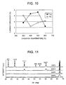
- FIG. 8 shows an X-ray diffraction pattern of the electrode 21 for electrolysis (the surface layer 25 is made of tantalum oxide) obtained as described above
- FIG. 9 shows an X-ray diffraction pattern of the electrode 21 for electrolysis (the surface layer 25 is made of tungsten oxide) obtained as described above.
- X-ray diffraction is used in the same manner as in the above example, whereby a crystal structure of tantalum oxide (tungsten oxide) constituting the surface layer 25 can be analyzed. Even in such an example, the structure was observed using an X-ray diffraction apparatus (D8 Discover manufactured by Bruker AXS Co.).
- FIG. 8 shows the X-ray diffraction patterns of the electrode 21 oxidized at 600°C, 500°C, 400°C and 300°C in order from the upside. It is to be noted that for comparison, an X-ray diffraction pattern of an electrode (having the surface only of Pt) which is not provided with the surface layer 25 is shown in the bottom.
- a diffraction peak (a peak shown by a solid circle in FIG. 8 ) inherent in tantalum oxide (Ta 2 O 5 ) and a diffraction peak (a peak shown by * in FIG. 8 ) inherent in platinum constituting the intermediate layer 24 are recognized. Therefore, it is seen that the surface layer 25 of crystalline tantalum oxide (Ta 2 O 5 ) is formed on the conditions.
- a diffraction peak (a peak shown by a black triangle in FIG. 8 ) inherent in tantalum (Ta) and a diffraction peak inherent in platinum are recognized. Therefore, it is seen that a part of the surface layer 25 remains as tantalum on the conditions.
- any diffraction peak inherent in tantalum oxide or tantalum described above is not recognized, and the diffraction peak inherent in platinum and a halo indicating an amorphous state (a non-crystalline state) are recognized. Therefore, it is seen that the surface layer 25 of amorphous tantalum oxide is formed on the conditions. It is to be noted that even in comparison with the X-ray diffraction pattern of the platinum electrode shown for comparison, it is easily seen that the amorphous state is present in the electrode on the conditions.
- FIG. 9 shows the X-ray diffraction patterns of the electrode 21 oxidized at 600°C, 500°C, 400°C and 300°C in order from the upside. It is to be noted that for comparison, an X-ray diffraction pattern of an electrode (having the surface only of Pt) which is not provided with the surface layer 25 is shown in the bottom in the same manner as described above. According to the patterns, in the electrode 21 oxidized at a temperature of 600°C, 500°C or 400°C, a diffraction peak (a peak shown by a open circle in FIG. 9 ) inherent in tungsten oxide (WO 3 ) and a diffraction peak (a peak shown by * in FIG. 9 ) inherent in platinum constituting the intermediate layer 24 are recognized. Therefore, it is seen that the surface layer 25 of crystalline tungsten oxide (WO 3 ) is formed on the conditions.
- FIG. 10 is a diagram showing an ozone forming current efficiency in a case where the electrode for electrolysis prepared on the conditions is used.
- a solid circle shows an ozone forming current efficiency in a case where the surface layer 25 is made of tantalum oxide
- a open circle shows an ozone forming current efficiency in a case where the surface layer 25 is made of tungsten oxide.
- the ozone forming current efficiency was about 3.6%.
- the ozone forming current efficiencies were about 6.6% at an oxidizing temperature of 400°C, about 7.2% at an oxidizing temperature of 500°C, and about 2.4% at an oxidizing temperature of 600°C.
- the surface layer has a crystal structure of tantalum oxide or tantalum.
- amorphous tantalum oxide which does not have any crystal structure is formed as the surface layer 25.
- the ozone forming current efficiency was about 6.1%.
- the ozone forming current efficiencies were about 2.4% at an oxidizing temperature of 400°C, about 3.6% at an oxidizing temperature of 500°C, and about 4.2% at an oxidizing temperature of 600°C.
- the surface layer has a crystal structure of tungsten oxide.
- amorphous tungsten oxide which does not have any crystal structure is formed as the surface layer 25.
- Example 3 of the present invention an electrode for electrolysis according to Example 3 of the present invention will be described. It is to be noted that a manufacturing method of an electrode 31 for electrolysis obtained according to such an example is similar to that shown in the flow chart of FIG. 2 in Example 1, and a schematic constitution diagram is substantially similar to FIG. 1 , so that detailed description of the manufacturing method is omitted.
- a close contact layer 3 of titanium oxide is formed on the surface of Si constituting a substrate by a sputtering process as described above, and an intermediate layer 4 of platinum is formed on the surface of the close contact layer 3 by the sputtering process.
- a surface layer 5 is formed on the surface of a substrate 2 provided with the intermediate layer 4.
- the surface layer 5 is formed by a spin coat process, so that the surface of the substrate 2 provided with the intermediate layer 4 is coated with an organic tantalum compound solution as a surface layer constituting material.
- the surface layer 5 of tantalum oxide is formed using a Ta(OEt) 5 solution in the present example.
- ethyl acetate is used as a solvent of the Ta(OEt) 5 solution.
- the Ta(OEt) 5 solution is used as the surface layer constituting material, but the present invention is not limited to this example.
- the material is a tantalum-containing compound which can be calcinated to remove a substance other than tantalum therefrom, thereby forming a film of tantalum oxide.
- ethyl acetate is used as the solvent, but the present invention is not limited to this example, and another solvent such as an alcohol-substrated solvent may be used.
- the surface layer constituting material is dripped on the surface of the substrate 2 provided with the intermediate layer 4 to form a thin film by the spin coat process.
- Conditions in the spin coat process according to such an example are five seconds with 1000 rpm and 15 seconds at 3000 rpm in the same manner as in Example 1. Afterward, the film is dried in an environment at room temperature for ten minutes and then at 200°C for ten minutes.
- the substrate 2 provided with the intermediate layer 4 and the surface layer 5 is calcinated (annealed) at 400°C to 700°C in a muffle furnace in the atmospheric air for ten minutes, to obtain the electrode for electrolysis.
- the surface of the intermediate layer 4 is uniformly coated with tantalum oxide as the surface layer constituting material.
- the surface layer 5 of the electrode 1 for electrolysis obtained as described above is all tantalum oxide. That is, the surface layer constituting material is a tantalum-containing compound which is calcinated as described above to remove therefrom substances other than tantalum, that is, functional groups of organic substances and the like. On the other hand, tantalum reacts with oxygen in the atmosphere to constitute tantalum oxide.
- FIG. 11 shows an X-ray diffraction pattern of the electrode 1 for electrolysis (the surface layer 5 is made of tantalum oxide) obtained as described above.
- X-ray diffraction is used in the same manner as in the above examples, whereby a crystal structure of tantalum oxide constituting the surface layer 5 can be analyzed. Even in such an example, the structure was observed using an X-ray diffraction apparatus (D8 Discover manufactured by Bruker AXS Co.).
- FIG. 11 shows the X-ray diffraction patterns of the electrode 1 calcinated at 700°C, 600°C, 500°C and 400°C in order from the upside.
- a diffraction peak (a peak shown by a solid circle in FIG. 11 ) inherent in tantalum oxide (Ta 2 O 5 ) is recognized. Therefore, it is seen that the surface layer 5 of crystalline tantalum oxide (Ta 2 O 5 ) is formed on the conditions.
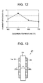
- FIG. 12 is a diagram showing an ozone forming current efficiency in a case where the electrode for electrolysis prepared on the conditions is used. It is to be noted that experiment results are obtained using an electrolysis device 10 of the above example, and a constitution of the device and experiment conditions are similar to those described above, so that description thereof is omitted.
- the ozone forming current efficiency was about 7.0%.
- the ozone forming current efficiencies were about 12.0% at a calcinating temperature of 500°C, about 6.1% at a calcinating temperature of 600°C, and about 4.6% at a calcinating temperature of 700°C.
- the surface layer has a crystal structure of tantalum oxide.
- amorphous tantalum oxide which does not have any crystal structure is formed as the surface layer 5.
- the ozone forming current efficiency is high as compared with a case where the surface layer 5 of tantalum oxide having a crystal structure is formed.
- an electrolytic solution may be electrolyzed using either electrode for electrolysis as an anode to form ozone in the electrolytic solution.
- an ozone forming efficiency is high as compared with a case where the surface layer of crystalline tantalum oxide or tungsten oxide is formed.
- an empty level right above Fermi level receives the electrons from an electrolyte, whereby an electrode reaction in the anode preferentially causes an oxygen forming reaction.
- the surface layer is made of the crystallized metal oxide, a metal segregates in a grain boundary between crystals, and a current flows. Even in this case, the empty level right above the Fermi level receives the electrons from the electrolyte, whereby the oxygen forming reaction is preferentially caused by the electrode reaction in the anode.
- the surface layer is made of an amorphous metal oxide such as amorphous tantalum oxide or tungsten oxide, so that an empty level around a bottom of a conduction band having an energy level higher as much as an about half of a band gap than the Fermi level receives the electrons from the electrolyte. Owing to the electrons, the oxygen forming reaction is suppressed unlike the above case, and instead an ozone forming reaction is more efficiently caused.
- the electrode for electrolysis according to the above examples it is supposed that the electrons move at a higher energy level to cause the ozone forming reaction, and an ozone forming efficiency rises as compared with a case where the electrode for electrolysis of platinum or the like, or the electrode for electrolysis provided with the surface layer of crystallized tantalum oxide (the crystallized metal oxide) is used.
- a current having a predetermined low current density of 0.1 mA/cm 2 to 2000 mA/cm 2 , preferably 1 mA/cm 2 to 1000 mA/cm 2 is applied to the electrode 1 for electrolysis, whereby ozone can efficiently be formed.
- the temperature of the electrolytic solution is not especially set to a low temperature and is set to ordinary temperature of +15°C as in the present example, ozone can efficiently be formed. Therefore, power consumption required for the ozone formation can be reduced.
- the surface layer 5 of the electrode 1 capable of realizing the efficient ozone formation can be formed by not only the sputtering process but also the spin coat process as described above, so that productivity can be improved.
- the electrode for electrolysis can be manufactured with low manufacturing cost, and an inexpensive equipment can be realized.
- the substrate 2 of Si is provided with the intermediate layer 4 including at least a metal which is not easily oxidized, a metal oxide having conductivity or a metal having conductivity even when oxidized, and the surface layer 5 is further formed on the surface of the intermediate layer 4 as described above, so that the electrons can effectively move in the surface layer 5. Therefore, the electrode reaction can be caused with a high energy level in the surface of the surface layer 5, and ozone can efficiently be formed with a lower current density.
- the substrate 2 is made of a material similar to that of the intermediate layer 4, that is, a material including at least a metal which is not easily oxidized, a metal oxide having conductivity or a metal having conductivity even when oxidized, it is possible to constitute an electrode capable of similarly efficiently forming ozone without being especially provided with the intermediate layer 4.
- the substrate 2 is coated with the intermediate layer 4 made of the above material as in the present invention, whereby it is possible to realize with low production cost the electrode 1 capable of similarly efficiently forming ozone.
- the electrode for electrolysis according to the examples of the present invention is not limited to the electrode shown in the electrolysis device 10, and may be used as, for example, an anode for an electrolysis unit 26 shown in FIG. 13 .
- the electrolysis unit 26 shown in FIG. 13 is constituted of the electrode 1 or 21 for electrolysis constituting the anode according to the above examples, an electrode 28 constituting the cathode, and a cation exchange film 29.
- the electrode 1 (or 21 as the anode) and the electrode 28 (the cathode) are provided with a plurality of water permeable holes 27A and 28A for securing water permeability, respectively. Then, the electrodes 1 and 28 are arranged on both surfaces of the cation exchange film (Nafion (trade name) manufactured by Dupont Co. was used in the present example) 29, to constitute the electrolysis unit 26,
- the electrolysis unit 26 is immersed in a treatment tank in which an electrolytic solution is received, and a constant current with a predetermined current density is applied between both the electrodes 1, 28.
- a constant current with a predetermined current density is applied between both the electrodes 1, 28.
- an appropriate zero gap is maintained between the electrode 1 and the cation exchange film 29 and electrode 28, and protons move in the cation exchange film 29, whereby ozone can efficiently be formed even when the electrolytic solution is pure water.
- the water permeable holes 27A and 28A allow a formed gas to flow therethrough, whereby stable ozone formation can be realized.
Landscapes
- Chemical & Material Sciences (AREA)
- Engineering & Computer Science (AREA)
- Chemical Kinetics & Catalysis (AREA)
- Electrochemistry (AREA)
- Materials Engineering (AREA)
- Metallurgy (AREA)
- Organic Chemistry (AREA)
- Inorganic Chemistry (AREA)
- Electrodes For Compound Or Non-Metal Manufacture (AREA)
- Electrolytic Production Of Non-Metals, Compounds, Apparatuses Therefor (AREA)
Applications Claiming Priority (2)
| Application Number | Priority Date | Filing Date | Title |
|---|---|---|---|
| JP2007057294 | 2007-03-07 | ||
| JP2008022524A JP2008248378A (ja) | 2007-03-07 | 2008-02-01 | 電解用電極及び電解ユニット |
Publications (2)
| Publication Number | Publication Date |
|---|---|
| EP1970471A2 true EP1970471A2 (de) | 2008-09-17 |
| EP1970471A3 EP1970471A3 (de) | 2009-05-13 |
Family
ID=39494629
Family Applications (1)
| Application Number | Title | Priority Date | Filing Date |
|---|---|---|---|
| EP08003969A Withdrawn EP1970471A3 (de) | 2007-03-07 | 2008-03-04 | Elektrode zur Elektrolyse und Elektrolyseeinheit |
Country Status (2)
| Country | Link |
|---|---|
| US (1) | US20080217168A1 (de) |
| EP (1) | EP1970471A3 (de) |
Citations (4)
| Publication number | Priority date | Publication date | Assignee | Title |
|---|---|---|---|---|
| JPH1177060A (ja) | 1997-09-04 | 1999-03-23 | Nippon Nature Roman:Kk | オゾン水生成装置 |
| JPH11333475A (ja) | 1998-05-22 | 1999-12-07 | Tokico Ltd | オゾン水生成装置 |
| JP2002080986A (ja) | 2000-09-07 | 2002-03-22 | Matsushita Electric Ind Co Ltd | オゾン発生用電極、これを用いたオゾン水製造方法及びオゾン水製造装置 |
| JP2007016303A (ja) | 2005-06-07 | 2007-01-25 | Sanyo Electric Co Ltd | 電解用電極及びその電極を用いた過硫酸溶解水の生成方法 |
Family Cites Families (5)
| Publication number | Priority date | Publication date | Assignee | Title |
|---|---|---|---|---|
| DE3616607A1 (de) * | 1985-05-17 | 1986-11-20 | Ricoh Co., Ltd., Tokio/Tokyo | Lichtempfindliches material fuer die elektrophotographie |
| KR101153978B1 (ko) * | 2002-03-26 | 2012-06-14 | 카부시키카이샤 시.브이.리서어치 | 비결정질 금속 산화막의 제조 방법 및 비결정질 금속산화막을 가지는 커패시턴스 소자와 반도체 장치를제조하는 방법 |
| KR100701555B1 (ko) * | 2002-05-22 | 2007-03-30 | 마사시 카와사키 | 반도체 장치 및 그것을 이용하는 표시 장치 |
| JP2006097122A (ja) * | 2004-08-31 | 2006-04-13 | Sanyo Electric Co Ltd | 電解用電極及び電解用電極の製造方法 |
| JP2007046129A (ja) * | 2005-08-11 | 2007-02-22 | Sanyo Electric Co Ltd | 電解用電極及び電解用電極の製造方法 |
-
2008
- 2008-03-04 EP EP08003969A patent/EP1970471A3/de not_active Withdrawn
- 2008-03-07 US US12/073,611 patent/US20080217168A1/en not_active Abandoned
Patent Citations (4)
| Publication number | Priority date | Publication date | Assignee | Title |
|---|---|---|---|---|
| JPH1177060A (ja) | 1997-09-04 | 1999-03-23 | Nippon Nature Roman:Kk | オゾン水生成装置 |
| JPH11333475A (ja) | 1998-05-22 | 1999-12-07 | Tokico Ltd | オゾン水生成装置 |
| JP2002080986A (ja) | 2000-09-07 | 2002-03-22 | Matsushita Electric Ind Co Ltd | オゾン発生用電極、これを用いたオゾン水製造方法及びオゾン水製造装置 |
| JP2007016303A (ja) | 2005-06-07 | 2007-01-25 | Sanyo Electric Co Ltd | 電解用電極及びその電極を用いた過硫酸溶解水の生成方法 |
Also Published As
| Publication number | Publication date |
|---|---|
| EP1970471A3 (de) | 2009-05-13 |
| US20080217168A1 (en) | 2008-09-11 |
Similar Documents
| Publication | Publication Date | Title |
|---|---|---|
| US20080060947A1 (en) | Electrode for electrolysis, electrolytic process using the electrode, and electrolytic apparatus using them | |
| Yang et al. | Highly acid-durable carbon coated Co3O4 nanoarrays as efficient oxygen evolution electrocatalysts | |
| US20120279853A1 (en) | Cathode, electrolytic cell for electrolysis of alkali metal chloride, and method for producing negative electrode | |
| US11898255B2 (en) | Method of producing hydrogen peroxide using nanostructured bismuth oxide | |
| JP2007046129A (ja) | 電解用電極及び電解用電極の製造方法 | |
| WO2017182923A1 (en) | Oxygen evolution electrocatalysts with carbon coated cobalt (ii, iii) oxide layers | |
| JP2015200016A (ja) | 水分解用光電極、水分解装置 | |
| KR20140013326A (ko) | 수도수 전기분해용 금속 산화물 전극 및 그 제조 방법 | |
| JP7330490B2 (ja) | オゾン生成用電極 | |
| WO2011013261A1 (ja) | 電解用電極材料、電解用電極及びその製造方法 | |
| CN101187039A (zh) | 电解用电极及使用了它的电解方法以及使用了它的电解装置 | |
| US20080217168A1 (en) | Electrode for electrolysis and electrolysis unit | |
| JP2010007144A (ja) | 電解用電極および電解ユニット | |
| KR102301857B1 (ko) | 하이포아염소산 생산을 위한 전극 및 그 제조방법 | |
| JP4290169B2 (ja) | 電解用電極及びその電極を用いた過硫酸溶解水の生成方法 | |
| CN106283104A (zh) | 非晶二氧化钛/纳米氧化铱/多孔硅阳极及其制备方法 | |
| KR20120085787A (ko) | 제어된 결정 조직을 구비한 전기 분해 공정용 전극 | |
| JP2008248378A (ja) | 電解用電極及び電解ユニット | |
| CN111847596A (zh) | 一种电解电极及其制备方法、电解装置、衣物处理设备 | |
| JP2010001552A (ja) | 電解用電極および電解ユニット | |
| JP2011174164A (ja) | 電解用電極、及びその電極の製造方法 | |
| JP2007224351A (ja) | 電解用電極及びその製造方法及びそれを用いた電解方法 | |
| RU2791363C2 (ru) | Анод для электролитического выделения хлора | |
| CN119162613A (zh) | 用于电解制氯的催化阳极和方法 | |
| Dong | Atomic Layer Deposition of Amorphous Thin Films in Surface Modification and Protection for Electrochemical and Electronic Applications |
Legal Events
| Date | Code | Title | Description |
|---|---|---|---|
| PUAI | Public reference made under article 153(3) epc to a published international application that has entered the european phase |
Free format text: ORIGINAL CODE: 0009012 |
|
| AK | Designated contracting states |
Kind code of ref document: A2 Designated state(s): AT BE BG CH CY CZ DE DK EE ES FI FR GB GR HR HU IE IS IT LI LT LU LV MC MT NL NO PL PT RO SE SI SK TR |
|
| AX | Request for extension of the european patent |
Extension state: AL BA MK RS |
|
| PUAL | Search report despatched |
Free format text: ORIGINAL CODE: 0009013 |
|
| AK | Designated contracting states |
Kind code of ref document: A3 Designated state(s): AT BE BG CH CY CZ DE DK EE ES FI FR GB GR HR HU IE IS IT LI LT LU LV MC MT NL NO PL PT RO SE SI SK TR |
|
| AX | Request for extension of the european patent |
Extension state: AL BA MK RS |
|
| STAA | Information on the status of an ep patent application or granted ep patent |
Free format text: STATUS: THE APPLICATION HAS BEEN WITHDRAWN |
|
| 18W | Application withdrawn |
Effective date: 20090701 |