EP1969284B1 - Source lumineuse plate et dispositif d'affichage l'utilisant - Google Patents
Source lumineuse plate et dispositif d'affichage l'utilisant Download PDFInfo
- Publication number
- EP1969284B1 EP1969284B1 EP06843718A EP06843718A EP1969284B1 EP 1969284 B1 EP1969284 B1 EP 1969284B1 EP 06843718 A EP06843718 A EP 06843718A EP 06843718 A EP06843718 A EP 06843718A EP 1969284 B1 EP1969284 B1 EP 1969284B1
- Authority
- EP
- European Patent Office
- Prior art keywords
- luminescent
- color
- light
- light source
- guide member
- Prior art date
- Legal status (The legal status is an assumption and is not a legal conclusion. Google has not performed a legal analysis and makes no representation as to the accuracy of the status listed.)
- Not-in-force
Links
Images


Classifications
-
- G—PHYSICS
- G02—OPTICS
- G02F—OPTICAL DEVICES OR ARRANGEMENTS FOR THE CONTROL OF LIGHT BY MODIFICATION OF THE OPTICAL PROPERTIES OF THE MEDIA OF THE ELEMENTS INVOLVED THEREIN; NON-LINEAR OPTICS; FREQUENCY-CHANGING OF LIGHT; OPTICAL LOGIC ELEMENTS; OPTICAL ANALOGUE/DIGITAL CONVERTERS
- G02F1/00—Devices or arrangements for the control of the intensity, colour, phase, polarisation or direction of light arriving from an independent light source, e.g. switching, gating or modulating; Non-linear optics
- G02F1/01—Devices or arrangements for the control of the intensity, colour, phase, polarisation or direction of light arriving from an independent light source, e.g. switching, gating or modulating; Non-linear optics for the control of the intensity, phase, polarisation or colour
- G02F1/13—Devices or arrangements for the control of the intensity, colour, phase, polarisation or direction of light arriving from an independent light source, e.g. switching, gating or modulating; Non-linear optics for the control of the intensity, phase, polarisation or colour based on liquid crystals, e.g. single liquid crystal display cells
- G02F1/133—Constructional arrangements; Operation of liquid crystal cells; Circuit arrangements
- G02F1/1333—Constructional arrangements; Manufacturing methods
- G02F1/1335—Structural association of cells with optical devices, e.g. polarisers or reflectors
- G02F1/1336—Illuminating devices
- G02F1/133602—Direct backlight
- G02F1/133609—Direct backlight including means for improving the color mixing, e.g. white
-
- G—PHYSICS
- G02—OPTICS
- G02B—OPTICAL ELEMENTS, SYSTEMS OR APPARATUS
- G02B6/00—Light guides; Structural details of arrangements comprising light guides and other optical elements, e.g. couplings
- G02B6/0001—Light guides; Structural details of arrangements comprising light guides and other optical elements, e.g. couplings specially adapted for lighting devices or systems
- G02B6/0011—Light guides; Structural details of arrangements comprising light guides and other optical elements, e.g. couplings specially adapted for lighting devices or systems the light guides being planar or of plate-like form
- G02B6/0033—Means for improving the coupling-out of light from the light guide
- G02B6/0035—Means for improving the coupling-out of light from the light guide provided on the surface of the light guide or in the bulk of it
-
- G—PHYSICS
- G02—OPTICS
- G02B—OPTICAL ELEMENTS, SYSTEMS OR APPARATUS
- G02B6/00—Light guides; Structural details of arrangements comprising light guides and other optical elements, e.g. couplings
- G02B6/0001—Light guides; Structural details of arrangements comprising light guides and other optical elements, e.g. couplings specially adapted for lighting devices or systems
- G02B6/0011—Light guides; Structural details of arrangements comprising light guides and other optical elements, e.g. couplings specially adapted for lighting devices or systems the light guides being planar or of plate-like form
- G02B6/0066—Light guides; Structural details of arrangements comprising light guides and other optical elements, e.g. couplings specially adapted for lighting devices or systems the light guides being planar or of plate-like form characterised by the light source being coupled to the light guide
- G02B6/0068—Arrangements of plural sources, e.g. multi-colour light sources
-
- G—PHYSICS
- G02—OPTICS
- G02F—OPTICAL DEVICES OR ARRANGEMENTS FOR THE CONTROL OF LIGHT BY MODIFICATION OF THE OPTICAL PROPERTIES OF THE MEDIA OF THE ELEMENTS INVOLVED THEREIN; NON-LINEAR OPTICS; FREQUENCY-CHANGING OF LIGHT; OPTICAL LOGIC ELEMENTS; OPTICAL ANALOGUE/DIGITAL CONVERTERS
- G02F1/00—Devices or arrangements for the control of the intensity, colour, phase, polarisation or direction of light arriving from an independent light source, e.g. switching, gating or modulating; Non-linear optics
- G02F1/01—Devices or arrangements for the control of the intensity, colour, phase, polarisation or direction of light arriving from an independent light source, e.g. switching, gating or modulating; Non-linear optics for the control of the intensity, phase, polarisation or colour
- G02F1/13—Devices or arrangements for the control of the intensity, colour, phase, polarisation or direction of light arriving from an independent light source, e.g. switching, gating or modulating; Non-linear optics for the control of the intensity, phase, polarisation or colour based on liquid crystals, e.g. single liquid crystal display cells
- G02F1/133—Constructional arrangements; Operation of liquid crystal cells; Circuit arrangements
- G02F1/1333—Constructional arrangements; Manufacturing methods
- G02F1/1335—Structural association of cells with optical devices, e.g. polarisers or reflectors
- G02F1/1336—Illuminating devices
- G02F1/133602—Direct backlight
- G02F1/133603—Direct backlight with LEDs
-
- G—PHYSICS
- G02—OPTICS
- G02F—OPTICAL DEVICES OR ARRANGEMENTS FOR THE CONTROL OF LIGHT BY MODIFICATION OF THE OPTICAL PROPERTIES OF THE MEDIA OF THE ELEMENTS INVOLVED THEREIN; NON-LINEAR OPTICS; FREQUENCY-CHANGING OF LIGHT; OPTICAL LOGIC ELEMENTS; OPTICAL ANALOGUE/DIGITAL CONVERTERS
- G02F1/00—Devices or arrangements for the control of the intensity, colour, phase, polarisation or direction of light arriving from an independent light source, e.g. switching, gating or modulating; Non-linear optics
- G02F1/01—Devices or arrangements for the control of the intensity, colour, phase, polarisation or direction of light arriving from an independent light source, e.g. switching, gating or modulating; Non-linear optics for the control of the intensity, phase, polarisation or colour
- G02F1/13—Devices or arrangements for the control of the intensity, colour, phase, polarisation or direction of light arriving from an independent light source, e.g. switching, gating or modulating; Non-linear optics for the control of the intensity, phase, polarisation or colour based on liquid crystals, e.g. single liquid crystal display cells
- G02F1/133—Constructional arrangements; Operation of liquid crystal cells; Circuit arrangements
- G02F1/1333—Constructional arrangements; Manufacturing methods
- G02F1/1335—Structural association of cells with optical devices, e.g. polarisers or reflectors
- G02F1/1336—Illuminating devices
- G02F1/133602—Direct backlight
- G02F1/133606—Direct backlight including a specially adapted diffusing, scattering or light controlling members
-
- H—ELECTRICITY
- H01—ELECTRIC ELEMENTS
- H01L—SEMICONDUCTOR DEVICES NOT COVERED BY CLASS H10
- H01L25/00—Assemblies consisting of a plurality of individual semiconductor or other solid state devices ; Multistep manufacturing processes thereof
- H01L25/03—Assemblies consisting of a plurality of individual semiconductor or other solid state devices ; Multistep manufacturing processes thereof all the devices being of a type provided for in the same subgroup of groups H01L27/00 - H01L33/00, or in a single subclass of H10K, H10N, e.g. assemblies of rectifier diodes
- H01L25/04—Assemblies consisting of a plurality of individual semiconductor or other solid state devices ; Multistep manufacturing processes thereof all the devices being of a type provided for in the same subgroup of groups H01L27/00 - H01L33/00, or in a single subclass of H10K, H10N, e.g. assemblies of rectifier diodes the devices not having separate containers
- H01L25/075—Assemblies consisting of a plurality of individual semiconductor or other solid state devices ; Multistep manufacturing processes thereof all the devices being of a type provided for in the same subgroup of groups H01L27/00 - H01L33/00, or in a single subclass of H10K, H10N, e.g. assemblies of rectifier diodes the devices not having separate containers the devices being of a type provided for in group H01L33/00
- H01L25/0753—Assemblies consisting of a plurality of individual semiconductor or other solid state devices ; Multistep manufacturing processes thereof all the devices being of a type provided for in the same subgroup of groups H01L27/00 - H01L33/00, or in a single subclass of H10K, H10N, e.g. assemblies of rectifier diodes the devices not having separate containers the devices being of a type provided for in group H01L33/00 the devices being arranged next to each other
-
- G—PHYSICS
- G02—OPTICS
- G02F—OPTICAL DEVICES OR ARRANGEMENTS FOR THE CONTROL OF LIGHT BY MODIFICATION OF THE OPTICAL PROPERTIES OF THE MEDIA OF THE ELEMENTS INVOLVED THEREIN; NON-LINEAR OPTICS; FREQUENCY-CHANGING OF LIGHT; OPTICAL LOGIC ELEMENTS; OPTICAL ANALOGUE/DIGITAL CONVERTERS
- G02F1/00—Devices or arrangements for the control of the intensity, colour, phase, polarisation or direction of light arriving from an independent light source, e.g. switching, gating or modulating; Non-linear optics
- G02F1/01—Devices or arrangements for the control of the intensity, colour, phase, polarisation or direction of light arriving from an independent light source, e.g. switching, gating or modulating; Non-linear optics for the control of the intensity, phase, polarisation or colour
- G02F1/13—Devices or arrangements for the control of the intensity, colour, phase, polarisation or direction of light arriving from an independent light source, e.g. switching, gating or modulating; Non-linear optics for the control of the intensity, phase, polarisation or colour based on liquid crystals, e.g. single liquid crystal display cells
- G02F1/133—Constructional arrangements; Operation of liquid crystal cells; Circuit arrangements
- G02F1/1333—Constructional arrangements; Manufacturing methods
- G02F1/1335—Structural association of cells with optical devices, e.g. polarisers or reflectors
- G02F1/1336—Illuminating devices
- G02F1/133614—Illuminating devices using photoluminescence, e.g. phosphors illuminated by UV or blue light
-
- H—ELECTRICITY
- H01—ELECTRIC ELEMENTS
- H01L—SEMICONDUCTOR DEVICES NOT COVERED BY CLASS H10
- H01L2924/00—Indexing scheme for arrangements or methods for connecting or disconnecting semiconductor or solid-state bodies as covered by H01L24/00
- H01L2924/0001—Technical content checked by a classifier
- H01L2924/0002—Not covered by any one of groups H01L24/00, H01L24/00 and H01L2224/00
-
- H—ELECTRICITY
- H01—ELECTRIC ELEMENTS
- H01L—SEMICONDUCTOR DEVICES NOT COVERED BY CLASS H10
- H01L33/00—Semiconductor devices with at least one potential-jump barrier or surface barrier specially adapted for light emission; Processes or apparatus specially adapted for the manufacture or treatment thereof or of parts thereof; Details thereof
- H01L33/48—Semiconductor devices with at least one potential-jump barrier or surface barrier specially adapted for light emission; Processes or apparatus specially adapted for the manufacture or treatment thereof or of parts thereof; Details thereof characterised by the semiconductor body packages
- H01L33/50—Wavelength conversion elements
- H01L33/501—Wavelength conversion elements characterised by the materials, e.g. binder
- H01L33/502—Wavelength conversion materials
- H01L33/504—Elements with two or more wavelength conversion materials
Definitions
- the present invention relates to a light guide member for a flat light source device, a flat light source device using the light guide member, and a display device provided with the flat light source device that are used as a back light for a liquid crystal display for instance.
- the main stream of such a back light for a liquid crystal display has been the so-called edge light type in which a cold cathode tube as a light source is disposed on the edge face of the chassis for thinning and low power consumption of the apparatus (Japanese Patent Publication No. 2732492 ).
- edge light type in which a cold cathode tube as a light source is disposed on the edge face of the chassis for thinning and low power consumption of the apparatus.
- Japanese Patent Publication No. 2732492 Japanese Patent Publication No. 2732492
- the edge light type has a limitation in improving a luminance and a uniformity in the luminance. Therefore, an adoption of a direct lighting type light has been examined for a large size liquid crystal display.
- Fig. 5 is a cross sectional view for showing a configuration of a conventional planar light source device of a direct lighting type used in a liquid crystal display (TECHNO-FRONTIER SYMPOSIUM 2005, Thermal Design and Countermeasure Technology Symposium, Issue Date: April 20, 2005 (Japan Management Association), Session G3: Latest Design Case of Heat Radiation Mounting I (pp. G3-3-1 to G3-3-4 ) and so on).
- the flat light source device 11 is disposed directly below a liquid crystal panel 21.
- LED light sources 1 using a light emitting diode device are disposed in an array pattern on a bottom face of a chassis 12, and the LED light sources 1 have a plurality of luminescent colors different from each other such as three colors of RGB. Moreover, the bottom face and side faces of the chassis 12 are covered with a reflecting sheet 13. Furthermore, over the LED light sources 1, a diffusing sheet 14 and a prism sheet 15 are disposed in the range of 1 to 5 cm in general apart from the LED light sources 1.
- the emitted light travels directly toward the diffusing sheet 14, or is reflected by the reflecting sheet 13 and travels toward the diffusing sheet 14.
- the emitted light is then irregularly reflected in the diffusing sheet 14, and is inclined in a vertical direction by passing through the prism sheet 15.
- the emitted light then enters a liquid crystal panel 21.
- Lights emitted from different LED light sources 1 are mixed in a space between the LED light sources and the diffusing sheet 14. The mixing is then improved by an irregular reflection in the diffusing sheet 14, thereby implementing a uniform luminance and a uniform chromaticity.
- the diffusing sheet is made further apart from the LED light sources, unevenness of colors can be reduced to a certain level by a spatial color mixture.
- this method causes a thickness of a back light to be enlarged, and is not preferable for a flat panel display.
- the flat light source device of a direct lighting type in order to further improve a uniform chromaticity and suppress a thickness of the flat light source device, it is effective to dispose a light guide plate that faces to LED light sources in front of a substrate in which a plurality of LED light sources is disposed and to dispose a reflecting layer on the back face of the light guide plate, thereby propagating and diffusing a light that has been emitted from each LED light source in a horizontal direction in the light guide plate and then extracting the light forward.
- the disposed position of the LED light sources has a certain restriction in consideration of a heat radiation from an LED chip and a circuit design of a substrate on which an LED chip is disposed. Consequently, the relative positions of luminous origins of luminance colors different from each other such as RGB are restricted, thereby causing a sufficient color mixture to be restricted.
- a resin layer in which the inorganic fluorescent material particles such as YAG-Ce have been dispersed is formed on the periphery of an LED bare chip that has been face-down bonded to a substrate, and, for instance, a blue light emitted from a blue LED bare chip is mixed to a yellow fluorescence emitted from the inorganic fluorescent material particles that has been excited by a light emitted from the blue LED bare chip, thereby emitting a white color light as a whole.
- a light emitted from the above white LED light source is visually white, a luminance characteristic in a visible light wave length area is not flat and a wavelength distribution of a luminance has a deflection.
- a color filter of RGB is disposed on a liquid crystal panel, and each color of RGB is extracted for every picture element through a color filter which a white light emitted from a white back light passes.
- a blue LED light and a yellow fluorescence is mixed to obtain a white color
- a strength of a red color area that is on the longest wave side of a visible light wave length area is weaker than a strength of other wave length areas. Consequently, a color of a light that has passed through a red filter is unnatural and a color rendering property is not satisfactory.
- an inorganic particle As a fluorescent material of a conventional white LED light source, an inorganic particle is used as described above. However, in the case in which a resin plate in which such inorganic particles are dispersed is used for a light guide plate to which a sufficient light propagation property is required, the inorganic particle becomes a dispersion origin and prevents a light propagation in a horizontal direction, and the function of a light guide plate for diffusing lights emitted from each LED light source is lost.
- the above light source in which an LED bare chip is combined with a fluorescent material of a single kind is not indicated to be applied to a light guide plate having functions for introducing lights emitted from each LED light source disposed on the back side into one plate having a light propagation property, for propagating and diffusing the lights in a horizontal direction in the plate, and for emitting the lights forward.
- An object of the present invention is to provide a flat light source device using a light guide member, and a display device, by which a white light having a high color rendering property can be obtained without using luminescent devices of a plurality of colors.
- the present invention is defined in claim 1 and involves the following modes (1) to (8).
- the light guide member involves both types in which the luminescent device is disposed directly below the light guide member apart from the bottom face of the light guide member as shown in Fig. 2-F , and in which the luminescent device is integrated with (buried in) the inside portion at the bottom of the light guide member as shown in Figs. 2-A to 2-E .
- the expression of disposing the luminescent device "below" the light guide member can be applied to the both types. In the latter case, for the light guide member and the luminescent device integrated with each other, the section from which the luminous device is excluded is a light guide member.
- a monochromatic luminescent device of one of the purple to blue colors is used as an light source.
- the light guide member can ensure a sufficient transparency and a sufficient light propagation property even in the area containing the luminescent substance.
- the light guide member of the invention in which the organic luminescent substances are dissolved in a resin material is different from that in which inorganic particles are dispersed in a resin material.
- the area containing the luminescent substance has the both functions as a light source emitting a light other than the purple to blue color lights and as a light guide portion for propagating lights in a horizontal direction and for diffusing the lights.
- the present invention uses only a monochromatic luminescent device as a light source, lights emitted from luminescent substances contained in the second and third areas of the light guide plate become dummy light sources of other colors on the longer wave side.
- the second and third areas with luminescent colors different from each other and the first area that does not contain a luminescent substance except for the second and third areas are integrated with the light guide member. Consequently, a light of the first color of the purple to blue colors, which is guided from the luminescent device to the light guide member, and lights of the second and third colors emitted from the second and third areas in the light guide member, for instance, lights of other colors such as green and red, are propagated in a horizontal direction in the light guide member by a reflection at the upper and bottom faces of the light guide member. The lights are then diffused, mixed to each other, and extracted forward as white lights.
- the white lights extracted from a flat light source device include the purple to blue color lights emitted from luminescent devices and lights of other colors emitted from the second and third areas, such as green and red colors, thereby obtaining a flat luminance characteristic close to that of a natural light in a visible light wavelength area and obtaining a white light having a high color rendering property.
- the second and third areas in which a luminescent substance has been dissolved are excited and emit lights by a light that has been emitted from the luminescent device, that has entered the light guide member, and that has been propagated in a horizontal direction, even in the case in which the second and third areas are not disposed directly over the luminescent device. Therefore, the second and third areas as a dummy light source can be formed in a desired shape at a desired position in the light guide member. Consequently, as compared with the case in which luminescent devices with a plurality of colors are used, restrictions to the position of a light source are greatly reduced and it becomes easy to obtain a color mixture. As a result, unevenness of colors of white color lights emitted from the flat light source device can be reduced.
- the second and third areas can be freely formed in a continuous or discrete manner in the light guide member regardless of the position and number of luminescent devices such as a blue LED light source. Consequently, the present invention is of great advantage to make a color of a light white and to thin a back light.
- a white light having a high color rendering property can be obtained without using LED light sources of a plurality of colors.
- the display apparatus related to the present invention a high quality image can be obtained since the display apparatus such as a liquid crystal display is configured with the above flat light source device as a back light.
- FIG. 1 is a view showing an entire configuration of an example of a liquid crystal display device to which an embodiment of the present invention is applied.
- a liquid crystal display device in which the embodiment is applied includes, as a flat light source device of a direct lighting type (back light) 50, a back light flame (chassis) 51 that accommodates a light emitting part and an LED substrate (mounting substrate) 52 as a substrate in which a plurality of light emitting diodes (LED) 53, which is a solid-state lighting device, are arranged as light sources.
- back light direct lighting type
- lamp back light flame
- LED substrate mounting substrate
- LED light emitting diodes
- the back light device 50 includes a light guide member 54 which is a feature of the present invention, and which is accommodated in the back light flame (chassis) 51.
- the difference from a conventional direct lighting type back light device as shown in Fig. 12 lies in that the light guide member interposes in a space between the light emitting diodes and the diffusing sheet, thereby enabling to shorten an interval between the light emitting diodes and the diffusing sheet without increasing a thickness of the back light.
- the light guide member As a laminate of optical compensation sheets, it is equipped with a diffusing sheet 55 that diffuses and scatters a light to render a uniform brightness to the entire surface, and prism sheets 56, 57 that are grating films which exhibit a light collection effect to the forward direction.
- a liquid crystal display module 60 it is equipped with a liquid crystal panel 61 in which a liquid crystal is sandwiched between two glass substrates, and polarizing plates (polarizing filters) 62, 63 for restricting a vibration of a light wave to a certain direction.
- polarizing plates polarizing filters
- liquid display device is arranged with peripheral members, e.g., a driver LSI (not shown).
- peripheral members e.g., a driver LSI (not shown).
- the liquid crystal panel 61 is constituted with including many kinds of components that are not shown in the figure. For instance, it is equipped with a display electrode, an active device such as a TFT (Thin Film Transistor), and a liquid crystal, a spacer, a sealing agent, an alignment film, a common electrode, a protection film, a color filter, etc., which are not shown, on or between the two glass substrates.
- a display electrode an active device such as a TFT (Thin Film Transistor)
- TFT Thin Film Transistor
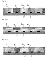
- Figs. 2-A to 2-F are partially cross sectional views showing embodiments and examples of a flat light source device related to the present invention
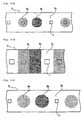
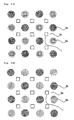
- Figs. 3-A to 3-E are partial top views showing embodiments and examples of a flat light source device related to the present invention.
- the flat light source device related to the present embodiment is used as a white back light of a liquid crystal display.
- a plurality of LED light sources 1 for emitting a blue light is disposed on upper face side of a substrate 3.
- a base material is a resin capable of propagating a light on a plurality of the LED light sources 1.
- a plurality of green color luminescent areas 2a containing an organic luminescent substance of which a radiation peak wavelength is in the range of 490 to 560 nm (the above second areas)
- the LED light sources 1 are disposed below the resin independent areas 2c that do not contain an organic luminescent substance of the light guide member 2 (the above first areas), below the green color luminescent areas 2a, and below the red color luminescent areas 2b.
- a part of the green lights is propagated in a horizontal direction while repeating a reflection at the upper and bottom faces of the light guide member 2.
- the LED light sources 1 are not disposed below the green color luminescent areas 2a and below the red color luminescent areas 2b, and the LED light sources 1 are disposed only below the resin independent areas 2c that do not contain an organic luminescent substance.
- lights emitted from the LED light sources 1 enter the light guide member 2, and a part of the lights is propagated in a horizontal direction while repeating a reflection at the upper and bottom faces. A part of the propagated lights then enters the green color luminescent areas 2a, and excites the organic luminescent substances contained in the green color luminescent areas 2a to generate a green color. A part of the green lights is propagated in a horizontal direction while repeating a reflection at the upper and bottom faces of the light guide member 2.
- lights emitted from the LED light sources 1 enter the light guide member 2, and a part of the lights propagated in a horizontal direction then enters the red color luminescent areas 2b, and excites the organic luminescent substances contained in the red color luminescent areas 2b to generate a red color.
- a part of the red lights is propagated in a horizontal direction while repeating a reflection at the upper and bottom faces of the light guide member 2.
- the flat light source device related to the present invention is provided with a plurality of luminescent devices of which a radiation peak wavelength is in the range of 380 to 490 nm and a light guide member disposed thereon.
- the luminescent devices such as LED light sources are arrayed on the substrate apart from each other linearly as shown in Figs. 3-A to 3-C , or in an array pattern as shown in Figs. 3-D and 3-E .
- the LED light source is provided with, for instance, a light emitting diode device with a size in the range of several hundreds ⁇ m to 1 mm.
- a bare chip type a type in which a light emitting diode device is mounted in a package
- a type in which a light emitting diode device is integrated with a member having a lens function, and so on.
- a substrate on which LED light sources are disposed there is mentioned, for instance, a substrate in which a circuit is formed for supplying a current to an LED light source or a laminate of a circuit substrate and a radiating substrate. An anode and a cathode of the LED light source are electrically connected to an electrode pad on the circuit substrate.
- a method of obtaining the circuit substrate there is mentioned, for instance, a method of bonding a copper foil to an insulating resin substrate such as a glass epoxy substrate and etching the copper foil in a circuit pattern.
- the heat radiating substrate is a substrate made of a material with a high thermal conductivity, such as a metal such as aluminum, copper, and a stainless steel, or a ceramics such as aluminum nitride.
- a method of fixing an LED light source onto the substrate there is mentioned, for instance, a method of a connection by using a connecting means with a small thermal resistance, such as a method of forming a through hole at the section in which an LED light source is mounted in the circuit substrate and of bonding the LED light source onto the radiating substrate exposed to the through hole by using a silver paste or a thermal conductivity silicone, and a method of thermally melting a metal such as a lead solder and a gold-tin eutectic solder and connecting the anode and cathode of a bare chip with the electrode pad of the circuit substrate by means of a face down bonding through a bump.
- a metal such as a lead solder and a gold-tin eutectic solder
- the light guide member is a member in a plate (sheet) shape made of a transparent material capable of propagating a light, and preferably is formed by a resin as a base material.
- a thickness of the light guide member is, for instance, in the range of 0.2 to 20 mm.
- the light guide member is provided with the first to third areas inside.
- the first area is made of the resin independently.
- the second area there is dissolved in the resin a luminescent substance that generates a second color having a radiation peak wavelength at a wavelength different from a radiation peak wavelength of a luminescent device of the first color by an excitation due to a light emitted from the luminescent device of the first color.
- the resin In the third area, there is dissolved in the resin a luminescent substance that generates a third color having a luminous wave length peak at a wave length different from the radiation peak wavelengths of luminescent devices of the first and second colors by an excitation due to a light emitted from the luminescent device of the first color.
- the second area is a green color luminescent area and the third area is a red color luminescent area.
- the green color luminescent area contains an organic luminescent substance that mainly emits a light of a green wavelength area by a light emitted from a luminescent device
- the red color luminescent area contains an organic luminescent substance that mainly emits a light of a red wavelength area by a light emitted from a luminescent device.
- the organic luminescent substance contained in the green color luminescent area preferably has a wide absorption edge extending to a blue wavelength area on the long wave side and a luminescent peak at a wavelength in the range of 490 to 560 nm, and is excited by a light emitted from a luminescent device to emit a fluorescence or a phosphorescence.
- the organic luminescent substance contained in the red color luminescent area preferably has a wide absorption edge extending to a blue wavelength area on the long wave side and a luminescent peak at a wave length of 605 nm or longer, and is excited by a light emitted from a luminescent device to emit a fluorescence or a phosphorescence.
- a light guide member there is improved a mixture of a light of which the main component is a blue color emitted from the luminescent device, a light of which the main component is a green color emitted from the green color luminescent area, and a light of which the main component is a red color emitted from the red color luminescent area.
- the mixture of the three primary colors enables a white color to be emitted from the flat light source device.
- a white color can also be obtained by properly selecting an organic luminescent substance to be contained in the second and third areas to emit a yellow light and an orange light from the areas, and by mixing the lights with the purple to blue lights emitted from the luminescent device.
- an organic luminescent substance to be contained in the second and third areas to emit a yellow light and an orange light from the areas, and by mixing the lights with the purple to blue lights emitted from the luminescent device.
- a combination of a green color from the second area and an orange color from the third area there is mentioned a combination of a green color from the second area and an orange color from the third area.
- the organic luminescent substance is used as a base material of the light guide member.
- the organic luminescent substance can be dissolved in a resin such as an epoxy resin and an acrylic resin, and has an absorption band in a wavelength area of ultraviolet or blue and a luminescent peak on the longer wave side.
- a resin such as an epoxy resin and an acrylic resin
- a transition metal complex and a rare earth metal complex of which a ligand is an organic molecule having a nitrogen-included heterocyclic structure are mentioned.
- a ligand that is used for the metal complexes as described above there are mentioned acetylacetonato, 2,2'-bipyridine, 9,4'-dimethyl-2,2'-bipyridine, 1,10-phenanthroline, 2-phenylpyridine, porphyrin, phthalocyanine, pyrimidine, quinoline, isoquinoline, and a derivative thereof.
- ligands of one or plural kinds are coordinated for one complex.
- an intensity distribution of a fluorescence has a peak in a wave length area of a red color
- an iridium complex indicated by the following formula (II).
- the above organic luminous substance can be dissolved in a resin that is the base material of a light guide member, and even a small amount to be used enables a high wavelength conversion efficiency to be obtained.
- the organic luminescent substance has the configuration described in Japanese Laid-Open Patent Publication No. 2003-77675 , that is, a nonionic exited site is a part of a polymer or is combined with a polymer, and the luminous portion is formed by constraining metal atoms at one or more portions of the polymer.
- the organic luminescent substance that emits phosphorescence from an excitation triplet state can also be used.
- the light guide member with which the first to third areas have been integrated can be fabricated, for instance, by using a transparent resin as a base material, preparing a plate member in which a depression, a through hole, or a groove has been formed at the section in which the second and third areas are to be formed, and injecting a resin solution in which the organic luminescent substance has been dissolved into the depression or the like, and hardening the resin solution.
- the light guide plate can also be fabricated by fabricating a resin pellet in which the organic luminescent substance has been dissolved, and fitting the resin pellet into a depression formed in a separate transparent plate, or injecting a resin solution in a frame in which a plurality of resin pellets have been arranged, and hardening the resin solution.
- the second and third areas can be formed in any shape at any position of the light guide member if necessary.
- the second and third areas can be formed in such a manner that the section containing the organic luminescent substance leads from the upper face to the bottom face as shown in Figs. 2-A and 2-D , or in such a manner that the section containing the organic luminescent substance is not the entire section in a thickness direction but a part in a thickness direction as shown in Figs. 2-B and 2-E .
- the peripheral shape of the second and third areas can also be a shape other than a vertical face in a thickness direction of the light guide member, for instance, a shape having an angle in a thickness direction of the light guide member as shown in Fig. 2-C .
- a shape of the second and third areas in a plane direction of the light guide member can be any shape such as a circular shape as shown in Fig. 3-A and a rectangular shape as shown in Fig. 3-B .
- Figs. 3-A and 3-B illustrate an embodiment in which LED light sources 1 are arranged linearly in series and the LED light sources 1 are disposed below the green color luminescent areas 2a, the red color luminescent areas 2b, and the resin independent areas 2c in the light guide member 2
- Fig. 3-C illustrates an example in which LED light sources 1 are arranged linearly in series and the LED light sources 1 are disposed only below the resin independent areas 2c in the light guide member 2.
- Fig. 3-D illustrates an embodiment in which LED light sources 1 are arranged in an array-like manner and the LED light sources 1 are disposed below the green color luminescent areas 2a, the red color luminescent areas 2b, and the resin independent areas 2c in the light guide member 2
- Fig. 3-E illustrates an example in which LED light sources 1 are arranged in an array pattern and the LED light sources 1 are disposed only below the resin independent areas 2c in the light guide member 2.
- the arrangement of the first to third areas in the light guide member 2 is properly determined in consideration of the disposition of the luminescent devices such as LED light sources in such a manner that unevenness of colors become less and a flat luminance characteristic can be obtained in consideration of a color rendering property.
- the first to third areas are disposed in such a manner that a unit arrangement composed of one point of R, one point of G, and one point of B as a unit; of one point of R, two points of G, and one point of B as a unit; or of two points of R, two points of G, and one point of B as a unit, is regularly formed in the light guide member.
- a red color luminescent area for instance, in the case in which an arrangement of two points of R, two points of G, and one point of B that are linearly disposed is a unit, there are arranged a red color luminescent area, a green color luminescent area, a resin independent area, a green color luminescent area, and a red color luminescent area in this order in the light guide member.
- a depression 4a can be formed at a position directly over a luminous device such as an LED light source 1 on the back face of the light guide member 2.
- a depression 4b can also be formed at a position directly over a luminescent device such as an LED light source 1 or at a position between the positions directly over a luminescent device on the front face of the light guide member 2.
- a shape of the depressions 4a and 4b is, for instance, a circular cone, a pyramid, a circular cylinder, a prism, or a hemi-sphere.
- the depression 4a is formed at the position directly over the luminescent device, over which a luminance of the light guide member is highest, thereby suppressing an unevenness of luminance caused by a higher luminance of the light guide member at the position in front of the luminescent device. Consequently, a uniformity of a luminance distribution can be improved on the light emitting face of the light guide member.
- the depression 4b is also formed on the front face of the light guide member 2, thereby improving a uniformity of a luminance distribution on the light emitting face of the light guide member.
- a light scattering dot can be formed on the front face and the back face of the light guide member in order to improve a uniformity of a luminance if necessary.
- the light scattering dot can be formed by the dot printing of a scattering ink or the integral molding with the light guide member.
- a reflecting part can be disposed on the back face of the light guide member if necessary.
- a white reflecting sheet bonded to the back face of the light guide member, a film of a white paint printed on the back face of the light guide member, and a white reflecting layer formed on the circuit substrate.
- a diffusing sheet is preferably disposed a distance in the range of 1 to 5 cm apart preferably.
- the luminescent devices such as LED light sources are disposed on the bottom of the chassis in which the bottom face and the side face are covered with a reflecting sheet, and a diffusing sheet is disposed on the upper face side of the chassis.
- Fig. 4 shows the entire configuration of a flat light source device related to an embodiment of the present invention.
- the flat light source device 11 is configured similarly to the prior art shown in Fig. 5 except that there is used only a monochromatic LED light source that is a luminescent device of the first color and that a light guide member 2 is disposed.
- the flat light source device 11 is disposed directly below a liquid crystal panel 21.
- LED light sources 1 are disposed in an array-like manner on a bottom face of a chassis 12, and the bottom face and side faces of the chassis 12 are covered with a reflecting sheet 13.
- the light guide member 2 is disposed over the LED light sources 1, and over the light guide member 2, a diffusing sheet 14 and a prism sheet 15 are disposed in the range of 1 to 5 cm in general apart from the LED light sources 1.
- the display apparatus related to the present invention is provided with the flat light source device as described above.
- a display portion of the display device is a liquid crystal panel
- the flat light source device is disposed on the back face of the liquid crystal panel as a back light as shown in Fig. 4 .
- An iridium complex of 8 mg of the above described formula (II) was dissolved in the epoxy resin (product name: NLD-SL-1101 manufactured by SANYU REC CO. LTD.) of 10 g and degassed.
- the iridium complex was then filled in a metal mold made of an aluminum alloy capable of fabricating a cylindrical pellet with a diameter of 6 mm and a thickness or 1 mm, and heated at 100°C for two hours and then at 130°C for three hours to fabricate a pellet capable of emitting a red light.
- a pellet capable of emitting a green light was fabricated by using an iridium complex of 30 mg of the above described formula (I) and an epoxy resin of 10 g. Moreover, a pellet made of only an epoxy resin without containing an iridium complex was also fabricated.
- a white insulating layer with a thickness of 40 ⁇ m was then formed on a square aluminum base plate with a side of 50 mm and with a thickness of 1 mm.
- four blue LED bare chip illuminants of a gallium nitride type with a total radiant flux of 70 mW, a peak wave length of 455 nm, and longitudinal and transverse sides of a 1 mm size were arranged linearly at a 10 mm pitch, and four lines of the arrangement were disposed in parallel at a 10 mm pitch.
- blue LED bare chip light sources were also disposed at the middle positions between adjacent lines and at the positions 5 mm shifted upward and downward from the line connecting adjacent light sources. Consequently, there was fabricated a substrate capable of lighting 25 blue LED bare chip light sources as the entire substrate.
- An LED driving wiring pattern on the substrate can independently drive in parallel the four lines of four serial driving and the three lines of three serial driving.
- the above substrate was buried in an iron frame with inside dimensions of longitudinal 50 mm x transverse 50 mm and a height of 3 mm, in which Teflon (registered trademark) processing was carried out to the surface.
- Teflon registered trademark
- the sealing up was then carried out to the bottom of the form to prevent a sealing resin from flowing out from a bottom gap, and the epoxy resin (product name: NLD-SL-1101 manufactured by SANYU REC CO. LTD.) was filled in the form up to the whole form (a height from the upper face of the substrate is approximately 2 mm).
- a pellet capable of emitting a red light and a pellet capable of emitting a green light were fitted into the epoxy resin depressions on the line on which four blue LED chip light sources were arranged in series in such a manner that the pellets were disposed by turns.
- a pellet made of only an epoxy resin containing no iridium complex was fitted onto a line on which three blue LED chip light sources were arranged in series, and there was fabricated finally a planar light source device of a type of Fig. 2-B and corresponding to Fig. 3-D .
- An unhardened resin solution capable of emitting a red light was made by dissolving an iridium complex of 4 mg of the above described formula (II) into the epoxy resin (product name: NLD-SL-1101 manufactured by SANYU REC CO. LTD.) of 10 g and degassing. Moreover, an unhardened resin solution capable of emitting a green light was made by dissolving and degassing an iridium complex of 15 mg of the above described formula (I) into the epoxy resin of 10 g.
- the above unhardened resin solutions and an unhardened resin solution made of only an epoxy resin without containing an iridium complex were supplied up to a height of approximately 2 mm in the washer hole by using a dispenser apparatus.
- the heating at 130°C for five hours was carried out to form a red color luminescent area, a green color luminescent area, and a resin independent area in a cylindrical shape with a diameter of 5 mm and a height of 2 mm over the blue LED bare chip light sources.
- the arrangement of the above areas is equivalent to that on the substrate fabricated in Example 1.
- the above substrate was buried in an iron frame with inside dimensions of longitudinal 50 mm x transverse 50 mm and a height of 3 mm, in which Teflon (registered trademark) processing was carried out to the surface.
- Teflon registered trademark
- the sealing up was then carried out to the bottom of the frame to prevent a sealing resin from flowing out from a bottom gap, and the epoxy resin was filled in the frame up to the whole frame (a height from the upper face of the substrate is approximately 2 mm).
- the heating at 130°C for five hours was carried out to obtain a substrate in which an epoxy transparent resin was buried in areas other than the above cylindrical areas.
- Each of the substrates fabricated in Examples 1 and 2 was disposed and fixed to an aluminum chassis with a front face opened with a bottom face of longitudinal 60 mm x transverse 60 mm and with a depth of 30 mm.
- a reflecting layer in which white reflecting films (product name: Lumirror 60L (registered trademark) manufactured by Toray Industries, Inc.) were bonded to each other was formed on the inside faces of the chassis except for the opening portion.
- a diffusing sheet (polycarbonate, product name: PC9391-50HL manufactured by TEIJIN CHEMICALS LTD.) was fixed to the front face of the opening portion of the aluminum chassis to fabricate a planar light source device corresponding to Figs. 3-D and 4 .
- a current of 220 mA was applied to the series line of four LEDs over which the red color luminescent area and the green color luminescent area were formed, a current of 60 mA was applied to the series line of three LEDs over which the resin independent area made of only an epoxy resin was formed, and a total average luminance and a chromaticity coordinate on the diffusing sheet were measured by the colorimeter (product name: CS1000 manufactured by Konica Minolta, Inc.).
- Example 3 For the flat light source device of Example 3 fabricated using the substrates fabricated in Examples 1 and 2, no current was applied to the series line of four LEDs over which the red color luminescent area and the green color luminescent area were formed, a current of 250 mA was applied to the series line of three LEDs over which the resin independent area made of only an epoxy resin was formed, and a total average luminance and a chromaticity coordinate on the diffusing sheet were measured by the colorimeter (product name: CS1000 manufactured by Konica Minolta, Inc.).
- the red color luminescent area and the green color luminescent area were not excited for a light emission by the blue LED bare chip light sources thereunder, but were excited for a light emission by a light propagated in the epoxy resin from a near blue LED bare chip light source. Consequently, this configuration corresponds to that of Fig. 3-E .
- the measured results are listed in Table 1.
- Example 3 Average luminance (cd/m 2 ) Luminance dispersion (%) Average chromaticity (X, Y) Chromaticity dispersion ( ⁇ X, ⁇ Y)
- Example 3 (substrate of Example 1) 16000 9 (0.29, 0.29) (0.008, 0.009)
- Example 3 (substrate of Example 2) 21000 13 (0.29, 0.29) (0.013, 0.018)
- Example 4 (substrate of Example 1) 4800 22 (0.22, 0.25) (0.031, 0.025)
- Example 4 substrate of Example 2) 3700 27 (0.21, 0.24) (0.039, 0.030)
Landscapes
- Physics & Mathematics (AREA)
- General Physics & Mathematics (AREA)
- Nonlinear Science (AREA)
- Optics & Photonics (AREA)
- Engineering & Computer Science (AREA)
- Crystallography & Structural Chemistry (AREA)
- Chemical & Material Sciences (AREA)
- Mathematical Physics (AREA)
- Power Engineering (AREA)
- Microelectronics & Electronic Packaging (AREA)
- Condensed Matter Physics & Semiconductors (AREA)
- Computer Hardware Design (AREA)
- Planar Illumination Modules (AREA)
- Liquid Crystal (AREA)
Abstract
Claims (6)
- Dispositif de source lumineuse plate comprenant :des dispositifs luminescents d'une première couleur ayant une longueur d'onde du maximum de rayonnement comprise dans la plage de 380 à 490 nm, etun élément de guidage de la lumière qui est constitué d'une résine transparente et qui est disposé sur un substrat sur lequel sont montés les dispositifs luminescents d'une première couleur, pour la diffusion de la lumière émise par les dispositifs luminescents et le guidage de la lumière vers le haut, l'élément de guidage de la lumière comprenant :une première région constituée de la résine seule ;une deuxième région dans laquelle est dissoute dans la résine une substance luminescente qui génère une deuxième couleur ayant une longueur d'onde du maximum de rayonnement à une longueur d'onde différente de la longueur d'onde du maximum de rayonnement d'un dispositif luminescent de la première couleur sous l'effet d'une excitation due à une lumière émise par le dispositif luminescent de la première couleur, etune troisième région dans laquelle est dissoute dans la résine une substance luminescente qui génère une troisième couleur ayant une longueur d'onde du maximum de rayonnement à une longueur d'onde différente de la longueur d'onde du maximum de rayonnement des dispositifs luminescents des première et deuxième couleurs sous l'effet d'une excitation due à une lumière émise par le dispositif luminescent de la première couleur,chacun des dispositifs luminescents d'une première couleur étant disposé en dessous de l'une respective des première, deuxième et troisième régions.
- Dispositif de source lumineuse plate selon la revendication 1, dans lequel la longueur d'onde du maximum de rayonnement de la substance luminescente de la deuxième couleur est comprise dans la plage de 490 à 560 nm, et la longueur d'onde du maximum de rayonnement de la substance luminescente de la troisième couleur est de 605 nm ou plus.
- Dispositif de source lumineuse plate selon la revendication 1 ou la revendication 2, dans lequel le dispositif luminescent est une diode électroluminescente.
- Dispositif de source lumineuse plate selon l'une quelconque des revendications 1 à 3, dans lequel les dispositifs luminescents sont disposés selon un agencement matriciel.
- Dispositif d'affichage comprenant le dispositif de source lumineuse plate selon l'une quelconque des revendications 1 à 4.
- Dispositif d'affichage selon la revendication 5, dans lequel une partie affichage est un écran à cristaux liquides.
Applications Claiming Priority (2)
| Application Number | Priority Date | Filing Date | Title |
|---|---|---|---|
| JP2005375906 | 2005-12-27 | ||
| PCT/JP2006/326345 WO2007074932A1 (fr) | 2005-12-27 | 2006-12-26 | Element de guide d'ondes optique, dispositif plat de source lumineuse et dispositif d'affichage |
Publications (3)
| Publication Number | Publication Date |
|---|---|
| EP1969284A1 EP1969284A1 (fr) | 2008-09-17 |
| EP1969284A4 EP1969284A4 (fr) | 2010-12-22 |
| EP1969284B1 true EP1969284B1 (fr) | 2012-06-13 |
Family
ID=39682644
Family Applications (1)
| Application Number | Title | Priority Date | Filing Date |
|---|---|---|---|
| EP06843718A Not-in-force EP1969284B1 (fr) | 2005-12-27 | 2006-12-26 | Source lumineuse plate et dispositif d'affichage l'utilisant |
Country Status (6)
| Country | Link |
|---|---|
| US (1) | US7914197B2 (fr) |
| EP (1) | EP1969284B1 (fr) |
| KR (1) | KR100985696B1 (fr) |
| CN (1) | CN101331357B (fr) |
| TW (1) | TWI400495B (fr) |
| WO (1) | WO2007074932A1 (fr) |
Families Citing this family (45)
| Publication number | Priority date | Publication date | Assignee | Title |
|---|---|---|---|---|
| US7872705B2 (en) * | 2007-07-29 | 2011-01-18 | Cree, Inc. | LED backlight system for LCD displays |
| JP4968014B2 (ja) * | 2007-11-22 | 2012-07-04 | ソニー株式会社 | バックライト装置及び液晶表示装置 |
| JP5587798B2 (ja) | 2008-03-03 | 2014-09-10 | コーニンクレッカ フィリップス エヌ ヴェ | 画像ベースx線誘導システム及び光針による生検誘導 |
| KR100924912B1 (ko) * | 2008-07-29 | 2009-11-03 | 서울반도체 주식회사 | 웜화이트 발광장치 및 그것을 포함하는 백라이트 모듈 |
| US8408738B2 (en) * | 2009-04-21 | 2013-04-02 | Lg Electronics Inc. | Light emitting device |
| EP2339395B1 (fr) * | 2009-12-23 | 2017-02-08 | Lg Electronics Inc. | Dispositif d'affichage |
| KR20110087579A (ko) * | 2010-01-26 | 2011-08-03 | 삼성엘이디 주식회사 | Led 모듈과 이를 구비하는 백라이트 유닛 |
| US9625105B2 (en) | 2010-03-03 | 2017-04-18 | Cree, Inc. | LED lamp with active cooling element |
| US10359151B2 (en) | 2010-03-03 | 2019-07-23 | Ideal Industries Lighting Llc | Solid state lamp with thermal spreading elements and light directing optics |
| US8632196B2 (en) | 2010-03-03 | 2014-01-21 | Cree, Inc. | LED lamp incorporating remote phosphor and diffuser with heat dissipation features |
| TWI412685B (zh) * | 2010-05-24 | 2013-10-21 | Delta Electronics Inc | 提高輸出色彩演色性之單一封裝發光二極體光源 |
| US10451251B2 (en) | 2010-08-02 | 2019-10-22 | Ideal Industries Lighting, LLC | Solid state lamp with light directing optics and diffuser |
| CN102410498B (zh) * | 2010-09-23 | 2013-04-24 | 展晶科技(深圳)有限公司 | 发光二极管背光模组及其导光板 |
| CN101936478B (zh) * | 2010-09-24 | 2012-01-25 | 鸿富锦精密工业(深圳)有限公司 | Led点光源装置 |
| TWI407041B (zh) | 2010-10-20 | 2013-09-01 | Hon Hai Prec Ind Co Ltd | 可調整色溫的led光源 |
| GB2484713A (en) | 2010-10-21 | 2012-04-25 | Optovate Ltd | Illumination apparatus |
| US11251164B2 (en) | 2011-02-16 | 2022-02-15 | Creeled, Inc. | Multi-layer conversion material for down conversion in solid state lighting |
| US9279546B2 (en) | 2011-04-04 | 2016-03-08 | Lg Innotek Co., Ltd. | Lighting apparatus |
| US8764264B2 (en) | 2011-10-11 | 2014-07-01 | GE Lighting Solutions, LLC | Edge-lit luminaire |
| US8680544B2 (en) * | 2011-11-30 | 2014-03-25 | Tsmc Solid State Lighting Ltd. | Cost-effective LED lighting instrument with good light output uniformity |
| CN103454714B (zh) | 2012-05-28 | 2016-08-24 | 元太科技工业股份有限公司 | 导光板以及可切换彩色模式与黑白模式的电泳显示装置 |
| TWI477823B (zh) * | 2012-05-28 | 2015-03-21 | E Ink Holdings Inc | 導光板以及可切換彩色模式與黑白模式之電泳顯示裝置 |
| US9273851B2 (en) * | 2013-01-30 | 2016-03-01 | Shenzhen China Star Optoelectronics Technology Co., Ltd | Backlight module and liquid crystal display device |
| US9326350B2 (en) * | 2013-02-07 | 2016-04-26 | Everlight Electronics Co., Ltd. | Light-emitting device with multi-color temperature and multi-loop configuration |
| TWI497170B (zh) * | 2013-10-07 | 2015-08-21 | Genesis Photonics Inc | 發光裝置 |
| CN105304798A (zh) * | 2015-09-23 | 2016-02-03 | 深圳市华星光电技术有限公司 | 发光器件 |
| KR101702589B1 (ko) | 2015-11-30 | 2017-02-03 | 엘지디스플레이 주식회사 | 홀을 구비한 이형 디스플레이 |
| GB201705365D0 (en) | 2017-04-03 | 2017-05-17 | Optovate Ltd | Illumination apparatus |
| GB201705364D0 (en) * | 2017-04-03 | 2017-05-17 | Optovate Ltd | Illumination apparatus |
| GB201800574D0 (en) | 2018-01-14 | 2018-02-28 | Optovate Ltd | Illumination apparatus |
| GB201803767D0 (en) | 2018-03-09 | 2018-04-25 | Optovate Ltd | Illumination apparatus |
| GB201807747D0 (en) | 2018-05-13 | 2018-06-27 | Optovate Ltd | Colour micro-LED display apparatus |
| JP6801695B2 (ja) * | 2018-08-03 | 2020-12-16 | 日亜化学工業株式会社 | 発光モジュールおよびその製造方法 |
| TWI680573B (zh) * | 2018-11-02 | 2019-12-21 | 友達光電股份有限公司 | 顯示面板及其畫素結構 |
| CN111463193B (zh) | 2019-01-21 | 2021-11-12 | 光宝光电(常州)有限公司 | 芯片级发光二极管封装结构 |
| US11450795B2 (en) | 2019-05-31 | 2022-09-20 | Nichia Corporation | Light-emitting module and surface-emitting light source including a plurality of wiring formations between two terminals |
| TW202102883A (zh) | 2019-07-02 | 2021-01-16 | 美商瑞爾D斯帕克有限責任公司 | 定向顯示設備 |
| EP4018236A4 (fr) | 2019-08-23 | 2023-09-13 | RealD Spark, LLC | Appareil d'éclairage directionnel et affichage de confidentialité |
| US11163101B2 (en) | 2019-09-11 | 2021-11-02 | Reald Spark, Llc | Switchable illumination apparatus and privacy display |
| EP4028804A4 (fr) | 2019-09-11 | 2023-10-25 | RealD Spark, LLC | Appareil d'éclairage directionnel et affichage de confidentialité |
| JP2022550540A (ja) | 2019-10-03 | 2022-12-02 | リアルディー スパーク エルエルシー | 受動光学ナノ構造を備える照明装置 |
| JP2022550938A (ja) | 2019-10-03 | 2022-12-06 | リアルディー スパーク エルエルシー | 受動光学ナノ構造を含む照射装置 |
| CN115136065A (zh) | 2020-02-20 | 2022-09-30 | 瑞尔D斯帕克有限责任公司 | 照明和显示设备 |
| CN111624810A (zh) * | 2020-05-12 | 2020-09-04 | 深圳市隆利科技股份有限公司 | 直下式背光模组 |
| KR20220083285A (ko) | 2020-12-11 | 2022-06-20 | 엘지디스플레이 주식회사 | 백라이트 유닛 및 디스플레이 장치 |
Family Cites Families (15)
| Publication number | Priority date | Publication date | Assignee | Title |
|---|---|---|---|---|
| JP2732492B2 (ja) | 1986-05-27 | 1998-03-30 | 大日本印刷株式会社 | 面光源 |
| JP3576541B2 (ja) | 1994-12-06 | 2004-10-13 | シャープ株式会社 | 発光デバイス及び発光デバイスの製造方法 |
| TW383508B (en) * | 1996-07-29 | 2000-03-01 | Nichia Kagaku Kogyo Kk | Light emitting device and display |
| JP3427636B2 (ja) * | 1996-09-06 | 2003-07-22 | オムロン株式会社 | 面光源装置及び液晶表示装置 |
| JP2000267606A (ja) * | 1999-03-19 | 2000-09-29 | Toshiba Corp | 光源及び映像表示装置 |
| US6930737B2 (en) * | 2001-01-16 | 2005-08-16 | Visteon Global Technologies, Inc. | LED backlighting system |
| US20050046321A1 (en) * | 2001-10-31 | 2005-03-03 | Yoshinori Suga | Display apparatus |
| US7528908B2 (en) * | 2002-06-04 | 2009-05-05 | Toray Industries, Inc. | Color filter for liquid crystal display and semitransmission liquid crystal display |
| JP2004055772A (ja) | 2002-07-18 | 2004-02-19 | Citizen Electronics Co Ltd | Led発光装置 |
| JP4197109B2 (ja) * | 2002-08-06 | 2008-12-17 | 静雄 藤田 | 照明装置 |
| JP3988575B2 (ja) | 2002-08-09 | 2007-10-10 | 株式会社デンソー | フルカラー表示装置 |
| EP1640429A4 (fr) | 2003-05-22 | 2010-03-10 | Mitsubishi Chem Corp | Dispositif electroluminescent et phosphore |
| JP2005008872A (ja) * | 2003-05-22 | 2005-01-13 | Mitsubishi Chemicals Corp | 発光装置及び蛍光体 |
| ES2313015T3 (es) * | 2003-06-27 | 2009-03-01 | Koninklijke Philips Electronics N.V. | Cuerpo luminoso. |
| WO2005065356A2 (fr) * | 2003-12-31 | 2005-07-21 | Ilight Technologies, Inc. | Dispositif d'eclairage permettant de simuler un eclairage au neon ou similaire a l'aide d'un colorant phosphorescent |
-
2006
- 2006-12-26 WO PCT/JP2006/326345 patent/WO2007074932A1/fr active Application Filing
- 2006-12-26 US US12/158,073 patent/US7914197B2/en not_active Expired - Fee Related
- 2006-12-26 KR KR1020087018369A patent/KR100985696B1/ko not_active IP Right Cessation
- 2006-12-26 EP EP06843718A patent/EP1969284B1/fr not_active Not-in-force
- 2006-12-26 CN CN2006800476011A patent/CN101331357B/zh not_active Expired - Fee Related
- 2006-12-27 TW TW095149245A patent/TWI400495B/zh not_active IP Right Cessation
Also Published As
| Publication number | Publication date |
|---|---|
| TWI400495B (zh) | 2013-07-01 |
| KR20080083019A (ko) | 2008-09-12 |
| CN101331357A (zh) | 2008-12-24 |
| WO2007074932A1 (fr) | 2007-07-05 |
| EP1969284A4 (fr) | 2010-12-22 |
| TW200739151A (en) | 2007-10-16 |
| KR100985696B1 (ko) | 2010-10-05 |
| US20090091920A1 (en) | 2009-04-09 |
| EP1969284A1 (fr) | 2008-09-17 |
| US7914197B2 (en) | 2011-03-29 |
| CN101331357B (zh) | 2010-09-08 |
Similar Documents
| Publication | Publication Date | Title |
|---|---|---|
| EP1969284B1 (fr) | Source lumineuse plate et dispositif d'affichage l'utilisant | |
| US7942546B2 (en) | Light guide member having light mixing protrusion, flat light source device, and display device | |
| JP4884956B2 (ja) | 導光部材および面光源装置ならびに表示装置 | |
| KR101283129B1 (ko) | 도광판, 면 광원 장치 및 이를 갖는 표시 장치 | |
| US20130094187A1 (en) | Led backlight device and liquid crystal display device | |
| EP2068378B1 (fr) | Rétroéclairage par DEL pour un dispositif d'affichage à cristaux liquides | |
| KR101660721B1 (ko) | 발광 다이오드 패키지 및 이를 포함하는 백라이트 유닛과 디스플레이장치 | |
| KR20190123617A (ko) | 광원 패키지를 포함하는 백라이트 유닛 및 이를 이용한 표시 장치 | |
| JP2008085026A (ja) | 発光装置、照明装置、電気光学装置、電子機器 | |
| TWI715034B (zh) | 發光元件、顯示裝置、發光組件及其製造方法 | |
| KR101323401B1 (ko) | 광원소자, 그 제조방법, 이를 구비한 백라이트 유닛 및액정표시장치 | |
| KR101946263B1 (ko) | 액정표시장치 | |
| KR101765797B1 (ko) | 발광다이오드 및 이의 제조방법 | |
| KR20080092756A (ko) | 백라이트 어셈블리 및 이를 갖는 표시장치 | |
| KR20070031814A (ko) | 조명 장치 및 이를 구비한 표시 장치 | |
| KR101684611B1 (ko) | 액정표시장치 | |
| KR101667791B1 (ko) | 발광다이오드 및 이를 포함하는 액정표시장치 | |
| KR101744873B1 (ko) | 액정표시장치 | |
| KR20170088230A (ko) | 디스플레이 디바이스 | |
| KR20170026884A (ko) | 백라이트 유닛 및 이를 포함하는 액정표시장치 | |
| KR101946264B1 (ko) | 액정표시장치 | |
| KR20100029170A (ko) | 백라이트 어셈블리 및 이를 갖는 액정표시장치 | |
| KR20100028183A (ko) | 백라이트 어셈블리 및 이를 갖는 액정표시장치 | |
| KR20100034270A (ko) | 액정표시장치 | |
| KR20160004427A (ko) | 액정표시장치 |
Legal Events
| Date | Code | Title | Description |
|---|---|---|---|
| PUAI | Public reference made under article 153(3) epc to a published international application that has entered the european phase |
Free format text: ORIGINAL CODE: 0009012 |
|
| 17P | Request for examination filed |
Effective date: 20080724 |
|
| AK | Designated contracting states |
Kind code of ref document: A1 Designated state(s): AT BE BG CH CY CZ DE DK EE ES FI FR GB GR HU IE IS IT LI LT LU LV MC NL PL PT RO SE SI SK TR |
|
| A4 | Supplementary search report drawn up and despatched |
Effective date: 20101123 |
|
| RIC1 | Information provided on ipc code assigned before grant |
Ipc: F21V 8/00 20060101ALI20101117BHEP Ipc: F21Y 101/02 20060101ALI20101117BHEP Ipc: G02B 6/00 20060101ALI20101117BHEP Ipc: G02F 1/13357 20060101ALI20101117BHEP Ipc: F21S 2/00 20060101ALI20101117BHEP Ipc: F21V 9/08 20060101AFI20070828BHEP |
|
| 17Q | First examination report despatched |
Effective date: 20101206 |
|
| GRAP | Despatch of communication of intention to grant a patent |
Free format text: ORIGINAL CODE: EPIDOSNIGR1 |
|
| RTI1 | Title (correction) |
Free format text: FLAT LIGHT SOURCE DEVICE AND DISPLAY DEVICE USING THE SAME |
|
| DAX | Request for extension of the european patent (deleted) | ||
| GRAS | Grant fee paid |
Free format text: ORIGINAL CODE: EPIDOSNIGR3 |
|
| GRAA | (expected) grant |
Free format text: ORIGINAL CODE: 0009210 |
|
| AK | Designated contracting states |
Kind code of ref document: B1 Designated state(s): AT BE BG CH CY CZ DE DK EE ES FI FR GB GR HU IE IS IT LI LT LU LV MC NL PL PT RO SE SI SK TR |
|
| REG | Reference to a national code |
Ref country code: GB Ref legal event code: FG4D |
|
| REG | Reference to a national code |
Ref country code: CH Ref legal event code: EP Ref country code: AT Ref legal event code: REF Ref document number: 562161 Country of ref document: AT Kind code of ref document: T Effective date: 20120615 |
|
| REG | Reference to a national code |
Ref country code: IE Ref legal event code: FG4D |
|
| REG | Reference to a national code |
Ref country code: DE Ref legal event code: R096 Ref document number: 602006030244 Country of ref document: DE Effective date: 20120809 |
|
| REG | Reference to a national code |
Ref country code: NL Ref legal event code: VDEP Effective date: 20120613 |
|
| PG25 | Lapsed in a contracting state [announced via postgrant information from national office to epo] |
Ref country code: CY Free format text: LAPSE BECAUSE OF FAILURE TO SUBMIT A TRANSLATION OF THE DESCRIPTION OR TO PAY THE FEE WITHIN THE PRESCRIBED TIME-LIMIT Effective date: 20120613 Ref country code: FI Free format text: LAPSE BECAUSE OF FAILURE TO SUBMIT A TRANSLATION OF THE DESCRIPTION OR TO PAY THE FEE WITHIN THE PRESCRIBED TIME-LIMIT Effective date: 20120613 Ref country code: SE Free format text: LAPSE BECAUSE OF FAILURE TO SUBMIT A TRANSLATION OF THE DESCRIPTION OR TO PAY THE FEE WITHIN THE PRESCRIBED TIME-LIMIT Effective date: 20120613 Ref country code: LT Free format text: LAPSE BECAUSE OF FAILURE TO SUBMIT A TRANSLATION OF THE DESCRIPTION OR TO PAY THE FEE WITHIN THE PRESCRIBED TIME-LIMIT Effective date: 20120613 |
|
| REG | Reference to a national code |
Ref country code: AT Ref legal event code: MK05 Ref document number: 562161 Country of ref document: AT Kind code of ref document: T Effective date: 20120613 |
|
| REG | Reference to a national code |
Ref country code: LT Ref legal event code: MG4D Effective date: 20120613 |
|
| PG25 | Lapsed in a contracting state [announced via postgrant information from national office to epo] |
Ref country code: SI Free format text: LAPSE BECAUSE OF FAILURE TO SUBMIT A TRANSLATION OF THE DESCRIPTION OR TO PAY THE FEE WITHIN THE PRESCRIBED TIME-LIMIT Effective date: 20120613 Ref country code: GR Free format text: LAPSE BECAUSE OF FAILURE TO SUBMIT A TRANSLATION OF THE DESCRIPTION OR TO PAY THE FEE WITHIN THE PRESCRIBED TIME-LIMIT Effective date: 20120914 Ref country code: LV Free format text: LAPSE BECAUSE OF FAILURE TO SUBMIT A TRANSLATION OF THE DESCRIPTION OR TO PAY THE FEE WITHIN THE PRESCRIBED TIME-LIMIT Effective date: 20120613 |
|
| PG25 | Lapsed in a contracting state [announced via postgrant information from national office to epo] |
Ref country code: EE Free format text: LAPSE BECAUSE OF FAILURE TO SUBMIT A TRANSLATION OF THE DESCRIPTION OR TO PAY THE FEE WITHIN THE PRESCRIBED TIME-LIMIT Effective date: 20120613 Ref country code: IS Free format text: LAPSE BECAUSE OF FAILURE TO SUBMIT A TRANSLATION OF THE DESCRIPTION OR TO PAY THE FEE WITHIN THE PRESCRIBED TIME-LIMIT Effective date: 20121013 Ref country code: SK Free format text: LAPSE BECAUSE OF FAILURE TO SUBMIT A TRANSLATION OF THE DESCRIPTION OR TO PAY THE FEE WITHIN THE PRESCRIBED TIME-LIMIT Effective date: 20120613 Ref country code: CZ Free format text: LAPSE BECAUSE OF FAILURE TO SUBMIT A TRANSLATION OF THE DESCRIPTION OR TO PAY THE FEE WITHIN THE PRESCRIBED TIME-LIMIT Effective date: 20120613 Ref country code: AT Free format text: LAPSE BECAUSE OF FAILURE TO SUBMIT A TRANSLATION OF THE DESCRIPTION OR TO PAY THE FEE WITHIN THE PRESCRIBED TIME-LIMIT Effective date: 20120613 Ref country code: RO Free format text: LAPSE BECAUSE OF FAILURE TO SUBMIT A TRANSLATION OF THE DESCRIPTION OR TO PAY THE FEE WITHIN THE PRESCRIBED TIME-LIMIT Effective date: 20120613 Ref country code: BE Free format text: LAPSE BECAUSE OF FAILURE TO SUBMIT A TRANSLATION OF THE DESCRIPTION OR TO PAY THE FEE WITHIN THE PRESCRIBED TIME-LIMIT Effective date: 20120613 |
|
| PG25 | Lapsed in a contracting state [announced via postgrant information from national office to epo] |
Ref country code: IT Free format text: LAPSE BECAUSE OF FAILURE TO SUBMIT A TRANSLATION OF THE DESCRIPTION OR TO PAY THE FEE WITHIN THE PRESCRIBED TIME-LIMIT Effective date: 20120613 Ref country code: PT Free format text: LAPSE BECAUSE OF FAILURE TO SUBMIT A TRANSLATION OF THE DESCRIPTION OR TO PAY THE FEE WITHIN THE PRESCRIBED TIME-LIMIT Effective date: 20121015 Ref country code: PL Free format text: LAPSE BECAUSE OF FAILURE TO SUBMIT A TRANSLATION OF THE DESCRIPTION OR TO PAY THE FEE WITHIN THE PRESCRIBED TIME-LIMIT Effective date: 20120613 |
|
| PG25 | Lapsed in a contracting state [announced via postgrant information from national office to epo] |
Ref country code: NL Free format text: LAPSE BECAUSE OF FAILURE TO SUBMIT A TRANSLATION OF THE DESCRIPTION OR TO PAY THE FEE WITHIN THE PRESCRIBED TIME-LIMIT Effective date: 20120613 |
|
| PLBE | No opposition filed within time limit |
Free format text: ORIGINAL CODE: 0009261 |
|
| STAA | Information on the status of an ep patent application or granted ep patent |
Free format text: STATUS: NO OPPOSITION FILED WITHIN TIME LIMIT |
|
| PG25 | Lapsed in a contracting state [announced via postgrant information from national office to epo] |
Ref country code: ES Free format text: LAPSE BECAUSE OF FAILURE TO SUBMIT A TRANSLATION OF THE DESCRIPTION OR TO PAY THE FEE WITHIN THE PRESCRIBED TIME-LIMIT Effective date: 20120924 Ref country code: DK Free format text: LAPSE BECAUSE OF FAILURE TO SUBMIT A TRANSLATION OF THE DESCRIPTION OR TO PAY THE FEE WITHIN THE PRESCRIBED TIME-LIMIT Effective date: 20120613 |
|
| 26N | No opposition filed |
Effective date: 20130314 |
|
| REG | Reference to a national code |
Ref country code: DE Ref legal event code: R097 Ref document number: 602006030244 Country of ref document: DE Effective date: 20130314 |
|
| PG25 | Lapsed in a contracting state [announced via postgrant information from national office to epo] |
Ref country code: BG Free format text: LAPSE BECAUSE OF FAILURE TO SUBMIT A TRANSLATION OF THE DESCRIPTION OR TO PAY THE FEE WITHIN THE PRESCRIBED TIME-LIMIT Effective date: 20120913 Ref country code: MC Free format text: LAPSE BECAUSE OF NON-PAYMENT OF DUE FEES Effective date: 20121231 |
|
| REG | Reference to a national code |
Ref country code: CH Ref legal event code: PL |
|
| GBPC | Gb: european patent ceased through non-payment of renewal fee |
Effective date: 20121226 |
|
| REG | Reference to a national code |
Ref country code: IE Ref legal event code: MM4A |
|
| REG | Reference to a national code |
Ref country code: FR Ref legal event code: ST Effective date: 20130830 |
|
| PG25 | Lapsed in a contracting state [announced via postgrant information from national office to epo] |
Ref country code: LI Free format text: LAPSE BECAUSE OF NON-PAYMENT OF DUE FEES Effective date: 20121231 Ref country code: IE Free format text: LAPSE BECAUSE OF NON-PAYMENT OF DUE FEES Effective date: 20121226 Ref country code: CH Free format text: LAPSE BECAUSE OF NON-PAYMENT OF DUE FEES Effective date: 20121231 |
|
| PG25 | Lapsed in a contracting state [announced via postgrant information from national office to epo] |
Ref country code: GB Free format text: LAPSE BECAUSE OF NON-PAYMENT OF DUE FEES Effective date: 20121226 Ref country code: FR Free format text: LAPSE BECAUSE OF NON-PAYMENT OF DUE FEES Effective date: 20130102 |
|
| PG25 | Lapsed in a contracting state [announced via postgrant information from national office to epo] |
Ref country code: TR Free format text: LAPSE BECAUSE OF FAILURE TO SUBMIT A TRANSLATION OF THE DESCRIPTION OR TO PAY THE FEE WITHIN THE PRESCRIBED TIME-LIMIT Effective date: 20120613 |
|
| PG25 | Lapsed in a contracting state [announced via postgrant information from national office to epo] |
Ref country code: LU Free format text: LAPSE BECAUSE OF NON-PAYMENT OF DUE FEES Effective date: 20121226 |
|
| PG25 | Lapsed in a contracting state [announced via postgrant information from national office to epo] |
Ref country code: HU Free format text: LAPSE BECAUSE OF FAILURE TO SUBMIT A TRANSLATION OF THE DESCRIPTION OR TO PAY THE FEE WITHIN THE PRESCRIBED TIME-LIMIT Effective date: 20061226 |
|
| PGFP | Annual fee paid to national office [announced via postgrant information from national office to epo] |
Ref country code: DE Payment date: 20141223 Year of fee payment: 9 |
|
| REG | Reference to a national code |
Ref country code: DE Ref legal event code: R119 Ref document number: 602006030244 Country of ref document: DE |
|
| PG25 | Lapsed in a contracting state [announced via postgrant information from national office to epo] |
Ref country code: DE Free format text: LAPSE BECAUSE OF NON-PAYMENT OF DUE FEES Effective date: 20160701 |