EP1965445A2 - Semiconductor light emitting apparatus - Google Patents
Semiconductor light emitting apparatus Download PDFInfo
- Publication number
- EP1965445A2 EP1965445A2 EP08002751A EP08002751A EP1965445A2 EP 1965445 A2 EP1965445 A2 EP 1965445A2 EP 08002751 A EP08002751 A EP 08002751A EP 08002751 A EP08002751 A EP 08002751A EP 1965445 A2 EP1965445 A2 EP 1965445A2
- Authority
- EP
- European Patent Office
- Prior art keywords
- light emitting
- semiconductor light
- reflector
- emitting apparatus
- emitting device
- Prior art date
- Legal status (The legal status is an assumption and is not a legal conclusion. Google has not performed a legal analysis and makes no representation as to the accuracy of the status listed.)
- Withdrawn
Links
Images



Classifications
-
- H—ELECTRICITY
- H10—SEMICONDUCTOR DEVICES; ELECTRIC SOLID-STATE DEVICES NOT OTHERWISE PROVIDED FOR
- H10W—GENERIC PACKAGES, INTERCONNECTIONS, CONNECTORS OR OTHER CONSTRUCTIONAL DETAILS OF DEVICES COVERED BY CLASS H10
- H10W90/00—Package configurations
-
- H—ELECTRICITY
- H10—SEMICONDUCTOR DEVICES; ELECTRIC SOLID-STATE DEVICES NOT OTHERWISE PROVIDED FOR
- H10H—INORGANIC LIGHT-EMITTING SEMICONDUCTOR DEVICES HAVING POTENTIAL BARRIERS
- H10H20/00—Individual inorganic light-emitting semiconductor devices having potential barriers, e.g. light-emitting diodes [LED]
- H10H20/80—Constructional details
- H10H20/85—Packages
- H10H20/851—Wavelength conversion means
-
- H—ELECTRICITY
- H10—SEMICONDUCTOR DEVICES; ELECTRIC SOLID-STATE DEVICES NOT OTHERWISE PROVIDED FOR
- H10H—INORGANIC LIGHT-EMITTING SEMICONDUCTOR DEVICES HAVING POTENTIAL BARRIERS
- H10H20/00—Individual inorganic light-emitting semiconductor devices having potential barriers, e.g. light-emitting diodes [LED]
- H10H20/80—Constructional details
- H10H20/882—Scattering means
Definitions
- the present invention relates to a semiconductor light emitting apparatus which emits light from its semiconductor light emitting devices through a wavelength converting material and a light diffusing material.
- a semiconductor light emitting apparatus is configured to include a substrate having a cavity in its surface, a semiconductor light emitting device mounted on the cavitied-surface of the substrate, or into the cavity recess; and a translucent mold member filled into the cavity recess, the material containing a fluorescent material and a light diffusing material.
- the abovementioned fluorescent material has a specific gravity higher than those of the translucent mold member and the diffusing material.
- the translucent mold member cured inside the cavity recess it is possible to provide a concentration gradient of the fluorescent material. Accordingly, the fluorescent material increases in concentration as approaching the semiconductor light emitting device below.
- the light diffusing material increases in concentration as approaching the top of the translucent mold member above.
- the semiconductor light emitting apparatus having such a configuration, when the semiconductor light emitting device emits light, the light from the semiconductor light emitting device is incident on the fluorescent material to excite the fluorescent material. As a result, the fluorescent material emits fluorescence with a predetermined color, which is scattered by the light diffusing material and emitted outside from the surface of the translucent mold member.
- the light diffusing material is configured to have a function of reflecting light from outside and a function of scattering fluorescence that is emitted from the fluorescent material when excited by the light emitted from the semiconductor light emitting device.
- the semiconductor light emitting apparatus disclosed in Japanese Patent Application Laid-Open No. 2006-165416 is manufactured by the following process steps.
- An open-ended hollow lamp house having openings shaped like numerals, letters, or the like in its surface is placed with the surface side down.
- a transparent resin material containing a diffusing material and a fluorescent material is injected into the hollow area of this lamp house.
- electrode members having an LED chip mounted thereon is set onto the hollow area of the lamp house.
- the lamp house is put into a constant-temperature bath to precipitate the fluorescent material on the surface side and the transparent resin material is cured to complete the semiconductor light emitting apparatus.
- the translucent mold member or the transparent resin material is mixed with a fluorescent material and cured.
- the fluorescent material precipitates by gravity based on a difference between the specific gravities of the light transmitting resin and the fluorescent material, thereby forming a fluorescent material layer having a high concentration of fluorescent material.
- the fluorescent material is also deposited on areas of the substrate surface other than the semiconductor light emitting device. Accordingly, these areas are higher in the concentration of the fluorescent material as compared to the top of the semiconductor light emitting device. Namely, the fluorescent material causes higher fluorescence when the semiconductor light emitting device is lighted, as compared to the fluorescence from the top of the semiconductor light emitting device.
- this configuration can result in more yellowish color, causing color variations in terms of the entire light emitting surface of the semiconductor light emitting apparatus.
- these areas are located around the light emitting device, the light emitted from the device cannot enter these areas easily. Accordingly, these areas are low in the intensity of excitation by the semiconductor light emitting device in spite of the high concentration of the fluorescent material. This lowers the intensity of the fluorescence, causing significant intensity variations in terms of the entire light emitting surface of the semiconductor light emitting apparatus.
- the color variations and the intensity variations mentioned above can be reduced comparatively.
- high-current power LEDs are used as the semiconductor light emitting device and built into the optical system of a reflector, projector, and the like, the foregoing color variations and intensity variations appear significantly to deteriorate the quality of the semiconductor light emitting apparatus as a light source.
- the fluorescent material is deposited only in the display areas of the numerals, letters, etc.
- the fluorescent material varies in concentration, however, depending on the shapes and dimensions of the display areas.
- the apparatus causes color variations and intensity variations similarly, and thus cannot be used as a surface light source.
- a semiconductor light emitting apparatus can include: a substrate having a conductive member for making a chip mounting area and an electrode area; a semiconductor light emitting device chip mounted in the chip mounting area on this substrate; a reflector formed on this substrate so as to surround the semiconductor light emitting device chip; and a wavelength converting material and a light diffusing material arranged distributedly inside this reflector, wherein the semiconductor light emitting device chip emits light only from its top, and a first light transmitting resin containing the wavelength converting material is applied only to the surface of the semiconductor light emitting device chip.
- the first light transmitting resin containing the wavelength converting material alone may preferably be coated and cured on the top of the semiconductor light emitting device chip so as to bulge upward because of surface tension.
- a second light transmitting resin containing the light diffusing material alone may preferably be filled into the reflector so as to cover the first light transmitting resin.
- the reflector preferably can have a step in an upper part of an inner surface thereof, and a light diffusion sheet containing the light diffusing material may preferably be placed on the step so as to cover an interior of a recess in the reflector.
- an inert gas may preferably be sealed in the recess of the reflector.
- the reflector may preferably have a height 1.0 to 2.0 times that of the semiconductor light emitting device chip.
- the wavelength converting material may preferably be a fluorescent material.
- the semiconductor light emitting device chip can emit light when a drive voltage is applied to this semiconductor light emitting device chip through the conductive members on the substrate.
- the light emitted from the semiconductor light emitting device chip can be transmitted through the first light transmitting resin containing the wavelength converting material (or fluorescent material, hereinafter for simplicity) and emitted outside.
- the fluorescent material can emit fluorescence.
- the fluorescence from the fluorescent material may be mixed in color with the light emitted from the semiconductor light emitting device chip, and may be diffused further by the light diffusing material in the reflector. Consequently, the two can be well mixed in color and emitted outside.
- the concentration of the fluorescent material in the first light transmitting resin applied to the top of the semiconductor light emitting device chip can be controlled easily, for example, by the amount of application of the first light transmitting resin to the top of the semiconductor light emitting device chip in a dispenser system or the like.
- the mixed-color light can be made almost uniform in color, because the light emitted from the top of the semiconductor light emitting device chip excites the fluorescent material contained in the first light transmitting resin applied to the top immediately after emission in addition to the appropriate amount of contained fluorescent material. This can reduce the occurrence of color variations.
- this mixed-color light is sufficiently diffused by the light diffusing material which is arranged distributedly inside the reflector, and intensity variations can thus be reduced near the top of the reflector.
- the semiconductor light emitting device chip can emit light only from its top and the first light transmitting resin containing the fluorescent material alone is cured on the top of the semiconductor light emitting device chip so as to bulge upward because of surface tension. Accordingly, the intensity of the light emitted from the semiconductor light emitting device chip can be allowed to be almost uniform with respect to the emission angle, and the concentration of the fluorescent material can be allowed to be almost uniform with respect to this light. This can further reduce the occurrence of color variations.
- the semiconductor light emitting device chip When the second light transmitting resin containing the light diffusing material alone is filled into the reflector so as to cover the first light transmitting resin, the semiconductor light emitting device chip can be sealed and protected by this second light transmitting resin in the reflector, and the light diffusing material can be arranged distributedly inside the reflector.
- the reflector has a step in the upper part of its inner surface, and a light diffusion sheet containing the light diffusing material is placed on this step so as to cover the interior of the recess in the reflector, it follows that a card of light diffusing material lies near the top of the reflector. Consequently, the light emitted from the semiconductor light emitting device chip can be scattered when it is transmitted through the light diffusion sheet near the external emission surface. This allows a reduction of intensity variations.
- the semiconductor light emitting device chip When an inert gas is sealed in the recess of the reflector, the semiconductor light emitting device chip, even not sealed with a resin, can be surrounded by the inert gas in the reflector. This can prevent the semiconductor light emitting device chip from contact with air, thereby protecting it from oxidation and the like.
- the reflector has a height 1.0 to 2.0 times that of the semiconductor light emitting device chip, intensity variations can be suppressed effectively at the light emitting surface at the top of the reflector without lowering the output efficiency of the light from the semiconductor light emitting device chip.
- the first light transmitting resin containing the fluorescent material alone can be applied only to the top of the semiconductor light emitting device chip while the light diffusing material can be arranged distributedly inside the reflector. This can reduce color variations and intensity variations of the mixed-color light emitted upward from the top of the reflector, thereby providing uniform plane emission which is suitable for, for example, a surface light source.
- Figs. 1 and 2 show the configuration of a first exemplary embodiment of the semiconductor light emitting apparatus according to the present invention.
- the semiconductor light emitting apparatus 10 can be configured to include: a substrate 11; a plurality (four, in the shown case) of LED chips 12 as semiconductor light emitting device chips mounted'on the substrate 11; a frame-shaped reflector 13 which is formed on the substrate 11 so as to surround these LED chips 12; a wavelength converting material layer or fluorescent material layer 14 arranged on the top of each LED chip 12; and a light diffusion layer 15 containing a light diffusing material and arranged in a recess 13a of the reflector 13.
- the substrate 11 can be a flat wiring board made of a material having high thermal conductivity, such as aluminum oxide, aluminum nitride, silicon carbide, silicon nitride, zirconium oxide, or silicon. Conductive patterns can be formed on the surface and/or inside as conductive members.
- these conductive patterns can include: chip mounting areas 16a and electrode areas 17a at the tops of their extremities; and surface-mounting terminal portions (not shown) which are extended from those areas to the top or bottom via both side edges.
- the foregoing LED chips 12 are preferably formed by depositing a PN semiconductor layer on a nontransparent substrate, for example.
- the LED chips 12 can have light emitting surfaces at their tops alone, not emitting light from the chip sides.
- the LED chips 12 can be bonded onto the chip mounting areas 16a of the one conductive pattern of the substrate 11 by die-bonding or the like, using a bonding material such as an Au-Sn alloy, Pb-free solder, or an Ag paste. Electrode areas at their surfaces can also be electrically connected to the electrode areas 17a of the other conductive pattern by wire bonding with gold wires or the like.
- the reflector 13 can have a recess 13a which is formed to surround the periphery of the LED chips 12 with its inner surface tilted to spread out upward.
- the reflector 13 can be made of a material having high reflectivity, or alternatively the inner surface of the recess 13a is plated with a material having high reflectivity as a reflecting surface.
- the fluorescent material layer 14 can be formed by mixing particles of fluorescent material 14a into a light transmitting resin such as epoxy resin. It is applied to the tops of the LED chips 12 using a general-purpose dispenser system or the like, followed by curing.
- a light transmitting resin such as epoxy resin
- the fluorescent material serving as a wavelength converting material may be formed of ZnS:Cu, SiAlON:Eu, or Ca 3 Sc 2 (SiO 4 ) 3 :Ce.
- the LED chips 12 can be shaped by mechanical dicing, laser scribing, or the like, typically in a fine processing step on a wafer so as to form right-angled edges of the chips 12.
- the fluorescent material layer 14 applied to the tops of these LED chips 12 is thus formed to bulge out thickly because of the surface tension of the light transmitting resin.
- LED chips are increasing in size with increasing LED currents in recent years. With chip sizes of a 1-mm square or so, it is therefore sufficiently possible to apply the fluorescent material layer in a quantitative fashion using a dispenser system.
- the light diffusion layer 15 can be formed by mixing a light diffusing material into a light transmitting resin such as epoxy resin. It can be filled into the recess 13a of the reflector 13 and cured by heating, for example.
- the light diffusing material can be made of a material having a refractive index different from that of the light transmitting resin, such as fine powders of silicon oxide, aluminum oxide, titanium oxide, or silicone beads.
- the semiconductor light emitting apparatus 10 can be configured as described above.
- the LED chips 12 can emit light when a drive voltage is applied to the respective LED chips 12 through the pair of conductive patterns.
- each LED chip 12 can be incident on the fluorescent material layer 14, and part of it can impinge on the particles of the fluorescent material 14a in the fluorescent material layer 14 to excite the fluorescent material.
- the fluorescent material can emit fluorescence, which is mixed with the light directly from each LED chip 12 in color and enter from the fluorescent material layer 14 into the light diffusion layer 15.
- each LED chip 12 can be incident on the fluorescent material layer 14 immediately after emission, excite the fluorescent material 14a, and make the fluorescent material 14a emit fluorescence.
- the fluorescent material layer 14 can be thickly formed by surface tension in accordance with the present invention. This can provide a sufficient concentration of fluorescent material corresponding to the light emitted from each LED chip 12. This also makes the amount of fluorescence emitted from the fluorescent material 14a sufficient.
- the fluorescent material 14a lies in the fluorescent material layer 14 alone, not in the light diffusion layer 15. This can reduce the occurrence of color variations.
- the mixed-color light incident on the light diffusion layer 15 (being a mixture of direct light emitted from the LED and fluorescence emitted from the fluorescent material) can be emitted directly or sideways, reflected from the inner surface of the recess 13a in the reflector 13, and then emitted outside from the top of the light diffusion layer 15.
- part of the mixed-color light incident on the light diffusion layer 15 can impinge on the particles of the light diffusing material in the light diffusion layer 15 to scatter.
- the mixed-color light can thus be diffused sufficiently in the light diffusion layer 15 before emitted outside from the top of the light diffusion layer 15.
- this light diffusion layer 15 can fully cover the areas between the individual LED chips 12 because of the diffusion by the light diffusion layer 15, thereby suppressing a partial drop in intensity in the semiconductor light emitting apparatus 10.
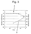
- Fig. 3 shows an LED relative efficiency and intensity variations (the ratio of minimum intensity to maximum intensity) of the foregoing semiconductor light emitting apparatus 10 when the height b of the reflector 13 is changed with respect to the size a of the LED chips 12.
- the LED relative efficiency indicates the light output efficiency of the LEDs. It drops gradually as the ratio of b/a increases,' i.e., the height b of the reflector 13 increases.
- intensity variations decrease as the value approaches 1.
- the ratio of b/a fall within the range of 1.0 to 2.0.
- a semiconductor light emitting apparatus of conventional structure was fabricated.
- the conventional apparatus was formed by filling a light transmitting resin containing a fluorescent material and a light diffusing material into a reflector so that the fluorescent material precipitated on the entire surfaces of the LED chips and the substrate and thermally curing the same.
- a semiconductor light emitting apparatus according to the exemplary embodiment of the present invention shown in Fig. 1 was fabricated. The semiconductor light emitting apparatuses were each measured for intensity and chromaticity' in the longitudinal direction, followed by normalization.
- the semiconductor light emitting apparatus 10 For intensity, as shown in Fig. 4 , the semiconductor light emitting apparatus 10 according to the exemplary embodiment of the present invention showed an intensity distribution characteristic shown by the solid line.
- the semiconductor light emitting apparatus of the conventional structure showed an intensity distribution characteristic shown by the dotted line.
- the semiconductor light emitting apparatus 10 suppresses intensity drops between the LED chips 12 by the scattering of light in the light diffusion layer 15.
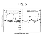
- the semiconductor light emitting apparatus 10 For chromaticity, as shown in Fig. 5 , the semiconductor light emitting apparatus 10 according to the exemplary embodiment of the present invention showed a chromaticity distribution characteristic shown by the solid line.
- the semiconductor light emitting apparatus of the conventional structure showed a chromaticity distribution characteristic shown by the dotted line.
- the semiconductor light emitting apparatus of the conventional structure causes chromaticity variations due to the light emitted from the fluorescent material that precipitated on the top of the substrate 11 around the LED chips 12.
- the semiconductor light emitting apparatus 10 according to the exemplary embodiment of the present invention suppresses chromaticity variations around the LED chips 12.
- Fig. 6 shows the configuration of a second exemplary embodiment of the semiconductor light emitting apparatus according to the present invention.
- the semiconductor light emitting apparatus 20 has almost the same configuration as that of the semiconductor light emitting device 10 shown in Figs. 1 and 2 .
- the only difference lies in the provision of a light diffusion sheet 21 which is arranged near the top of the reflector 13 and an inert gas 22 which is sealed in the recess 13a of the reflector 13, instead of the light diffusion layer 15.
- the light diffusion sheet 21 can be formed in the shape of a flat plate, for example, using frosted glass, opalescent glass, a silicone resin with a dispersed light-scattering material, or the like.
- the light diffusion sheet 21 may preferably be made of a material having heat resistance of approximately 300°C or above so as to allow a solder reflow mount process when mounting this semiconductor light emitting apparatus 20.
- the light'diffusion sheet 21 can be placed with its periphery on a step 13b which is formed around the top edge of the inner surface of the recess 13a in the reflector 13. It can be bonded to the step 13b, for example, with an epoxy adhesive, a silicone adhesive, a low-melting glass, or the like.
- the inert gas 22 can be made of nitrogen, argon gas, or the like, for example, and can be sealed in the recess 13a of the reflector 13 by a sealing step of bonding the periphery of the light diffusion sheet 21 to the step 13b of the reflector 13 to seal the interior of the recess 13a of the reflector 13.
- the inert gas 22 can be sealed into the recess 13a of the reflector 13 by preparing the interior of the sealing system in the inert gas atmosphere, or locally injecting the inert gas into the recess 13a of the reflector 13 from a gas supply nozzle or the like immediately before placing the light diffusion sheet 21 onto the step 13b of the reflector 13.
- the semiconductor light emitting apparatus 20 having such a configuration can provide almost the same operation as that of the semiconductor light emitting apparatus 10 shown in Figs. 1 and 2 .
- the mixed-color light emitted from the LED chips 12 into the recess 13a of the reflector 13 through the fluorescent material layer 14 (being a mixture of direct light emitted from the LED and fluorescence emitted from the fluorescent material) can be scattered by the light diffusion sheet 22 when emitted upward through the light diffusion sheet 22 directly or by reflection from the inner surface of the recess 13a of the reflector 13.
- the light to be emitted outside can be scattered as with the light diffusion layer 15 of the semiconductor light emitting apparatus 10 shown in Figs. 1 and 2 . This can consequently reduce color variations and intensity variations of the light emitted from the semiconductor light emitting apparatus 10.
- the LED chips 12 mounted in the recess 13a of the reflector 13 can be sealed in the recess 13a of the reflector 13 with the inert gas 22. This can provide protection against oxidation and the like.
- the foregoing exemplary embodiments have dealt with the cases of using the LED chips 12 as the semiconductor light emitting device chips.
Landscapes
- Led Device Packages (AREA)
Abstract
Description
- The present invention relates to a semiconductor light emitting apparatus which emits light from its semiconductor light emitting devices through a wavelength converting material and a light diffusing material.
- Conventionally, such semiconductor light emitting apparatuses have been disclosed, for example, in Japanese Patent No.
3,690,968 2001-077433 2006-165416 - More specifically, in Japanese Patent No.
3,690,968 - In this instance, the abovementioned fluorescent material has a specific gravity higher than those of the translucent mold member and the diffusing material. In the translucent mold member cured inside the cavity recess, it is possible to provide a concentration gradient of the fluorescent material. Accordingly, the fluorescent material increases in concentration as approaching the semiconductor light emitting device below. The light diffusing material increases in concentration as approaching the top of the translucent mold member above.
- According to the semiconductor light emitting apparatus having such a configuration, when the semiconductor light emitting device emits light, the light from the semiconductor light emitting device is incident on the fluorescent material to excite the fluorescent material. As a result, the fluorescent material emits fluorescence with a predetermined color, which is scattered by the light diffusing material and emitted outside from the surface of the translucent mold member.
- In this instance, the light diffusing material is configured to have a function of reflecting light from outside and a function of scattering fluorescence that is emitted from the fluorescent material when excited by the light emitted from the semiconductor light emitting device.
- On the other hand, the semiconductor light emitting apparatus disclosed in Japanese Patent Application Laid-Open No.
2006-165416 - By the way, in either of the semiconductor light emitting apparatuses disclosed in Japanese Patent No.
3,690,968 2006-165416 - Nevertheless, in the semiconductor light emitting apparatus disclosed in Japanese Patent No.
3,690,968 - For example, when a combination of a blue light emitting device and a yellow fluorescent material is used in this type of semiconductor light emitting apparatus for achieving white light, this configuration can result in more yellowish color, causing color variations in terms of the entire light emitting surface of the semiconductor light emitting apparatus.
- Because these areas are located around the light emitting device, the light emitted from the device cannot enter these areas easily. Accordingly, these areas are low in the intensity of excitation by the semiconductor light emitting device in spite of the high concentration of the fluorescent material. This lowers the intensity of the fluorescence, causing significant intensity variations in terms of the entire light emitting surface of the semiconductor light emitting apparatus.
- Moreover, if a diffusion sheet is overlaid on the light emitting surface of the foregoing semiconductor light emitting apparatus for the purpose of a backlight intended for a liquid crystal display, the color variations and the intensity variations mentioned above can be reduced comparatively. Nevertheless, when high-current power LEDs are used as the semiconductor light emitting device and built into the optical system of a reflector, projector, and the like, the foregoing color variations and intensity variations appear significantly to deteriorate the quality of the semiconductor light emitting apparatus as a light source.
- In the semiconductor light emitting apparatus disclosed in Japanese Patent Application Laid-Open No.
2006-165416 - In view of the foregoing, it is an object of the present invention to provide a semiconductor light emitting apparatus which can reduce color variations and intensity variations with a simple configuration.
- According to the present invention, a semiconductor light emitting apparatus can include: a substrate having a conductive member for making a chip mounting area and an electrode area; a semiconductor light emitting device chip mounted in the chip mounting area on this substrate; a reflector formed on this substrate so as to surround the semiconductor light emitting device chip; and a wavelength converting material and a light diffusing material arranged distributedly inside this reflector, wherein the semiconductor light emitting device chip emits light only from its top, and a first light transmitting resin containing the wavelength converting material is applied only to the surface of the semiconductor light emitting device chip. By the thus configured semiconductor light emitting apparatus, the foregoing and other objects have been achieved.
- In the semiconductor light emitting apparatus according to the present invention, the first light transmitting resin containing the wavelength converting material alone may preferably be coated and cured on the top of the semiconductor light emitting device chip so as to bulge upward because of surface tension.
- In the semiconductor light emitting apparatus according to the present invention, a second light transmitting resin containing the light diffusing material alone may preferably be filled into the reflector so as to cover the first light transmitting resin.
- In the semiconductor light emitting apparatus according to the present invention, the reflector preferably can have a step in an upper part of an inner surface thereof, and a light diffusion sheet containing the light diffusing material may preferably be placed on the step so as to cover an interior of a recess in the reflector.
- In the semiconductor light emitting apparatus according to the present invention, an inert gas may preferably be sealed in the recess of the reflector.
- In the semiconductor light emitting apparatus according to the present invention, the reflector may preferably have a height 1.0 to 2.0 times that of the semiconductor light emitting device chip.
- In the semiconductor light emitting apparatus according to the present invention, the wavelength converting material may preferably be a fluorescent material.
- According to the foregoing configuration, the semiconductor light emitting device chip can emit light when a drive voltage is applied to this semiconductor light emitting device chip through the conductive members on the substrate. The light emitted from the semiconductor light emitting device chip can be transmitted through the first light transmitting resin containing the wavelength converting material (or fluorescent material, hereinafter for simplicity) and emitted outside.
- On that occasion, part of the light emitted from the semiconductor light emitting device chip can impinge on the fluorescent material to excite the fluorescent material. As a result, the fluorescent material can emit fluorescence. The fluorescence from the fluorescent material may be mixed in color with the light emitted from the semiconductor light emitting device chip, and may be diffused further by the light diffusing material in the reflector. Consequently, the two can be well mixed in color and emitted outside.
- In this instance, the concentration of the fluorescent material in the first light transmitting resin applied to the top of the semiconductor light emitting device chip can be controlled easily, for example, by the amount of application of the first light transmitting resin to the top of the semiconductor light emitting device chip in a dispenser system or the like.
- Consequently, the mixed-color light can be made almost uniform in color, because the light emitted from the top of the semiconductor light emitting device chip excites the fluorescent material contained in the first light transmitting resin applied to the top immediately after emission in addition to the appropriate amount of contained fluorescent material. This can reduce the occurrence of color variations.
- In addition, this mixed-color light is sufficiently diffused by the light diffusing material which is arranged distributedly inside the reflector, and intensity variations can thus be reduced near the top of the reflector.
- In the above configuration, the semiconductor light emitting device chip can emit light only from its top and the first light transmitting resin containing the fluorescent material alone is cured on the top of the semiconductor light emitting device chip so as to bulge upward because of surface tension. Accordingly, the intensity of the light emitted from the semiconductor light emitting device chip can be allowed to be almost uniform with respect to the emission angle, and the concentration of the fluorescent material can be allowed to be almost uniform with respect to this light. This can further reduce the occurrence of color variations.
- When the second light transmitting resin containing the light diffusing material alone is filled into the reflector so as to cover the first light transmitting resin, the semiconductor light emitting device chip can be sealed and protected by this second light transmitting resin in the reflector, and the light diffusing material can be arranged distributedly inside the reflector.
- When the reflector has a step in the upper part of its inner surface, and a light diffusion sheet containing the light diffusing material is placed on this step so as to cover the interior of the recess in the reflector, it follows that a card of light diffusing material lies near the top of the reflector. Consequently, the light emitted from the semiconductor light emitting device chip can be scattered when it is transmitted through the light diffusion sheet near the external emission surface. This allows a reduction of intensity variations.
- When an inert gas is sealed in the recess of the reflector, the semiconductor light emitting device chip, even not sealed with a resin, can be surrounded by the inert gas in the reflector. This can prevent the semiconductor light emitting device chip from contact with air, thereby protecting it from oxidation and the like.
- When the reflector has a height 1.0 to 2.0 times that of the semiconductor light emitting device chip, intensity variations can be suppressed effectively at the light emitting surface at the top of the reflector without lowering the output efficiency of the light from the semiconductor light emitting device chip.
- As above, according to the present invention, the first light transmitting resin containing the fluorescent material alone can be applied only to the top of the semiconductor light emitting device chip while the light diffusing material can be arranged distributedly inside the reflector. This can reduce color variations and intensity variations of the mixed-color light emitted upward from the top of the reflector, thereby providing uniform plane emission which is suitable for, for example, a surface light source.
- These and other characteristics, features, and advantages of the presently disclosed subject matter will become clear from the following description with reference to the accompanying drawings, wherein:
-
Fig. 1 is a schematic cross-sectional view showing the configuration of a first exemplary embodiment of the semiconductor light emitting apparatus according to the present invention; -
Fig. 2 is a schematic plan view of the semiconductor light emitting apparatus ofFig. 1 ; -
Fig. 3 is a graph showing an LED relative efficiency and intensity variations of the semiconductor light emitting apparatus ofFig. 1 when the ratio between the size of the LED chips and the height of the reflector is changed; -
Fig. 4 is a graph showing measurements on the intensity distribution in the longitudinal direction of the semiconductor light emitting apparatus ofFig. 1 ; -
Fig. 5 is a graph showing measurements on the chromaticity distribution in the longitudinal direction of the semiconductor light emitting apparatus ofFig. 1 ; and -
Fig. 6 is a schematic sectional diagram showing the configuration of a second exemplary embodiment of the semiconductor light emitting apparatus according to the present invention. - Hereinafter, preferred exemplary embodiments of the present invention will be described in detail with reference to
Figs. 1 to 6 . -
Figs. 1 and 2 show the configuration of a first exemplary embodiment of the semiconductor light emitting apparatus according to the present invention. - In
Figs. 1 and 2 , the semiconductorlight emitting apparatus 10 can be configured to include: asubstrate 11; a plurality (four, in the shown case) of LED chips 12 as semiconductor light emitting device chips mounted'on thesubstrate 11; a frame-shapedreflector 13 which is formed on thesubstrate 11 so as to surround these LED chips 12; a wavelength converting material layer orfluorescent material layer 14 arranged on the top of each LED chip 12; and alight diffusion layer 15 containing a light diffusing material and arranged in a recess 13a of thereflector 13. - The
substrate 11 can be a flat wiring board made of a material having high thermal conductivity, such as aluminum oxide, aluminum nitride, silicon carbide, silicon nitride, zirconium oxide, or silicon. Conductive patterns can be formed on the surface and/or inside as conductive members. - As shown in
Fig. 2 , these conductive patterns can include: chip mounting areas 16a and electrode areas 17a at the tops of their extremities; and surface-mounting terminal portions (not shown) which are extended from those areas to the top or bottom via both side edges. - The foregoing LED chips 12 are preferably formed by depositing a PN semiconductor layer on a nontransparent substrate, for example. The LED chips 12 can have light emitting surfaces at their tops alone, not emitting light from the chip sides.
- The LED chips 12 can be bonded onto the chip mounting areas 16a of the one conductive pattern of the
substrate 11 by die-bonding or the like, using a bonding material such as an Au-Sn alloy, Pb-free solder, or an Ag paste. Electrode areas at their surfaces can also be electrically connected to the electrode areas 17a of the other conductive pattern by wire bonding with gold wires or the like. - The
reflector 13 can have a recess 13a which is formed to surround the periphery of the LED chips 12 with its inner surface tilted to spread out upward. - The
reflector 13 can be made of a material having high reflectivity, or alternatively the inner surface of the recess 13a is plated with a material having high reflectivity as a reflecting surface. - The
fluorescent material layer 14 can be formed by mixing particles of fluorescent material 14a into a light transmitting resin such as epoxy resin. It is applied to the tops of the LED chips 12 using a general-purpose dispenser system or the like, followed by curing. - The fluorescent material serving as a wavelength converting material may be formed of ZnS:Cu, SiAlON:Eu, or Ca3Sc2(SiO4)3:Ce.
- In this case, the LED chips 12 can be shaped by mechanical dicing, laser scribing, or the like, typically in a fine processing step on a wafer so as to form right-angled edges of the chips 12. The
fluorescent material layer 14 applied to the tops of these LED chips 12 is thus formed to bulge out thickly because of the surface tension of the light transmitting resin. - In this instance, LED chips are increasing in size with increasing LED currents in recent years. With chip sizes of a 1-mm square or so, it is therefore sufficiently possible to apply the fluorescent material layer in a quantitative fashion using a dispenser system.
- The
light diffusion layer 15 can be formed by mixing a light diffusing material into a light transmitting resin such as epoxy resin. It can be filled into the recess 13a of thereflector 13 and cured by heating, for example. - In this instance, the light diffusing material can be made of a material having a refractive index different from that of the light transmitting resin, such as fine powders of silicon oxide, aluminum oxide, titanium oxide, or silicone beads.
- The semiconductor
light emitting apparatus 10 according to the present embodiment of the present invention can be configured as described above. The LED chips 12 can emit light when a drive voltage is applied to the respective LED chips 12 through the pair of conductive patterns. - The light emitted from the top of each LED chip 12 can be incident on the
fluorescent material layer 14, and part of it can impinge on the particles of the fluorescent material 14a in thefluorescent material layer 14 to excite the fluorescent material. - As a result, the fluorescent material can emit fluorescence, which is mixed with the light directly from each LED chip 12 in color and enter from the
fluorescent material layer 14 into thelight diffusion layer 15. - In this case, the light emitted from each LED chip 12 can be incident on the
fluorescent material layer 14 immediately after emission, excite the fluorescent material 14a, and make the fluorescent material 14a emit fluorescence. - The
fluorescent material layer 14 can be thickly formed by surface tension in accordance with the present invention. This can provide a sufficient concentration of fluorescent material corresponding to the light emitted from each LED chip 12. This also makes the amount of fluorescence emitted from the fluorescent material 14a sufficient. - Moreover, the fluorescent material 14a lies in the
fluorescent material layer 14 alone, not in thelight diffusion layer 15. This can reduce the occurrence of color variations. - In this way, the mixed-color light incident on the light diffusion layer 15 (being a mixture of direct light emitted from the LED and fluorescence emitted from the fluorescent material) can be emitted directly or sideways, reflected from the inner surface of the recess 13a in the
reflector 13, and then emitted outside from the top of thelight diffusion layer 15. - On that occasion, part of the mixed-color light incident on the
light diffusion layer 15 can impinge on the particles of the light diffusing material in thelight diffusion layer 15 to scatter. The mixed-color light can thus be diffused sufficiently in thelight diffusion layer 15 before emitted outside from the top of thelight diffusion layer 15. - As a result, the light emitted outside from the top of this
light diffusion layer 15 can fully cover the areas between the individual LED chips 12 because of the diffusion by thelight diffusion layer 15, thereby suppressing a partial drop in intensity in the semiconductorlight emitting apparatus 10. - In this way, variations in the intensity of the light emitted from the top of the
light diffusion layer 15 can be efficiently reduced. Furthermore, such scattering can also reduce color variations further. -
Fig. 3 shows an LED relative efficiency and intensity variations (the ratio of minimum intensity to maximum intensity) of the foregoing semiconductorlight emitting apparatus 10 when the height b of thereflector 13 is changed with respect to the size a of the LED chips 12. - As shown by the reference symbol A, the LED relative efficiency indicates the light output efficiency of the LEDs. It drops gradually as the ratio of b/a increases,' i.e., the height b of the
reflector 13 increases. - In contrast, intensity variations decrease as the value approaches 1. The greater the height b of the reflector is, the closer the intensity variations approach to 1.
- In order to suppress intensity variations without lowering the LED relative efficiency, it is therefore desirable that the ratio of b/a fall within the range of 1.0 to 2.0.
- A description will now be given of experiments for measuring the foregoing semiconductor
light emitting apparatus 10 for intensity and chromaticity in its longitudinal direction (the direction shown by the dotted line X inFig. 2 ). - Initially, using LED chips 12 having a size a of 1 mm and a
reflector 13 having a height b of 1.5 mm, a semiconductor light emitting apparatus of conventional structure was fabricated. The conventional apparatus was formed by filling a light transmitting resin containing a fluorescent material and a light diffusing material into a reflector so that the fluorescent material precipitated on the entire surfaces of the LED chips and the substrate and thermally curing the same. Furthermore, a semiconductor light emitting apparatus according to the exemplary embodiment of the present invention shown inFig. 1 was fabricated. The semiconductor light emitting apparatuses were each measured for intensity and chromaticity' in the longitudinal direction, followed by normalization. - For intensity, as shown in
Fig. 4 , the semiconductorlight emitting apparatus 10 according to the exemplary embodiment of the present invention showed an intensity distribution characteristic shown by the solid line. The semiconductor light emitting apparatus of the conventional structure showed an intensity distribution characteristic shown by the dotted line. - Then, as compared to the semiconductor light emitting apparatus of the conventional structure, it is seen that the semiconductor
light emitting apparatus 10 according to the exemplary embodiment of the present invention suppresses intensity drops between the LED chips 12 by the scattering of light in thelight diffusion layer 15. - For chromaticity, as shown in
Fig. 5 , the semiconductorlight emitting apparatus 10 according to the exemplary embodiment of the present invention showed a chromaticity distribution characteristic shown by the solid line. The semiconductor light emitting apparatus of the conventional structure showed a chromaticity distribution characteristic shown by the dotted line. - It can thus be seen that the semiconductor light emitting apparatus of the conventional structure causes chromaticity variations due to the light emitted from the fluorescent material that precipitated on the top of the
substrate 11 around the LED chips 12. In contrast, the semiconductorlight emitting apparatus 10 according to the exemplary embodiment of the present invention suppresses chromaticity variations around the LED chips 12. -
Fig. 6 shows the configuration of a second exemplary embodiment of the semiconductor light emitting apparatus according to the present invention. - In
Fig. 6 , the semiconductorlight emitting apparatus 20 has almost the same configuration as that of the semiconductorlight emitting device 10 shown inFigs. 1 and 2 . The only difference lies in the provision of alight diffusion sheet 21 which is arranged near the top of thereflector 13 and aninert gas 22 which is sealed in the recess 13a of thereflector 13, instead of thelight diffusion layer 15. - In this instance, the
light diffusion sheet 21 can be formed in the shape of a flat plate, for example, using frosted glass, opalescent glass, a silicone resin with a dispersed light-scattering material, or the like. - It should be appreciated that the
light diffusion sheet 21 may preferably be made of a material having heat resistance of approximately 300°C or above so as to allow a solder reflow mount process when mounting this semiconductorlight emitting apparatus 20. - The
light'diffusion sheet 21 can be placed with its periphery on astep 13b which is formed around the top edge of the inner surface of the recess 13a in thereflector 13. It can be bonded to thestep 13b, for example, with an epoxy adhesive, a silicone adhesive, a low-melting glass, or the like. - The
inert gas 22 can be made of nitrogen, argon gas, or the like, for example, and can be sealed in the recess 13a of thereflector 13 by a sealing step of bonding the periphery of thelight diffusion sheet 21 to thestep 13b of thereflector 13 to seal the interior of the recess 13a of thereflector 13. - In this case, the
inert gas 22 can be sealed into the recess 13a of thereflector 13 by preparing the interior of the sealing system in the inert gas atmosphere, or locally injecting the inert gas into the recess 13a of thereflector 13 from a gas supply nozzle or the like immediately before placing thelight diffusion sheet 21 onto thestep 13b of thereflector 13. - The semiconductor
light emitting apparatus 20 having such a configuration can provide almost the same operation as that of the semiconductorlight emitting apparatus 10 shown inFigs. 1 and 2 . In addition to this, the mixed-color light emitted from the LED chips 12 into the recess 13a of thereflector 13 through the fluorescent material layer 14 (being a mixture of direct light emitted from the LED and fluorescence emitted from the fluorescent material) can be scattered by thelight diffusion sheet 22 when emitted upward through thelight diffusion sheet 22 directly or by reflection from the inner surface of the recess 13a of thereflector 13. - As a result, the light to be emitted outside can be scattered as with the
light diffusion layer 15 of the semiconductorlight emitting apparatus 10 shown inFigs. 1 and 2 . This can consequently reduce color variations and intensity variations of the light emitted from the semiconductorlight emitting apparatus 10. - Moreover, the LED chips 12 mounted in the recess 13a of the
reflector 13 can be sealed in the recess 13a of thereflector 13 with theinert gas 22. This can provide protection against oxidation and the like. - The foregoing exemplary embodiments have dealt with the cases where four LED chips 12 are arranged in line inside the
reflector 13. This is not restrictive, however, and it is understood that one to three LED chips 12 or more than four may be provided. - Moreover, the foregoing exemplary embodiments have dealt with the cases of using the LED chips 12 as the semiconductor light emitting device chips. This is not restrictive, however, and other types of semiconductor light emitting device chips such as a semiconductor laser device chip may also be used.
- As above, according to the present invention, it is possible to provide a superexcellent semiconductor light emitting apparatus which can reduce color variations and intensity variations with a simple configuration.
Claims (14)
- A semiconductor light emitting apparatus (10, 20) comprising:a substrate (11) having a conductive member for making a chip mounting area (16a) and an electrode area (17a);a semiconductor light emitting device chip (12) mounted in the chip mounting area (16a) on the substrate (11);a reflector (13) formed on the substrate (11) so as to surround the semiconductor light emitting device chip (12); anda wavelength converting material (14a) and a light diffusing material arranged distributedly inside the reflector (13), whereinthe semiconductor light emitting device chip (12) emits light only from its top, anda first light transmitting resin (14) containing the wavelength converting material (14a) is applied only to the top of the semiconductor light emitting device chip (12).
- The semiconductor light emitting apparatus (10, 20) according to claim 1, wherein the first light transmitting resin (14) containing the wavelength converting material (14a) alone is coated and cured on the top of the semiconductor light emitting device chip (12) so as to bulge upward because of surface tension.
- The semiconductor light emitting apparatus (10, 20) according to claim 2, wherein a second light transmitting resin containing the light diffusing material alone is filled into the reflector (13) so as to cover the first light transmitting resin (14).
- The semiconductor light emitting apparatus (20) according to any one of claims 1 to 3, wherein:the reflector (13) has a step (13b) in an upper part of an inner surface thereof; anda light diffusion sheet (21) including the light diffusing material is placed on the step (13b) so as to cover an interior of a recess (13a) in the reflector (13).
- The semiconductor light emitting apparatus (20) according to claim 4, wherein an inert gas is sealed in the recess (13a) of the reflector (13).
- The semiconductor light emitting apparatus (10, 20) according to any one of claims 1 to 5, wherein the reflector (13) has a height 1.0 to 2.0 times that of the semiconductor light emitting device chip (12).
- The semiconductor light emitting apparatus (10, 20) according to any one of claims 1 to 6, wherein the wavelength converting material (14a) is a fluorescent material.
- A semiconductor light emitting apparatus (10, 20) comprising:a substrate (11);a semiconductor light emitting device chip (12) mounted on the substrate (11);a reflector (13) formed on the substrate (11) so as to surround the semiconductor light emitting device chip (12);a first light transmitting resin (14) containing a wavelength converting material (14a) provided to a top of the semiconductor light emitting device chip (12); anda transparent member (15, 21) containing a light diffusing material alone so as to cover the first light transmitting resin (14).
- The semiconductor light emitting apparatus (10, 20) according to claim 8, wherein the semiconductor light emitting device chip (12) emits light only from the top.
- The semiconductor light emitting apparatus (10, 20) according to claim 8 or 9, wherein the transparent member (15) is formed by filling a second light transmitting resin containing the light diffusing material alone into the reflector (13) so as to cover the first light transmitting resin (14).
- The semiconductor light emitting apparatus (20) according to any one of claims 8 to 10, wherein:the reflector (13) has a step (13b) in an upper part of an inner surface thereof; andthe transparent member includes a light diffusion sheet (21) including the light diffusing material placed on the step (13b) so as to cover an interior of a recess (13a) in the reflector (13).
- The semiconductor light emitting apparatus (20) according to claim 11, wherein an inert gas is sealed in the recess (13a) of the reflector (13).
- The semiconductor light emitting apparatus (10, 20) according to any one of claims 8 to 12, wherein the reflector (13) has a height 1.0 to 2.0 times that of the semiconductor light emitting device chip (12).
- The semiconductor light emitting apparatus (10, 20) according to any one of claims 8 to 13, wherein the wavelength converting material (14a) is a fluorescent material.
Applications Claiming Priority (1)
| Application Number | Priority Date | Filing Date | Title |
|---|---|---|---|
| JP2007049511A JP5013905B2 (en) | 2007-02-28 | 2007-02-28 | Semiconductor light emitting device |
Publications (2)
| Publication Number | Publication Date |
|---|---|
| EP1965445A2 true EP1965445A2 (en) | 2008-09-03 |
| EP1965445A3 EP1965445A3 (en) | 2013-04-03 |
Family
ID=39472608
Family Applications (1)
| Application Number | Title | Priority Date | Filing Date |
|---|---|---|---|
| EP08002751A Withdrawn EP1965445A3 (en) | 2007-02-28 | 2008-02-14 | Semiconductor light emitting apparatus |
Country Status (3)
| Country | Link |
|---|---|
| US (1) | US7926973B2 (en) |
| EP (1) | EP1965445A3 (en) |
| JP (1) | JP5013905B2 (en) |
Cited By (2)
| Publication number | Priority date | Publication date | Assignee | Title |
|---|---|---|---|---|
| WO2013104606A1 (en) * | 2012-01-11 | 2013-07-18 | Osram Gmbh | Optoelectronic component with inert gas atmosphere |
| EP2479812A3 (en) * | 2011-01-24 | 2014-08-27 | Stanley Electric Co., Ltd. | Semiconductor light emitting device and manufacturing method |
Families Citing this family (22)
| Publication number | Priority date | Publication date | Assignee | Title |
|---|---|---|---|---|
| TWI499076B (en) * | 2008-07-03 | 2015-09-01 | 三星電子股份有限公司 | Wavelength-converting LED chip and light-emitting device including the same |
| US7919339B2 (en) * | 2008-09-08 | 2011-04-05 | Iledm Photoelectronics, Inc. | Packaging method for light emitting diode module that includes fabricating frame around substrate |
| JP5227135B2 (en) * | 2008-10-10 | 2013-07-03 | スタンレー電気株式会社 | Semiconductor light emitting device and manufacturing method thereof |
| WO2010134331A1 (en) * | 2009-05-22 | 2010-11-25 | Panasonic Corporation | Semiconductor light-emitting device and light source device using the same |
| JP5431232B2 (en) * | 2010-03-31 | 2014-03-05 | 三洋電機株式会社 | Semiconductor device |
| WO2011125885A1 (en) * | 2010-03-31 | 2011-10-13 | インテックス株式会社 | Light-source device |
| KR101115460B1 (en) * | 2010-04-02 | 2012-02-24 | (주) 아모엘이디 | LED package |
| EP2378576A2 (en) * | 2010-04-15 | 2011-10-19 | Samsung LED Co., Ltd. | Light emitting diode package, lighting apparatus having the same, and method for manufacturing light emitting diode package |
| TWI561770B (en) * | 2010-04-30 | 2016-12-11 | Samsung Electronics Co Ltd | Light emitting device package, light source module, backlight unit, display apparatus, television set, and illumination apparatus |
| US8654064B2 (en) * | 2010-10-18 | 2014-02-18 | Samsung Display Co., Ltd. | Backlight having blue light emitting diodes and method of driving same |
| JP2013004739A (en) * | 2011-06-16 | 2013-01-07 | Panasonic Corp | Light-emitting device and lighting equipment using the same |
| KR101945532B1 (en) | 2011-08-16 | 2019-02-07 | 루미리즈 홀딩 비.브이. | Led mixing chamber with reflective walls formed in slots |
| JP2013080833A (en) * | 2011-10-04 | 2013-05-02 | Stanley Electric Co Ltd | Light emitting device and manufacturing method of the same |
| DE102012109806A1 (en) * | 2012-10-15 | 2014-04-17 | Osram Opto Semiconductors Gmbh | Radiation-emitting component |
| US9761763B2 (en) * | 2012-12-21 | 2017-09-12 | Soraa, Inc. | Dense-luminescent-materials-coated violet LEDs |
| JP2014130963A (en) * | 2012-12-28 | 2014-07-10 | Nichia Chem Ind Ltd | Light emitting device |
| US9728685B2 (en) * | 2013-02-28 | 2017-08-08 | Nichia Corporation | Light emitting device and lighting device including same |
| JP6172455B2 (en) * | 2013-10-07 | 2017-08-02 | 豊田合成株式会社 | Light emitting device |
| JP2016076634A (en) * | 2014-10-08 | 2016-05-12 | エルジー ディスプレイ カンパニー リミテッド | Led package, backlight unit, and liquid crystal display device |
| JP6278035B2 (en) * | 2015-11-27 | 2018-02-14 | 日亜化学工業株式会社 | Method for manufacturing light emitting device |
| CN107093658A (en) * | 2016-09-30 | 2017-08-25 | 深圳市玲涛光电科技有限公司 | Light-emitting component, backlight source module and electronic equipment |
| JP7007589B2 (en) * | 2018-07-24 | 2022-01-24 | 日亜化学工業株式会社 | Luminescent device |
Citations (6)
| Publication number | Priority date | Publication date | Assignee | Title |
|---|---|---|---|---|
| WO1997050132A1 (en) | 1996-06-26 | 1997-12-31 | Siemens Aktiengesellschaft | Light-emitting semiconductor component with luminescence conversion element |
| WO1998012757A1 (en) | 1996-09-20 | 1998-03-26 | Siemens Aktiengesellschaft | Sealing material with wavelength converting effect, application and production process |
| US20040096998A1 (en) * | 2002-11-19 | 2004-05-20 | United Epitaxy Company Ltd | Method for manufacturing light-emitting element on non-transparent substrate |
| US20050205876A1 (en) | 2004-03-22 | 2005-09-22 | Mitsunori Harada | Semiconductor light-emitting device and method of fabricating the same |
| JP2005340472A (en) | 2004-05-26 | 2005-12-08 | Kyocera Corp | Light emitting device and lighting device |
| DE102004036157A1 (en) | 2004-07-26 | 2006-02-16 | Osram Opto Semiconductors Gmbh | Electromagnetic radiation emitting optoelectronic component and light module |
Family Cites Families (15)
| Publication number | Priority date | Publication date | Assignee | Title |
|---|---|---|---|---|
| JP4171107B2 (en) * | 1998-07-09 | 2008-10-22 | スタンレー電気株式会社 | Planar light source |
| JP3690968B2 (en) | 1999-06-30 | 2005-08-31 | 日亜化学工業株式会社 | LIGHT EMITTING DEVICE AND METHOD FOR FORMING THE SAME |
| DE20115914U1 (en) * | 2001-09-27 | 2003-02-13 | Patent-Treuhand-Gesellschaft für elektrische Glühlampen mbH, 81543 München | Lighting unit with at least one LED as a light source |
| US7070804B2 (en) * | 2001-10-23 | 2006-07-04 | Boehringer Ingelheim International Gmbh | Chewable tablet containing lysine |
| JP3702863B2 (en) * | 2002-05-15 | 2005-10-05 | 住友電気工業株式会社 | White light emitting device |
| JP2004362887A (en) * | 2003-06-03 | 2004-12-24 | Yamaha Livingtec Corp | Lighting system |
| US7088038B2 (en) * | 2003-07-02 | 2006-08-08 | Gelcore Llc | Green phosphor for general illumination applications |
| JP4622253B2 (en) * | 2004-01-22 | 2011-02-02 | 日亜化学工業株式会社 | Light emitting device and manufacturing method thereof |
| JP5320655B2 (en) * | 2004-06-30 | 2013-10-23 | 三菱化学株式会社 | LIGHT EMITTING DEVICE, LIGHTING, BACKLIGHT UNIT FOR DISPLAY DEVICE, AND DISPLAY DEVICE |
| JP4389126B2 (en) * | 2004-10-04 | 2009-12-24 | スタンレー電気株式会社 | Semiconductor light emitting device and manufacturing method thereof |
| JP2006165416A (en) | 2004-12-10 | 2006-06-22 | Stanley Electric Co Ltd | White display and manufacturing method thereof |
| WO2006067885A1 (en) * | 2004-12-24 | 2006-06-29 | Kyocera Corporation | Light-emitting device and illuminating device |
| JP2006253229A (en) * | 2005-03-08 | 2006-09-21 | Toyoda Gosei Co Ltd | Led light emitting device, and method of forming reflector used therefor |
| JP2007018936A (en) * | 2005-07-08 | 2007-01-25 | Toyoda Gosei Co Ltd | Light source device |
| JP4715422B2 (en) * | 2005-09-27 | 2011-07-06 | 日亜化学工業株式会社 | Light emitting device |
-
2007
- 2007-02-28 JP JP2007049511A patent/JP5013905B2/en not_active Expired - Fee Related
-
2008
- 2008-02-14 EP EP08002751A patent/EP1965445A3/en not_active Withdrawn
- 2008-02-25 US US12/036,556 patent/US7926973B2/en not_active Expired - Fee Related
Patent Citations (6)
| Publication number | Priority date | Publication date | Assignee | Title |
|---|---|---|---|---|
| WO1997050132A1 (en) | 1996-06-26 | 1997-12-31 | Siemens Aktiengesellschaft | Light-emitting semiconductor component with luminescence conversion element |
| WO1998012757A1 (en) | 1996-09-20 | 1998-03-26 | Siemens Aktiengesellschaft | Sealing material with wavelength converting effect, application and production process |
| US20040096998A1 (en) * | 2002-11-19 | 2004-05-20 | United Epitaxy Company Ltd | Method for manufacturing light-emitting element on non-transparent substrate |
| US20050205876A1 (en) | 2004-03-22 | 2005-09-22 | Mitsunori Harada | Semiconductor light-emitting device and method of fabricating the same |
| JP2005340472A (en) | 2004-05-26 | 2005-12-08 | Kyocera Corp | Light emitting device and lighting device |
| DE102004036157A1 (en) | 2004-07-26 | 2006-02-16 | Osram Opto Semiconductors Gmbh | Electromagnetic radiation emitting optoelectronic component and light module |
Cited By (4)
| Publication number | Priority date | Publication date | Assignee | Title |
|---|---|---|---|---|
| EP2479812A3 (en) * | 2011-01-24 | 2014-08-27 | Stanley Electric Co., Ltd. | Semiconductor light emitting device and manufacturing method |
| WO2013104606A1 (en) * | 2012-01-11 | 2013-07-18 | Osram Gmbh | Optoelectronic component with inert gas atmosphere |
| US9640739B2 (en) | 2012-01-11 | 2017-05-02 | Osram Gmbh | Optoelectronic component with inert gas atmosphere |
| DE102012200327B4 (en) | 2012-01-11 | 2022-01-05 | Osram Gmbh | Optoelectronic component |
Also Published As
| Publication number | Publication date |
|---|---|
| US20080203419A1 (en) | 2008-08-28 |
| US7926973B2 (en) | 2011-04-19 |
| JP2008218460A (en) | 2008-09-18 |
| EP1965445A3 (en) | 2013-04-03 |
| JP5013905B2 (en) | 2012-08-29 |
Similar Documents
| Publication | Publication Date | Title |
|---|---|---|
| US7926973B2 (en) | Semiconductor light emitting apparatus | |
| JP5140082B2 (en) | Light emitting device | |
| US8922118B2 (en) | Light-emitting device | |
| JP5196711B2 (en) | LIGHT EMITTING DEVICE AND LIGHTING DEVICE USING THE SAME | |
| US10734556B2 (en) | Manufacturing method for light emitting device | |
| US7943953B2 (en) | Light emitting device and light emitting module | |
| EP2448028A2 (en) | Light emitting apparatus and production method thereof | |
| KR20050041986A (en) | Package for housing light-emitting element, light-emitting apparatus and illumination apparatus | |
| EP2017892A2 (en) | Light emitting device and method of manufacturing the same | |
| JP2017117912A (en) | Light emitting device using wavelength converting member, and wavelength converting member and method for manufacturing light emitting device | |
| JP5224890B2 (en) | Light emitting device and method for manufacturing light emitting device | |
| US9812495B2 (en) | Light emitting device and lighting apparatus | |
| TWI566437B (en) | Light emitting device and method of manufacturing same | |
| US10274667B2 (en) | Light-emitting device with two green light-emitting elements with different peak wavelengths and backlight including light-emitting device | |
| US20190198719A1 (en) | Light emitting device, light source device, and display device | |
| KR20190038424A (en) | Light-emitting device | |
| CN102222749A (en) | Light emitting component and module thereof | |
| JP2006093399A (en) | LIGHT EMITTING DEVICE, ITS MANUFACTURING METHOD, AND LIGHTING DEVICE | |
| TW201044651A (en) | Semiconductor light emitting device | |
| CN117790485A (en) | Method for manufacturing light emitting device and light emitting device | |
| CN105428511A (en) | Semiconductor light emitting device and lead frame | |
| JP4948841B2 (en) | Light emitting device and lighting device | |
| JP2016063210A (en) | Semiconductor light-emitting device and lead frame | |
| KR20120045539A (en) | Light emitting device package | |
| US12292651B2 (en) | Planar light source and liquid crystal display device |
Legal Events
| Date | Code | Title | Description |
|---|---|---|---|
| PUAI | Public reference made under article 153(3) epc to a published international application that has entered the european phase |
Free format text: ORIGINAL CODE: 0009012 |
|
| AK | Designated contracting states |
Kind code of ref document: A2 Designated state(s): AT BE BG CH CY CZ DE DK EE ES FI FR GB GR HR HU IE IS IT LI LT LU LV MC MT NL NO PL PT RO SE SI SK TR |
|
| AX | Request for extension of the european patent |
Extension state: AL BA MK RS |
|
| PUAL | Search report despatched |
Free format text: ORIGINAL CODE: 0009013 |
|
| AK | Designated contracting states |
Kind code of ref document: A3 Designated state(s): AT BE BG CH CY CZ DE DK EE ES FI FR GB GR HR HU IE IS IT LI LT LU LV MC MT NL NO PL PT RO SE SI SK TR |
|
| AX | Request for extension of the european patent |
Extension state: AL BA MK RS |
|
| RIC1 | Information provided on ipc code assigned before grant |
Ipc: H01L 33/00 20100101ALI20130227BHEP Ipc: H01L 25/075 20060101AFI20130227BHEP |
|
| 17P | Request for examination filed |
Effective date: 20131004 |
|
| RBV | Designated contracting states (corrected) |
Designated state(s): AT BE BG CH CY CZ DE DK EE ES FI FR GB GR HR HU IE IS IT LI LT LU LV MC MT NL NO PL PT RO SE SI SK TR |
|
| AKX | Designation fees paid |
Designated state(s): DE FR GB |
|
| 17Q | First examination report despatched |
Effective date: 20180123 |
|
| STAA | Information on the status of an ep patent application or granted ep patent |
Free format text: STATUS: THE APPLICATION HAS BEEN WITHDRAWN |
|
| 18W | Application withdrawn |
Effective date: 20180508 |