EP1964091B1 - Oled display with improved power performance - Google Patents
Oled display with improved power performance Download PDFInfo
- Publication number
- EP1964091B1 EP1964091B1 EP06839049.1A EP06839049A EP1964091B1 EP 1964091 B1 EP1964091 B1 EP 1964091B1 EP 06839049 A EP06839049 A EP 06839049A EP 1964091 B1 EP1964091 B1 EP 1964091B1
- Authority
- EP
- European Patent Office
- Prior art keywords
- pixel
- gamut
- luminance
- pixels
- display
- Prior art date
- Legal status (The legal status is an assumption and is not a legal conclusion. Google has not performed a legal analysis and makes no representation as to the accuracy of the status listed.)
- Active
Links
- 235000019557 luminance Nutrition 0.000 claims description 143
- 239000011159 matrix material Substances 0.000 claims description 27
- 238000000034 method Methods 0.000 claims description 24
- 230000002829 reductive effect Effects 0.000 claims description 16
- 230000033228 biological regulation Effects 0.000 claims description 12
- 230000001105 regulatory effect Effects 0.000 claims description 10
- 238000013507 mapping Methods 0.000 claims description 5
- 230000004044 response Effects 0.000 claims description 3
- 230000004913 activation Effects 0.000 claims 1
- 239000010410 layer Substances 0.000 description 59
- 239000003086 colorant Substances 0.000 description 30
- 230000006835 compression Effects 0.000 description 18
- 238000007906 compression Methods 0.000 description 18
- 239000003990 capacitor Substances 0.000 description 15
- 239000004065 semiconductor Substances 0.000 description 15
- 238000003860 storage Methods 0.000 description 11
- 230000007704 transition Effects 0.000 description 10
- 230000006870 function Effects 0.000 description 9
- 239000000463 material Substances 0.000 description 9
- 238000006243 chemical reaction Methods 0.000 description 8
- 230000008901 benefit Effects 0.000 description 7
- 238000010586 diagram Methods 0.000 description 7
- 230000007935 neutral effect Effects 0.000 description 7
- 239000004020 conductor Substances 0.000 description 6
- 230000006872 improvement Effects 0.000 description 6
- 239000000758 substrate Substances 0.000 description 6
- 229920001621 AMOLED Polymers 0.000 description 5
- 238000010276 construction Methods 0.000 description 5
- 230000000694 effects Effects 0.000 description 5
- 238000012805 post-processing Methods 0.000 description 5
- 230000009467 reduction Effects 0.000 description 5
- 239000000945 filler Substances 0.000 description 4
- 230000000670 limiting effect Effects 0.000 description 4
- 238000012886 linear function Methods 0.000 description 4
- 238000007781 pre-processing Methods 0.000 description 4
- 238000004321 preservation Methods 0.000 description 4
- 239000000243 solution Substances 0.000 description 4
- 229910052581 Si3N4 Inorganic materials 0.000 description 3
- 230000003213 activating effect Effects 0.000 description 3
- 238000013459 approach Methods 0.000 description 3
- 238000013461 design Methods 0.000 description 3
- 238000002347 injection Methods 0.000 description 3
- 239000007924 injection Substances 0.000 description 3
- 229910052751 metal Inorganic materials 0.000 description 3
- 239000002184 metal Substances 0.000 description 3
- 239000000203 mixture Substances 0.000 description 3
- 238000010606 normalization Methods 0.000 description 3
- HQVNEWCFYHHQES-UHFFFAOYSA-N silicon nitride Chemical compound N12[Si]34N5[Si]62N3[Si]51N64 HQVNEWCFYHHQES-UHFFFAOYSA-N 0.000 description 3
- 229910052709 silver Inorganic materials 0.000 description 3
- 239000004332 silver Substances 0.000 description 3
- XKRFYHLGVUSROY-UHFFFAOYSA-N Argon Chemical compound [Ar] XKRFYHLGVUSROY-UHFFFAOYSA-N 0.000 description 2
- IJGRMHOSHXDMSA-UHFFFAOYSA-N Atomic nitrogen Chemical compound N#N IJGRMHOSHXDMSA-UHFFFAOYSA-N 0.000 description 2
- VYPSYNLAJGMNEJ-UHFFFAOYSA-N Silicium dioxide Chemical compound O=[Si]=O VYPSYNLAJGMNEJ-UHFFFAOYSA-N 0.000 description 2
- 239000000654 additive Substances 0.000 description 2
- 230000000996 additive effect Effects 0.000 description 2
- 229910052782 aluminium Inorganic materials 0.000 description 2
- XAGFODPZIPBFFR-UHFFFAOYSA-N aluminium Chemical compound [Al] XAGFODPZIPBFFR-UHFFFAOYSA-N 0.000 description 2
- OSGAYBCDTDRGGQ-UHFFFAOYSA-L calcium sulfate Chemical compound [Ca+2].[O-]S([O-])(=O)=O OSGAYBCDTDRGGQ-UHFFFAOYSA-L 0.000 description 2
- 230000001276 controlling effect Effects 0.000 description 2
- 238000012888 cubic function Methods 0.000 description 2
- 230000007547 defect Effects 0.000 description 2
- 230000001419 dependent effect Effects 0.000 description 2
- 238000009826 distribution Methods 0.000 description 2
- 238000005538 encapsulation Methods 0.000 description 2
- AMGQUBHHOARCQH-UHFFFAOYSA-N indium;oxotin Chemical compound [In].[Sn]=O AMGQUBHHOARCQH-UHFFFAOYSA-N 0.000 description 2
- 239000012212 insulator Substances 0.000 description 2
- 238000004519 manufacturing process Methods 0.000 description 2
- 238000000059 patterning Methods 0.000 description 2
- 230000008569 process Effects 0.000 description 2
- 230000003595 spectral effect Effects 0.000 description 2
- 230000001629 suppression Effects 0.000 description 2
- 229910001316 Ag alloy Inorganic materials 0.000 description 1
- WHXSMMKQMYFTQS-UHFFFAOYSA-N Lithium Chemical compound [Li] WHXSMMKQMYFTQS-UHFFFAOYSA-N 0.000 description 1
- FYYHWMGAXLPEAU-UHFFFAOYSA-N Magnesium Chemical compound [Mg] FYYHWMGAXLPEAU-UHFFFAOYSA-N 0.000 description 1
- 229910000861 Mg alloy Inorganic materials 0.000 description 1
- OAICVXFJPJFONN-UHFFFAOYSA-N Phosphorus Chemical compound [P] OAICVXFJPJFONN-UHFFFAOYSA-N 0.000 description 1
- BQCADISMDOOEFD-UHFFFAOYSA-N Silver Chemical compound [Ag] BQCADISMDOOEFD-UHFFFAOYSA-N 0.000 description 1
- 239000004809 Teflon Substances 0.000 description 1
- 229920006362 Teflon® Polymers 0.000 description 1
- 230000032683 aging Effects 0.000 description 1
- 229910000287 alkaline earth metal oxide Inorganic materials 0.000 description 1
- PNEYBMLMFCGWSK-UHFFFAOYSA-N aluminium oxide Inorganic materials [O-2].[O-2].[O-2].[Al+3].[Al+3] PNEYBMLMFCGWSK-UHFFFAOYSA-N 0.000 description 1
- 229910021417 amorphous silicon Inorganic materials 0.000 description 1
- 229910052786 argon Inorganic materials 0.000 description 1
- QVGXLLKOCUKJST-UHFFFAOYSA-N atomic oxygen Chemical compound [O] QVGXLLKOCUKJST-UHFFFAOYSA-N 0.000 description 1
- 230000004888 barrier function Effects 0.000 description 1
- 229910001570 bauxite Inorganic materials 0.000 description 1
- 230000015572 biosynthetic process Effects 0.000 description 1
- 238000004364 calculation method Methods 0.000 description 1
- 230000008859 change Effects 0.000 description 1
- -1 clays Chemical compound 0.000 description 1
- 238000012937 correction Methods 0.000 description 1
- 229910021419 crystalline silicon Inorganic materials 0.000 description 1
- 230000003247 decreasing effect Effects 0.000 description 1
- 238000000151 deposition Methods 0.000 description 1
- 230000008021 deposition Effects 0.000 description 1
- 239000002274 desiccant Substances 0.000 description 1
- 239000003989 dielectric material Substances 0.000 description 1
- 238000005516 engineering process Methods 0.000 description 1
- 238000005530 etching Methods 0.000 description 1
- 239000011521 glass Substances 0.000 description 1
- 239000011229 interlayer Substances 0.000 description 1
- 229910052744 lithium Inorganic materials 0.000 description 1
- 208000018883 loss of balance Diseases 0.000 description 1
- 239000011777 magnesium Substances 0.000 description 1
- 229910001507 metal halide Inorganic materials 0.000 description 1
- 150000005309 metal halides Chemical class 0.000 description 1
- 229910044991 metal oxide Inorganic materials 0.000 description 1
- 150000004706 metal oxides Chemical class 0.000 description 1
- 150000002739 metals Chemical class 0.000 description 1
- 230000004048 modification Effects 0.000 description 1
- 238000012986 modification Methods 0.000 description 1
- 229910052757 nitrogen Inorganic materials 0.000 description 1
- 239000011368 organic material Substances 0.000 description 1
- 239000001301 oxygen Substances 0.000 description 1
- 229910052760 oxygen Inorganic materials 0.000 description 1
- 230000036961 partial effect Effects 0.000 description 1
- 230000008447 perception Effects 0.000 description 1
- VLTRZXGMWDSKGL-UHFFFAOYSA-N perchloric acid Chemical class OCl(=O)(=O)=O VLTRZXGMWDSKGL-UHFFFAOYSA-N 0.000 description 1
- 229910021420 polycrystalline silicon Inorganic materials 0.000 description 1
- 239000002861 polymer material Substances 0.000 description 1
- 230000006798 recombination Effects 0.000 description 1
- 238000005215 recombination Methods 0.000 description 1
- 230000000717 retained effect Effects 0.000 description 1
- 229920006395 saturated elastomer Polymers 0.000 description 1
- 229910002027 silica gel Inorganic materials 0.000 description 1
- 239000000741 silica gel Substances 0.000 description 1
- 229910052710 silicon Inorganic materials 0.000 description 1
- 239000010703 silicon Substances 0.000 description 1
- 229910052814 silicon oxide Inorganic materials 0.000 description 1
- 150000003384 small molecules Chemical class 0.000 description 1
- 239000002904 solvent Substances 0.000 description 1
- 238000001228 spectrum Methods 0.000 description 1
- 238000004528 spin coating Methods 0.000 description 1
- 150000003467 sulfuric acid derivatives Chemical class 0.000 description 1
- 238000002207 thermal evaporation Methods 0.000 description 1
- 239000010409 thin film Substances 0.000 description 1
- 238000012546 transfer Methods 0.000 description 1
- 230000001131 transforming effect Effects 0.000 description 1
- 238000012800 visualization Methods 0.000 description 1
- 239000010457 zeolite Substances 0.000 description 1
Images


Classifications
-
- G—PHYSICS
- G09—EDUCATION; CRYPTOGRAPHY; DISPLAY; ADVERTISING; SEALS
- G09G—ARRANGEMENTS OR CIRCUITS FOR CONTROL OF INDICATING DEVICES USING STATIC MEANS TO PRESENT VARIABLE INFORMATION
- G09G3/00—Control arrangements or circuits, of interest only in connection with visual indicators other than cathode-ray tubes
- G09G3/20—Control arrangements or circuits, of interest only in connection with visual indicators other than cathode-ray tubes for presentation of an assembly of a number of characters, e.g. a page, by composing the assembly by combination of individual elements arranged in a matrix no fixed position being assigned to or needed to be assigned to the individual characters or partial characters
- G09G3/22—Control arrangements or circuits, of interest only in connection with visual indicators other than cathode-ray tubes for presentation of an assembly of a number of characters, e.g. a page, by composing the assembly by combination of individual elements arranged in a matrix no fixed position being assigned to or needed to be assigned to the individual characters or partial characters using controlled light sources
- G09G3/30—Control arrangements or circuits, of interest only in connection with visual indicators other than cathode-ray tubes for presentation of an assembly of a number of characters, e.g. a page, by composing the assembly by combination of individual elements arranged in a matrix no fixed position being assigned to or needed to be assigned to the individual characters or partial characters using controlled light sources using electroluminescent panels
- G09G3/32—Control arrangements or circuits, of interest only in connection with visual indicators other than cathode-ray tubes for presentation of an assembly of a number of characters, e.g. a page, by composing the assembly by combination of individual elements arranged in a matrix no fixed position being assigned to or needed to be assigned to the individual characters or partial characters using controlled light sources using electroluminescent panels semiconductive, e.g. using light-emitting diodes [LED]
- G09G3/3208—Control arrangements or circuits, of interest only in connection with visual indicators other than cathode-ray tubes for presentation of an assembly of a number of characters, e.g. a page, by composing the assembly by combination of individual elements arranged in a matrix no fixed position being assigned to or needed to be assigned to the individual characters or partial characters using controlled light sources using electroluminescent panels semiconductive, e.g. using light-emitting diodes [LED] organic, e.g. using organic light-emitting diodes [OLED]
- G09G3/3225—Control arrangements or circuits, of interest only in connection with visual indicators other than cathode-ray tubes for presentation of an assembly of a number of characters, e.g. a page, by composing the assembly by combination of individual elements arranged in a matrix no fixed position being assigned to or needed to be assigned to the individual characters or partial characters using controlled light sources using electroluminescent panels semiconductive, e.g. using light-emitting diodes [LED] organic, e.g. using organic light-emitting diodes [OLED] using an active matrix
-
- H—ELECTRICITY
- H10—SEMICONDUCTOR DEVICES; ELECTRIC SOLID-STATE DEVICES NOT OTHERWISE PROVIDED FOR
- H10K—ORGANIC ELECTRIC SOLID-STATE DEVICES
- H10K59/00—Integrated devices, or assemblies of multiple devices, comprising at least one organic light-emitting element covered by group H10K50/00
- H10K59/30—Devices specially adapted for multicolour light emission
- H10K59/35—Devices specially adapted for multicolour light emission comprising red-green-blue [RGB] subpixels
- H10K59/351—Devices specially adapted for multicolour light emission comprising red-green-blue [RGB] subpixels comprising more than three subpixels, e.g. red-green-blue-white [RGBW]
-
- G—PHYSICS
- G09—EDUCATION; CRYPTOGRAPHY; DISPLAY; ADVERTISING; SEALS
- G09G—ARRANGEMENTS OR CIRCUITS FOR CONTROL OF INDICATING DEVICES USING STATIC MEANS TO PRESENT VARIABLE INFORMATION
- G09G2300/00—Aspects of the constitution of display devices
- G09G2300/04—Structural and physical details of display devices
- G09G2300/0421—Structural details of the set of electrodes
- G09G2300/0426—Layout of electrodes and connections
-
- G—PHYSICS
- G09—EDUCATION; CRYPTOGRAPHY; DISPLAY; ADVERTISING; SEALS
- G09G—ARRANGEMENTS OR CIRCUITS FOR CONTROL OF INDICATING DEVICES USING STATIC MEANS TO PRESENT VARIABLE INFORMATION
- G09G2300/00—Aspects of the constitution of display devices
- G09G2300/04—Structural and physical details of display devices
- G09G2300/0439—Pixel structures
- G09G2300/0452—Details of colour pixel setup, e.g. pixel composed of a red, a blue and two green components
-
- G—PHYSICS
- G09—EDUCATION; CRYPTOGRAPHY; DISPLAY; ADVERTISING; SEALS
- G09G—ARRANGEMENTS OR CIRCUITS FOR CONTROL OF INDICATING DEVICES USING STATIC MEANS TO PRESENT VARIABLE INFORMATION
- G09G2330/00—Aspects of power supply; Aspects of display protection and defect management
- G09G2330/02—Details of power systems and of start or stop of display operation
- G09G2330/021—Power management, e.g. power saving
-
- G—PHYSICS
- G09—EDUCATION; CRYPTOGRAPHY; DISPLAY; ADVERTISING; SEALS
- G09G—ARRANGEMENTS OR CIRCUITS FOR CONTROL OF INDICATING DEVICES USING STATIC MEANS TO PRESENT VARIABLE INFORMATION
- G09G2340/00—Aspects of display data processing
- G09G2340/06—Colour space transformation
-
- G—PHYSICS
- G09—EDUCATION; CRYPTOGRAPHY; DISPLAY; ADVERTISING; SEALS
- G09G—ARRANGEMENTS OR CIRCUITS FOR CONTROL OF INDICATING DEVICES USING STATIC MEANS TO PRESENT VARIABLE INFORMATION
- G09G3/00—Control arrangements or circuits, of interest only in connection with visual indicators other than cathode-ray tubes
- G09G3/20—Control arrangements or circuits, of interest only in connection with visual indicators other than cathode-ray tubes for presentation of an assembly of a number of characters, e.g. a page, by composing the assembly by combination of individual elements arranged in a matrix no fixed position being assigned to or needed to be assigned to the individual characters or partial characters
- G09G3/2003—Display of colours
-
- H—ELECTRICITY
- H10—SEMICONDUCTOR DEVICES; ELECTRIC SOLID-STATE DEVICES NOT OTHERWISE PROVIDED FOR
- H10K—ORGANIC ELECTRIC SOLID-STATE DEVICES
- H10K59/00—Integrated devices, or assemblies of multiple devices, comprising at least one organic light-emitting element covered by group H10K50/00
- H10K59/10—OLED displays
- H10K59/12—Active-matrix OLED [AMOLED] displays
- H10K59/131—Interconnections, e.g. wiring lines or terminals
Definitions
- the present invention relates to efficiently driving pixels in an active matrix OLED display.
- an organic electroluminescent (EL) device is comprised of an organic electroluminescent media disposed between first and second electrodes serving as an anode for hole injection and a cathode for electron injection.
- the organic electroluminescent media supports recombination of holes and electrons that yields emission of light.
- These devices are also commonly referred to as organic light-emitting diodes, or OLEDs.
- a basic organic EL element is described in U.S. Patent 4,356,429 .
- individual organic EL elements can be arranged as pixels in a matrix pattern.
- pixels can all be made to emit the same color, thereby producing a monochromatic display, or they can be made to produce multiple colors such as a three-pixel red, green, blue (RGB) display.
- RGB red, green, blue
- a pixel is considered the smallest individual unit, which can be independently stimulated to produce light.
- the red pixel, the green pixel, and the blue pixel are considered as three distinct pixels.
- U.S. Patent Application Publication No. 2004/0113875 A1 describes an OLED display device including an array of light emitting pixels, each pixel having three or more OLEDs for emitting different colors of light specifying a gamut and at least one additional OLED for emitting a color of light within the gamut, wherein the power efficiency of the additional OLED is higher than the luminance efficiency of at least one of the three or more OLEDs; and a way of driving the OLEDs in the pixels to produce a given color and luminance at a reduced power usage.
- RGBW displays have also recently been described that are constructed as to have four different colored pixels.
- One type of OLED display having four different colored pixels that are red, green, blue, and white in color is known as an RGBW design. Examples of such four pixel displays are shown in U.S. Patent 6,771,028 , U.S. Patent Application Publication Nos. 2002/0186214 A1 ; 2004/0113875 A1 ; and 2004/0201558 A1 .
- Such RGBW displays can be constructed using a white organic EL emitting layer with red, green, and blue color filters for the red, green, and blue pixels, respectively. The white pixel area is left unfiltered.
- This design has the advantage that the organic electroluminescent media does not require patterning between the different colored pixels, thereby simplifying the manufacturing process. Furthermore, inclusion of the unfiltered white pixel allows for the display of most colors at reduced power consumption compared to similar RGB displays having a white organic EL emitting layer with red, green, and blue filters for the red, green, and blue pixels, respectively.
- Active matrix circuitry typically includes active circuit components such as multiple transistors and one or more capacitors per pixel as well as signal lines such as data, scan, and power lines, which are shared by the pixels of a row or column.
- Each pixel in an active matrix OLED display is provided with at least one power transistor.
- a power transistor regulates the current flow to the pixel's organic EL element in response to a data signal provided on a data line.
- the power transistor draws current from a power line, which is electrically connected to a voltage source. This current is passed to the first electrode and the organic EL media of the pixel's organic EL element.
- the second electrode which is disposed above the organic EL media and the active matrix circuitry, is then electrically connected to a second voltage source, which completes the current path.
- Examples of organic EL displays driven by active matrix circuitry are shown in U.S. Patent Nos. 5,550,066 ; 6,281,634 ; and 6,456,013 .
- the voltage difference between the voltage source electrically connected to the power line and the voltage source electrically connected to the second electrode is at a level sufficient to power all the pixels connected to the power line at their highest level of intensity.
- This voltage difference, or drop, is split between the organic EL element and the power transistor. Therefore, when pixels are operated at a lower level of intensity, the supplied voltage is more than is required and the percentage of the voltage drop across the power transistors in these pixels is increased. Since power consumption is a function of the current flow and the voltage drop, this extra voltage drop results in poor power efficiency.
- Active matrix OLED displays have been shown where different colored pixels are connected to the same power line, e.g. U.S. Patent 6,456,013 . Also, active matrix OLED displays have been shown where adjacent columns of pixels share the same power line in U.S. Patent 6,522,079 . Similarly, examples where the same power line is shared by pixels of differing colors or pixels in adjacent rows for an RGBW type active matrix display are shown in U.S. Patent 6,771,028 . However, such different colored pixels frequently require different maximum voltage levels. In such displays, the voltage is commonly set at a level to drive the most demanding pixels, resulting in poor power efficiency.
- OLED display or "organic light-emitting display” is used in its art-recognized meaning of a display device comprising organic light-emitting diodes (OLED) as pixels.
- a color OLED display emits light of at least one color.
- multicolor is employed to describe a display panel that is capable of emitting light of different spectral power distributions in different areas. In particular, it is employed to describe a display panel that is capable of displaying images of different colors. These areas are not necessarily contiguous.
- full color is employed to describe multicolor display panels that are capable of emitting different selective spectral power distributions and modulating and mixing these emissions.
- red, green, and blue colors constitute three primary colors from which many other colors can be generated by appropriate mixing.
- full color can include pixels of other colors.
- the term "pixel" is employed in its art-recognized usage to designate an area of a display panel that can be stimulated to emit light independently of other areas.
- pixel is employed in its art-recognized usage to designate an area of a display panel that can be stimulated to emit light independently of other areas.
- several pixels of different colors will be used together to generate a broad range of colors, and it is common to term such a group a single pixel.
- a group of pixels generally comprises three primary-color pixels, namely red, green, and blue (RGB).
- RGB red, green, and blue
- OLED device will also be used to refer to a pixel.
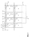
- FIG. 1 shows a circuit schematic diagram for the active matrix drive circuitry of an active matrix type OLED display according to one embodiment of the present invention.
- FIG. 1 shows several rows and columns of pixels. While only a limited number of rows and columns are shown, one skilled in the art can expand this design to a larger plurality of rows and columns.
- OLED display 5 is an RGBX type OLED display having at least four different colored pixels for producing a full color image.
- Each pixel e.g. 20r, 20g, etc.
- Each pixel has an organic light-emitting diode with first and second electrodes, e.g. cathode and anode, and one or more organic light-emitting layers provided between the electrodes.
- Each pixel is addressable, which means the intensity of the pixel can be independently controlled.
- At least three of the different colored pixels are gamut-defining pixels that emit different colors, and which determine the color gamut of the display.
- gamut-defining pixel 20r is arranged to produce red light
- gamut-defining pixel 20g is arranged to produce green light
- gamut-defining pixel 20b is arranged to produce blue light.
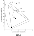
- FIG 9 shows a CIE 1931 xy chromaticity diagram with spectrum locus 900, red emitter 901, green emitter 902, and blue emitter 903.
- the red, green, and blue emitters which are the gamut-defining pixels described herein, define color gamut 905.
- OLED display 5 also has at least one additional pixel, such as pixel 20w, called a within-gamut pixel, which is arranged to emit a within-gamut color light, for example white emitter 904 in FIG 9 .
- Within-gamut pixel 20w most commonly produces white light, in which case the display is an RGBW display.
- the term white is used in the' present invention to indicate any light emission that is perceived as approximately white to a viewer.
- the present invention is not limited to a white pixel and other colors which are, for example, more blue, green, red, yellow, magenta, or cyan in appearance can be also be employed.
- RGBY red, green, blue, yellow
- Such displays can be designated as RGBX displays, wherein X refers to a within-gamut pixel.
- RGBW displays can also refer to the more general RGBX displays.
- OLED display 5 uses within-gamut pixels to reduce power consumption compared to conventional RGB type displays. These within-gamut pixels are more efficient than at least one of the gamut-defining pixels and are typically more efficient than all of the gamut-defining pixels. Efficiency, which can be measured in (cd/A), is determined as the amount of light emitted from the device (the luminance) per unit of current. Power consumed by the device, which can be measured in, for example, watts (W), is determined by the current flow required to produce the desired luminance multiplied by the applied voltage drop (V) across the organic light-emitting diode as well as any circuit components electrically connected between the organic light-emitting diode and the voltage source.
- Efficiency which can be measured in (cd/A)
- Power consumed by the device which can be measured in, for example, watts (W) is determined by the current flow required to produce the desired luminance multiplied by the applied voltage drop (V) across the organic light-emitting diode as well as any circuit components electrical
- within-gamut colors can also be displayed by illuminating the within-gamut pixel in combination with one or more of the gamut-defining pixels at varying intensities. In this way, the RGBW OLED display can produce a full color image at reduced power.
- OLED display 5 has a selected display white point, which is typically specified in CIE 1931 xy chromaticity coordinates. This can have the same chromaticity coordinates as the within-gamut pixel 20w when the within-gamut pixel is a white-emitting pixel. In many cases, the chromaticity coordinates of the within-gamut pixel 20w do not match the chromaticity coordinates of the selected display white point. In these cases, the selected display white point can be provided by activating the within-gamut pixel 20w and one or more of the gamut-defining pixels. Because the display white point is within the color gamut of the gamut-defining pixels, it can also be provided by activating some combination of the gamut-defining pixels alone. It is well known in the art to compute the fractions of each gamut-defining pixel required to match the chromaticity coordinates of the display white point.
- OLED display 5 has a selected display peak luminance, expressed in units such as candelas per square meter or simply as a normalized value such as 100%, which is the maximum luminance of the display at the chromaticity coordinates of the selected display white point.
- the fractions of each gamut-defining pixel required to match the chromaticity coordinates of the display white point may be scaled by the display peak luminance, resulting in a theoretical peak luminance value for each gamut-defining pixel.
- These theoretical peak luminance values are determined as if no within-gamut pixels are used in the display.
- Each gamut-defining pixel has a theoretical peak current to provide the theoretical peak luminance, and a theoretical peak current density based upon the size of each pixel.
- each pixel a nominal peak luminance, a nominal peak current, and a nominal peak current density, each of which can be at or near the theoretical peak values.
- the nominal peak luminance values of each of the within-gamut pixels must be realized in order to provide the display white point at the display peak luminance.
- the display white point and display peak luminance can be provided in the same way, or alternatively, by activating within-gamut pixel 20w alone or with some combination of one or more of the gamut-defining pixels.
- the nominal peak luminance of the within-gamut pixel is the luminance required in this situation to reproduce the display white point at the display peak luminance.
- the nominal peak luminance of a given pixel, gamut-defining or within-gamut, as described herein, can be referred to as one unit of intensity of that pixel.
- Intensity by this definition, is a fraction of the nominal peak luminance, and mixtures of the display pixels can be described as combinations of intensity values.
- an RGB display produces its display white point at its display peak luminance with an intensity triad of (1,1,1).
- an RGBW display whose within-gamut pixel shares the chromaticity coordinates of its display white point can produce the display white point at the display peak luminance with intensity quads of (1,1,1,0), (0,0,0,1), or many other combinations including but not limited to (0.5, 0.5, 0.5, 0.5) or (0.25, 0.25, 0.25, 0.75).
- Luminance correlates with current through the OLED devices in an approximately linear fashion.
- luminance is related to current, which for a given pixel area is related to current density.
- nominal peak luminance is related to nominal peak current, which for a given pixel area is related to nominal peak current density.
- the peak luminance of at least one of the gamut-defining pixels is reduced relative to the corresponding nominal peak luminance. This results in a peak current lower than the nominal peak current for the gamut-defining pixel.
- a lower peak current results in improved power efficiency of the pixel, and, in some cases, improved lifetime for the pixel.
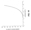
- the peak current densities determine the amount of voltage that must be provided between the first and second electrodes in the OLED device.
- the required OLED voltage for the pixel can be determined from a plot of current density vs. voltage for a given OLED.
- FIG. 10 is an example of such a plot.
- the voltage must be at least 5.5 volts.
- the peak current densities of the gamut-defining pixels are reduced, often resulting in a lower voltage requirement for the pixel.
- a lower voltage requirement results in a further improvement in the power efficiency of the pixel.
- the aforementioned improvements may be gained with each gamut-defining pixel independently, but it is preferable to gain improvements from all three gamut-defining pixels together.
- the active matrix drive circuitry of OLED display 5 comprises signal lines such as select line 113, capacitor line 114, data line 112r, data line 112g, data line 112b, data line 112w, power line 111r, power line 111g, power line 111b, and power line 111w. These signal lines are common to a row or a column of pixels as shown and are arranged to drive the pixels of the row or column.
- the active matrix drive circuitry further includes components such as one or more select transistors, power transistors, and storage capacitors for each pixel, e.g. select transistor 120r; power transistor 140r, and storage capacitor 130r, which together with one of more of the signal lines are arranged to drive the organic light-emitting diode 10r of pixel 20r.
- the other pixels are provided with similar components to drive the respective organic light-emitting diodes of the pixels.
- the drive circuitry regulates luminance of the organic light-emitting diodes of each of the colored pixels by regulating current between zero and the peak current of the pixel.
- the peak current which is the maximum current that the drive circuitry will allow to pass through a given pixel, can be as high as the nominal peak current. For the purposes of this invention, however, the peak current of one or more gamut-defining pixels will be less than its corresponding nominal peak current. This will be described further below.
- the power transistor regulates current through the organic light-emitting diode of the colored pixel, e.g. power transistor 140r regulates current through organic light-emitting diode 10r of pixel 20r.
- a power line is associated with the power transistor of each different colored pixel, e.g. power line 111r is associated with power transistor 140r of red-emitting pixel 20r.
- the power lines associated with the power transistors of each of the different colored pixels e.g. power lines 111r, 111g, 111b, and 111w, are connected together and are connected to a first voltage source 70, designated as VI.
- the term electrical connection is used in this disclosure to indicate connection either directly by way of a conductor or indirectly through a component such as a switch, transistor, diode or the like.
- a common top electrode connection is connected to the cathodes of all the organic light-emitting diodes to complete the circuit.
- This common top electrode connection is electrically connected to a second voltage source 80, designated as Vc.
- Vc second voltage source 80
- the present invention is not limited to the case where the top electrode is common.
- the top electrode can alternately be common to a single column of pixels and each column of pixels can be provided with a different top electrode.
- Other alternate configurations where individual top electrodes are provided for different rows or other groups of pixels or where each pixel is provided with its own isolated top electrode can also be practiced.
- the power line (e.g. 111r) provides current from first voltage source 70 through the power transistor (e.g. 140r) and into the organic light-emitting diode (e.g. 10r) to second voltage source 80. While the circuit of this example is shown with the organic light-emitting diode arranged in a particular bias with the cathode connected to the common connection and the anode connected to the power transistor, the opposite arrangement can also be employed by one skilled in the art and is included within the scope of the present invention.
- the drive circuitry operates in a manner well known in the art.
- Each row of pixels is selected in turn by applying a voltage signal to the select line associated with the row, such as select line 113, which turns on the select transistor, such as select transistor 120r, for each pixel.
- the luminance level, or intensity information, for each pixel is controlled by a voltage signal, which has been set on the data lines, such as data line 112r.
- the storage capacitor, such as storage capacitor 130r, for each pixel is then charged to the voltage level of the data line associated with that pixel and maintains the data voltage until the row is selected again during the next image frame.
- the storage capacitor 130r is connected to the gate terminal of the power transistor 140r.
- Power transistor 140r regulates the current flow through its source and drain terminals and to the organic light-emitting diode 10r in response to the voltage level held on its gate terminal by storage capacitor 130r, thereby regulating the pixel's luminance.
- Each row is then unselected by applying a voltage signal to the select line, which turns off the select transistors.
- the data line signal values are then set to the levels desired for the next row and the select line of the next row is turned on. This is repeated for every row of pixels.
- select lines are signal lines that serve the function of isolating a row of pixels so that the intensity information can be loaded into the pixels of the row.
- Data lines are signal lines that provide the intensity information to the pixels, that is, a signal corresponding to the luminance of a given pixel. This intensity information can be in the form of a voltage or current signal.
- Power lines are signal lines that provide a source of electrical power to the organic light-emitting diodes of the pixels for maintaining the luminance level of the pixel, at least during the time when the pixels row is not selected by the select line. Typically, the power lines provide a source of electrical power to the organic light-emitting diode at all times when the pixels are illuminated.
- the voltage differential, V1-Vc, is the required display voltage. This voltage is typically determined by summing the required OLED voltage for the display (Voled), a voltage allowance for OLED aging (Vaging), the required TFT voltage (Vds), and a voltage allowance for resistive losses in the supply lines (Vres).
- the required OLED voltage for the display, Voled is the maximum of the OLED voltages required for each pixels.
- the required OLED voltage for each of the gamut-defining pixels is reduced because the peak current in each pixel is reduced. As long as the required OLED voltage for the gamut-defining pixels was originally higher than the required OLED voltage for the within-gamut pixel, which is often the case, the required OLED voltage for the display will be reduced.
- the lower peak currents in each of the pixels result in lower peak current flows through the power lines (e.g. 111r) and through the power transistors (e.g. 140r). If the power lines remain the same size, a lower peak display current results in a lower resistive voltage drop allowance, Vres. Therefore, the required display voltage (V1-Vc) can be reduced even further. Any reduction in the required display voltage results in an improvement in power efficiency for the display. Alternately, the backplane designer may choose to keep the voltage drop the same by reducing the size of the power lines. This reduction of the power line size can be traded off for other display performance improvements, such as increased display lifetime or higher resolution by one skilled in the art.
- the magnitude of the maximum voltage applied by the drive circuitry to the pixels which is the magnitude of V1-Vc, is selected to be less than the magnitude of the voltage needed to fully drive the gamut-defining pixels, in this case pixel 20r, pixel 20g, and pixel 20b, but equal to or greater than the voltage needed to fully drive the within-gamut pixel, in this case pixel 20w.
- the maximum voltage is applied across first and second electrodes of the different colored pixels; these electrodes will be described further below. Selecting the maximum voltage as described herein is possible because the luminance of the organic light-emitting diode of each of the colored pixels is regulated such that the sum of the gamut-defining pixel peak luminances will be less than the display peak luminance. In other words, the maximum intensity for one or more of the gamut-defining pixels will be somewhat less than unity. While this is not always desirable in a display, in circumstances where low power consumption and/or longer device lifetime are paramount considerations, it can be an acceptable trade-off.
- a plurality of pixels having the same color can be present in a plurality of rows and columns.
- a given column of pixels can include all red pixels and the entire column is therefore preferably connected to the same power line, as shown.
- every fourth column of pixels can include all pixels of the same color. It is preferred that all the pixels be connected the same voltage level.
- the connecting of power lines of differing columns can be achieved by electrically connecting these power lines together with a conductor on one side of the display outside the pixel area.
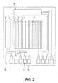
- FIG. 2 shows a conceptual view of a display illustrating the layout and wiring of the various parts and sections of a display according one embodiment of the present invention.
- the display includes a pixel region 30, a connector region 40, a select line driver 50, and a data line driver 60.
- the select line driver 50 functions to selectively activate the select lines (not shown) for each row as previously described.
- the data line driver 60 serves to provide data signals to the data lines (not shown) for each column as previously described.
- the pixel region 30 includes the light-emittirig pixels of the display. The regions outside of the pixel region 30 are non-light-emitting regions.
- the connector region 40 provides a plurality connector pads such connector pad 41 and connector pad 42.
- connector pads serve as a location for bonding of wires or cables that electrically connect the display to external power sources (not shown) or controlling circuits (not shown).
- connector pad 41 serves as a connection for the second voltage source Vc
- connector pad 42 serves as a connection for the first voltage source V1. It is preferable that the connector pads are all formed along one edge of the display and that the power lines associated with the power transistors of the different colored pixels, described above, are connected together on one side of the display, e.g.
- connector pad 42 is electrically connected to power lines such as power line 111r, power line 111g, power line 111b, and power line 111w outside of the pixel region 30, to reduce the size of the non-light-emitting regions of the display as well as simplify the connection process. While each of the voltages sources can be electrically connected to a single connector pad, multiple connector pads can also be used to provide a low resistance electrical connection to one or more of the voltage sources as described in U.S. Patent 6,531,815 .
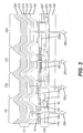
- FIG. 3 A cross-sectional view illustrating the vertical arrangement of the various layers of an OLED display is shown in FIG. 3 . From FIG. 3 , it can be seen that pixel 20r, pixel 20g, pixel 20b, and pixel 20w are formed above substrate 100. When electrically stimulated, these pixels produce light emission 280r, 280g, 280b and 280w respectively. Active matrix circuitry layers 200, including insulating layer 202, insulating layer 204, and insulating layer 207 are shown. The formation of the interpixel dielectric layer 160 over the edges of the first electrodes, such as first electrode 181, can also be seen.
- these first electrodes are preferably constructed of a material that is highly transparent such as indium tin oxide.
- the present invention is not limited to this configuration, and devices can be constructed which emit in the opposite direction.
- the first electrodes are preferably constructed of a material that is reflective, such as aluminum or silver.
- Each of the pixels further includes a portion of organic EL media 210.
- organic EL media 210 there are numerous configurations of the organic EL media 210 layers wherein the present invention can be successfully practiced.
- a broadband or white light source that emits light at the wavelengths used by all the pixels can be used to avoid the need for patterning the organic EL media between pixels.
- color filter elements such as color filter element 230r, color filter element 230g, and color filter element 230b, are provided for the gamut-defining pixels in the path of the light to produce the desired light colors from the white or broadband emission for a multi-color display. Pixels that are to emit the same white or broadband emission as the organic EL media, such as pixel 20w, can remain unfiltered.
- a transparent filler 230w can optionally be provided in place of a color filter element.
- organic EL media layers that emit broadband or white light are described, for example, in U.S. Patent 6,696,177 .
- the present invention can also be made to work where each pixel has one or more of the organic EL media layers separately patterned for each pixel to emit differing colors for specific pixels.
- the organic EL media 210 is constructed of several layers such as; a hole-injecting layer 211, a hole-transporting layer 212 that is disposed over hole-injecting layer 211, an organic light-emitting layer 213 disposed over hole-transporting layer 212, and an electron-transporting layer 214 disposed over light-emitting layer 213.
- Organic EL media layers applied in the opposite order are also known in the art and can be applied to the present invention.
- These organic EL media layers include organic materials that are either small molecule materials or polymer materials as is known in the art.
- These organic EL media layers can be deposited by one or more of several methods known in the art such as, for example, thermal evaporation in a vacuum chamber, laser transfer from a donor substrate, or deposition from a solvent by spin coating or use of an ink jet print apparatus.
- a second electrode 220 is formed above the organic EL media 210.
- this electrode is preferably highly reflective and can be composed of a metal such as aluminum, silver, or magnesium/silver alloy. However, in an alternate embodiment where the light is viewed in the opposite direction, this electrode should be highly transparent and constructed of thin metals, such as silver with a thickness less than 25 nm, or transparent conductive oxides such as indium tin oxide, or combinations thereof.
- the second electrode 220 can also include an electron injecting layer (not shown) composed of a material such as lithium to aid in the injection of electrons.
- OLED displays are sensitive to moisture or oxygen, or both, so they are commonly sealed with an encapsulating structure (not shown) in an inert atmosphere such as nitrogen or argon using metal or glass covers, along with a desiccant such as alumina, bauxite, calcium sulfate, clays, silica gel, zeolites, alkaline metal oxides, alkaline earth metal oxides, sulfates, or metal halides and perchlorates.
- Methods for encapsulation and desiccation include, but are not limited to, those described in U.S. Patent 6,226,890 .
- barrier layers such as SiOx, Teflon, and alternating inorganic/polymeric layers are known in the art for encapsulation and can be applied to the present invention by one skilled in the art.
- the color filter elements shown in FIG. 3 are disposed in the path of the light produced in the emitting areas of the gamut-defining pixels so as to filter the color of the light prior to reaching the observer.
- the within-gamut pixel can optionally be provided with a transparent filler material or a color filter element to slightly modify its color. Alternately, the present invention can also be successfully practiced without providing a transparent filler material or color filter element for the within-gamut pixel.
- FIG. 1 shows the pixels arranged in a stripe pattern, wherein pixels of the same color are aligned in the same column or row.
- the present invention is not limited to this case and alternate patterns where different colored pixels are arranged in the same columns or same rows can also be applied to the present invention.
- One pixel arrangement pattern that is particularly useful is a quad pattern where the four different colored pixels are arranged in a rectangular fashion involving two rows and two columns. Quad patterns are advantageous in that the all four different colored pixels are close to each other, thereby reducing the perception of band defects when one or more of the pixels are not illuminated in an image or portion of an image.
- Gamut-defining pixel 20r, gamut-defining pixel 20g, gamut-defining pixel 20b, and within-gamut pixel 20w can be constructed to emit red (R) light, green (G) light, blue (B) light, and white (W) light, respectively.
- R red
- G green
- B blue
- W white
- the present invention is not limited to these specific colors and other colors can also be applied to the present invention by one skilled in the art.
- power line 111 is provided, which is electrically connected to each pixel. Specifically, a power transistor such as 140w is electrically connected to power line 111 by way of a via as shown. Power line 111 is electrically connected to a voltage source (not shown) that controls the magnitude of the voltage applied to the within-gamut pixel and the gamut-defining pixels. Since this arrangement provides only a single power line 111 for the four different colored pixels compared to the four shown for the stripe pattern of some of the other embodiments, the space occupied on the substrate by the power lines is reduced.
- FIG. 4 further shows the construction and layout of the various circuit components such as select transistor 120r, storage capacitor 130r, and power transistor 140r.
- the drive circuitry components are fabricated using known integrated circuit and thin film transistor fabrication technologies.
- Select transistor 120r is formed from a first semiconductor region 121 using techniques well known in the art.
- Select transistor 120r is shown as a double gate type transistor, however, this is not required for successful practice of the present invention and a single gate type transistor can also be used.
- power transistor 140r is formed in a second semiconductor region 141.
- the first semiconductor region 121 and second semiconductor region 141 are preferably formed from the same semiconductor layer.
- This semiconductor layer is preferably silicon such as polycrystalline or crystalline silicon, but can also be amorphous silicon.
- This first semiconductor region 121 also forms one side of storage capacitor 130r.
- an insulating layer (not shown) of a material such as silicon nitride that forms the gate insulator of select transistor 120r, the gate insulator for power transistor 140r, and the insulating layer of storage capacitor 130r.
- the gate of select transistor 120r is formed from part of select line 113, which is formed in the first conductor layer.
- Power transistor 140r has a separate power transistor gate 143 also preferably formed in the first conductor layer.
- the other electrode of storage capacitor 130r is formed as part of capacitor line 114, which is also preferably formed from the first conductive layer.
- Power line 111, data line 112r, data line 112g, data line 112b, and data line 112w are preferably formed from a second conductive layer.
- these signal lines are preferably fabricated from multiple conductive layers with at least one interlayer insulating layer (not shown) of a material such as silicon nitride disposed in between.
- the first electrode 181 of the organic light-emitting diode is connected to power transistor 140r.
- An insulating layer (not shown) of a material such as silicon nitride is located between the first electrode 181 and the second conductive layer.
- Connections between layers are formed by etching holes (or vias) in the insulating layers.
- Via 142 connects the power transistor gate 143 to first semiconductor region 121
- via 149 connects second semiconductor region 141 to power line 111
- via 145 connects second semiconductor region 141 to the first electrode 181.
- data line 112b should be crossed. This is achieved using conductive bridge 124, which electrically connects to data line 112r by way of via 125 and to select transistor 120r by way of via 127.
- Conductive bridge 124 is constructed in a different conductor layer than the data lines, preferably the same conductor layer as the select lines.
- First electrode 181 serves to provide electrical contact to the organic electroluminescent media of the organic light-emitting diodes.
- an interpixel dielectric layer can be formed to cover the edges of the electrodes and reduce shorting defects as described below. Such interpixel dielectric layers are also described in U.S. Patent 6,246,179 .
- Opening 182 is made in the interpixel dielectric layer over the first electrode 181 to permit the first electrode 181 to make electrical contact with the organic electroluminescent media of the organic light-emitting diode.
- the emitting area of pixel 20r is defined by the areas of the first electrode 181 that is in electrical contact with the organic electroluminescent media.
- the emitting area is the area of the first electrode 181 reduced by any area covered by dielectric material. Therefore, when an interpixel is used as described, the emitting area is the area of the opening, such as opening 182, in the interpixel dielectric layer. While use of such an interpixel dielectric layer is preferred, it is not required for successful practice of the present invention.
- FIG. 5 a block diagram of a method for operating an OLED display for producing a full color image at reduced power in accordance with this invention.
- a plurality of at least four different colored pixels is provided, including three different colored addressable gamut-defining pixels and a fourth addressable within-gamut pixel (Step 310), for example, by constructing an OLED display as described herein.
- Each pixel has an organic light-emitting diode with first and second electrodes and one or more organic light-emitting layers provided between the electrodes.
- drive circuitry as described above is provided for applying a maximum voltage and for regulating the current-and thus the luminance-of each pixel.
- a display white point is selected (Step 320). The exact display white point selected will depend on a number of factors, for example, the properties of the display and the expected usage conditions.
- a display peak luminance is selected (Step 330). The display peak luminance is the maximum luminance that the display can produce, and can be selected by the choices of construction of the display.
- Gamut-defining pixel peak luminances are selected (Step 340), and a within-gamut pixel peak luminance is selected (Step 350), which can be selected by choices of construction of the display and the pixels, and by the maximum current which will be used in the pixels. The order of Steps 320 to 350 can vary.
- the luminance of the organic light-emitting diode of each of the colored pixels is regulated (Step 360) such that the sum of the gamut-defining pixel peak luminances is less than the display peak luminance. Further details of the luminance regulation step will be described.
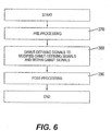
- FIG. 6 is a block diagram showing the luminance regulation step (Step 360) of FIG. 5 in greater detail.
- Luminance regulation can include converting gamut-defining pixel signals to modified gamut-defining pixel signals and within-gamut pixel signals (Step 380).
- Such a conversion step has been taught by Murdoch et al. in US 6,897,876 B2 , the contents of which are incorporated by reference.
- a method is described for transforming three color input signals (R, G, B), corresponding to three gamut-defining color primaries, to four color output signals (R', G', B', W) corresponding to the three gamut-defining pixels and a fourth within-gamut pixel.
- Luminance regulation can also include one or more pre-processing steps (Step 370) and one or more post-processing steps (Step 390).
- pre-processing steps are those operations to be described below that are performed on one or more of the three color input signals (R, G, B).
- Post-processing steps are those to be described below that are performed on one or more of the four color output signals (R', G', B', W).
- post-processing steps will primarily be performed on the R', G', and B' signals. Pre-processing and post-processing steps will be described in more detail.
- the within-gamut pixel is more efficient than at least one of the gamut-defining pixels and is typically more efficient than all of the gamut-defining pixels. This means that the current-and therefore also the power-needed to drive the within-gamut pixel to maximum luminance is less than that needed for the less efficient gamut-defining pixels.
- the sum of the gamut-defining pixel peak luminances would be less than the display peak luminance.
- the gamut-defining pixel peak luminances would not be able to achieve unit intensity in the infrequent occasions where unit intensity of only one or two colors is required.
- this can have an unpleasant effect on the display, e.g. loss of texture or hue shifts.
- it is necessary in this case to also include a method of regulating the luminance of the gamut-defining pixels to minimize unpleasant color effects while also saving power.
- the operations described below will provide luminance regulation by mapping a range of input signals, each corresponding to a gamut-defining pixel luminance, into a narrower range of gamut-defining pixel luminances.
- the Y values have units of luminance, such as cd/m 2 .
- white point luminance is often normalized to a dimensionless quantity with a value of 100, making it effectively percent luminance factor.
- luminance will always be used to refer to percent luminance factor, and XYZ tristimulus values will be used in the same sense.
- a common display white point of D65 with xy chromaticity values of (0.3127, 0.3290) has XYZ tristimulus values of (95.0, 100.0, 108.9).
- the nominal peak luminance of the R, G, and B pixels are selected such that when all three emit light at nominal peak luminance, wherein each receives its nominal peak current, they produce the display white point and peak luminance, for example a luminance of 200 cd/m 2 at the D65 point.
- the RGB pixels will never all be on together, since the W will be used in their stead to produce some or all of the luminance.
- accurate color reproduction of all colors in the additive RGB gamut requires that the RGB pixels be able to reach their nominal peak luminance.
- pmat a phosphor, or primary matrix (pmat).
- ITU-R Rec. BT.709 (HDTV) primaries and white point (D65), and working in percent luminance factor, the pmat is: pma t RGB 41.2 35.8 18.0 21.3 71.5 7.2 1.9 11.9 95.1
- the first column contains the XYZ tristimulus values of the R pixel at nominal peak luminance, the second the G pixel, and the third the B pixel. Looking at the middle row of the pmat, this means that the R pixel at nominal peak luminance has a luminance Y of 21.3, while the G and B have luminances of 71.5 and 7.2, respectively. Because the luminances are actually percent luminance factors, meaning they have been normalized to 100% of the display peak luminance, these three percent luminance factors sum to 100, and the R contributes 21.3% of the luminance to make white.
- RGBW system adds a fourth column to the pmat, the XYZ tristimulus values of the W pixel.
- the W primary has the same chromaticity coordinates as the display white point, meaning it can be used alone to produce white. This simple case is convenient because it obviates the normalization steps that the RGB-to-RGBW algorithm employs.
- the W pixel intensity is normalized such that the RGB pixels can reproduce its color, and this unit intensity can be used as the W nominal peak luminance.
- the RGB peak luminances sum to 100% of the display peak luminance.
- there are a number of ways to reduce the red peak luminance signal e.g. clipping, scaling, nonlinear compression, desaturation, and dimming. Each variation is described below.
- RGB-to-RGBW conversion is made with 100% white mixing ratio (WMR), which is the portion of the common luminance that is transferred from the RGB pixels to the W pixel.
- WMR white mixing ratio
- the method may be applied for other values of WMR, such as 50% or 75%, typically with some increase in power requirement.
- a common limit value will be used for all three gamut-defining pixels, but the method does not preclude different limits for each pixel.
- initial input signals will be represented as RGB, while those resulting from the RGB-to-RGBW conversion described by Murdoch et al. will be represented as R'G'B'W.
- Further signals resulting from post-processing Step 390 of FIG. 6 will be represented as R"G"B"W. Since W is often unchanged in many of these operations, it will not always be shown in all examples.
- signals from pre-processing step 370 will be represented as R ⁇ G ⁇ B ⁇ .
- RGBW values are modified in various ways. It is important to remember that the relative ratios between the RGBW values determine the chromaticity coordinates of the color that will be produced by the display. Thus, RGBW quads (1,0.5,0,0) and (0.5,0.25,0,0), both having the R:G:B:W ratio 2:1:0:0, have the same chromaticity coordinates, even though the overall luminance of the first is twice that of the second. Algorithms that preserve R:G:B:W signal ratios generally do not distort chromaticity coordinates, and the term "preserving color accuracy" is used to describe this behavior. Ignoring the W signal is appropriate if the W pixel and the display white point have the same or similar chromaticity coordinates.
- the R:G:B ratio describes the "hue" of the color, which can remain constant even if the W changes, and likewise the chromaticity coordinates change.
- Algorithms can preserve the R:G:B signal ratio, and the term “preserving hue” is used to describe this behavior.
- the term "saturation” is used in the colloquial fashion to describe the purity of a color, which is also described by the relationship between the RGBW values.
- a color of high saturation has a low W value and large ratio between the maximum and minimum RGB values, eg the RGBW quad (1,0,0.1,0) represents a highly saturated color because W is 0 and the ratio between the max RGB (1) and the min RGB (0) is large.
- the RGBW quad (1,1,0.9,0) is unsaturated because, while the W is 0, the ratio between the max (i) and the min (0.9) is close to unity.
- Algorithms that lower the purity of colors are referred to as desaturating, which means a full or partial suppression of the color information without disturbance of the luminance information in an image.
- the general case allows for the limits to differ in the R', G', and B' pixels, but it is likely that they will all be the same. For example, if the limit is 0.75 for R'G'B', then any values below 0.75 remain untouched, while all values above that limit are crushed to 0.75. This unprejudiced crushing may eliminate variation, and thus texture, in colored regions of an image. Considering the endpoints, a limit of 1 results in an unmodified image, while a limit of 0 results in the W image. Because the W image intensity correlates directly with luminance and inversely with saturation with respect to the input image, the resulting image is generally rather unpleasant.
- clipping is a nonlinear operation, it can also upset the R:G:B signal ratio, which can result in changed chromaticity coordinates. For example, inputting a yellow color wherein the red signal is more intense than that of green, the red will get clipped first and thus the yellow can display a shift toward green.
- the R'G'B'W signal is scaled by [0.75 0.75 0.75 1.0].
- the result is a loss of luminance in the colored regions of an image, with no effect on neutrals, colors having chromaticity coordinates the same or similar to the display white point.
- Scaling differs from clipping in that texture is compressed rather than destroyed, but the tradeoff is a loss of luminance in all colored regions, , rather than just those that exceed the limit. Because the scaling is applied to all non-neutral colors, it appears that quality is lost relatively quickly as the limit is lowered from 1.
- One benefit of scaling is that it preserves hue. Because the RGB signals are scaled together, the R:G:B signal ratios are unchanged.
- Nonlinear compression can also be called soft clipping.
- a combination of the scaling and clipping approaches, nonlinear compression scales a portion of the R'G'B' intensity range and leaves the rest untouched. For example, for a limit of 0.75, a nonlinear compression might involve leaving the (0, 0.6) interval untouched, and then squeezing the (0.6, 1) interval into the limited (0.6, 0.75) range.
- this can be done using a smooth function rather than piecewise linear, and the bend-over threshold (R' thresh , 0.6 in this example) can be adjusted higher or lower.
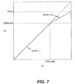
- FIG. 7 is a graph showing one embodiment of luminance regulation by non-linear mapping in accordance with this invention. Specifically, FIG. 7 shows the above piecewise linear function, which could easily be interpreted as a LUT from R' to R" for mapping a range of input signals into a narrower range of gamut-defining pixel luminances. Below the bend-over threshold R' thresh , the slope is unity and the input value is unchanged. Above the threshold, the slope m is less than one. Images processed with nonlinear compression appear like a combination of clipping and scaling. Some texture detail is retained, in contrast to clipping, but it is less visible than with scaling. Likewise, the luminance of objects are somewhere between those in the preceding examples. This nonlinear approach has the same hue-changing side effect as clipping, because each signal can be modified independently, changing the R:G:B signal ratios.
- the nonlinear algorithm compresses R' by a factor between 1 and the R'G'B' limit, depending on its intensity. Since G' is lower to begin with, it is compressed by a smaller factor, meaning that the resultant R:G ratio is lower than it was at the start.
- the nonlinear compression algorithm can be improved by including a hue-preserving step, which follows the above algorithm with a restoration of the red, green, and blue ratios. This is done by lowering the remaining signals by the same scale factor that was applied to the highest intensity signal.
- a single scale factor may be computed for the largest of the three gamut-defining pixel signals, and that factor applied to all three signals.
- G' is compressed further than with nonlinear compression, such that the R:G ratio is restored.
- all three gamut-defining pixel intensity values are scaled by the factor determined by nonlinear compression of the highest value.
- the hue preservation step results in lower power relative to the unmodified nonlinear compression solution.
- a variation on the above algorithms can be made by limiting the luminance of the secondary colors, rather than the primary colors.
- the gamut-defining primaries are RGB
- the secondaries are the pairwise combinations of them, R+G (yellow, Y), R+B (magenta, M), and G+B (cyan, C).
- An embodiment of the current invention includes regulating the sum of peak currents-and peak luminances-for any two gamut-defining pixels, such that the sum is less than the sum of the nominal peak currents-and peak luminances-of the corresponding pixels. This process can be done instead of, or in addition to, regulating the peak luminance of RGB. This concept can be applied to any of the algorithms described herein with little modification.
- the CMY values are computed, for example using a simple matrix operation, which includes a normalization factor of 1/2 to keep the CMY values within the range of 0 to 100%:
- C M Y 1 2 0 1 1 1 0 1 1 1 0 ⁇ R ′ G ′ B ′
- the CMY values are provided to a LUT or piecewise function, resulting in three scale factors, and the minimum scale factor is selected and applied to the R'G'B' values, again leaving W unchanged.
- the CMY limit can be used wherever the RGB limit is discussed, either alone or in combination with an RGB limit.
- the CMY limit has a smaller impact than the RGB limit for a given limit value, because the primaries are affected half as severely as the secondaries. For this reason, the CMY limit is less effective than the RGB limit at reducing the RGB peak luminances, but very effective at reducing sums of the peak luminances. Because an RGBW display employing 100% WMR will result in one of the gamut-defining pixels emitting no light for an arbitrary color being reproduced on the display, the CMY limit is a good way to limit the total luminance of the other two gamut-defining pixels, which results in limiting the total current required by said pixels.
- the dsmat is a linear combination of an identity matrix and a luminance matrix.
- the rows in the luminance matrix are replicates of the second row of the sRGB pmat, which are the nominal peak luminances of the R, G, and B pixels.
- an RGB signal multiplied by the luminance matrix will result in three identical luminance values, each equal to the sum of the luminance contribution of the three pixels.
- the luminance matrix since it is expressed in percent luminance factor, is divided by 100. With high values of v , the identity matrix dominates, meaning the dsmat has little or no effect on the RGB image. With low values, the luminance matrix dominates. Intermediate values blend the two endpoints smoothly.
- the luminance of the image is preserved, while the saturation is smoothly reduced; i.e., the image approaches a luminance-only image.
- a result identical to desaturation can be reached by following an R'G'B' scaling operation with a luminance adjustment to the W signal. Since desaturation is easier to implement, it is preferred.
- the desaturation algorithm differs from those preceding because it modifies the W pixel intensity.
- the preceding algorithms all reduce RGB values and leave W unchanged, which will always result in less power being used in an AMOLED display. Desaturation, however, because it increases the W to compensate for the RGB reduction, will result in lower power if the efficiency of the W pixel is sufficiently greater than the efficiency of the RGB pixels.
- the combined algorithm has two main degrees of freedom: the amount of desaturation as determined above by the parameter v, and the RGB limit applied in the nonlinear compression.
- Additional variables can include a bend-over threshold in the nonlinear compression, or more generally the nonlinear shape of the intensity limiting LUT.
- a parameterized LUT is used that depends only on the RGB limit, thus leaving the original two degrees of freedom.
- the LUT is defined as a piecewise function with a smooth slope transition to avoid the abrupt transition presented at R' thresh in FIG. 7 .
- FIG. 8 which shows another embodiment of luminance regulation by non-linear mapping in accordance with this invention, shows this smooth slope transition.
- the LUT has a unity slope below the transition region, and a slope of m above the transition region, thereby compressing the input values in the domain in or above the transition region.
- the smooth curve in the gray transition region is, for example, a cubic function that matches the slopes of the unity- and m -sloped regions at its endpoints.
- R' thresh is computed as 0.75 times R' lim
- the transition region is R' thresh ⁇ 0.1, but these values can be modified according to need.
- m is the slope of the upper region as defined above
- w is the half-width of the transition region
- the cubic polynomial coefficients a , b , c , and d are selected such that the cubic function's values and derivatives match the linear functions at the endpoints of the transition region. Given the endpoint constraints for a given system, one can solve for a , b , c , and d with known methods.
- a selected RGB limit can be used in the computation of LUTs using the preceding steps, and an independently selected desaturation parameter v can be used in computing desaturation matrices as described above.
- the exact parameters chosen will depend upon a number of factors, including the properties of the gamut and within-gamut pixels, types of images foreseen to be displayed on the device, and usage conditions, e.g. ambient lighting.
- the combination algorithm first applies the desaturation matrix to the RGB data, then performs the R ⁇ G ⁇ B ⁇ -to-R'G'B'W conversion, then applies the nonlinear compression, preserving hue.
- the W pixel described here is slightly red-orange in color, compared to the neutral display white point. Starting from a pleasing color reproduction using RGBW, if the RGB values are lowered and the W left alone, the red-orange of the W will begin to dominate. To correct this, some amount of red-orange, in this case a bunch of red and a little green, must be removed from the image by tweaking the RGB values.
- the RGB values may be corrected "upward," which poses the risk that they may run into a limit and be clipped.
Landscapes
- Engineering & Computer Science (AREA)
- Physics & Mathematics (AREA)
- Computer Hardware Design (AREA)
- General Physics & Mathematics (AREA)
- Theoretical Computer Science (AREA)
- Electroluminescent Light Sources (AREA)
- Control Of El Displays (AREA)
- Control Of Indicators Other Than Cathode Ray Tubes (AREA)
Applications Claiming Priority (2)
| Application Number | Priority Date | Filing Date | Title |
|---|---|---|---|
| US11/312,872 US7586497B2 (en) | 2005-12-20 | 2005-12-20 | OLED display with improved power performance |
| PCT/US2006/046461 WO2007075276A1 (en) | 2005-12-20 | 2006-12-06 | Oled display with improved power performance |
Publications (2)
| Publication Number | Publication Date |
|---|---|
| EP1964091A1 EP1964091A1 (en) | 2008-09-03 |
| EP1964091B1 true EP1964091B1 (en) | 2019-06-26 |
Family
ID=37908296
Family Applications (1)
| Application Number | Title | Priority Date | Filing Date |
|---|---|---|---|
| EP06839049.1A Active EP1964091B1 (en) | 2005-12-20 | 2006-12-06 | Oled display with improved power performance |
Country Status (5)
| Country | Link |
|---|---|
| US (1) | US7586497B2 (enExample) |
| EP (1) | EP1964091B1 (enExample) |
| JP (1) | JP5363116B2 (enExample) |
| TW (1) | TWI380261B (enExample) |
| WO (1) | WO2007075276A1 (enExample) |
Families Citing this family (143)
| Publication number | Priority date | Publication date | Assignee | Title |
|---|---|---|---|---|
| CN101171594A (zh) * | 2005-04-04 | 2008-04-30 | 克雷沃耶提公司 | 实现低成本全范围映射算法的系统和方法 |
| GB2441354B (en) * | 2006-08-31 | 2009-07-29 | Cambridge Display Tech Ltd | Display drive systems |
| US8933972B2 (en) * | 2007-02-01 | 2015-01-13 | Google Technology Holdings LLC | Luminance adjustment in a display unit |
| US20080252797A1 (en) * | 2007-04-13 | 2008-10-16 | Hamer John W | Method for input-signal transformation for rgbw displays with variable w color |
| US20100033456A1 (en) * | 2007-05-14 | 2010-02-11 | Keisuke Yoshida | Display device and display method thereof |
| US9620038B2 (en) * | 2007-08-08 | 2017-04-11 | Landmark Screens, Llc | Method for displaying a single image for diagnostic purpose without interrupting an observer's perception of the display of a sequence of images |
| US9342266B2 (en) * | 2007-08-08 | 2016-05-17 | Landmark Screens, Llc | Apparatus for dynamically circumventing faults in the light emitting diodes (LEDs) of a pixel in a graphical display |
| US9262118B2 (en) * | 2007-08-08 | 2016-02-16 | Landmark Screens, Llc | Graphical display comprising a plurality of modules each controlling a group of pixels corresponding to a portion of the graphical display |
| US9659513B2 (en) | 2007-08-08 | 2017-05-23 | Landmark Screens, Llc | Method for compensating for a chromaticity shift due to ambient light in an electronic signboard |
| US9536463B2 (en) * | 2007-08-08 | 2017-01-03 | Landmark Screens, Llc | Method for fault-healing in a light emitting diode (LED) based display |
| US9779644B2 (en) * | 2007-08-08 | 2017-10-03 | Landmark Screens, Llc | Method for computing drive currents for a plurality of LEDs in a pixel of a signboard to achieve a desired color at a desired luminous intensity |
| FR2923067B1 (fr) * | 2007-10-25 | 2010-05-21 | St Microelectronics Grenoble | Procede de traitement d'un flux video numerique et dispositif correspondant. |
| JP4614106B2 (ja) | 2008-06-18 | 2011-01-19 | ソニー株式会社 | 自発光表示装置および電子機器 |
| US8237642B2 (en) * | 2008-07-14 | 2012-08-07 | Global Oled Technology Llc | Method for improving display lifetime |
| US20100225673A1 (en) | 2009-03-04 | 2010-09-09 | Miller Michael E | Four-channel display power reduction with desaturation |
| US8169389B2 (en) | 2008-07-16 | 2012-05-01 | Global Oled Technology Llc | Converting three-component to four-component image |
| JP5091796B2 (ja) * | 2008-08-05 | 2012-12-05 | 株式会社東芝 | 画像処理装置 |
| US8184112B2 (en) * | 2008-09-24 | 2012-05-22 | Global Oled Technology Llc | Increasing dynamic range of display output |
| BRPI0921663A2 (pt) * | 2008-11-13 | 2016-02-16 | Sharp Kk | dispositivo de diaplay |
| US8102341B2 (en) * | 2008-12-17 | 2012-01-24 | Getac Technology Corporation | Display system and driving method thereof |
| US8619008B2 (en) * | 2009-02-13 | 2013-12-31 | Global Oled Technology Llc | Dividing pixels between chiplets in display device |
| US8466856B2 (en) * | 2011-02-22 | 2013-06-18 | Global Oled Technology Llc | OLED display with reduced power consumption |
| US8912023B2 (en) | 2009-04-08 | 2014-12-16 | Ledengin, Inc. | Method and system for forming LED light emitters |
| US8384097B2 (en) * | 2009-04-08 | 2013-02-26 | Ledengin, Inc. | Package for multiple light emitting diodes |
| US20100301758A1 (en) * | 2009-06-02 | 2010-12-02 | Mitac Technology Corp. | Flat display device blacklight module thereof for night vision imaging system |
| US20110069089A1 (en) * | 2009-09-23 | 2011-03-24 | Microsoft Corporation | Power management for organic light-emitting diode (oled) displays |
| US20110109773A1 (en) * | 2009-11-10 | 2011-05-12 | General Electric Company | System and method for adaptive nonlinear compressed visual sensing |
| KR101225192B1 (ko) * | 2009-11-23 | 2013-01-22 | 에스케이텔레콤 주식회사 | Rgbw 컬러입자를 이용한 컬러전자종이 및 이의 구동방법 |
| JP5577719B2 (ja) * | 2010-01-28 | 2014-08-27 | ソニー株式会社 | 表示装置およびその駆動方法ならびに電子機器 |
| KR101108167B1 (ko) * | 2010-02-12 | 2012-02-06 | 삼성모바일디스플레이주식회사 | 유기 발광 디스플레이 장치 |
| US9161448B2 (en) | 2010-03-29 | 2015-10-13 | Semprius, Inc. | Laser assisted transfer welding process |
| US8858022B2 (en) | 2011-05-05 | 2014-10-14 | Ledengin, Inc. | Spot TIR lens system for small high-power emitter |
| US9345095B2 (en) | 2010-04-08 | 2016-05-17 | Ledengin, Inc. | Tunable multi-LED emitter module |
| US9080729B2 (en) | 2010-04-08 | 2015-07-14 | Ledengin, Inc. | Multiple-LED emitter for A-19 lamps |
| WO2012027458A1 (en) | 2010-08-26 | 2012-03-01 | Semprius, Inc. | Structures and methods for testing printable integrated circuits |
| TWI423221B (zh) | 2010-10-27 | 2014-01-11 | Au Optronics Corp | 主動式矩陣有機發光二極體顯示面板的驅動方法 |
| US9899329B2 (en) | 2010-11-23 | 2018-02-20 | X-Celeprint Limited | Interconnection structures and methods for transfer-printed integrated circuit elements with improved interconnection alignment tolerance |
| US8334859B2 (en) * | 2011-03-28 | 2012-12-18 | Au Optronics Corporation | Electroluminescent display and method of driving same |
| US8934259B2 (en) | 2011-06-08 | 2015-01-13 | Semprius, Inc. | Substrates with transferable chiplets |
| US9412727B2 (en) | 2011-09-20 | 2016-08-09 | Semprius, Inc. | Printing transferable components using microstructured elastomeric surfaces with pressure modulated reversible adhesion |
| JP5884385B2 (ja) * | 2011-10-06 | 2016-03-15 | セイコーエプソン株式会社 | 画像処理装置、表示装置及び画像処理方法 |
| US11032884B2 (en) | 2012-03-02 | 2021-06-08 | Ledengin, Inc. | Method for making tunable multi-led emitter module |
| JP5124051B1 (ja) * | 2012-03-02 | 2013-01-23 | シャープ株式会社 | 表示装置 |
| TWI460712B (zh) * | 2012-08-21 | 2014-11-11 | Au Optronics Corp | 顯示器之色域補償方法 |
| US9666119B2 (en) | 2012-08-30 | 2017-05-30 | Apple Inc. | Systems and methods for controlling current in display devices |
| WO2014054449A1 (ja) * | 2012-10-01 | 2014-04-10 | シャープ株式会社 | 回路基板及び表示装置 |
| US9234801B2 (en) * | 2013-03-15 | 2016-01-12 | Ledengin, Inc. | Manufacturing method for LED emitter with high color consistency |
| JP6074597B2 (ja) * | 2013-03-29 | 2017-02-08 | 株式会社Joled | 有機el表示装置および電子機器 |
| US9368067B2 (en) * | 2013-05-14 | 2016-06-14 | Apple Inc. | Organic light-emitting diode display with dynamic power supply control |
| WO2015025575A1 (ja) | 2013-08-23 | 2015-02-26 | ソニー株式会社 | 信号生成装置、信号生成プログラム、信号生成方法、及び、画像表示装置 |
| JP6389728B2 (ja) * | 2013-10-22 | 2018-09-12 | 株式会社ジャパンディスプレイ | 表示装置及び色変換方法 |
| KR102100261B1 (ko) * | 2013-11-13 | 2020-04-13 | 엘지디스플레이 주식회사 | 유기발광다이오드 표시장치의 제조방법 |
| KR102156774B1 (ko) | 2013-12-30 | 2020-09-17 | 엘지디스플레이 주식회사 | 유기발광 표시장치의 리페어 방법 |
| US9406654B2 (en) | 2014-01-27 | 2016-08-02 | Ledengin, Inc. | Package for high-power LED devices |
| KR102116856B1 (ko) | 2014-06-18 | 2020-06-01 | 엑스-셀레프린트 리미티드 | 마이크로 어셈블리를 위한 gan 및 관련 물질들을 제조하기 위한 시스템들 및 방법들 |
| US9929053B2 (en) | 2014-06-18 | 2018-03-27 | X-Celeprint Limited | Systems and methods for controlling release of transferable semiconductor structures |
| CN107078088B (zh) | 2014-06-18 | 2021-04-09 | 艾克斯展示公司技术有限公司 | 微组装的高频装置及阵列 |
| US9865600B2 (en) | 2014-06-18 | 2018-01-09 | X-Celeprint Limited | Printed capacitors |
| US9601356B2 (en) | 2014-06-18 | 2017-03-21 | X-Celeprint Limited | Systems and methods for controlling release of transferable semiconductor structures |
| TWI814461B (zh) | 2014-06-18 | 2023-09-01 | 愛爾蘭商艾克斯展示公司技術有限公司 | 微組裝發光二極體顯示器及照明元件 |
| US11472171B2 (en) | 2014-07-20 | 2022-10-18 | X Display Company Technology Limited | Apparatus and methods for micro-transfer-printing |
| TWI647833B (zh) | 2014-08-26 | 2019-01-11 | X-Celeprint Limited | 微組合複合式顯示裝置及發光元件 |
| US20160086277A1 (en) * | 2014-09-22 | 2016-03-24 | Gordon Raymond Irlam | Stochastic Dynamic Programming in a Computer Using a Multi-Part Utility Function and Local Search to Efficiently Compute Asset Allocation and Consumption |
| US9468050B1 (en) | 2014-09-25 | 2016-10-11 | X-Celeprint Limited | Self-compensating circuit for faulty display pixels |
| US9799261B2 (en) | 2014-09-25 | 2017-10-24 | X-Celeprint Limited | Self-compensating circuit for faulty display pixels |
| US9537069B1 (en) | 2014-09-25 | 2017-01-03 | X-Celeprint Limited | Inorganic light-emitting diode with encapsulating reflector |
| US9818725B2 (en) | 2015-06-01 | 2017-11-14 | X-Celeprint Limited | Inorganic-light-emitter display with integrated black matrix |
| US9991163B2 (en) | 2014-09-25 | 2018-06-05 | X-Celeprint Limited | Small-aperture-ratio display with electrical component |
| US9799719B2 (en) | 2014-09-25 | 2017-10-24 | X-Celeprint Limited | Active-matrix touchscreen |
| WO2016086180A1 (en) | 2014-11-26 | 2016-06-02 | Ledengin, Inc. | Compact emitter for warm dimming and color tunable lamp |
| EP3043558B1 (en) | 2014-12-21 | 2022-11-02 | Production Resource Group, L.L.C. | Large-format display systems having color pixels and white pixels |
| US9640715B2 (en) | 2015-05-15 | 2017-05-02 | X-Celeprint Limited | Printable inorganic semiconductor structures |
| US9871345B2 (en) | 2015-06-09 | 2018-01-16 | X-Celeprint Limited | Crystalline color-conversion device |
| US10102794B2 (en) | 2015-06-09 | 2018-10-16 | X-Celeprint Limited | Distributed charge-pump power-supply system |
| US11061276B2 (en) | 2015-06-18 | 2021-07-13 | X Display Company Technology Limited | Laser array display |
| US10133426B2 (en) | 2015-06-18 | 2018-11-20 | X-Celeprint Limited | Display with micro-LED front light |
| US9704821B2 (en) | 2015-08-11 | 2017-07-11 | X-Celeprint Limited | Stamp with structured posts |
| US10255834B2 (en) | 2015-07-23 | 2019-04-09 | X-Celeprint Limited | Parallel redundant chiplet system for controlling display pixels |
| US9640108B2 (en) | 2015-08-25 | 2017-05-02 | X-Celeprint Limited | Bit-plane pulse width modulated digital display system |
| US10468363B2 (en) | 2015-08-10 | 2019-11-05 | X-Celeprint Limited | Chiplets with connection posts |
| TWI730975B (zh) | 2015-08-19 | 2021-06-21 | 日商半導體能源研究所股份有限公司 | 資訊處理裝置 |
| US10380930B2 (en) | 2015-08-24 | 2019-08-13 | X-Celeprint Limited | Heterogeneous light emitter display system |
| US10230048B2 (en) | 2015-09-29 | 2019-03-12 | X-Celeprint Limited | OLEDs for micro transfer printing |
| US10066819B2 (en) | 2015-12-09 | 2018-09-04 | X-Celeprint Limited | Micro-light-emitting diode backlight system |
| US10091446B2 (en) | 2015-12-23 | 2018-10-02 | X-Celeprint Limited | Active-matrix displays with common pixel control |
| US9786646B2 (en) | 2015-12-23 | 2017-10-10 | X-Celeprint Limited | Matrix addressed device repair |
| US9930277B2 (en) | 2015-12-23 | 2018-03-27 | X-Celeprint Limited | Serial row-select matrix-addressed system |
| US9928771B2 (en) | 2015-12-24 | 2018-03-27 | X-Celeprint Limited | Distributed pulse width modulation control |
| US10200013B2 (en) | 2016-02-18 | 2019-02-05 | X-Celeprint Limited | Micro-transfer-printed acoustic wave filter device |
| US10361677B2 (en) | 2016-02-18 | 2019-07-23 | X-Celeprint Limited | Transverse bulk acoustic wave filter |
| US10109753B2 (en) | 2016-02-19 | 2018-10-23 | X-Celeprint Limited | Compound micro-transfer-printed optical filter device |
| TWI681508B (zh) | 2016-02-25 | 2020-01-01 | 愛爾蘭商艾克斯瑟樂普林特有限公司 | 有效率地微轉印微型裝置於大尺寸基板上 |
| US10150325B2 (en) | 2016-02-29 | 2018-12-11 | X-Celeprint Limited | Hybrid banknote with electronic indicia |
| US10193025B2 (en) | 2016-02-29 | 2019-01-29 | X-Celeprint Limited | Inorganic LED pixel structure |
| US10150326B2 (en) | 2016-02-29 | 2018-12-11 | X-Celeprint Limited | Hybrid document with variable state |
| US10153256B2 (en) | 2016-03-03 | 2018-12-11 | X-Celeprint Limited | Micro-transfer printable electronic component |
| US10153257B2 (en) | 2016-03-03 | 2018-12-11 | X-Celeprint Limited | Micro-printed display |
| US10103069B2 (en) | 2016-04-01 | 2018-10-16 | X-Celeprint Limited | Pressure-activated electrical interconnection by micro-transfer printing |
| US10199546B2 (en) | 2016-04-05 | 2019-02-05 | X-Celeprint Limited | Color-filter device |
| US10008483B2 (en) | 2016-04-05 | 2018-06-26 | X-Celeprint Limited | Micro-transfer printed LED and color filter structure |
| KR102508892B1 (ko) | 2016-04-15 | 2023-03-10 | 삼성전자주식회사 | 디스플레이 장치 및 그 제어 방법 |
| US10198890B2 (en) | 2016-04-19 | 2019-02-05 | X-Celeprint Limited | Hybrid banknote with electronic indicia using near-field-communications |
| US9997102B2 (en) | 2016-04-19 | 2018-06-12 | X-Celeprint Limited | Wirelessly powered display and system |
| US10360846B2 (en) | 2016-05-10 | 2019-07-23 | X-Celeprint Limited | Distributed pulse-width modulation system with multi-bit digital storage and output device |
| US10622700B2 (en) | 2016-05-18 | 2020-04-14 | X-Celeprint Limited | Antenna with micro-transfer-printed circuit element |
| US9997501B2 (en) | 2016-06-01 | 2018-06-12 | X-Celeprint Limited | Micro-transfer-printed light-emitting diode device |
| US10453826B2 (en) | 2016-06-03 | 2019-10-22 | X-Celeprint Limited | Voltage-balanced serial iLED pixel and display |
| US11137641B2 (en) | 2016-06-10 | 2021-10-05 | X Display Company Technology Limited | LED structure with polarized light emission |
| US10475876B2 (en) | 2016-07-26 | 2019-11-12 | X-Celeprint Limited | Devices with a single metal layer |
| US10222698B2 (en) | 2016-07-28 | 2019-03-05 | X-Celeprint Limited | Chiplets with wicking posts |
| US11064609B2 (en) | 2016-08-04 | 2021-07-13 | X Display Company Technology Limited | Printable 3D electronic structure |
| US9980341B2 (en) | 2016-09-22 | 2018-05-22 | X-Celeprint Limited | Multi-LED components |
| US10157880B2 (en) | 2016-10-03 | 2018-12-18 | X-Celeprint Limited | Micro-transfer printing with volatile adhesive layer |
| US10782002B2 (en) | 2016-10-28 | 2020-09-22 | X Display Company Technology Limited | LED optical components |
| US10347168B2 (en) | 2016-11-10 | 2019-07-09 | X-Celeprint Limited | Spatially dithered high-resolution |
| WO2018091459A1 (en) | 2016-11-15 | 2018-05-24 | X-Celeprint Limited | Micro-transfer-printable flip-chip structures and methods |
| US10600671B2 (en) | 2016-11-15 | 2020-03-24 | X-Celeprint Limited | Micro-transfer-printable flip-chip structures and methods |
| US10395966B2 (en) | 2016-11-15 | 2019-08-27 | X-Celeprint Limited | Micro-transfer-printable flip-chip structures and methods |
| US10297502B2 (en) | 2016-12-19 | 2019-05-21 | X-Celeprint Limited | Isolation structure for micro-transfer-printable devices |
| US10438859B2 (en) | 2016-12-19 | 2019-10-08 | X-Celeprint Limited | Transfer printed device repair |
| US10832609B2 (en) | 2017-01-10 | 2020-11-10 | X Display Company Technology Limited | Digital-drive pulse-width-modulated output system |
| DE102017102467A1 (de) * | 2017-02-08 | 2018-08-09 | Osram Opto Semiconductors Gmbh | Verfahren zum Betreiben einer lichtemittierenden Vorrichtung |
| US10396137B2 (en) | 2017-03-10 | 2019-08-27 | X-Celeprint Limited | Testing transfer-print micro-devices on wafer |
| US11024608B2 (en) | 2017-03-28 | 2021-06-01 | X Display Company Technology Limited | Structures and methods for electrical connection of micro-devices and substrates |
| JP7045807B2 (ja) * | 2017-06-19 | 2022-04-01 | シナプティクス・ジャパン合同会社 | 方法、色調整装置、プログラム及び表示システム |
| JP6907042B2 (ja) * | 2017-06-16 | 2021-07-21 | シナプティクス・ジャパン合同会社 | 表示ドライバ、表示装置及び画像処理回路 |
| US11436968B2 (en) * | 2017-06-16 | 2022-09-06 | Synaptics Incorporated | Display driver, image processing circuitry, and method |
| US10832935B2 (en) | 2017-08-14 | 2020-11-10 | X Display Company Technology Limited | Multi-level micro-device tethers |
| KR102519478B1 (ko) * | 2017-12-21 | 2023-04-11 | 삼성디스플레이 주식회사 | 발광표시패널 및 이를 포함하는 전자장치 |
| US10690920B2 (en) | 2018-02-28 | 2020-06-23 | X Display Company Technology Limited | Displays with transparent bezels |
| US11189605B2 (en) | 2018-02-28 | 2021-11-30 | X Display Company Technology Limited | Displays with transparent bezels |
| US10575374B2 (en) | 2018-03-09 | 2020-02-25 | Ledengin, Inc. | Package for flip-chip LEDs with close spacing of LED chips |
| US10910355B2 (en) | 2018-04-30 | 2021-02-02 | X Display Company Technology Limited | Bezel-free displays |
| US10832934B2 (en) | 2018-06-14 | 2020-11-10 | X Display Company Technology Limited | Multi-layer tethers for micro-transfer printing |
| KR102588659B1 (ko) * | 2018-06-26 | 2023-10-12 | 삼성디스플레이 주식회사 | 표시 장치 |
| CN108962167B (zh) * | 2018-07-23 | 2021-01-22 | 京东方科技集团股份有限公司 | 数据处理方法及装置、驱动方法、显示面板和存储介质 |
| US12236825B2 (en) | 2018-08-13 | 2025-02-25 | X Display Company Technology Limited | Redundant pixel layouts |
| US11100620B2 (en) | 2018-09-04 | 2021-08-24 | Apple Inc. | Hue preservation post processing for highlight recovery |
| CN109256101A (zh) * | 2018-10-18 | 2019-01-22 | 武汉华星光电半导体显示技术有限公司 | 驱动电压补偿方法、灰阶补偿方法以及显示装置 |
| US10748793B1 (en) | 2019-02-13 | 2020-08-18 | X Display Company Technology Limited | Printing component arrays with different orientations |
| US11777065B2 (en) | 2020-05-29 | 2023-10-03 | X Display Company Technology Limited | White-light-emitting LED structures |
| CN113628589B (zh) * | 2021-07-29 | 2022-11-01 | 上海新相微电子股份有限公司 | 一种amoled面板动态界面的电压降补偿方法及系统 |
| US12462772B1 (en) * | 2024-06-20 | 2025-11-04 | 6P Color, Inc. | System and method for conversion from XYZ to multiple primaries using pseudo white points |
Family Cites Families (18)
| Publication number | Priority date | Publication date | Assignee | Title |
|---|---|---|---|---|
| US4356429A (en) | 1980-07-17 | 1982-10-26 | Eastman Kodak Company | Organic electroluminescent cell |
| US5550066A (en) | 1994-12-14 | 1996-08-27 | Eastman Kodak Company | Method of fabricating a TFT-EL pixel |
| US6245809B1 (en) | 1996-12-09 | 2001-06-12 | Cor Therapeutics Inc. | Integrin antagonists |
| JP2000228284A (ja) | 1998-12-01 | 2000-08-15 | Sanyo Electric Co Ltd | カラーel表示装置 |
| JP4497596B2 (ja) | 1999-09-30 | 2010-07-07 | 三洋電機株式会社 | 薄膜トランジスタ及び表示装置 |
| US6570584B1 (en) * | 2000-05-15 | 2003-05-27 | Eastman Kodak Company | Broad color gamut display |
| US7012588B2 (en) | 2001-06-05 | 2006-03-14 | Eastman Kodak Company | Method for saving power in an organic electroluminescent display using white light emitting elements |
| KR100618574B1 (ko) | 2001-12-29 | 2006-08-31 | 엘지.필립스 엘시디 주식회사 | 유기 전계 발광 소자의 구동 회로 |
| KR100986866B1 (ko) * | 2002-04-26 | 2010-10-11 | 도시바 모바일 디스플레이 가부시키가이샤 | El 표시 장치의 구동 방법 |
| US20040058193A1 (en) * | 2002-09-16 | 2004-03-25 | Eastman Kodak Company | White organic light-emitting devices with improved performance |
| US7230594B2 (en) * | 2002-12-16 | 2007-06-12 | Eastman Kodak Company | Color OLED display with improved power efficiency |
| US7091941B2 (en) | 2003-04-11 | 2006-08-15 | Eastman Kodak Company | Color OLED display with improved power efficiency |
| US6771028B1 (en) * | 2003-04-30 | 2004-08-03 | Eastman Kodak Company | Drive circuitry for four-color organic light-emitting device |
| US6885380B1 (en) | 2003-11-07 | 2005-04-26 | Eastman Kodak Company | Method for transforming three colors input signals to four or more output signals for a color display |
| US7777738B2 (en) | 2004-03-10 | 2010-08-17 | Koninklijke Philips Electronics N.V. | Active matrix display with reduction of power consumption |
| US7190122B2 (en) | 2005-03-01 | 2007-03-13 | Eastman Kodak Company | OLED display with improved active matrix circuitry |
| JP2008537167A (ja) | 2005-04-04 | 2008-09-11 | コーニンクレッカ フィリップス エレクトロニクス エヌ ヴィ | Led表示システム |
| US20070257945A1 (en) * | 2006-05-08 | 2007-11-08 | Eastman Kodak Company | Color EL display system with improved resolution |
-
2005
- 2005-12-20 US US11/312,872 patent/US7586497B2/en active Active
-
2006
- 2006-12-06 EP EP06839049.1A patent/EP1964091B1/en active Active
- 2006-12-06 WO PCT/US2006/046461 patent/WO2007075276A1/en not_active Ceased
- 2006-12-06 JP JP2008547269A patent/JP5363116B2/ja active Active
- 2006-12-19 TW TW095147561A patent/TWI380261B/zh active
Non-Patent Citations (1)
| Title |
|---|
| None * |
Also Published As
| Publication number | Publication date |
|---|---|
| TWI380261B (en) | 2012-12-21 |
| JP2009520241A (ja) | 2009-05-21 |
| JP5363116B2 (ja) | 2013-12-11 |
| US7586497B2 (en) | 2009-09-08 |
| EP1964091A1 (en) | 2008-09-03 |
| US20070139437A1 (en) | 2007-06-21 |
| WO2007075276A1 (en) | 2007-07-05 |
| TW200739497A (en) | 2007-10-16 |
Similar Documents
| Publication | Publication Date | Title |
|---|---|---|
| EP1964091B1 (en) | Oled display with improved power performance | |
| CN103460273B (zh) | 功耗降低的oled显示器 | |
| US7510454B2 (en) | OLED device with improved power consumption | |
| EP1573817B1 (en) | A color oled display with improved power efficiency | |
| EP2660806A1 (en) | Oled display with improved active matrix circuitry | |
| US7333080B2 (en) | Color OLED display with improved power efficiency | |
| US8237642B2 (en) | Method for improving display lifetime | |
| JP4887578B2 (ja) | 有機エレクトロルミネッセンスディスプレイ及び駆動回路 |
Legal Events
| Date | Code | Title | Description |
|---|---|---|---|
| PUAI | Public reference made under article 153(3) epc to a published international application that has entered the european phase |
Free format text: ORIGINAL CODE: 0009012 |
|
| 17P | Request for examination filed |
Effective date: 20080619 |
|
| AK | Designated contracting states |
Kind code of ref document: A1 Designated state(s): DE FR GB |
|
| DAX | Request for extension of the european patent (deleted) | ||
| RBV | Designated contracting states (corrected) |
Designated state(s): DE FR GB |
|
| 17Q | First examination report despatched |
Effective date: 20090827 |
|
| RAP1 | Party data changed (applicant data changed or rights of an application transferred) |
Owner name: GLOBAL OLED TECHNOLOGY LLC |
|
| RAP1 | Party data changed (applicant data changed or rights of an application transferred) |
Owner name: GLOBAL OLED TECHNOLOGY LLC |
|
| STAA | Information on the status of an ep patent application or granted ep patent |
Free format text: STATUS: EXAMINATION IS IN PROGRESS |
|
| RAP1 | Party data changed (applicant data changed or rights of an application transferred) |
Owner name: GLOBAL OLED TECHNOLOGY LLC |
|
| GRAP | Despatch of communication of intention to grant a patent |
Free format text: ORIGINAL CODE: EPIDOSNIGR1 |
|
| STAA | Information on the status of an ep patent application or granted ep patent |
Free format text: STATUS: GRANT OF PATENT IS INTENDED |
|
| INTG | Intention to grant announced |
Effective date: 20190212 |
|
| GRAS | Grant fee paid |
Free format text: ORIGINAL CODE: EPIDOSNIGR3 |
|
| GRAA | (expected) grant |
Free format text: ORIGINAL CODE: 0009210 |
|
| STAA | Information on the status of an ep patent application or granted ep patent |
Free format text: STATUS: THE PATENT HAS BEEN GRANTED |
|
| AK | Designated contracting states |
Kind code of ref document: B1 Designated state(s): DE FR GB |
|
| REG | Reference to a national code |
Ref country code: GB Ref legal event code: FG4D |
|
| REG | Reference to a national code |
Ref country code: DE Ref legal event code: R096 Ref document number: 602006058225 Country of ref document: DE |
|
| REG | Reference to a national code |
Ref country code: DE Ref legal event code: R097 Ref document number: 602006058225 Country of ref document: DE |
|
| PLBE | No opposition filed within time limit |
Free format text: ORIGINAL CODE: 0009261 |
|
| STAA | Information on the status of an ep patent application or granted ep patent |
Free format text: STATUS: NO OPPOSITION FILED WITHIN TIME LIMIT |
|
| 26N | No opposition filed |
Effective date: 20200603 |
|
| PGFP | Annual fee paid to national office [announced via postgrant information from national office to epo] |
Ref country code: DE Payment date: 20241210 Year of fee payment: 19 |
|
| PGFP | Annual fee paid to national office [announced via postgrant information from national office to epo] |
Ref country code: GB Payment date: 20241224 Year of fee payment: 19 |
|
| PGFP | Annual fee paid to national office [announced via postgrant information from national office to epo] |
Ref country code: FR Payment date: 20241223 Year of fee payment: 19 |