EP1959486A2 - Silicon wafer and its manufacturing method - Google Patents
Silicon wafer and its manufacturing method Download PDFInfo
- Publication number
- EP1959486A2 EP1959486A2 EP08002273A EP08002273A EP1959486A2 EP 1959486 A2 EP1959486 A2 EP 1959486A2 EP 08002273 A EP08002273 A EP 08002273A EP 08002273 A EP08002273 A EP 08002273A EP 1959486 A2 EP1959486 A2 EP 1959486A2
- Authority
- EP
- European Patent Office
- Prior art keywords
- wafer
- heat treatment
- light scattering
- temperature
- silicon
- Prior art date
- Legal status (The legal status is an assumption and is not a legal conclusion. Google has not performed a legal analysis and makes no representation as to the accuracy of the status listed.)
- Granted
Links
Images
Classifications
-
- H—ELECTRICITY
- H10—SEMICONDUCTOR DEVICES; ELECTRIC SOLID-STATE DEVICES NOT OTHERWISE PROVIDED FOR
- H10P—GENERIC PROCESSES OR APPARATUS FOR THE MANUFACTURE OR TREATMENT OF DEVICES COVERED BY CLASS H10
- H10P95/00—Generic processes or apparatus for manufacture or treatments not covered by the other groups of this subclass
- H10P95/90—Thermal treatments, e.g. annealing or sintering
-
- H—ELECTRICITY
- H10—SEMICONDUCTOR DEVICES; ELECTRIC SOLID-STATE DEVICES NOT OTHERWISE PROVIDED FOR
- H10P—GENERIC PROCESSES OR APPARATUS FOR THE MANUFACTURE OR TREATMENT OF DEVICES COVERED BY CLASS H10
- H10P36/00—Gettering within semiconductor bodies
- H10P36/03—Gettering within semiconductor bodies within silicon bodies
Definitions
- the present invention relates to a silicon wafer suited for use in a semiconductor device manufacturing process which conducts heat treatment at a maximum temperature of 1100°C or more and at a rate of temperature increase of 300°C/sec or more after the silicon wafer which is the base material of the device has undergone a mirror machining process, and to a manufacturing method thereof.
- furnaces exhibiting rapid temperature increases and decreases have come into frequent use in device manufacturing processes (see Patent Reference 1), and their maximum temperatures are also trending upward.
- Patent Reference 1 Due to the ever higher integration of devices, furnaces exhibiting rapid temperature increases and decreases, it happens - although for a very short time - that a large temperature disparity occurs between the front face and rear face of the wafer.
- slip dislocations may occur from the oxygen precipitate existing in the vicinity of surface layer of the wafer, which may move to the surface layer of the wafer (the active layer side of the device), and penetrate the surface.
- Patent Reference 1 Japanese Unexamined Patent Application, First Publication No. 2006-310690
- the problem that the present invention is to solve is to provide a silicon wafer which achieves a gettering effect without occurrence of slip dislocations even when heat treatment is conducted at a maximum temperature of 1 100°C or more and at a rate of temperature increase of 300°C/sec or more after the silicon wafer has undergone a mirror machining process.
- the first aspect of the present invention after slicing from a silicon monocrystal ingot, heat treatment is conducted so that a layer which has zero light scattering defects according to the 90° light scattering method is formed in a region at a depth from the wafer surface of 25 ⁇ m or more but less than 100 ⁇ m, and a layer which has a light scattering defect density of 1 x 10 8 /cm 3 or more according to the 90° light scattering method is formed in a region at a depth of 100 ⁇ m from the wafer surface.
- the second aspect of the present invention pertains to a silicon wafer sliced from a silicon monocrystal ingot grown by the Czochralski technique so as to be free of grown-in defects in the body portion, which is a silicon wafer used in a semiconductor device manufacturing process which conducts heat treatment under conditions of a maximum temperature of 1 100°C or more and a rate of temperature increase of 300°C/sec or more after subjecting the silicon wafer to mirror machining, wherein a layer which has a light scattering defect density of 2 ⁇ 10 5 cm 3 or less according to the 90° light scattering method is formed in a region at a depth of 50 ⁇ m or more from the wafer surface.
- a layer which has zero light scattering defects according to the 90° light scattering method is formed in a region at a depth from the wafer surface (active layer side of the device) of 25 ⁇ m or more but less than 100 ⁇ m, slip dislocations do not occur even when heat treatment is conducted at a maximum temperature of 1100°C or more and at a rate of temperature increase of 300°C/sec or more after the silicon wafer has undergone a mirror machining process.
- a layer which has a light scattering defect density of 2 ⁇ 10 5 cm 3 or less according to the 90° light scattering method is formed in a region at a depth of 50 ⁇ m or more from the wafer surface, slip dislocations do not occur even when heat treatment is conducted at a maximum temperature of 1 100°C or more and at a rate of temperature increase of 300°C/sec or more after the silicon wafer has undergone a mirror machining process.
- the heat treatment conducted in the semiconductor device manufacturing process is specifically referred to as rapid-temperature-increase/decrease heat treatment in the following description.
- a silicon wafer (with an initial oxygen concentration of 10.8-11.9 ⁇ 10 17 atoms/cc (old-ASTM)) sliced from a silicon monocrystal ingot with a diameter of 200 mm was subjected to heat treatment in a non-oxidizing atmosphere under conditions of a heat treatment temperature of 1200°C, a heat treatment time of 2 hours, a rate of temperature increase of 7.5°C/min within a temperature range of 700°C-1000°C, and a rate of temperature increase of 1°C/min within a temperature range of 1000°C-1200°C during the heat treatment process.
- This post-heat treatment silicon wafer (hereinafter referred to as the silicon wafer of example 1) was observed by transmission electron microscope, and it was confirmed whether or not punch-out dislocations from bulk micro defects (BMD) had occurred. As shown in Table 1, the occurrence of punch-out dislocations was not observed.
- the measurement region was considered as the region to a depth of 260 ⁇ m from the wafer surface, and 10 points were measured in the radial direction of the wafer with 2 mm in the diametric direction of the wafer constituting 1 view field. Based on the photographed images, measurement proceeded at the depth from the wafer surface where light scattering defects are first detected, and the depth where light scattering defects are not detected was sought. In addition, the density of light scattering defects at a depth of 100 ⁇ m was also measured.
- this silicon wafer of example 1 was repeatedly subjected 3 times to the rapid-temperature-increase/decrease heat treatment conducted in device manufacturing processes under conditions of a maximum temperature of 1 150°C and a rate of temperature increase of 300°C/sec. It was subsequently observed by X-ray topography observation whether there existed slip dislocations with movement toward the wafer surface, but the occurrence of slip dislocations was not observed.
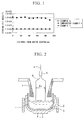
- Ni contamination of 1 ⁇ 10 13 atoms/cm 2 was conducted relative to the surface of the aforementioned silicon wafer of example 1, and after conducting heat treatment of 900°C x 30 min in a furnace with a nitrogen atmosphere, light etching was conducted for 2 minutes, and etching pits (etching pit density) that had arisen on the wafer surface were measured. These etching pits are Ni silicide which arises on the wafer surface in the case where the gettering effect is insufficient. The results are shown by the ⁇ marks in Fig. 1 .
- a silicon wafer (with an initial oxygen concentration of 12.1-13.2 x 10 17 atoms/cc (old-ASTM)) sliced from a silicon monocrystal ingot with a diameter of 200 mm was subjected to heat treatment in a non-oxidizing atmosphere under conditions of a heat treatment temperature of 1200°C, a heat treatment time of 2 hours, a rate of temperature increase of 7.5°C/min within a temperature range of 700°C-1000°C, and a rate of temperature increase of 1°C/min within a temperature range of 1000°C-1200°C during the heat treatment process.
- This post-heat treatment silicon wafer (hereinafter referred to as the silicon wafer of example 2) was observed by transmission electron microscope, and it was confirmed whether or not punch-out dislocations from bulk micro defects (BMD) had occurred. As shown in Table 1, the occurrence of punch-out dislocations was not observed.
- this silicon wafer of example 2 was repeatedly subjected 3 times to the rapid-temperature- increase/decrease heat treatment conducted in device manufacturing processes under conditions of a maximum temperature of 1150°C and a rate of temperature increase of 300°C/sec. It was subsequently observed by X-ray topography observation whether there existed slip dislocations with movement toward the wafer surface, but the occurrence of slip dislocations was not observed.
- Ni contamination of I ⁇ 10 13 atoms/cm 2 was conducted relative to the surface of the aforementioned silicon wafer of example 2, and after conducting heat treatment of 900°C x 30 min in a furnace with a nitrogen atmosphere, light etching was conducted for 2 minutes, and etching pits (etching pit density) that had arisen on the wafer surface were measured. The results are shown by the 0 marks in Fig. 1 .
- a silicon wafer (with an initial oxygen concentration of 12.1-13.2 x 10 17 atoms/cc (old-ASTM)) sliced from a silicon monocrystal ingot with a diameter of 200 mm was subjected to heat treatment in a non-oxidizing atmosphere under conditions of a heat treatment temperature of 1200°C, a heat treatment time of 2 hours, a rate of temperature increase of 7.5°C/min within a temperature range of 700°C-1000°C, and a rate of temperature increase of 1°C/min within a temperature range of 1000°C-1200°C during the heat treatment process.
- This post-heat treatment silicon wafer (hereinafter referred to as the silicon wafer of example 7) was observed by transmission electron microscope, and it was confirmed whether or not punch-out dislocations from bulk micro defects (BMD) had occurred. As shown in Table 1, the occurrence of punch-out dislocations was not observed.
- this silicon wafer of example 7 was repeatedly subjected 3 times to the rapid-temperature-increase/decrease heat treatment (flash-lamp annealing) conducted in device manufacturing processes under conditions of a maximum temperature of 1200°C and a rate of temperature increase of 250000°C/sec. It was subsequently observed by X-ray topography observation whether there existed slip dislocations with movement toward the wafer surface, but the occurrence of slip dislocations was not observed.
- flash-lamp annealing flash-lamp annealing
- a silicon wafer (with an initial oxygen concentration of 12.1-13.2 x 10 17 atoms/cc (old-ASTM)) sliced from a silicon monocrystal ingot with a diameter of 200 mm was subjected to heat treatment in a non-oxidizing atmosphere under conditions of a heat treatment temperature of 1200°C, a heat treatment time of 1 hour, a rate of temperature increase of 7.5°C/min within a temperature range of 700°C-1000°C, and a rate of temperature increase of 1°C/min within a temperature range of 1000°C-1200°C during the heat treatment process.
- This post-heat treatment silicon wafer (hereinafter referred to as the silicon wafer of comparative example 1) was observed by transmission electron microscope, and it was confirmed whether or not punch-out dislocations from bulk micro defects (BMD) had occurred. As shown in Table 1, the occurrence of punch-out dislocations was not observed.
- this silicon wafer of comparative example 1 was repeatedly subjected 3 times to the rapid-temperature-increase/decrease heat treatment conducted in device manufacturing processes under conditions of a maximum temperature of 1150°C and a rate of temperature increase of 300°C/sec.
- a maximum temperature of 1150°C 1150°C
- a rate of temperature increase of 300°C/sec 3°C/sec.
- a silicon wafer (with an initial oxygen concentration of 12.1-13.2 x 10 17 atoms/cc (old-ASTM)) sliced from a silicon monocrystal ingot with a diameter of 200 mm was subjected to heat treatment in a non-oxidizing atmosphere under conditions of a heat treatment temperature of 1200°C. a heat treatment time of 0.5 hour, a rate of temperature increase of 7.5°C/min within a temperature range of 700°C-1000°C, and a rate of temperature increase of 1°C/min within a temperature range of 1000°C-1200°C during the heat treatment process.
- This post-heat treatment silicon wafer (hereinafter referred to as the silicon wafer of comparative example 2) was observed by transmission electron microscope, and it was confirmed whether or not punch-out dislocations from bulk micro defects (BMD) had occurred. As shown in Table 1, the occurrence of punch-out dislocations was not observed.
- this silicon wafer of comparative example 2 was repeatedly subjected 3 times to the rapid-temperature-increase/decrease heat treatment conducted in device manufacturing processes under conditions of a maximum temperature of 1 150°C and a rate of temperature increase of 300°C/sec.
- a maximum temperature of 1 150°C and a rate of temperature increase of 300°C/sec.
- a silicon wafer (with an initial oxygen concentration of 12.1-13.2 x 10 17 atoms/cc (old-ASTM)) sliced from a silicon monocrystal ingot with a diameter of 200 mm was subjected to heat treatment in a non-oxygenated atmosphere under conditions of a heat treatment temperature of 1200°C, a heat treatment time of 1 hour, a rate of temperature increase of 7.5°C/min within a temperature range of 700°C-1000°C, and a rate of temperature increase of 1°C/min within a temperature range of 1000°C-1200°C during the heat treatment process.
- This post-heat treatment silicon wafer (hereinafter referred to as the silicon wafer of comparative example 3) was observed by transmission electron microscope, and it was confirmed whether or not punch-out dislocations from bulk micro defects (BMD) had occurred. As shown in Table 1, the occurrence of punch-out dislocations was not observed.
- this silicon wafer of comparative example 3 was repeatedly subjected 3 times to the rapid-temperature-increase/decrease heat treatment conducted in device manufacturing processes under conditions of a maximum temperature of 1 100°C and a rate of temperature increase of 300°C/sec.
- a maximum temperature of 1 100°C 100°C
- a rate of temperature increase of 300°C/sec 300°C/sec.
- a silicon wafer (with an initial oxygen concentration of 9.6-10.3 ⁇ 10 17 atoms/cc (old-ASTM)) sliced from a silicon monocrystal ingot with a diameter of 200 mm was subjected to heat treatment in a non-oxidizing atmosphere under conditions of a heat treatment temperature of 1200°C, a heat treatment time of 2 hours, a rate of temperature increase of 7.5°C/min within a temperature range of 700°C-1000°C, and a rate of temperature increase of 1°C/min within a temperature range of 1000°C-1200°C during the heat treatment process.
- This post-heat treatment silicon wafer (hereinafter referred to as the silicon wafer of comparative example 4) was observed by transmission electron microscope, and it was confirmed whether or not punch-out dislocations from bulk micro defects (BMD) had occurred. As shown in Table 1, the occurrence of punch-out dislocations was not observed.
- this silicon wafer of comparative example 4 was repeatedly subjected 3 times to the rapid-temperature-increase/decrease heat treatment conducted in device manufacturing processes under conditions of a maximum temperature of 1150°C and a rate of temperature increase of 300°C/sec.
- a maximum temperature of 1150°C 1150°C
- a rate of temperature increase of 300°C/sec 3°C/sec.
- Ni contamination of 1 x 10 13 atoms/cm 2 was conducted relative to the surface of the aforementioned silicon wafer of comparative example 4, and after conducting heat treatment of 900°C x 30 min in a furnace with a nitrogen atmosphere, light etching was conducted for 2 minutes, and etching pits (etching pit density) that had arisen on the wafer surface were measured. The results are shown by the O marks in Fig. 1 .
- a silicon wafer (with an initial oxygen concentration of 12.1-13.2 x 10 17 atoms/cc (old-ASTM)) sliced from a silicon monocrystal ingot with a diameter of 200 mm was subjected to heat treatment in a non-oxidizing atmosphere under conditions of a heat treatment temperature of 1200°C, a heat treatment time of 1 hour, a rate of temperature increase of 7.5°C/min within a temperature range of 700°C-1000°C, and a rate of temperature increase of 1°C/min within a temperature range of 1000°C-1200°C during the heat treatment process.
- This post-heat treatment silicon wafer (hereinafter referred to as the silicon wafer of reference example 1) was observed by transmission electron microscope, and it was confirmed whether or not punch-out dislocations from bulk micro defects (BMD) had occurred. As shown in Table 1, the occurrence of punch-out dislocations was not observed.
- this silicon wafer of reference example 1 was repeatedly subjected 3 times to the rapid-temperature-increase/decrease heat treatment conducted in device manufacturing processes under conditions of a maximum temperature of 1075°C and a rate of temperature increase of 300°C/sec.
- a maximum temperature of 1075°C 1075°C
- a rate of temperature increase of 300°C/sec 300°C/sec.
- a silicon wafer (with an initial oxygen concentration of 12.1-13.2 x 10 17 atoms/cc (old-ASTM)) sliced from a silicon monocrystal ingot with a diameter of 200 mm was subjected to heat treatment in a non-oxidizing atmosphere under conditions of a heat treatment temperature of 1200°C, a heat treatment time of 3 hours, a rate of temperature increase of 7.5°C/min within a temperature range of 700°C-1000°C, and a rate of temperature increase of 1°C/min within a temperature range of 1000°C-1200°C during the heat treatment process.
- This post-heat treatment silicon wafer (hereinafter referred to as the silicon wafer of reference example 2) was observed by transmission electron microscope, and it was confirmed whether or not punch-out dislocations from bulk micro defects (BMD) had occurred. As shown in Table 1. the occurrence of punch-out dislocations was observed.
- this silicon wafer of reference example 2 was repeatedly subjected 3 times to the rapid-temperature-increase/decrease heat treatment conducted in device manufacturing processes under conditions of a maximum temperature of 1075°C and a rate of temperature increase of 300°C/sec.
- a maximum temperature of 1075°C 1075°C
- a rate of temperature increase of 300°C/sec 300°C/sec.
- a silicon wafer (with an initial oxygen concentration of 12.1-13.2 x 10 17 atoms/cc (old-ASTM)) sliced from a silicon monocrystal ingot with a diameter of 200 mm was subjected to heat treatment in a non-oxidizing atmosphere under conditions of a heat treatment temperature of 1200°C, a heat treatment time of 1 hour, a rate of temperature increase of 7.5°C/min within a temperature range of 700°C-1000°C, and a rate of temperature increase of 1°C/min within a temperature range of 1000°C-1200°C during the heat treatment process.
- This post-heat treatment silicon wafer (hereinafter referred to as the silicon wafer of reference example 3) was observed by transmission electron microscope, and it was confirmed whether or not punch-out dislocations from bulk micro defect (BMD) had occurred. As shown in Table 1, the occurrence of punch-out dislocations was not observed.
- this silicon wafer of reference example 3 was repeatedly subjected 3 times to the rapid-temperature-increase/decrease heat treatment conducted in device manufacturing processes under conditions of a maximum temperature of 1 100°C and a rate of temperature increase of 230°C/sec.
- a maximum temperature of 1 100°C 100°C
- a rate of temperature increase of 230°C/sec a rate of temperature increase of 230°C/sec.
- a silicon wafer (with an initial oxygen concentration of 12.1-13.2 x 10 17 atoms/cc (old-ASTM)) sliced from a silicon monocrystal ingot with a diameter of 200 mm was subjected to heat treatment in a non-oxidizing atmosphere under conditions of a heat treatment temperature of 1200°C, a heat treatment time of 1 hour, a rate of temperature increase of 7.5°C/min within a temperature range of 700°C-1000°C, and a rate of temperature increase of 1°C/min within a temperature range of 1000°C-1200°C during the heat treatment process.
- This post-heat treatment silicon wafer (hereinafter referred to as the silicon wafer of reference example 4) was observed by transmission electron microscope, and it was confirmed whether or not punch-out dislocations from bulk micro defects (BMD) had occurred. As shown in Table 1, the occurrence of punch-out dislocations was not observed.
- this silicon wafer of reference example 4 was repeatedly subjected 3 times to the rapid-temperature-increase/decrease heat treatment conducted in device manufacturing processes under conditions of a maximum temperature of 1100°C and a rate of temperature increase of 250°C/sec.
- a maximum temperature of 1100°C 1100°C
- a rate of temperature increase of 250°C/sec 2°C/sec
- Grown-in defects signify microdefects which become evident in the manufacturing process of the device and which greatly affect its performance; these are defects whose causes develop during the monocrystal growth phase.
- the "silicon monocrystal ingot grown... so as to be free of grown-in defects in the body portion" pertaining to the present invention may be obtained, for example, by a silicon monocrystal growth method according to the Czochralski method, which is a growth method that conducts pulling up within a prescribed range of speed and that sets intracrystalline temperature distribution immediately after solidification during pulling up (temperature distribution in the pull direction; a distribution within a temperature range from the melting point to 1250°C) so that the crystal periphery (Ge) is smaller than the crystal center (Gc) (Gc > Ge).
- the Czochralski method is a growth method that conducts pulling up within a prescribed range of speed and that sets intracrystalline temperature distribution immediately after solidification during pulling up (temperature distribution in the pull direction; a distribution within a temperature range from the melting point to 1250°C) so that the crystal periphery (Ge) is smaller than the crystal center (Gc) (Gc > Ge).
- the pulling up speed of prescribed range that serves to obtain monocrystal free of grown-in defects varies according to the hot zone structure which satisfies the bore diameter of the monocrystal and a temperature distribution of Gc > Ge.
- the speed range is constant. Consequently, it is acceptable to initially grow monocrystal with continual changing of pulling up speed, and to study and select the speed range based thereon.
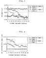
- a thermal shield 7 is structured so that its shell is made from graphite, and its interior is filled with graphite felt.
- This growth apparatus is set so that temperature distribution in the crystal satisfies Gc ⁇ Ge when the monocrystal pulled up from the melt is within a temperature range from the melting point to 1250°C.
- High-purity silicon polycrystal was inserted into a crucible 1, a reduced-pressure atmosphere was created inside the apparatus, and the silicon was melted by heating with a heater 2 to obtain a melt 3. Seed crystal attached to a seed chuck 5 was immersed in the melt 3, and pull-up was conducted while rotating the crucible 1 and a pull-up shaft 4. After conducting seed contraction in order to obtain dislocation-free crystal, the shoulder portion was formed, and - transitioning from the shoulder - the body portion was formed.
- the target diameter Dc of the body portion is set at 200 mm.
- the central portion was set to 3.0-3.2°C/mm and the peripheral portion to 2.3-2.5°C/mm, and the monocrystal was grown by having pull-up speed undergo a change of 0.6 mm/min ⁇ 0.3 mm/min ⁇ 0.6 mm/min.
- Oxygen concentration was 11.4-12.6 x 10 17 atoms/cc (old ASTM).
- the obtained monocrystal was sliced, and the wafer excised from the area grown as the interstitial-silicon-dominant defect-free region was used as the wafer of example 3.
- the wafer was subjected to heat treatment of 800°C x 4 hours and 1000°C x 16 hours in a dry oxygen atmosphere, 2 ⁇ m of light etching was conducted after cleaving the wafer, and the density of the oxygen precipitate was measured.
- a region where oxygen precipitate density of 5 x 10 4 /cm 2 or less was observed was considered as an interstitial-silicon-dominant defect-free region, and a region where bulk micro defect density in excess of 5 x 10 4 /cm 2 was observed was considered as a vacancy-dominant defect-free region.
- the density distribution of bulk micro defects (BMD) in the radial direction of the wafer is shown by the O marks in Fig. 3 , and it was confirmed that the wafer of example 3 was an interstitial-silicon-dominant defect-free wafer with an oxygen precipitate density of approximately 1 x 10 4 /cm 2 across the entire surface in the radial direction.
- the defect-free properties in the depthwise direction of the wafer of example 3 was evaluated by the 90° light scattering method using MO-441 manufactured by Mitsui Kinzoku Co. Ltd.
- This measurement of light scattering defects (light scattering bodies) by the 90° light scattering method was conducted by the incidence of light of 1.06 ⁇ m (near infrared) wavelength of 1 W output from the surface side of the silicon wafer, and the detection of 90° scattered light detected from the cleaved surface of the wafer.
- the 90° scattered light was attenuated by insertion of a filter.
- this silicon wafer of example 3 was repeatedly subjected 3 times to the rapid-temperature-increase/decrease heat treatment conducted in device manufacturing processes under conditions of a maximum temperature of 1 100°C and a rate of temperature increase of 300°C/sec. It was subsequently observed by X-ray topography observation whether there existed slip dislocations with movement toward the wafer surface, but the occurrence of slip dislocations was not observed.
- a silicon wafer identical to that of example 3 was repeatedly subjected 3 times to the rapid-temperature-increase/decrease heat treatment conducted in device manufacturing processes under conditions of a maximum temperature of 1150°C and a rate of temperature increase of 300°C/sec. It was subsequently observed by X-ray topography observation whether there existed slip dislocations with movement toward the wafer surface, but the occurrence of slip dislocations was not observed.
- the monocrystal obtained in example 3 was sliced, and a wafer excised from a location where a vacancy-dominant defect-free region and an interstitial-silicon-dominant defect-free region intermixed was used as the wafer of example 5.
- the wafer was subjected to heat treatment of 800°C x 4 hours and 1000°C x 16 hours in a dry oxygen atmosphere, 2 ⁇ m of light etching was conducted after cleaving the wafer, and the density of the bulk micro defect was measured.
- a region where bulk micro defect density of 5 ⁇ 10 4 /cm 2 or less was observed was considered as an interstitial-silicon-dominant defect-free region, and a region where bulk micro defect density in excess of 5 x 10 4 /cm 2 was observed was considered as a vacancy-dominant defect-free region.
- the density distribution of bulk micro defects (BMD) in the radial direction of the wafer is shown by the 0 marks in Fig. 3 , and it was confirmed that the wafer of example 5 was a wafer which had a vacancy-dominant defect-free region from the wafer center to 30 mm and which, outside of this, had an interstitial-silicon-dominant defect-free region with an oxygen precipitate density of approximately 1 x 10 4 /cm 2 .
- Defect-free properties in the depthwise direction of the wafer of example 5 was evaluated by the 90° light scattering method using MO-441 manufactured by Mitsui Kinzoku Co. Ltd. in the same manner as example 3. These measurement results are shown by the 0 marks in Fig. 4 , and it was confirmed that the wafer of example 5 was a defect-free wafer with a light scattering defect density of approximately 2 x 10 5 /cm 3 or less in the region at a depth of 50-310 ⁇ m across the entire surface in the radial direction.
- this silicon wafer of example 5 was repeatedly subjected 3 times to the rapid-temperature-increase/decrease heat treatment conducted in device manufacturing processes under conditions of a maximum temperature of 1 100°C and a rate of temperature increase of 300°C/sec. It was subsequently observed by X-ray topography observation whether there existed slip dislocations with movement toward the wafer surface, but the occurrence of slip dislocations was not observed.
- a silicon wafer identical to that of example 5 was repeatedly subjected 3 times to the rapid-temperature-increase/decrease heat treatment conducted in device manufacturing processes under conditions of a maximum temperature of 1150°C and a rate of temperature increase of 300°C/sec. It was subsequently observed by X-ray topography observation whether there existed slip dislocations with movement toward the wafer surface, but the occurrence of slip dislocations was not observed.
- a silicon wafer identical to that of example 3 and example 5 was repeatedly subjected 3 times to the rapid-temperature-increase/decrease heat treatment (flash-lamp annealing) conducted in device manufacturing processes under conditions of a maximum temperature of 1200°C and a rate of temperature increase of 250000°C/sec. It was subsequently observed by X-ray topography observation whether there existed slip dislocations with movement toward the wafer surface, but the occurrence of slip dislocations was not observed.
- flash-lamp annealing flash-lamp annealing
- the monocrystal obtained in example 3 was sliced, and a wafer excised from a location grown as a vacancy-dominant defect-free region was used as the wafer of comparative example 5.
- the wafer was subjected to heat treatment of 800°C x 4 hours and 1000°C x 16 hours in a dry oxygen atmosphere, 2 ⁇ m of light etching was conducted after cleaving the wafer, and the density of the bulk micro defect was measured.
- a region where bulk micro defect density of 5 ⁇ 10 4 /cm 2 or less was observed was considered as an interstitial-silicon-dominant defect-free region, and a region where oxygen precipitate density in excess of 5 x 10 4 /cm 2 was observed was considered as a vacancy-dominant defect-free region.
- the density distribution of bulk micro defects (BMD) in the radial direction of the wafer is shown by the ⁇ marks in Fig. 3 , and it was confirmed that the wafer of comparative example 5 was a vacancy-dominant defect-free wafer with an oxygen precipitate density of approximately 1 x 10 6 /cm 2 across the entire surface in the radial direction.
- the defect-free properties in the depthwise direction of the wafer of comparative example 5 was evaluated by the 90° light scattering method using MO-441 manufactured by Mitsui Kinzoku Co. Ltd. in the same manner as example 3. These measurement results are shown by the ⁇ marks in Fig. 4 , and it was confirmed that the wafer of comparative example 5 was a wafer with a light scattering defect density of approximately 4 x 10 5 /cm 3 or more in the region at a depth of 50-310 ⁇ m across the entire surface in the radial direction.
- this silicon wafer of comparative example 5 was repeatedly subjected 3 times to the rapid-temperature-increase/decrease heat treatment conducted in device manufacturing processes under conditions of a maximum temperature of 1 100°C and a rate of temperature increase of 300°C/sec.
- a maximum temperature of 1 100°C 100°C
- a rate of temperature increase of 300°C/sec 300°C/sec.
- a silicon wafer identical to comparative example 5 was repeatedly subjected 3 times to the rapid-temperature-increase/decrease heat treatment conducted in device manufacturing processes under conditions of a maximum temperature of 1 150°C and a rate of temperature increase of 300°C/sec.
- a maximum temperature of 1 150°C and a rate of temperature increase of 300°C/sec.
- the monocrystal obtained in example 3 was sliced, and a wafer excised from a location where a vacancy-dominant defect-free region and an interstitial-silicon-dominant defect-free region intermixed was used as the wafer of comparative example 7.
- the wafer was subjected to heat treatment of 800°C x 4 hours and 1000°C x 16 hours in a dry oxygen atmosphere, 2 ⁇ m of light etching was conducted after cleaving the wafer, and the density of the bulk micro defect was measured.
- a region where bulk micro defect density of 5 x 10 4 /cm 2 or less was observed was considered as an interstitial-silicon-dominant defect-free region, and a region where bulk micro defect density in excess of 5 ⁇ 10 4 /cm 2 was observed was considered as a vacancy-dominant defect-free region.
- the density distribution of bulk micro defects (BMD) in the radial direction of the wafer is shown by the ⁇ marks in Fig. 3 , and it was confirmed that the wafer of comparative example 7 was a wafer which had a vacancy-dominant defect-free region from the wafer center to 60 mm and which, outside of this, had an interstitial-silicon-dominant defect-free region with an bulk micro defect density of approximately 1 x 10 4 /cm 2 .
- the defect-free properties in the depthwise direction of the wafer of comparative example 7 was evaluated by the 90° light scattering method using MO-441 manufactured by Mitsui Kinzoku Co. Ltd. in the same manner as example 3. These measurement results are shown by the ⁇ marks in Fig. 4 , and it was observed that the wafer of comparative example 7 had a light scattering defect density of 2 x 10 5 /cm 3 or more in the region from the wafer center until 35 mm.
- this silicon wafer of example 7 was repeatedly subjected 3 times to the rapid-temperature-increase/decrease heat treatment conducted in device manufacturing processes under conditions of a maximum temperature of I 100°C and a rate of temperature increase of 300°C/sec.
- a maximum temperature of I 100°C and a rate of temperature increase of 300°C/sec.
- a silicon wafer identical to comparative example 7 was repeatedly subjected 3 times to the rapid-temperature-increase/decrease heat treatment conducted in device manufacturing processes under conditions of a maximum temperature of I 150°C and a rate of temperature increase of 300°C/sec.
- a maximum temperature of I 150°C and a rate of temperature increase of 300°C/sec.
- the silicon wafer of example 3 was repeatedly subjected 3 times to the rapid-temperature-increase/decrease heat treatment conducted in device manufacturing processes under conditions of a maximum temperature of 1075°C and a rate of temperature increase of 300°C/sec. It was subsequently observed by X-ray topography observation whether there existed slip dislocations with movement toward the wafer surface, but the occurrence of slip dislocations was not observed.
- the silicon wafer of example 5 was repeatedly subjected 3 times to the rapid-temperature-increase/decrease heat treatment conducted in device manufacturing processes under conditions of a maximum temperature of 1075°C and a rate of temperature increase of 300°C/sec. It was subsequently observed by X-ray topography observation whether there existed slip dislocations with movement toward the wafer surface, but the occurrence of slip dislocations was not observed.
- the silicon wafer of example 5 was repeatedly subjected 3 times to the rapid-temperature-increase/decrease heat treatment conducted in device manufacturing processes under conditions of a maximum temperature of 1 100°C and a rate of temperature increase of 250°C/sec. It was subsequently observed by X-ray topography observation whether there existed slip dislocations with movement toward the wafer surface, but the occurrence of slip dislocations was not observed.
- the silicon wafer of comparative example 5 was repeatedly subjected 3 times to the rapid-temperature-increase/decrease heat treatment conducted in device manufacturing processes under conditions of a maximum temperature of 1075°C and a rate of temperature increase of 300°C/sec. It was subsequently observed by X-ray topography observation whether there existed slip dislocations with movement toward the wafer surface, but the occurrence of slip dislocations was not observed.
- the silicon wafer of comparative example 5 was repeatedly subjected 3 times to the rapid-temperature-increase/decrease heat treatment conducted in device manufacturing processes under conditions of a maximum temperature of 1100°C and a rate of temperature increase of 250°C/sec. It was subsequently observed by X-ray topography observation whether there existed slip dislocations with movement toward the wafer surface, but the occurrence of slip dislocations was not observed.
- the silicon wafer of comparative example 7 was repeatedly subjected 3 times to the rapid-temperature-increase/decrease heat treatment conducted in device manufacturing processes under conditions of a maximum temperature of 1075°C and a rate of temperature increase of 300°C/sec. It was subsequently observed by X-ray topography observation whether there existed slip dislocations with movement toward the wafer surface, but the occurrence of slip dislocations was not observed.
Landscapes
- Crystals, And After-Treatments Of Crystals (AREA)
Abstract
Description
- The present invention relates to a silicon wafer suited for use in a semiconductor device manufacturing process which conducts heat treatment at a maximum temperature of 1100°C or more and at a rate of temperature increase of 300°C/sec or more after the silicon wafer which is the base material of the device has undergone a mirror machining process, and to a manufacturing method thereof.
- Priority is claimed on Japanese Patent Application No.
2007-036630, filed February 16, 2007 - Due to the ever higher integration of devices, furnaces exhibiting rapid temperature increases and decreases have come into frequent use in device manufacturing processes (see Patent Reference 1), and their maximum temperatures are also trending upward. In particular, in the case of unilateral heating inside furnaces exhibiting rapid temperature increases and decreases, it happens - although for a very short time - that a large temperature disparity occurs between the front face and rear face of the wafer.
- When a large temperature disparity occurs between the front and rear faces in this manner even for a short time, it has been found that slip dislocations may occur from the oxygen precipitate existing in the vicinity of surface layer of the wafer, which may move to the surface layer of the wafer (the active layer side of the device), and penetrate the surface.
- Moreover, when punch-out dislocations which arise from oxygen precipitate before heat treatment involving rapid temperature increase/decrease and when dislocation clusters which are aggregates of interstitial silicon exist in the wafer, high stress is sustained, slip dislocations occur, and the surface layer of the wafer is penetrated. When such dislocations exist in the active layer of the device, they cause leak defects in the device, and degrade device yield.
- Patent Reference 1: Japanese Unexamined Patent Application, First Publication No.
2006-310690 - The problem that the present invention is to solve is to provide a silicon wafer which achieves a gettering effect without occurrence of slip dislocations even when heat treatment is conducted at a maximum temperature of 1 100°C or more and at a rate of temperature increase of 300°C/sec or more after the silicon wafer has undergone a mirror machining process.
- With respect to the first aspect of the present invention, after slicing from a silicon monocrystal ingot, heat treatment is conducted so that a layer which has zero light scattering defects according to the 90° light scattering method is formed in a region at a depth from the wafer surface of 25 µm or more but less than 100 µm, and a layer which has a light scattering defect density of 1 x 10⁸/cm3 or more according to the 90° light scattering method is formed in a region at a depth of 100 µm from the wafer surface.
- The second aspect of the present invention pertains to a silicon wafer sliced from a silicon monocrystal ingot grown by the Czochralski technique so as to be free of grown-in defects in the body portion, which is a silicon wafer used in a semiconductor device manufacturing process which conducts heat treatment under conditions of a maximum temperature of 1 100°C or more and a rate of temperature increase of 300°C/sec or more after subjecting the silicon wafer to mirror machining, wherein a layer which has a light scattering defect density of 2 × 105 cm3 or less according to the 90° light scattering method is formed in a region at a depth of 50 µm or more from the wafer surface.
- According to the first aspect of the present invention, as a layer which has zero light scattering defects according to the 90° light scattering method is formed in a region at a depth from the wafer surface (active layer side of the device) of 25 µm or more but less than 100 µm, slip dislocations do not occur even when heat treatment is conducted at a maximum temperature of 1100°C or more and at a rate of temperature increase of 300°C/sec or more after the silicon wafer has undergone a mirror machining process.
- In addition, as a layer which has a light scattering defect density of I x 108/cm3 or more according to the 90° light scattering method is formed in a region at a depth of 100 µm from the wafer surface, a gettering effect relative to heavy metal contaminants is obtained.
- According to the second aspect of the present invention, as a layer which has a light scattering defect density of 2 × 105 cm3 or less according to the 90° light scattering method is formed in a region at a depth of 50 µm or more from the wafer surface, slip dislocations do not occur even when heat treatment is conducted at a maximum temperature of 1 100°C or more and at a rate of temperature increase of 300°C/sec or more after the silicon wafer has undergone a mirror machining process.
-
-
Fig. 1 is a graph which shows results confirming a gettering effect by the present invention. -
Fig. 2 is a schematic diagram which shows an example of configuration of a silicon monocrystal growth apparatus used in the examples. -
Fig. 3 is a graph which shows the density distribution of bulk micro defects of examples 3 and 5 and comparative examples 5 and 7. -
Fig. 4 is a graph which shows the density distribution of light scattering defects of examples 3 and 5 and comparative examples 5 and 7. - (1)The invention according to the first aspect
When a wafer which has been sliced from a silicon monocrystal ingot is subjected to heat treatment so that a layer which has zero light scattering defects according to the 90° light scattering method is formed in a region at a depth from the wafer surface of 25 µm or more but less than 100 µm, and a layer which has a light scattering defect density of 1 x 10⁸/cm3 or more according to the 90° light scattering method is formed in a region at a depth of 100 µm from the wafer surface, it was confirmed in conjunction with comparative examples and reference examples that slip dislocations do not occur and that a gettering effect is obtained with such heat treated wafers even when they are subjected to heat treatment under conditions of a maximum temperature of 1 100°C or more and a rate of temperature increase of 300°C/sec or more in a semiconductor device manufacturing process. - In order to distinguish between the heat treatment conducted in the semiconductor device manufacturing process and the heat treatment conducted in the silicon wafer manufacturing process, the heat treatment conducted in the semiconductor device manufacturing process is specifically referred to as rapid-temperature-increase/decrease heat treatment in the following description.
- A silicon wafer (with an initial oxygen concentration of 10.8-11.9 × 10¹⁷ atoms/cc (old-ASTM)) sliced from a silicon monocrystal ingot with a diameter of 200 mm was subjected to heat treatment in a non-oxidizing atmosphere under conditions of a heat treatment temperature of 1200°C, a heat treatment time of 2 hours, a rate of temperature increase of 7.5°C/min within a temperature range of 700°C-1000°C, and a rate of temperature increase of 1°C/min within a temperature range of 1000°C-1200°C during the heat treatment process.
- This post-heat treatment silicon wafer (hereinafter referred to as the silicon wafer of example 1) was observed by transmission electron microscope, and it was confirmed whether or not punch-out dislocations from bulk micro defects (BMD) had occurred. As shown in Table 1, the occurrence of punch-out dislocations was not observed.
- Moreover, completeness in the vicinity of the surface layer of the post-heat treatment silicon wafer was evaluated by the 90° light scattering method using MO-441 manufactured by Mitsui Kinzoku Co. Ltd. Measurement of light scattering defects (light scattering bodies) by this 90° light scattering method was conducted by the incidence of light of 1.06 µm (near infrared) wavelength of 100 mW output from the surface side of the silicon wafer, and the detection of 90° scattered light detected from the cleaved surface of the wafer. The 90° scattered light was attenuated by insertion of a filter.
- The measurement region was considered as the region to a depth of 260 µm from the wafer surface, and 10 points were measured in the radial direction of the wafer with 2 mm in the diametric direction of the wafer constituting 1 view field. Based on the photographed images, measurement proceeded at the depth from the wafer surface where light scattering defects are first detected, and the depth where light scattering defects are not detected was sought. In addition, the density of light scattering defects at a depth of 100 µm was also measured.
- As a result, as shown in Table 1, it was found with respect to the wafer of example 1 that the region where light scattering defects are zero was the region at 51 µm from the wafer surface. Moreover, light scattering defect density at a depth of 100 µm from the wafer surface was 1.3 x 10⁸/cm3.
- Next, this silicon wafer of example 1 was repeatedly subjected 3 times to the rapid-temperature-increase/decrease heat treatment conducted in device manufacturing processes under conditions of a maximum temperature of 1 150°C and a rate of temperature increase of 300°C/sec. It was subsequently observed by X-ray topography observation whether there existed slip dislocations with movement toward the wafer surface, but the occurrence of slip dislocations was not observed.
- In addition, Ni contamination of 1 × 10¹³ atoms/cm2 was conducted relative to the surface of the aforementioned silicon wafer of example 1, and after conducting heat treatment of 900°C x 30 min in a furnace with a nitrogen atmosphere, light etching was conducted for 2 minutes, and etching pits (etching pit density) that had arisen on the wafer surface were measured. These etching pits are Ni silicide which arises on the wafer surface in the case where the gettering effect is insufficient. The results are shown by the □ marks in
Fig. 1 . - A silicon wafer (with an initial oxygen concentration of 12.1-13.2 x 10¹⁷ atoms/cc (old-ASTM)) sliced from a silicon monocrystal ingot with a diameter of 200 mm was subjected to heat treatment in a non-oxidizing atmosphere under conditions of a heat treatment temperature of 1200°C, a heat treatment time of 2 hours, a rate of temperature increase of 7.5°C/min within a temperature range of 700°C-1000°C, and a rate of temperature increase of 1°C/min within a temperature range of 1000°C-1200°C during the heat treatment process.
- This post-heat treatment silicon wafer (hereinafter referred to as the silicon wafer of example 2) was observed by transmission electron microscope, and it was confirmed whether or not punch-out dislocations from bulk micro defects (BMD) had occurred. As shown in Table 1, the occurrence of punch-out dislocations was not observed.
- Moreover, when completeness in the vicinity of the surface layer of the post-heat treatment silicon wafer was evaluated by the 90° light scattering method using MO-441 manufactured by Mitsui Kinzoku Co. Ltd. in the same manner as example 1, it was found, as shown in Table 1, that the region where light scattering defects are zero was the region at 25 µm from the wafer surface. Light scattering defect density at a depth of 100 µm from the wafer surface was 2.7 x 10⁹/cm3.
- Next, this silicon wafer of example 2 was repeatedly subjected 3 times to the rapid-temperature- increase/decrease heat treatment conducted in device manufacturing processes under conditions of a maximum temperature of 1150°C and a rate of temperature increase of 300°C/sec. It was subsequently observed by X-ray topography observation whether there existed slip dislocations with movement toward the wafer surface, but the occurrence of slip dislocations was not observed.
- In addition, as in example 1, Ni contamination of I × 1013 atoms/cm2 was conducted relative to the surface of the aforementioned silicon wafer of example 2, and after conducting heat treatment of 900°C x 30 min in a furnace with a nitrogen atmosphere, light etching was conducted for 2 minutes, and etching pits (etching pit density) that had arisen on the wafer surface were measured. The results are shown by the 0 marks in
Fig. 1 . - A silicon wafer (with an initial oxygen concentration of 12.1-13.2 x 10¹⁷ atoms/cc (old-ASTM)) sliced from a silicon monocrystal ingot with a diameter of 200 mm was subjected to heat treatment in a non-oxidizing atmosphere under conditions of a heat treatment temperature of 1200°C, a heat treatment time of 2 hours, a rate of temperature increase of 7.5°C/min within a temperature range of 700°C-1000°C, and a rate of temperature increase of 1°C/min within a temperature range of 1000°C-1200°C during the heat treatment process.
- This post-heat treatment silicon wafer (hereinafter referred to as the silicon wafer of example 7) was observed by transmission electron microscope, and it was confirmed whether or not punch-out dislocations from bulk micro defects (BMD) had occurred. As shown in Table 1, the occurrence of punch-out dislocations was not observed.
- Moreover, when completeness in the vicinity of the surface layer of the post-heat treatment silicon wafer was evaluated by the 90° light scattering method using MO-441 manufactured by Mitsui Kinzoku Co. Ltd. in the same manner as example 1, it was found, as shown in Table 1, that the region where light scattering defects are zero was the region at 25 µm from the wafer surface. Light scattering defect density at a depth of 100 µm from the wafer surface was 2.7 x 10⁹/cm3.
- Next, this silicon wafer of example 7 was repeatedly subjected 3 times to the rapid-temperature-increase/decrease heat treatment (flash-lamp annealing) conducted in device manufacturing processes under conditions of a maximum temperature of 1200°C and a rate of temperature increase of 250000°C/sec. It was subsequently observed by X-ray topography observation whether there existed slip dislocations with movement toward the wafer surface, but the occurrence of slip dislocations was not observed.
- As a comparative example of examples 1 and 2, a silicon wafer (with an initial oxygen concentration of 12.1-13.2 x 10¹⁷ atoms/cc (old-ASTM)) sliced from a silicon monocrystal ingot with a diameter of 200 mm was subjected to heat treatment in a non-oxidizing atmosphere under conditions of a heat treatment temperature of 1200°C, a heat treatment time of 1 hour, a rate of temperature increase of 7.5°C/min within a temperature range of 700°C-1000°C, and a rate of temperature increase of 1°C/min within a temperature range of 1000°C-1200°C during the heat treatment process.
- This post-heat treatment silicon wafer (hereinafter referred to as the silicon wafer of comparative example 1) was observed by transmission electron microscope, and it was confirmed whether or not punch-out dislocations from bulk micro defects (BMD) had occurred. As shown in Table 1, the occurrence of punch-out dislocations was not observed.
- Moreover, when completeness in the vicinity of the surface layer of the post-heat treatment silicon wafer was evaluated by the 90° light scattering method using MO-441 manufactured by Mitsui Kinzoku Co. Ltd. in the same manner as
embodiment 1, it was found, as shown in Table 1, that the region where light scattering defects are zero was the region at 19 µm from the wafer surface. Light scattering defect density at a depth of 100 µm from the wafer surface was 1.3 x 10⁹/cm3. - Next, this silicon wafer of comparative example 1 was repeatedly subjected 3 times to the rapid-temperature-increase/decrease heat treatment conducted in device manufacturing processes under conditions of a maximum temperature of 1150°C and a rate of temperature increase of 300°C/sec. When it was subsequently observed by X-ray topography observation whether there existed slip dislocations with movement toward the wafer surface, the occurrence of slip dislocations was observed.
- As a comparative example of examples 1 and 2, a silicon wafer (with an initial oxygen concentration of 12.1-13.2
x 1017 atoms/cc (old-ASTM)) sliced from a silicon monocrystal ingot with a diameter of 200 mm was subjected to heat treatment in a non-oxidizing atmosphere under conditions of a heat treatment temperature of 1200°C. a heat treatment time of 0.5 hour, a rate of temperature increase of 7.5°C/min within a temperature range of 700°C-1000°C, and a rate of temperature increase of 1°C/min within a temperature range of 1000°C-1200°C during the heat treatment process. - This post-heat treatment silicon wafer (hereinafter referred to as the silicon wafer of comparative example 2) was observed by transmission electron microscope, and it was confirmed whether or not punch-out dislocations from bulk micro defects (BMD) had occurred. As shown in Table 1, the occurrence of punch-out dislocations was not observed.
- Moreover, when completeness in the vicinity of the surface layer of the post-heat treatment silicon wafer was evaluated by the 90° light scattering method using MO-441 manufactured by Mitsui Kinzoku Co. Ltd. in the same manner as example 1, it was found, as shown in Table 1, that the region where light scattering defects are zero was the region at 9 µm from the wafer surface. Light scattering defect density at a depth of 100 µm from the wafer surface was 5.7 x 10⁸/cm3.
- Next, this silicon wafer of comparative example 2 was repeatedly subjected 3 times to the rapid-temperature-increase/decrease heat treatment conducted in device manufacturing processes under conditions of a maximum temperature of 1 150°C and a rate of temperature increase of 300°C/sec. When it was subsequently observed by X-ray topography observation whether there existed slip dislocations with movement toward the wafer surface, the occurrence of slip dislocations was observed.
- As a comparative example of examples 1 and 2, a silicon wafer (with an initial oxygen concentration of 12.1-13.2
x 1017 atoms/cc (old-ASTM)) sliced from a silicon monocrystal ingot with a diameter of 200 mm was subjected to heat treatment in a non-oxygenated atmosphere under conditions of a heat treatment temperature of 1200°C, a heat treatment time of 1 hour, a rate of temperature increase of 7.5°C/min within a temperature range of 700°C-1000°C, and a rate of temperature increase of 1°C/min within a temperature range of 1000°C-1200°C during the heat treatment process. - This post-heat treatment silicon wafer (hereinafter referred to as the silicon wafer of comparative example 3) was observed by transmission electron microscope, and it was confirmed whether or not punch-out dislocations from bulk micro defects (BMD) had occurred. As shown in Table 1, the occurrence of punch-out dislocations was not observed.
- Moreover, when completeness in the vicinity of the surface layer of the post-heat treatment silicon wafer was evaluated by the 90° light scattering method using MO-441 manufactured by Mitsui Kinzoku Co. Ltd. in the same manner as example 1, it was found, as shown in Table 1, that the region where light scattering defects are zero was the region at 16 µm from the wafer surface. Light scattering defect density at a depth of 100 µm from the wafer surface was 2.2 x 10⁹/cm3.
- Next, this silicon wafer of comparative example 3 was repeatedly subjected 3 times to the rapid-temperature-increase/decrease heat treatment conducted in device manufacturing processes under conditions of a maximum temperature of 1 100°C and a rate of temperature increase of 300°C/sec. When it was subsequently observed by X-ray topography observation whether there existed slip dislocations with movement toward the wafer surface, the occurrence of slip dislocations was observed.
- As a comparative example of examples 1 and 2, a silicon wafer (with an initial oxygen concentration of 9.6-10.3 × 10¹⁷ atoms/cc (old-ASTM)) sliced from a silicon monocrystal ingot with a diameter of 200 mm was subjected to heat treatment in a non-oxidizing atmosphere under conditions of a heat treatment temperature of 1200°C, a heat treatment time of 2 hours, a rate of temperature increase of 7.5°C/min within a temperature range of 700°C-1000°C, and a rate of temperature increase of 1°C/min within a temperature range of 1000°C-1200°C during the heat treatment process.
- This post-heat treatment silicon wafer (hereinafter referred to as the silicon wafer of comparative example 4) was observed by transmission electron microscope, and it was confirmed whether or not punch-out dislocations from bulk micro defects (BMD) had occurred. As shown in Table 1, the occurrence of punch-out dislocations was not observed.
- Moreover, when completeness in the vicinity of the surface layer of the post-heat treatment silicon wafer was evaluated by the 90° light scattering method using MO-441 manufactured by Mitsui Kinzoku Co. Ltd. in the same manner as example 1, it was found, as shown in Table 1, that the region where light scattering defects are zero was the region at 91 µm from the wafer surface. Light scattering defect density at a depth of 100 µm from the wafer surface was 2.7 x 10⁷/cm3.
- Next, this silicon wafer of comparative example 4 was repeatedly subjected 3 times to the rapid-temperature-increase/decrease heat treatment conducted in device manufacturing processes under conditions of a maximum temperature of 1150°C and a rate of temperature increase of 300°C/sec. When it was subsequently observed by X-ray topography observation whether there existed slip dislocations with movement toward the wafer surface, the occurrence of slip dislocations was not observed.
- In addition, as in example 1, Ni contamination of 1 x 10¹³ atoms/cm2 was conducted relative to the surface of the aforementioned silicon wafer of comparative example 4, and after conducting heat treatment of 900°C x 30 min in a furnace with a nitrogen atmosphere, light etching was conducted for 2 minutes, and etching pits (etching pit density) that had arisen on the wafer surface were measured. The results are shown by the O marks in
Fig. 1 . - As a reference example of example 1 and 2 and comparative examples 1-4, a silicon wafer (with an initial oxygen concentration of 12.1-13.2
x 1017 atoms/cc (old-ASTM)) sliced from a silicon monocrystal ingot with a diameter of 200 mm was subjected to heat treatment in a non-oxidizing atmosphere under conditions of a heat treatment temperature of 1200°C, a heat treatment time of 1 hour, a rate of temperature increase of 7.5°C/min within a temperature range of 700°C-1000°C, and a rate of temperature increase of 1°C/min within a temperature range of 1000°C-1200°C during the heat treatment process. - This post-heat treatment silicon wafer (hereinafter referred to as the silicon wafer of reference example 1) was observed by transmission electron microscope, and it was confirmed whether or not punch-out dislocations from bulk micro defects (BMD) had occurred. As shown in Table 1, the occurrence of punch-out dislocations was not observed.
- Moreover, when completeness in the vicinity of the surface layer of the post-heat treatment silicon wafer was evaluated by the 90° light scattering method using MO-441 manufactured by Mitsui Kinzoku Co. Ltd. in the same manner as example 1, it was found, as shown in Table 1, that the region where light scattering defects are zero was the region at 17 µm from the wafer surface. Light scattering defect density at a depth of 100 µm from the wafer surface was 1.9 x 10⁹/cm3.
- Next, this silicon wafer of reference example 1 was repeatedly subjected 3 times to the rapid-temperature-increase/decrease heat treatment conducted in device manufacturing processes under conditions of a maximum temperature of 1075°C and a rate of temperature increase of 300°C/sec. When it was subsequently observed by X-ray topography observation whether there existed slip dislocations with movement toward the wafer surface, the occurrence of slip dislocations was not observed.
- As a reference example of examples 1 and 2 and comparative examples 1-4, a silicon wafer (with an initial oxygen concentration of 12.1-13.2
x 1017 atoms/cc (old-ASTM)) sliced from a silicon monocrystal ingot with a diameter of 200 mm was subjected to heat treatment in a non-oxidizing atmosphere under conditions of a heat treatment temperature of 1200°C, a heat treatment time of 3 hours, a rate of temperature increase of 7.5°C/min within a temperature range of 700°C-1000°C, and a rate of temperature increase of 1°C/min within a temperature range of 1000°C-1200°C during the heat treatment process. - This post-heat treatment silicon wafer (hereinafter referred to as the silicon wafer of reference example 2) was observed by transmission electron microscope, and it was confirmed whether or not punch-out dislocations from bulk micro defects (BMD) had occurred. As shown in Table 1. the occurrence of punch-out dislocations was observed.
- Moreover, when completeness in the vicinity of the surface layer of the post-heat treatment silicon wafer was evaluated by the 90° light scattering method using MO-441 manufactured by Mitsui Kinzoku Co. Ltd. in the same manner as example 1, it was found, as shown in Table 1, that the region where light scattering defects are zero was the region at 30 µm from the wafer surface. Light scattering defect density at a depth of 100 µm from the wafer surface was 4.5 x 10⁹/cm3.
- Next, this silicon wafer of reference example 2 was repeatedly subjected 3 times to the rapid-temperature-increase/decrease heat treatment conducted in device manufacturing processes under conditions of a maximum temperature of 1075°C and a rate of temperature increase of 300°C/sec. When it was subsequently observed by X-ray topography observation whether there existed slip dislocations with movement toward the wafer surface, the occurrence of slip dislocations was not observed.
- As a reference example of examples 1 and 2 and comparative examples 1-4, a silicon wafer (with an initial oxygen concentration of 12.1-13.2
x 1017 atoms/cc (old-ASTM)) sliced from a silicon monocrystal ingot with a diameter of 200 mm was subjected to heat treatment in a non-oxidizing atmosphere under conditions of a heat treatment temperature of 1200°C, a heat treatment time of 1 hour, a rate of temperature increase of 7.5°C/min within a temperature range of 700°C-1000°C, and a rate of temperature increase of 1°C/min within a temperature range of 1000°C-1200°C during the heat treatment process. - This post-heat treatment silicon wafer (hereinafter referred to as the silicon wafer of reference example 3) was observed by transmission electron microscope, and it was confirmed whether or not punch-out dislocations from bulk micro defect (BMD) had occurred. As shown in Table 1, the occurrence of punch-out dislocations was not observed.
- Moreover, when completeness in the vicinity of the surface layer of the post-heat treatment silicon wafer was evaluated by the 90° light scattering method using MO-441 manufactured by Mitsui Kinzoku Co. Ltd. in the same manner as example 1, it was found, as shown in Table 1, that the region where light scattering defects are zero was the region at 17 µm from the wafer surface. Light scattering defect density at a depth of 100 µm from the wafer surface was 1.6 x 10⁹/cm3.
- Next, this silicon wafer of reference example 3 was repeatedly subjected 3 times to the rapid-temperature-increase/decrease heat treatment conducted in device manufacturing processes under conditions of a maximum temperature of 1 100°C and a rate of temperature increase of 230°C/sec. When it was subsequently observed by X-ray topography observation whether there existed slip dislocations with movement toward the wafer surface, the occurrence of slip dislocations was not observed.
- As a reference example of examples 1 and 2 and comparative examples 1-4, a silicon wafer (with an initial oxygen concentration of 12.1-13.2
x 1017 atoms/cc (old-ASTM)) sliced from a silicon monocrystal ingot with a diameter of 200 mm was subjected to heat treatment in a non-oxidizing atmosphere under conditions of a heat treatment temperature of 1200°C, a heat treatment time of 1 hour, a rate of temperature increase of 7.5°C/min within a temperature range of 700°C-1000°C, and a rate of temperature increase of 1°C/min within a temperature range of 1000°C-1200°C during the heat treatment process. - This post-heat treatment silicon wafer (hereinafter referred to as the silicon wafer of reference example 4) was observed by transmission electron microscope, and it was confirmed whether or not punch-out dislocations from bulk micro defects (BMD) had occurred. As shown in Table 1, the occurrence of punch-out dislocations was not observed.
- Moreover, when completeness in the vicinity of the surface layer of the post-heat treatment silicon wafer was evaluated by the 90° light scattering method using MO-441 manufactured by Mitsui Kinzoku Co. Ltd. in the same manner as example 1, it was found, as shown in Table 1, that the region where light scattering defects are zero was the region at 19 µm from the wafer surface. Light scattering defect density at a depth of 100 µm from the wafer surface was 2.8 x 10⁹/cm3.
- Next, this silicon wafer of reference example 4 was repeatedly subjected 3 times to the rapid-temperature-increase/decrease heat treatment conducted in device manufacturing processes under conditions of a maximum temperature of 1100°C and a rate of temperature increase of 250°C/sec. When it was subsequently observed by X-ray topography observation whether there existed slip dislocations with movement toward the wafer surface, the occurrence of slip dislocations was not observed.
Table 1 Wafer properties Rapid heat treatment conditions Evaluation results Depth (µm) at which light scattering defects are zero Light scattering defect density (/cm3) at a depth of 100 µm Maximum temperature (°C) Rate of temperature increase (°C/sec) Slip dislocations Punch-out dislocations Gettering effect Example 1 51 1.3E+08 1150 300 No No Sufficient Example 2 25 2.7E+09 1150 300 No No Sufficient Example 7 25 2.7E+09 1200 250000 No No -- Comparative example I 19 1.3E+09 1150 300 Yes No -- Comparative example 2 9 5.7E+08 1150 300 Yes No -- Comparative example 3 16 2.2E+09 1100 300 Yes No -- Comparative example 4 91 2.7E+07 1150 300 No No Insufficient Reference example 1 17 1.9E+09 1075 300 No No -- Reference example 2 30 4.5E+09 1075 300 No Yes -- Reference example 3 18 1.6E+09 1100 230 No No -- Reference example 4 19 2.8E+09 1100 250 No No -- - From the results of comparative example 1 and reference examples 1-4, it was confirmed that when the conditions of the rapid-temperature-increase/decrease heat treatment conducted in device manufacturing processes are not those of a maximum temperature of 1 100°C or more and a rate of temperature increase of 300°C/sec or more, slip dislocations do not occur according to X-ray topography observation.
- From the results of examples 1, 2 and 7 and comparative examples 1-4 which are based thereon, it was confirmed that if a layer which has zero light scattering defects according to the 90° light scattering method is formed in a region at a depth from the wafer surface of 25 µm or more but less than 100 µm, slip dislocations do not occur even when rapid-temperature-increase/decrease heat treatment is conducted under the aforementioned conditions of a maximum temperature of 1 100°C or more and a rate of temperature increase of 300°C/sec or more.
- Moreover, from the results of examples 1, 2 and 7 and comparative example 4, it was confirmed that if a layer which has a light scattering defect density of 1 x 10⁸/cm3 or more according to the 90° light scattering method is formed in a region at a depth of 100 µm from the wafer surface, a satisfactory gettering effect is demonstrated by these light scattering defects.
- (2) The invention according to the second aspect
With respect to a silicon wafer sliced from a silicon monocrystal ingot grown by the Czochralski method so as to be free of grown-in defects in the body portion, if a layer which has a light scattering defect density of 2 × 105 cm3 or less according to the 90° light scattering method is formed in a region at a depth of 50 µm or more from the wafer surface, it was confirmed in conjunction with comparative examples and reference examples that slip dislocations do not occur even when this wafer is subjected to heat treatment under conditions of a maximum temperature of 1 100°C or more and a rate of temperature increase of 300°C/sec or more in a semiconductor device manufacturing process. - Grown-in defects signify microdefects which become evident in the manufacturing process of the device and which greatly affect its performance; these are defects whose causes develop during the monocrystal growth phase.
- The "silicon monocrystal ingot grown... so as to be free of grown-in defects in the body portion" pertaining to the present invention may be obtained, for example, by a silicon monocrystal growth method according to the Czochralski method, which is a growth method that conducts pulling up within a prescribed range of speed and that sets intracrystalline temperature distribution immediately after solidification during pulling up (temperature distribution in the pull direction; a distribution within a temperature range from the melting point to 1250°C) so that the crystal periphery (Ge) is smaller than the crystal center (Gc) (Gc > Ge).
- The pulling up speed of prescribed range that serves to obtain monocrystal free of grown-in defects varies according to the hot zone structure which satisfies the bore diameter of the monocrystal and a temperature distribution of Gc > Ge. However, if the monocrystal diameter and the pulling up apparatus remain the same, the speed range is constant. Consequently, it is acceptable to initially grow monocrystal with continual changing of pulling up speed, and to study and select the speed range based thereon.
- Using an apparatus with the sectional structure which is schematically shown in
Fig. 2 , a growth experiment was conducted with respect to asilicon monocrystal 6. In this same drawing, athermal shield 7 is structured so that its shell is made from graphite, and its interior is filled with graphite felt. - This growth apparatus is set so that temperature distribution in the crystal satisfies Gc < Ge when the monocrystal pulled up from the melt is within a temperature range from the melting point to 1250°C.
- High-purity silicon polycrystal was inserted into a
crucible 1, a reduced-pressure atmosphere was created inside the apparatus, and the silicon was melted by heating with aheater 2 to obtain amelt 3. Seed crystal attached to aseed chuck 5 was immersed in themelt 3, and pull-up was conducted while rotating thecrucible 1 and a pull-upshaft 4. After conducting seed contraction in order to obtain dislocation-free crystal, the shoulder portion was formed, and - transitioning from the shoulder - the body portion was formed. - Using a growth apparatus having the hot zone structure shown in
Fig. 2 , the target diameter Dc of the body portion is set at 200 mm. With the axial temperature gradient of the monocrystal interior during growth within a range from the melting point to 1370°C, the central portion was set to 3.0-3.2°C/mm and the peripheral portion to 2.3-2.5°C/mm, and the monocrystal was grown by having pull-up speed undergo a change of 0.6 mm/min → 0.3 mm/min → 0.6 mm/min. Oxygen concentration was 11.4-12.6x 10¹⁷ atoms/cc (old ASTM). - The obtained monocrystal was sliced, and the wafer excised from the area grown as the interstitial-silicon-dominant defect-free region was used as the wafer of example 3. To determine whether a wafer excised from the monocrystal was from an interstitial-silicon-dominant defect-free region or a vacancy-dominant defect-free region, the wafer was subjected to heat treatment of 800°C x 4 hours and 1000°C x 16 hours in a dry oxygen atmosphere, 2 µm of light etching was conducted after cleaving the wafer, and the density of the oxygen precipitate was measured. A region where oxygen precipitate density of 5 x 10⁴/cm2 or less was observed was considered as an interstitial-silicon-dominant defect-free region, and a region where bulk micro defect density in excess of 5 x 10⁴/cm2 was observed was considered as a vacancy-dominant defect-free region. The density distribution of bulk micro defects (BMD) in the radial direction of the wafer is shown by the O marks in
Fig. 3 , and it was confirmed that the wafer of example 3 was an interstitial-silicon-dominant defect-free wafer with an oxygen precipitate density of approximately 1 x 10⁴/cm2 across the entire surface in the radial direction. - Moreover, the defect-free properties in the depthwise direction of the wafer of example 3 was evaluated by the 90° light scattering method using MO-441 manufactured by Mitsui Kinzoku Co. Ltd. This measurement of light scattering defects (light scattering bodies) by the 90° light scattering method was conducted by the incidence of light of 1.06 µm (near infrared) wavelength of 1 W output from the surface side of the silicon wafer, and the detection of 90° scattered light detected from the cleaved surface of the wafer. The 90° scattered light was attenuated by insertion of a filter.
- As it is difficult with this measurement method to measure light scattering defects in the region at 50 µm from the wafer surface due to the scattering of incident light by the cleaved surface, measurement was conducted at 20 points in the radial direction of the wafer with 5 mm in the diametric direction of the wafer constituting 1 view field in the region at a depth of 50 µm to 310 µm from the wafer surface. These measurement results are shown by the O marks in
Fig. 4 , and it was confirmed that the wafer of example 3 was a defect-free wafer with a light scattering defect density of approximately 2 x 10⁵/cm3 or less in the region at a depth of 50-310 µm across the entire surface in the radial direction. - Next, this silicon wafer of example 3 was repeatedly subjected 3 times to the rapid-temperature-increase/decrease heat treatment conducted in device manufacturing processes under conditions of a maximum temperature of 1 100°C and a rate of temperature increase of 300°C/sec. It was subsequently observed by X-ray topography observation whether there existed slip dislocations with movement toward the wafer surface, but the occurrence of slip dislocations was not observed.
- A silicon wafer identical to that of example 3 was repeatedly subjected 3 times to the rapid-temperature-increase/decrease heat treatment conducted in device manufacturing processes under conditions of a maximum temperature of 1150°C and a rate of temperature increase of 300°C/sec. It was subsequently observed by X-ray topography observation whether there existed slip dislocations with movement toward the wafer surface, but the occurrence of slip dislocations was not observed.
- The monocrystal obtained in example 3 was sliced, and a wafer excised from a location where a vacancy-dominant defect-free region and an interstitial-silicon-dominant defect-free region intermixed was used as the wafer of example 5.
- With respect to determining the mixing ratio of the vacancy-dominant defect-free region and interstitial-silicon-dominant defect-free region, the wafer was subjected to heat treatment of 800°C x 4 hours and 1000°C x 16 hours in a dry oxygen atmosphere, 2 µm of light etching was conducted after cleaving the wafer, and the density of the bulk micro defect was measured. A region where bulk micro defect density of 5 × 10⁴ /cm2 or less was observed was considered as an interstitial-silicon-dominant defect-free region, and a region where bulk micro defect density in excess of 5 x 10⁴ /cm2 was observed was considered as a vacancy-dominant defect-free region. The density distribution of bulk micro defects (BMD) in the radial direction of the wafer is shown by the 0 marks in
Fig. 3 , and it was confirmed that the wafer of example 5 was a wafer which had a vacancy-dominant defect-free region from the wafer center to 30 mm and which, outside of this, had an interstitial-silicon-dominant defect-free region with an oxygen precipitate density of approximately 1 x 10⁴ /cm2. - Defect-free properties in the depthwise direction of the wafer of example 5 was evaluated by the 90° light scattering method using MO-441 manufactured by Mitsui Kinzoku Co. Ltd. in the same manner as example 3. These measurement results are shown by the 0 marks in
Fig. 4 , and it was confirmed that the wafer of example 5 was a defect-free wafer with a light scattering defect density of approximately 2 x 10⁵/cm3 or less in the region at a depth of 50-310 µm across the entire surface in the radial direction. - Next, this silicon wafer of example 5 was repeatedly subjected 3 times to the rapid-temperature-increase/decrease heat treatment conducted in device manufacturing processes under conditions of a maximum temperature of 1 100°C and a rate of temperature increase of 300°C/sec. It was subsequently observed by X-ray topography observation whether there existed slip dislocations with movement toward the wafer surface, but the occurrence of slip dislocations was not observed.
- A silicon wafer identical to that of example 5 was repeatedly subjected 3 times to the rapid-temperature-increase/decrease heat treatment conducted in device manufacturing processes under conditions of a maximum temperature of 1150°C and a rate of temperature increase of 300°C/sec. It was subsequently observed by X-ray topography observation whether there existed slip dislocations with movement toward the wafer surface, but the occurrence of slip dislocations was not observed.
- A silicon wafer identical to that of example 3 and example 5 was repeatedly subjected 3 times to the rapid-temperature-increase/decrease heat treatment (flash-lamp annealing) conducted in device manufacturing processes under conditions of a maximum temperature of 1200°C and a rate of temperature increase of 250000°C/sec. It was subsequently observed by X-ray topography observation whether there existed slip dislocations with movement toward the wafer surface, but the occurrence of slip dislocations was not observed.
- As a comparative example of examples 3 and 5, the monocrystal obtained in example 3 was sliced, and a wafer excised from a location grown as a vacancy-dominant defect-free region was used as the wafer of comparative example 5.
- To make the determination of a vacancy-dominant defect-free region or an interstitial-silicon-dominant defect-free region, the wafer was subjected to heat treatment of 800°C x 4 hours and 1000°C x 16 hours in a dry oxygen atmosphere, 2 µm of light etching was conducted after cleaving the wafer, and the density of the bulk micro defect was measured. A region where bulk micro defect density of 5 × 10⁴/cm2 or less was observed was considered as an interstitial-silicon-dominant defect-free region, and a region where oxygen precipitate density in excess of 5 x 10⁴/cm2 was observed was considered as a vacancy-dominant defect-free region. The density distribution of bulk micro defects (BMD) in the radial direction of the wafer is shown by the ◆ marks in
Fig. 3 , and it was confirmed that the wafer of comparative example 5 was a vacancy-dominant defect-free wafer with an oxygen precipitate density of approximately 1 x 10⁶/cm2 across the entire surface in the radial direction. - Moreover, the defect-free properties in the depthwise direction of the wafer of comparative example 5 was evaluated by the 90° light scattering method using MO-441 manufactured by Mitsui Kinzoku Co. Ltd. in the same manner as example 3. These measurement results are shown by the ◆ marks in
Fig. 4 , and it was confirmed that the wafer of comparative example 5 was a wafer with a light scattering defect density of approximately 4 x 10⁵/cm3 or more in the region at a depth of 50-310 µm across the entire surface in the radial direction. - Next, this silicon wafer of comparative example 5 was repeatedly subjected 3 times to the rapid-temperature-increase/decrease heat treatment conducted in device manufacturing processes under conditions of a maximum temperature of 1 100°C and a rate of temperature increase of 300°C/sec. When it was subsequently observed by X-ray topography observation whether there existed slip dislocations with movement toward the wafer surface, the occurrence of slip dislocations was observed.
- As a comparative example of examples 4 and 6, a silicon wafer identical to comparative example 5 was repeatedly subjected 3 times to the rapid-temperature-increase/decrease heat treatment conducted in device manufacturing processes under conditions of a maximum temperature of 1 150°C and a rate of temperature increase of 300°C/sec. When it was subsequently observed by X-ray topography observation whether there existed slip dislocations with movement toward the wafer surface, the occurrence of slip dislocations was observed.
- As a comparative example of examples 3 and 5, the monocrystal obtained in example 3 was sliced, and a wafer excised from a location where a vacancy-dominant defect-free region and an interstitial-silicon-dominant defect-free region intermixed was used as the wafer of comparative example 7.
- With respect to determining the mixing ratio of the vacancy-dominant defect-free region and interstitial-silicon-dominant defect-free region, the wafer was subjected to heat treatment of 800°C x 4 hours and 1000°C x 16 hours in a dry oxygen atmosphere, 2 µm of light etching was conducted after cleaving the wafer, and the density of the bulk micro defect was measured. A region where bulk micro defect density of 5 x 10⁴ /cm2 or less was observed was considered as an interstitial-silicon-dominant defect-free region, and a region where bulk micro defect density in excess of 5 × 10⁴ /cm2 was observed was considered as a vacancy-dominant defect-free region. The density distribution of bulk micro defects (BMD) in the radial direction of the wafer is shown by the Δ marks in
Fig. 3 , and it was confirmed that the wafer of comparative example 7 was a wafer which had a vacancy-dominant defect-free region from the wafer center to 60 mm and which, outside of this, had an interstitial-silicon-dominant defect-free region with an bulk micro defect density of approximately 1 x 10⁴/cm2. - Moreover, the defect-free properties in the depthwise direction of the wafer of comparative example 7 was evaluated by the 90° light scattering method using MO-441 manufactured by Mitsui Kinzoku Co. Ltd. in the same manner as example 3. These measurement results are shown by the Δ marks in
Fig. 4 , and it was observed that the wafer of comparative example 7 had a light scattering defect density of 2 x 10⁵/cm3 or more in the region from the wafer center until 35 mm. - Next, this silicon wafer of example 7 was repeatedly subjected 3 times to the rapid-temperature-increase/decrease heat treatment conducted in device manufacturing processes under conditions of a maximum temperature of I 100°C and a rate of temperature increase of 300°C/sec. When it was subsequently observed by X-ray topography observation whether there existed slip dislocations with movement toward the wafer surface, the occurrence of slip dislocations was observed.
- As a comparative example of examples 4 and 6, a silicon wafer identical to comparative example 7 was repeatedly subjected 3 times to the rapid-temperature-increase/decrease heat treatment conducted in device manufacturing processes under conditions of a maximum temperature of I 150°C and a rate of temperature increase of 300°C/sec. When it was subsequently observed by X-ray topography observation whether there existed slip dislocations with movement toward the wafer surface, the occurrence of slip dislocations was observed.
- As a reference example of examples 3 to 6 and comparative examples 5 to 8, the silicon wafer of example 3 was repeatedly subjected 3 times to the rapid-temperature-increase/decrease heat treatment conducted in device manufacturing processes under conditions of a maximum temperature of 1075°C and a rate of temperature increase of 300°C/sec. It was subsequently observed by X-ray topography observation whether there existed slip dislocations with movement toward the wafer surface, but the occurrence of slip dislocations was not observed.
- As a reference example of examples 3 to 6 and comparative examples 5 to 8, the silicon wafer of example 5 was repeatedly subjected 3 times to the rapid-temperature-increase/decrease heat treatment conducted in device manufacturing processes under conditions of a maximum temperature of 1075°C and a rate of temperature increase of 300°C/sec. It was subsequently observed by X-ray topography observation whether there existed slip dislocations with movement toward the wafer surface, but the occurrence of slip dislocations was not observed.
- As a reference example of examples 3 to 6 and comparative examples 5 to 8, the silicon wafer of example 5 was repeatedly subjected 3 times to the rapid-temperature-increase/decrease heat treatment conducted in device manufacturing processes under conditions of a maximum temperature of 1 100°C and a rate of temperature increase of 250°C/sec. It was subsequently observed by X-ray topography observation whether there existed slip dislocations with movement toward the wafer surface, but the occurrence of slip dislocations was not observed.
- As a reference example of examples 3 to 6 and comparative examples 5 to 8, the silicon wafer of comparative example 5 was repeatedly subjected 3 times to the rapid-temperature-increase/decrease heat treatment conducted in device manufacturing processes under conditions of a maximum temperature of 1075°C and a rate of temperature increase of 300°C/sec. It was subsequently observed by X-ray topography observation whether there existed slip dislocations with movement toward the wafer surface, but the occurrence of slip dislocations was not observed.
- As a reference example of examples 3 to 6 and comparative examples 5 to 8, the silicon wafer of comparative example 5 was repeatedly subjected 3 times to the rapid-temperature-increase/decrease heat treatment conducted in device manufacturing processes under conditions of a maximum temperature of 1100°C and a rate of temperature increase of 250°C/sec. It was subsequently observed by X-ray topography observation whether there existed slip dislocations with movement toward the wafer surface, but the occurrence of slip dislocations was not observed.
- As a reference example of examples 3 to 6 and comparative examples 5 to 8, the silicon wafer of comparative example 7 was repeatedly subjected 3 times to the rapid-temperature-increase/decrease heat treatment conducted in device manufacturing processes under conditions of a maximum temperature of 1075°C and a rate of temperature increase of 300°C/sec. It was subsequently observed by X-ray topography observation whether there existed slip dislocations with movement toward the wafer surface, but the occurrence of slip dislocations was not observed.
Table 2 Wafer properties Rapid heat treatment conditions Evaluation results Light scattering defect density (/cm3) at a depth of 50-310 µm Maximum temperature (°C) Rate of temperature increase (°C/sec) Slip dislocations Example 3 2.0E+05 1100 300 No Example 4 2.0E+05 1150 300 No Example 5 2.0E+05 1100 300 No Example 6 2.0E+05 1150 300 No Example 8 2.0E+05 1200 250000 No Comparative example 5 4.0E+05< 1100 300 Yes Comparative example 6 4.0E+05< 1150 300 Yes Comparative example 7 2.0E+05< 1100 300 Yes Comparative example 8 2.0E+05< 1150 300 Yes Reference example 5 1.9E+09 1075 300 No Reference example 6 2.0E+05 1075 300 No Reference example 7 2.0E+05 1100 250 No Reference example 8 4.0E+05< 1075 300 No Reference example 9 4.0E+05< 1100 250 No Reference example 10 2.0E+05< 1075 300 No - From the results of comparative examples 5-8 and reference examples 5-10, it was confirmed that when the conditions of the rapid-temperature-increase/decrease heat treatment conducted in device manufacturing processes are not those of a maximum temperature of 1100°C or more and a rate of temperature increase of 300°C/sec or more, slip dislocations do not occur according to X-ray topography observation.
- From the results of examples 3-6, 8 and comparative examples 5-8 which are based thereon, it was confirmed that if a layer which has light scattering defect density of 2 × 10⁵/cm3 or less according to the 90° light scattering method is formed in a region at a depth from the wafer surface of 50 µm or more, slip dislocations do not occur even when rapid-temperature-increase/decrease heat treatment is conducted under the aforementioned conditions of a maximum temperature of 1100°C or more and a rate of temperature increase of 300°C/sec or more.
- While preferred examples of the invention have been described and illustrated above, it should be understood that these are exemplary of the invention and are not to be considered as limiting. Additions, omissions, substitutions, and other modifications can be made without departing from the spirit or scope of the present invention. Accordingly, the invention is not to be considered as being limited by the foregoing description, and is only limited by the scope of the appended claims.
Claims (4)
- A silicon wafer used in a semiconductor device manufacturing process which conducts heat treatment under conditions of a maximum temperature of I 100°C or more and a rate of temperature increase of 300°C/sec or more after subjecting the silicon wafer to mirror machining,
wherein, after slicing from a silicon monocrystal ingot, heat treatment is conducted so that a layer which has zero light scattering defects according to the 90° light scattering method is formed in a region at a depth from the wafer surface of 25 µm or more but less than 100 µm,
and a layer which has a light scattering defect density of 1 × 10⁸/cm3 or more according to the 90° light scattering method is formed in a region at a depth of 100 µm from the wafer surface. - A manufacturing method for silicon wafers used in a semiconductor device manufacturing process which conducts heat treatment under conditions of a maximum temperature of 1100°C or more and a rate of temperature increase of 300°C/sec or more after subjecting the silicon wafer to mirror machining,
wherein, after slicing from a silicon monocrystal ingot, heat treatment is conducted so that a layer which has zero light scattering defects according to the 90° light scattering method is formed in a region at a depth from the wafer surface of 25 µm or more but less than 100 µm,
and a layer which has a light scattering defect density of 1 × 10⁸/cm3 or more according to the 90° light scattering method is formed in a region at a depth of 100 µm from the wafer surface. - A silicon wafer sliced from a silicon monocrystal ingot grown by the Czochralski method so as to be free of grown-in defects in the body portion, which is a silicon wafer used in a semiconductor device manufacturing process which conducts heat treatment under conditions of a maximum temperature of 1100°C or more and a rate of temperature increase of 300°C/sec or more after subjecting the silicon wafer to mirror machining,
wherein a layer which has a light scattering defect density of 2 x105 cm3 or less according to the 90° light scattering method is formed in a region at a depth of 50 µm or more from the wafer surface. - A manufacturing method for silicon wafers used in a semiconductor device manufacturing process which conducts heat treatment under conditions of a maximum temperature of 1 100°C or more and a rate of temperature increase of 300°C/sec or more after subjecting the silicon wafer to mirror machining,
wherein said manufacturing method for silicon wafers has a process which conducts slicing from a silicon monocrystal ingot grown by the Czochralski method so as to be free of grown-in defects in the body portion,
and wherein a layer which has a light scattering defect density of 2 x 105 cm3 or less according to the 90° light scattering method is formed in a region at a depth of 50 µm or more from the wafer surface.
Priority Applications (1)
| Application Number | Priority Date | Filing Date | Title |
|---|---|---|---|
| EP13152492.8A EP2587527B1 (en) | 2007-02-16 | 2008-02-07 | Silicon wafer and its manufacturing method |
Applications Claiming Priority (1)
| Application Number | Priority Date | Filing Date | Title |
|---|---|---|---|
| JP2007036630A JP5119677B2 (en) | 2007-02-16 | 2007-02-16 | Silicon wafer and manufacturing method thereof |
Related Child Applications (2)
| Application Number | Title | Priority Date | Filing Date |
|---|---|---|---|
| EP13152492.8A Division EP2587527B1 (en) | 2007-02-16 | 2008-02-07 | Silicon wafer and its manufacturing method |
| EP13152492.8A Division-Into EP2587527B1 (en) | 2007-02-16 | 2008-02-07 | Silicon wafer and its manufacturing method |
Publications (3)
| Publication Number | Publication Date |
|---|---|
| EP1959486A2 true EP1959486A2 (en) | 2008-08-20 |
| EP1959486A3 EP1959486A3 (en) | 2012-05-30 |
| EP1959486B1 EP1959486B1 (en) | 2014-07-16 |
Family
ID=39267861
Family Applications (2)
| Application Number | Title | Priority Date | Filing Date |
|---|---|---|---|
| EP08002273.4A Active EP1959486B1 (en) | 2007-02-16 | 2008-02-07 | Method of manufacturing a silicon wafer |
| EP13152492.8A Active EP2587527B1 (en) | 2007-02-16 | 2008-02-07 | Silicon wafer and its manufacturing method |
Family Applications After (1)
| Application Number | Title | Priority Date | Filing Date |
|---|---|---|---|
| EP13152492.8A Active EP2587527B1 (en) | 2007-02-16 | 2008-02-07 | Silicon wafer and its manufacturing method |
Country Status (6)
| Country | Link |
|---|---|
| US (1) | US7936051B2 (en) |
| EP (2) | EP1959486B1 (en) |
| JP (1) | JP5119677B2 (en) |
| KR (1) | KR100959624B1 (en) |
| DE (1) | DE08002273T1 (en) |
| TW (1) | TWI382469B (en) |
Families Citing this family (5)
| Publication number | Priority date | Publication date | Assignee | Title |
|---|---|---|---|---|
| JP5239183B2 (en) * | 2007-03-20 | 2013-07-17 | 株式会社Sumco | SOI wafer and manufacturing method thereof |
| JP2009295696A (en) * | 2008-06-03 | 2009-12-17 | Sumco Corp | Silicon wafer |
| JP5407473B2 (en) * | 2009-03-25 | 2014-02-05 | 株式会社Sumco | Silicon wafer manufacturing method |
| KR101461531B1 (en) | 2010-02-08 | 2014-11-13 | 가부시키가이샤 사무코 | Silicon wafer, method for manufacturing same, and method for manufacturing semiconductor device |
| JP7279682B2 (en) * | 2020-04-17 | 2023-05-23 | 信越半導体株式会社 | Silicon wafer evaluation method |
Citations (4)
| Publication number | Priority date | Publication date | Assignee | Title |
|---|---|---|---|---|
| WO2002086960A1 (en) | 2001-04-20 | 2002-10-31 | Memc Electronic Materials, Inc. | Method for the preparation of a silicon wafer having stabilized oxygen precipitates |
| US20030134492A1 (en) | 2000-05-18 | 2003-07-17 | Wilfried Lerch | Adjusting defect profiles in crystal or crystalline-like structures |
| US20050054124A1 (en) | 2003-09-05 | 2005-03-10 | Young Hee Mun | Silicon wafers and method of fabricating the same |
| JP2006310690A (en) | 2005-05-02 | 2006-11-09 | Dainippon Screen Mfg Co Ltd | Heat treatment equipment |
Family Cites Families (16)
| Publication number | Priority date | Publication date | Assignee | Title |
|---|---|---|---|---|
| JPH03155136A (en) * | 1989-11-14 | 1991-07-03 | Fujitsu Ltd | Method of gettering |
| JP3022045B2 (en) * | 1993-04-09 | 2000-03-15 | 東芝セラミックス株式会社 | Method of manufacturing silicon wafer and silicon wafer |
| JP2973960B2 (en) * | 1997-01-29 | 1999-11-08 | 日本電気株式会社 | Method for manufacturing semiconductor device |
| TW589415B (en) | 1998-03-09 | 2004-06-01 | Shinetsu Handotai Kk | Method for producing silicon single crystal wafer and silicon single crystal wafer |
| JP3687456B2 (en) * | 2000-01-05 | 2005-08-24 | 三菱住友シリコン株式会社 | Heat treatment method for imparting IG effect to silicon wafer and IG wafer imparted with IG effect by this method |
| JP2003059932A (en) | 2001-08-08 | 2003-02-28 | Toshiba Ceramics Co Ltd | Method for manufacturing silicon single crystal wafer and silicon single crystal wafer |
| JP4566478B2 (en) | 2001-08-09 | 2010-10-20 | シルトロニック・ジャパン株式会社 | Silicon semiconductor substrate and manufacturing method thereof |
| JP2003077925A (en) * | 2001-08-31 | 2003-03-14 | Sumitomo Mitsubishi Silicon Corp | Method for manufacturing silicon wafer and silicon wafer |
| KR100766393B1 (en) * | 2003-02-14 | 2007-10-11 | 주식회사 사무코 | Method for manufacturing silicon wafer |
| JP2004259779A (en) * | 2003-02-24 | 2004-09-16 | Shin Etsu Handotai Co Ltd | Method for evaluating wafer |
| JP4857517B2 (en) * | 2003-11-26 | 2012-01-18 | 信越半導体株式会社 | Annealed wafer and method for manufacturing annealed wafer |
| DE102004041378B4 (en) * | 2004-08-26 | 2010-07-08 | Siltronic Ag | Semiconductor wafer with a layered structure with low warp and bow and process for its production |
| JP4525511B2 (en) | 2005-07-26 | 2010-08-18 | パナソニック電工株式会社 | Booster and TV broadcast receiving system |
| JP4784192B2 (en) * | 2005-07-28 | 2011-10-05 | 信越半導体株式会社 | Evaluation method of silicon wafer |
| JP2007305968A (en) * | 2006-04-14 | 2007-11-22 | Covalent Materials Corp | Silicon wafer, manufacturing method thereof, and silicon wafer for semiconductor device |
| JP2008166517A (en) * | 2006-12-28 | 2008-07-17 | Covalent Materials Corp | Manufacturing method of semiconductor substrate |
-
2007
- 2007-02-16 JP JP2007036630A patent/JP5119677B2/en active Active
-
2008
- 2008-02-04 TW TW097104347A patent/TWI382469B/en active
- 2008-02-04 US US12/025,261 patent/US7936051B2/en active Active
- 2008-02-07 EP EP08002273.4A patent/EP1959486B1/en active Active
- 2008-02-07 DE DE08002273T patent/DE08002273T1/en active Pending
- 2008-02-07 EP EP13152492.8A patent/EP2587527B1/en active Active
- 2008-02-14 KR KR1020080013377A patent/KR100959624B1/en active Active
Patent Citations (4)
| Publication number | Priority date | Publication date | Assignee | Title |
|---|---|---|---|---|
| US20030134492A1 (en) | 2000-05-18 | 2003-07-17 | Wilfried Lerch | Adjusting defect profiles in crystal or crystalline-like structures |
| WO2002086960A1 (en) | 2001-04-20 | 2002-10-31 | Memc Electronic Materials, Inc. | Method for the preparation of a silicon wafer having stabilized oxygen precipitates |
| US20050054124A1 (en) | 2003-09-05 | 2005-03-10 | Young Hee Mun | Silicon wafers and method of fabricating the same |
| JP2006310690A (en) | 2005-05-02 | 2006-11-09 | Dainippon Screen Mfg Co Ltd | Heat treatment equipment |
Non-Patent Citations (1)
| Title |
|---|
| HOURAI M. ET AL.: "Journal of the electrochemical society", vol. 142, 1 September 1995, ELECTROCHEMICAL SOCIETY, article "Formation behaviour of infrared light scattering defects in silicon during Czochralski crystal growth", pages: 3193 - 3201 |
Also Published As
| Publication number | Publication date |
|---|---|
| US7936051B2 (en) | 2011-05-03 |
| DE08002273T1 (en) | 2009-02-12 |
| EP2587527B1 (en) | 2016-11-09 |
| US20080197457A1 (en) | 2008-08-21 |
| EP1959486A3 (en) | 2012-05-30 |
| JP5119677B2 (en) | 2013-01-16 |
| JP2008205024A (en) | 2008-09-04 |
| TW200847285A (en) | 2008-12-01 |
| KR20080076792A (en) | 2008-08-20 |
| KR100959624B1 (en) | 2010-05-27 |
| EP2587527A1 (en) | 2013-05-01 |
| TWI382469B (en) | 2013-01-11 |
| EP1959486B1 (en) | 2014-07-16 |
Similar Documents
| Publication | Publication Date | Title |
|---|---|---|
| CN101187058B (en) | Silicon wafer for semiconductor and manufacturing method thereof | |
| JP5188673B2 (en) | Silicon wafer for IGBT and method for manufacturing the same | |
| JP5537802B2 (en) | Silicon wafer manufacturing method | |
| CN100397595C (en) | Manufacturing method of silicon wafer | |
| EP2345753B1 (en) | Silicon wafer and production method therefor | |
| EP1811065A1 (en) | Single crystal silicon wafer for insulated gate bipolar transistors and process for producing the same | |
| EP2421029A1 (en) | Anneal wafer, method for manufacturing anneal wafer, and method for manufacturing device | |
| CN1697130A (en) | Silicon wafer and method for manufacturing silicon wafer | |
| TWI428481B (en) | Silicon wafer and its manufacturing method | |
| EP1959486B1 (en) | Method of manufacturing a silicon wafer | |
| CN114174569B (en) | Carbon-doped single crystal silicon wafer and method for manufacturing the same | |
| EP2159827A2 (en) | Silicon wafer and method for producing the same | |
| JP2012134517A (en) | Silicon wafer for igbt and manufacturing method of the same | |
| JP2012049397A (en) | Method of manufacturing silicon wafer | |
| JP4366956B2 (en) | High quality wafer and manufacturing method thereof | |
| JP5613994B2 (en) | Silicon wafer and manufacturing method thereof | |
| JP6333182B2 (en) | Silicon wafer and manufacturing method thereof | |
| CN112176414B (en) | Carbon-doped single crystal silicon wafer and method for manufacturing the same | |
| EP2159828B1 (en) | Silicon wafer and method for producing the same | |
| JPWO2009025339A1 (en) | Silicon single crystal wafer for IGBT and manufacturing method of silicon single crystal wafer for IGBT | |
| JP5660237B2 (en) | Silicon wafer manufacturing method |
Legal Events
| Date | Code | Title | Description |
|---|---|---|---|
| PUAI | Public reference made under article 153(3) epc to a published international application that has entered the european phase |
Free format text: ORIGINAL CODE: 0009012 |
|
| 17P | Request for examination filed |
Effective date: 20080207 |
|
| AK | Designated contracting states |
Kind code of ref document: A2 Designated state(s): AT BE BG CH CY CZ DE DK EE ES FI FR GB GR HR HU IE IS IT LI LT LU LV MC MT NL NO PL PT RO SE SI SK TR |
|
| AX | Request for extension of the european patent |
Extension state: AL BA MK RS |
|
| DET | De: translation of patent claims | ||
| PUAL | Search report despatched |
Free format text: ORIGINAL CODE: 0009013 |
|
| AK | Designated contracting states |
Kind code of ref document: A3 Designated state(s): AT BE BG CH CY CZ DE DK EE ES FI FR GB GR HR HU IE IS IT LI LT LU LV MC MT NL NO PL PT RO SE SI SK TR |
|
| AX | Request for extension of the european patent |
Extension state: AL BA MK RS |
|
| RIC1 | Information provided on ipc code assigned before grant |
Ipc: H01L 21/324 20060101ALI20120426BHEP Ipc: H01L 21/322 20060101AFI20120426BHEP |
|
| AKX | Designation fees paid |
Designated state(s): DE |
|
| 17Q | First examination report despatched |
Effective date: 20130121 |
|
| GRAP | Despatch of communication of intention to grant a patent |
Free format text: ORIGINAL CODE: EPIDOSNIGR1 |
|
| INTG | Intention to grant announced |
Effective date: 20140228 |
|
| GRAS | Grant fee paid |
Free format text: ORIGINAL CODE: EPIDOSNIGR3 |
|
| GRAA | (expected) grant |
Free format text: ORIGINAL CODE: 0009210 |
|
| AK | Designated contracting states |
Kind code of ref document: B1 Designated state(s): DE |
|
| REG | Reference to a national code |
Ref country code: DE Ref legal event code: R096 Ref document number: 602008033262 Country of ref document: DE Effective date: 20140828 |
|
| REG | Reference to a national code |
Ref country code: DE Ref legal event code: R097 Ref document number: 602008033262 Country of ref document: DE |
|
| PLBE | No opposition filed within time limit |
Free format text: ORIGINAL CODE: 0009261 |
|
| STAA | Information on the status of an ep patent application or granted ep patent |
Free format text: STATUS: NO OPPOSITION FILED WITHIN TIME LIMIT |
|
| 26N | No opposition filed |
Effective date: 20150417 |
|
| REG | Reference to a national code |
Ref country code: DE Ref legal event code: R079 Ref document number: 602008033262 Country of ref document: DE Free format text: PREVIOUS MAIN CLASS: H01L0021322000 Ipc: H10P0095400000 |
|
| PGFP | Annual fee paid to national office [announced via postgrant information from national office to epo] |
Ref country code: DE Payment date: 20260218 Year of fee payment: 19 |