EP1957274B1 - Method for transferring a micron pattern on an optical pattern and the thus obtained optical pattern - Google Patents
Method for transferring a micron pattern on an optical pattern and the thus obtained optical pattern Download PDFInfo
- Publication number
- EP1957274B1 EP1957274B1 EP06841872A EP06841872A EP1957274B1 EP 1957274 B1 EP1957274 B1 EP 1957274B1 EP 06841872 A EP06841872 A EP 06841872A EP 06841872 A EP06841872 A EP 06841872A EP 1957274 B1 EP1957274 B1 EP 1957274B1
- Authority
- EP
- European Patent Office
- Prior art keywords
- layer
- pattern
- latex
- optical article
- lens
- Prior art date
- Legal status (The legal status is an assumption and is not a legal conclusion. Google has not performed a legal analysis and makes no representation as to the accuracy of the status listed.)
- Active
Links
- 238000000034 method Methods 0.000 title claims abstract description 76
- 230000003287 optical effect Effects 0.000 title claims abstract description 67
- 229920000126 latex Polymers 0.000 claims abstract description 121
- 239000004816 latex Substances 0.000 claims abstract description 113
- 239000000463 material Substances 0.000 claims abstract description 71
- 230000035939 shock Effects 0.000 claims abstract description 6
- 229910052751 metal Inorganic materials 0.000 claims description 27
- 239000002184 metal Substances 0.000 claims description 27
- 239000012528 membrane Substances 0.000 claims description 20
- 238000000151 deposition Methods 0.000 claims description 16
- 238000000576 coating method Methods 0.000 claims description 11
- 239000000758 substrate Substances 0.000 claims description 11
- PCHJSUWPFVWCPO-UHFFFAOYSA-N gold Chemical compound [Au] PCHJSUWPFVWCPO-UHFFFAOYSA-N 0.000 claims description 10
- 229910052737 gold Inorganic materials 0.000 claims description 10
- 239000010931 gold Substances 0.000 claims description 10
- 229910052782 aluminium Inorganic materials 0.000 claims description 9
- XAGFODPZIPBFFR-UHFFFAOYSA-N aluminium Chemical compound [Al] XAGFODPZIPBFFR-UHFFFAOYSA-N 0.000 claims description 9
- BASFCYQUMIYNBI-UHFFFAOYSA-N platinum Chemical compound [Pt] BASFCYQUMIYNBI-UHFFFAOYSA-N 0.000 claims description 6
- 239000007788 liquid Substances 0.000 claims description 5
- PXHVJJICTQNCMI-UHFFFAOYSA-N Nickel Chemical compound [Ni] PXHVJJICTQNCMI-UHFFFAOYSA-N 0.000 claims description 4
- KDLHZDBZIXYQEI-UHFFFAOYSA-N Palladium Chemical compound [Pd] KDLHZDBZIXYQEI-UHFFFAOYSA-N 0.000 claims description 4
- 239000004205 dimethyl polysiloxane Substances 0.000 claims description 4
- 239000007769 metal material Substances 0.000 claims description 4
- 229920000435 poly(dimethylsiloxane) Polymers 0.000 claims description 4
- -1 polydimethylsiloxane Polymers 0.000 claims description 4
- 238000007639 printing Methods 0.000 claims description 4
- BQCADISMDOOEFD-UHFFFAOYSA-N Silver Chemical compound [Ag] BQCADISMDOOEFD-UHFFFAOYSA-N 0.000 claims description 3
- 239000011248 coating agent Substances 0.000 claims description 3
- 229910052697 platinum Inorganic materials 0.000 claims description 3
- 229910052709 silver Inorganic materials 0.000 claims description 3
- 239000004332 silver Substances 0.000 claims description 3
- 238000004528 spin coating Methods 0.000 claims description 3
- 238000007738 vacuum evaporation Methods 0.000 claims description 3
- VYZAMTAEIAYCRO-UHFFFAOYSA-N Chromium Chemical compound [Cr] VYZAMTAEIAYCRO-UHFFFAOYSA-N 0.000 claims description 2
- RYGMFSIKBFXOCR-UHFFFAOYSA-N Copper Chemical compound [Cu] RYGMFSIKBFXOCR-UHFFFAOYSA-N 0.000 claims description 2
- 238000005299 abrasion Methods 0.000 claims description 2
- 239000000956 alloy Substances 0.000 claims description 2
- 229910045601 alloy Inorganic materials 0.000 claims description 2
- 230000003667 anti-reflective effect Effects 0.000 claims description 2
- 230000000703 anti-shock Effects 0.000 claims description 2
- 229910052804 chromium Inorganic materials 0.000 claims description 2
- 239000011651 chromium Substances 0.000 claims description 2
- 238000004040 coloring Methods 0.000 claims description 2
- 229910052802 copper Inorganic materials 0.000 claims description 2
- 239000010949 copper Substances 0.000 claims description 2
- 150000002739 metals Chemical class 0.000 claims description 2
- 229910052759 nickel Inorganic materials 0.000 claims description 2
- 229910052763 palladium Inorganic materials 0.000 claims description 2
- 230000000750 progressive effect Effects 0.000 claims description 2
- 238000004544 sputter deposition Methods 0.000 claims description 2
- FGUUSXIOTUKUDN-IBGZPJMESA-N C1(=CC=CC=C1)N1C2=C(NC([C@H](C1)NC=1OC(=NN=1)C1=CC=CC=C1)=O)C=CC=C2 Chemical compound C1(=CC=CC=C1)N1C2=C(NC([C@H](C1)NC=1OC(=NN=1)C1=CC=CC=C1)=O)C=CC=C2 FGUUSXIOTUKUDN-IBGZPJMESA-N 0.000 claims 1
- 229910052500 inorganic mineral Inorganic materials 0.000 claims 1
- 239000011707 mineral Substances 0.000 claims 1
- 239000005871 repellent Substances 0.000 claims 1
- 230000001070 adhesive effect Effects 0.000 abstract description 10
- 239000000853 adhesive Substances 0.000 abstract description 9
- 230000000717 retained effect Effects 0.000 abstract 1
- 239000010410 layer Substances 0.000 description 152
- 238000012546 transfer Methods 0.000 description 32
- 230000008569 process Effects 0.000 description 18
- 239000000047 product Substances 0.000 description 13
- 230000008021 deposition Effects 0.000 description 11
- 230000006870 function Effects 0.000 description 10
- 239000000126 substance Substances 0.000 description 7
- 230000000295 complement effect Effects 0.000 description 6
- 230000008901 benefit Effects 0.000 description 5
- 229920001577 copolymer Polymers 0.000 description 5
- 230000005672 electromagnetic field Effects 0.000 description 5
- 238000001704 evaporation Methods 0.000 description 5
- 238000004519 manufacturing process Methods 0.000 description 5
- 229920000642 polymer Polymers 0.000 description 5
- 238000002174 soft lithography Methods 0.000 description 5
- 238000005119 centrifugation Methods 0.000 description 4
- 238000001035 drying Methods 0.000 description 4
- 238000005530 etching Methods 0.000 description 4
- 230000035515 penetration Effects 0.000 description 4
- 229920006243 acrylic copolymer Polymers 0.000 description 3
- 230000005540 biological transmission Effects 0.000 description 3
- 235000013870 dimethyl polysiloxane Nutrition 0.000 description 3
- 230000000694 effects Effects 0.000 description 3
- 230000008020 evaporation Effects 0.000 description 3
- 238000001914 filtration Methods 0.000 description 3
- 230000010287 polarization Effects 0.000 description 3
- 229920002635 polyurethane Polymers 0.000 description 3
- 239000004814 polyurethane Substances 0.000 description 3
- KFZMGEQAYNKOFK-UHFFFAOYSA-N Isopropanol Chemical compound CC(C)O KFZMGEQAYNKOFK-UHFFFAOYSA-N 0.000 description 2
- 239000012790 adhesive layer Substances 0.000 description 2
- 238000013459 approach Methods 0.000 description 2
- IISBACLAFKSPIT-UHFFFAOYSA-N bisphenol A Chemical compound C=1C=C(O)C=CC=1C(C)(C)C1=CC=C(O)C=C1 IISBACLAFKSPIT-UHFFFAOYSA-N 0.000 description 2
- 238000004140 cleaning Methods 0.000 description 2
- 239000000470 constituent Substances 0.000 description 2
- 238000003851 corona treatment Methods 0.000 description 2
- 238000007598 dipping method Methods 0.000 description 2
- 239000011521 glass Substances 0.000 description 2
- 229920003008 liquid latex Polymers 0.000 description 2
- 239000006193 liquid solution Substances 0.000 description 2
- 238000000465 moulding Methods 0.000 description 2
- CXQXSVUQTKDNFP-UHFFFAOYSA-N octamethyltrisiloxane Chemical compound C[Si](C)(C)O[Si](C)(C)O[Si](C)(C)C CXQXSVUQTKDNFP-UHFFFAOYSA-N 0.000 description 2
- 238000004987 plasma desorption mass spectroscopy Methods 0.000 description 2
- 238000009832 plasma treatment Methods 0.000 description 2
- 229920000058 polyacrylate Polymers 0.000 description 2
- 229920000515 polycarbonate Polymers 0.000 description 2
- 239000004417 polycarbonate Substances 0.000 description 2
- 239000002243 precursor Substances 0.000 description 2
- JHQVCQDWGSXTFE-UHFFFAOYSA-N 2-(2-prop-2-enoxycarbonyloxyethoxy)ethyl prop-2-enyl carbonate Chemical compound C=CCOC(=O)OCCOCCOC(=O)OCC=C JHQVCQDWGSXTFE-UHFFFAOYSA-N 0.000 description 1
- 239000004593 Epoxy Substances 0.000 description 1
- JOYRKODLDBILNP-UHFFFAOYSA-N Ethyl urethane Chemical compound CCOC(N)=O JOYRKODLDBILNP-UHFFFAOYSA-N 0.000 description 1
- 239000004952 Polyamide Substances 0.000 description 1
- 239000004642 Polyimide Substances 0.000 description 1
- 239000002174 Styrene-butadiene Substances 0.000 description 1
- 238000010521 absorption reaction Methods 0.000 description 1
- NIXOWILDQLNWCW-UHFFFAOYSA-N acrylic acid group Chemical group C(C=C)(=O)O NIXOWILDQLNWCW-UHFFFAOYSA-N 0.000 description 1
- 230000010062 adhesion mechanism Effects 0.000 description 1
- 230000004075 alteration Effects 0.000 description 1
- 230000003373 anti-fouling effect Effects 0.000 description 1
- 239000007864 aqueous solution Substances 0.000 description 1
- 230000015572 biosynthetic process Effects 0.000 description 1
- 229940106691 bisphenol a Drugs 0.000 description 1
- 230000003139 buffering effect Effects 0.000 description 1
- KAKZBPTYRLMSJV-UHFFFAOYSA-N butadiene group Chemical group C=CC=C KAKZBPTYRLMSJV-UHFFFAOYSA-N 0.000 description 1
- MTAZNLWOLGHBHU-UHFFFAOYSA-N butadiene-styrene rubber Chemical compound C=CC=C.C=CC1=CC=CC=C1 MTAZNLWOLGHBHU-UHFFFAOYSA-N 0.000 description 1
- 238000003486 chemical etching Methods 0.000 description 1
- 239000003795 chemical substances by application Substances 0.000 description 1
- 230000001427 coherent effect Effects 0.000 description 1
- 239000004020 conductor Substances 0.000 description 1
- 238000011109 contamination Methods 0.000 description 1
- 239000003599 detergent Substances 0.000 description 1
- 238000003618 dip coating Methods 0.000 description 1
- 238000004090 dissolution Methods 0.000 description 1
- 230000009977 dual effect Effects 0.000 description 1
- 239000000428 dust Substances 0.000 description 1
- 229920001971 elastomer Polymers 0.000 description 1
- 239000000806 elastomer Substances 0.000 description 1
- 239000013536 elastomeric material Substances 0.000 description 1
- 238000004049 embossing Methods 0.000 description 1
- 230000002349 favourable effect Effects 0.000 description 1
- 239000012467 final product Substances 0.000 description 1
- 238000007306 functionalization reaction Methods 0.000 description 1
- 238000010438 heat treatment Methods 0.000 description 1
- 238000005286 illumination Methods 0.000 description 1
- 238000007641 inkjet printing Methods 0.000 description 1
- 239000011159 matrix material Substances 0.000 description 1
- 229910044991 metal oxide Inorganic materials 0.000 description 1
- 150000004706 metal oxides Chemical class 0.000 description 1
- 238000000813 microcontact printing Methods 0.000 description 1
- 238000012986 modification Methods 0.000 description 1
- 230000004048 modification Effects 0.000 description 1
- 239000002052 molecular layer Substances 0.000 description 1
- 239000000178 monomer Substances 0.000 description 1
- 230000003647 oxidation Effects 0.000 description 1
- 238000007254 oxidation reaction Methods 0.000 description 1
- 239000002245 particle Substances 0.000 description 1
- 239000008188 pellet Substances 0.000 description 1
- 230000008447 perception Effects 0.000 description 1
- 229920000636 poly(norbornene) polymer Polymers 0.000 description 1
- 229920002492 poly(sulfone) Polymers 0.000 description 1
- 229920002647 polyamide Polymers 0.000 description 1
- 229920002857 polybutadiene Polymers 0.000 description 1
- 229920000728 polyester Polymers 0.000 description 1
- 229920000139 polyethylene terephthalate Polymers 0.000 description 1
- 239000005020 polyethylene terephthalate Substances 0.000 description 1
- 229920001721 polyimide Polymers 0.000 description 1
- 238000006116 polymerization reaction Methods 0.000 description 1
- 229920000193 polymethacrylate Polymers 0.000 description 1
- 229920000098 polyolefin Polymers 0.000 description 1
- 238000002360 preparation method Methods 0.000 description 1
- 239000011253 protective coating Substances 0.000 description 1
- 238000009877 rendering Methods 0.000 description 1
- 239000011347 resin Substances 0.000 description 1
- 229920005989 resin Polymers 0.000 description 1
- 239000012487 rinsing solution Substances 0.000 description 1
- 230000003678 scratch resistant effect Effects 0.000 description 1
- 239000004065 semiconductor Substances 0.000 description 1
- 238000000926 separation method Methods 0.000 description 1
- 239000002356 single layer Substances 0.000 description 1
- 239000000243 solution Substances 0.000 description 1
- 239000007921 spray Substances 0.000 description 1
- 238000005507 spraying Methods 0.000 description 1
- 238000003892 spreading Methods 0.000 description 1
- 230000007480 spreading Effects 0.000 description 1
- 239000011115 styrene butadiene Substances 0.000 description 1
- 229920003048 styrene butadiene rubber Polymers 0.000 description 1
- 125000000446 sulfanediyl group Chemical group *S* 0.000 description 1
- 238000004381 surface treatment Methods 0.000 description 1
- 238000007669 thermal treatment Methods 0.000 description 1
- 239000012815 thermoplastic material Substances 0.000 description 1
- 150000003553 thiiranes Chemical class 0.000 description 1
- 239000012780 transparent material Substances 0.000 description 1
- 239000002966 varnish Substances 0.000 description 1
- 238000012800 visualization Methods 0.000 description 1
- XLYOFNOQVPJJNP-UHFFFAOYSA-N water Substances O XLYOFNOQVPJJNP-UHFFFAOYSA-N 0.000 description 1
Images

Classifications
-
- G—PHYSICS
- G02—OPTICS
- G02C—SPECTACLES; SUNGLASSES OR GOGGLES INSOFAR AS THEY HAVE THE SAME FEATURES AS SPECTACLES; CONTACT LENSES
- G02C7/00—Optical parts
- G02C7/02—Lenses; Lens systems ; Methods of designing lenses
-
- B—PERFORMING OPERATIONS; TRANSPORTING
- B41—PRINTING; LINING MACHINES; TYPEWRITERS; STAMPS
- B41F—PRINTING MACHINES OR PRESSES
- B41F17/00—Printing apparatus or machines of special types or for particular purposes, not otherwise provided for
- B41F17/001—Pad printing apparatus or machines
-
- B—PERFORMING OPERATIONS; TRANSPORTING
- B29—WORKING OF PLASTICS; WORKING OF SUBSTANCES IN A PLASTIC STATE IN GENERAL
- B29D—PRODUCING PARTICULAR ARTICLES FROM PLASTICS OR FROM SUBSTANCES IN A PLASTIC STATE
- B29D11/00—Producing optical elements, e.g. lenses or prisms
- B29D11/00009—Production of simple or compound lenses
- B29D11/00317—Production of lenses with markings or patterns
- B29D11/00326—Production of lenses with markings or patterns having particular surface properties, e.g. a micropattern
- B29D11/00336—Production of lenses with markings or patterns having particular surface properties, e.g. a micropattern by making depressions in the lens surfaces
-
- B—PERFORMING OPERATIONS; TRANSPORTING
- B29—WORKING OF PLASTICS; WORKING OF SUBSTANCES IN A PLASTIC STATE IN GENERAL
- B29D—PRODUCING PARTICULAR ARTICLES FROM PLASTICS OR FROM SUBSTANCES IN A PLASTIC STATE
- B29D11/00—Producing optical elements, e.g. lenses or prisms
- B29D11/00865—Applying coatings; tinting; colouring
- B29D11/00884—Spin coating
-
- B—PERFORMING OPERATIONS; TRANSPORTING
- B41—PRINTING; LINING MACHINES; TYPEWRITERS; STAMPS
- B41F—PRINTING MACHINES OR PRESSES
- B41F17/00—Printing apparatus or machines of special types or for particular purposes, not otherwise provided for
-
- B—PERFORMING OPERATIONS; TRANSPORTING
- B41—PRINTING; LINING MACHINES; TYPEWRITERS; STAMPS
- B41K—STAMPS; STAMPING OR NUMBERING APPARATUS OR DEVICES
- B41K3/00—Apparatus for stamping articles having integral means for supporting the articles to be stamped
- B41K3/02—Apparatus for stamping articles having integral means for supporting the articles to be stamped with stamping surface located above article-supporting surface
- B41K3/12—Apparatus for stamping articles having integral means for supporting the articles to be stamped with stamping surface located above article-supporting surface with curved stamping surface for stamping by rolling contact
- B41K3/14—Apparatus for stamping articles having integral means for supporting the articles to be stamped with stamping surface located above article-supporting surface with curved stamping surface for stamping by rolling contact for relief stamping
-
- G—PHYSICS
- G02—OPTICS
- G02C—SPECTACLES; SUNGLASSES OR GOGGLES INSOFAR AS THEY HAVE THE SAME FEATURES AS SPECTACLES; CONTACT LENSES
- G02C7/00—Optical parts
-
- G—PHYSICS
- G03—PHOTOGRAPHY; CINEMATOGRAPHY; ANALOGOUS TECHNIQUES USING WAVES OTHER THAN OPTICAL WAVES; ELECTROGRAPHY; HOLOGRAPHY
- G03H—HOLOGRAPHIC PROCESSES OR APPARATUS
- G03H2210/00—Object characteristics
- G03H2210/50—Nature of the object
- G03H2210/53—Coded object not directly interpretable, e.g. encrypted object, barcode
-
- G—PHYSICS
- G03—PHOTOGRAPHY; CINEMATOGRAPHY; ANALOGOUS TECHNIQUES USING WAVES OTHER THAN OPTICAL WAVES; ELECTROGRAPHY; HOLOGRAPHY
- G03H—HOLOGRAPHIC PROCESSES OR APPARATUS
- G03H2270/00—Substrate bearing the hologram
- G03H2270/55—Substrate bearing the hologram being an optical element, e.g. spectacles
-
- Y—GENERAL TAGGING OF NEW TECHNOLOGICAL DEVELOPMENTS; GENERAL TAGGING OF CROSS-SECTIONAL TECHNOLOGIES SPANNING OVER SEVERAL SECTIONS OF THE IPC; TECHNICAL SUBJECTS COVERED BY FORMER USPC CROSS-REFERENCE ART COLLECTIONS [XRACs] AND DIGESTS
- Y10—TECHNICAL SUBJECTS COVERED BY FORMER USPC
- Y10S—TECHNICAL SUBJECTS COVERED BY FORMER USPC CROSS-REFERENCE ART COLLECTIONS [XRACs] AND DIGESTS
- Y10S977/00—Nanotechnology
- Y10S977/84—Manufacture, treatment, or detection of nanostructure
- Y10S977/887—Nanoimprint lithography, i.e. nanostamp
Definitions
- the present invention relates to a method for transferring a micron-sized pattern to an optical article, and to an optical article comprising such a pattern using this method. It is particularly suitable for a product of the optical lens type, in particular of the ophthalmic lens type. This method is very advantageous for introducing a holographic pattern.
- soft lithography methods for "soft-lithography” in English
- lithographic processes conventionally used for the manufacture of integrated electronic circuits. While the latter are based on the selective irradiation and dissolution of portions of a resin mask according to a given pattern, the soft lithography processes use a buffer whose surface has a microrelief consisting of hollows and protuberances. This microrelief defines the pattern to reproduce on the product. The pattern is reproduced on one side of the product by applying the stamp, under conditions that are adapted according to the material present on the surface of the product.
- the face of the product is covered with a metal layer and the pad is coated with a substance capable of protecting the metal layer during an etching step.
- a portion of the substance is selectively transferred from the pad to the metal layer at locations that correspond to the protuberances of the buffer.
- the metal layer is then etched only at the places thereof that correspond to the hollows of the buffer. Now it is necessary to use a substance that forms a self-assembled molecular layer on the metal layer to obtain a satisfactory print quality. For this, the metal layer must be free of pollution and consist of a little metal subject to possible chemical surface alteration, such as oxidation.
- the document JP07-219435 describes a method of manufacturing a hologram seal, according to which a hologram consisting of hollows and protuberances is first etched on the surface of a thermoplastic material and then covered by a metal layer.
- a hologram consisting of hollows and protuberances is first etched on the surface of a thermoplastic material and then covered by a metal layer.
- An object of the present invention is to provide a method of transferring a pattern which is simple to implement and compatible with a large number of materials constituting the pattern.
- the present invention must in particular allow the transfer on an optical article of a pattern having a definition at the micron scale, or even sub-micron, such a pattern advantageously constituting a hologram.
- micron encompasses both a micron pattern presenting a definition at the micron size scale, and a submicron pattern having a lower scale definition.
- the size of the micron is at the scale of hundreds or even fifty nanometers.
- the layer of transferable material deposited on the microrelief of the buffer during step / a / does not generally conformally conforms to the microrelief.
- the layer is preferentially present on the areas of the microrelief which are similar to orthogonal planes in the main direction in which the deposition of material has taken place. These zones are carried by the protuberances (13) or the depressions of the buffer (12b), as indicated in FIG. figure 1 b.
- a method according to the invention is therefore of the soft lithography type and, as a result, has specific advantages.
- the method does not include any etching step because the portions of the layer of transferable material that are initially located in the depressions of the surface of the pad are not brought into contact with the latex layer which acts as an adhesive material , and thus are not transferred to the surface of the latex.
- This method is precise and has the advantage of being non-polluting, no chemical etching step being necessary.
- a layer of still partially liquid latex ensures adhesion, on the surface of the optical article, portions of the layer of transferable material that are transferred during the application of the buffer.
- Such an adhesion mechanism is compatible with a a large number of transferable materials, including electrically conductive materials, metallic, insulating, dielectric, or refractile materials.
- the adhesion which is thus obtained is little affected by pollution present on the optical article or on the layer of transferable material.
- An advantage of the invention lies in the contacting conditions of the pad coated with at least one layer of transferable material on the surface of the optical article coated with at least one layer of latex. These conditions essentially concern the properties of the latex layer, the application pressure of the buffer and its duration. They can be controlled, with simple and inexpensive means that are commonly available. The conditions for obtaining a latex layer with adequate properties are within the skill of those skilled in the art. Among the conditions for bringing the pad into contact with the surface of the optical article, advantageously, the process according to the invention is carried out under conditions such that the buffer has an approach parallel to the normal of the point of contact. on the substrate of the optical article.
- a latex in this type of process is particularly advantageous insofar as the latex has an adhesive property which exists only transiently during the drying phase. It is therefore not essential after carrying out the method of removing the latex layer on the optical article outside the area carrying the pattern.
- the adhesive nature of the latex layer disappears as it dries and the latex particles coalesce.
- the use of a latex in this type of process is also very advantageous insofar as according to one embodiment of the invention the latex is capable of reproducing a specific microrelief imposed by the pressure of a master microrelief.
- micronic pattern comprising one or more elementary patterns; each elementary pattern having a size between 10 .mu.m (micrometer) and 50 nm (nm), advantageously between 5 .mu.m and 100 nm, and very advantageously between 3 .mu.m and 150 nm.
- the transferred pattern may be, in particular, a diffracting pattern when illuminated by a light beam.
- This may be in particular a holographic pattern.
- Such a pattern is particularly suitable for identifying a product and / or distinguishing an original product from a counterfeit copy.
- the method according to the invention is particularly suitable for introducing an amplitude hologram on the optical article.
- An amplitude hologram denotes a holographic microstructure that preferentially affects the amplitude of the electromagnetic field in normal incidence. This is the case in particular of a hologram composed of an arrangement of transparent areas and opaque areas, which are also reflective in the case where the opacity is obtained by a metal.
- a reading image corresponding to the hologram can then be visualized by transmission or reflection of a light beam on the lens.
- the transferred pattern according to the invention is also adapted to introduce a phase hologram on the optical article.
- a phase hologram denotes a holographic microstructure that preferentially affects the phase of the electromagnetic field at normal incidence.
- the pattern itself may also represent a logo or directly readable inscription on the optical article.
- the pattern consists of a plurality of elementary and identical patterns, it can be both holographic and have a directly readable meaning on the optical article.
- the holographic pattern may also be of the digital hologram type, that is, a computer-generated hologram (often referred to by the acronym "CGH” for "Computer Generated Hologram”).
- the holographic pattern may be constituted a set of contiguous pixels, each pixel having a surface area of between 0.2 ⁇ m 2 and 25 ⁇ m 2 , advantageously between 0.2 ⁇ m 2 and 4 ⁇ m 2 .
- the pattern will comprise a large number of pixels, for example a total number greater than 10 000 pixels, thus making it possible to obtain by reconstruction under illumination an image having a sufficient resolution.
- the transferred pattern may occupy a reduced portion of a face of the article, in particular to not hide said article itself or to hinder subsequent use of the article. In such a configuration, the pattern will preferentially occupy a portion of the face of the article less than 25 mm 2 .
- the transferred pattern can occupy substantially a whole face of the article, especially when it comprises a network of micron or submicron wires.
- a pattern occupying an entire face of the article can be made to obtain an antistatic function on the surface of the optical article, for producing a set of electrodes of a display matrix or a polarization filtering function. a light reflected or transmitted by the optical article.
- the polarizing effect is obtained by transferring a pattern of parallel conductive yarns (wire-grid or wire-grid type network).
- a treatment of the surface of the optical article can be performed before disposing the latex layer on the surface of said optical article.
- This treatment is in particular chosen from a chemical, thermal, plasma and corona treatment.
- This surface treatment may in particular comprise a chemical treatment consisting of cleaning with isopropanol and / or water from the surface of the optical article. Thus, dust or dirt possibly present on this surface can be removed.
- the latex layer may, in the context of the invention, be deposited by a spin coating process, a well-integrated process, in particular in the production lines of ophthalmic lenses. It can also be deposited by other deposition techniques such as dipping (dip-coating), the spray, the jet of material using nozzles of an inkjet print head.
- the thickness of the latex layer deposited on the surface of the optical article is generally between 0.2 ⁇ m and 50 ⁇ m, advantageously between 1 ⁇ m and 10 ⁇ m.
- the layer must be optically transparent. Its transmission rate may be variable, especially in the case of a tinted layer, but it must neither diffuse nor diffract or modify the perception of an object observed by transparency through the optical article comprising such a layer of adhesive material .
- These functionalized coatings can be deposited in the form of a film or a monolayer or multilayer varnish, by any deposition means such as, for example, dipping, centrifuging, spraying, or jet printing of material by the nozzles of a head. inkjet printing. They are advantageously chosen from coatings having a type of anti-shock, anti-abrasion, anti-reflective, anti-fouling, anti-fog, antistatic, polarizing, coloring and photochromic function.
- the method thus comprises an additional step which is performed after step / e / and which consists in covering the surface of the optical article with at least one functionalized coating over the transferred pattern and the latex layer.
- This coating in addition to its functionalization advantageously constitutes a protective coating of the transferred pattern.
- the transferable material may be a metallic material such as, for example, gold, aluminum, chromium, silver, copper, nickel, platinum, palladium or an alloy comprising one at least of these metals.
- the layer of transferable material may advantageously be deposited in step / a / on the surface of the buffer by vacuum evaporation or by sputtering.
- the layer of transferable material may comprise a stack of several layers of respective materials.
- the material of at least one of the layers of the stack can then be refractive.
- the visualization of the transferred pattern may also result partially from an interferential behavior of a light beam used to illuminate the pattern.
- the transfer of a stack of several material layers can thus lead, depending on the thickness of said stack, to the realization of a hologram that very significantly affects the phase of the electromagnetic field in normal incidence. Such a transfer thus makes it possible to approach conditions for producing a phase hologram.
- a phase hologram denotes a holographic microstructure that preferentially affects the phase of the electromagnetic field at normal incidence.
- the surface of the buffer is applied against the surface of the optical article which carries the latex layer, in step / c /, under suitable conditions so that the portions of the layer of transferable material that are located on the protuberances of the surface of the pad are selectively transferred to the surface of the optical article.
- the portions of the layer of transferable material that are in the hollows of the buffer are not transferred to the surface of the optical article during the application of the buffer because the hollows of the microrelief are not set. contact with the latex layer.
- the buffer is applied at step / c / with a moderate pressure, so that the protuberances of the buffer do not penetrate into the latex layer.
- the latex layer then retains a substantially constant thickness on the face of the optical article, at least in the portion of that face that is occupied by the transferred pattern.
- the contrast of the transferred pattern then results from the presence or absence of transferable material on the surface of the article at different locations of the pattern.
- the transferred pattern forms a juxtaposition of opaque and transparent areas, and if this pattern forms a diffractive structure holographic, the result is an amplitude hologram.
- the combination of the selective transfer, the transferable material present on the protuberances, the optical article, and the absence of penetration of the latex into the hollows of the pattern allow the formation of a amplitude hologram.
- the surface of the buffer is applied against the surface of the optical article which carries the latex layer, in step / c /, under suitable conditions so that the protuberances of the pad surface penetrate completely into the latex layer so that the portions of the layer of transferable material that are located on the protuberances of the pad surface as well as those in the pad recesses are co-transferred to the surface of the optical article.
- the surface of the pad is applied for a suitable duration, that is to say a suitable drying time, so that after removal of the buffer the latex layer has permanent depressions created by the penetration of the protuberances of the buffer in the latex layer.
- the latex layer thus has on its surface a microrelief which is none other than the complement of the microrelief carried by the surface of the pad.
- the pattern is molded into the latex layer.
- the microrelief carried by the latex layer consists of recesses and protuberances.
- the depressions and protuberances are covered with portions of the metal layer transferred.
- the contrast of the transferred pattern may result, at least in part, from thickness variations of the latex layer.
- the transferred pattern is a holographic pattern
- the resulting microrelief may constitute a phase hologram.
- a phase hologram denotes a holographic microstructure that preferentially affects the phase of the electromagnetic field at normal incidence.
- the base lens comprises in particular an organic substrate.
- substrate is meant the basic constituent transparent material of the optical lens and more particularly of the ophthalmic lens. This material serves as a support for the stacking of one or more coatings, and helps to create the corrective function of the lens in the case of a corrective ophthalmic lens.
- the optical article is an ophthalmic lens
- the substrates can be tinted directly in the mass.
- one or more coatings may optionally be present. These coatings include functionalized coatings as described above.
- the lens is substantially transparent, when the pattern is of the holographic type, it can be adapted to form a read image when a light beam is sent through the lens at the location of the pattern.
- the latex layer may further form a protection of the lens against any shocks subsequently received by it.
- a layer of a scratch-resistant material is also formed on the lens, over the latex layer and the transferred pattern.
- a buffer comprises a base 10 and a membrane 11.
- the membrane 11 has a surface S and is fixed on the base 10 by its face opposite to the surface S.
- the surface S supporting the pattern comprises hollows 12 and protuberances 13 which correspond to two different values of the thickness of the membrane 11.
- the recesses 12 and the protuberances 13 form a micron-sized microrelief, which defines the pattern noted P.
- P designates the geometric arrangement of the surface portions of the protuberances intended to be
- the membrane 11 may be based on polydimethylsiloxane, or PDMS at least at the protuberances 13 of the surface S of the buffer. Such a material has a low surface energy, which is favorable to obtain a good quality of transfer.
- This low surface energy of the material the constituent of the membrane and its soft character characterized by its elastic modulus is an important condition because it ensures a perfect contact between the latex layer and the transferable material portions carried by the surface S of the buffer, and also ensures that the transferable layer , in particular metal easily separates from the buffer to adhere to the adhesive layer.
- the commercial PDMS called Sylgard 184 (Dow Corning) has an elastic modulus of 2.5 MPa (megapascal).
- Other materials, in particular of the elastomeric material type, may also be suitable for the membrane 11.
- the recesses 12 and the protuberances 13 may be formed in different ways.
- a liquid containing precursor monomers of the elastomer may be poured into a membrane mold provided with the pattern P, and then polymerized inside the mold by heating or irradiation with UV light.
- the membrane 11 which is obtained after demolding is fixed on the base 10.
- the recesses 12 and the protuberances 13 may have dimensions of between 10 micrometers and 50 nanometers, for example, measured parallel to the membrane 11
- the depth of the recesses 12 may be from 0.1 micrometer to 30 microns, preferably from 0.1 to 10 microns.
- a layer facilitating the separation of the metal layer 14 from the membrane 11 may be deposited on the surface S before the deposition of the layer of transferable material 14.
- the surface S can be deformed during an application thereof against the receiving surface, depending on a curvature of the latter. This deformation can result from a crushing of the membrane which varies along the surface S, and / or from a variable recoil of the membrane when it is suitably fixed on the base 10.
- the figure 1b is a widened view of the membrane 11.
- a layer 14, for example made of gold or aluminum, is deposited on the membrane 11. and is distributed over the areas of the microrelief (12b and 13) which constitute orthogonal planes to the main direction in which the deposition of matter took place.
- the layer 14 may have a thickness e of 30 nanometers, for example example. It can be deposited on the surface S in several ways, in particular by vacuum evaporation of a quantity of gold or aluminum contained in a crucible and heated by Joule effect.
- an ophthalmic lens which is initially constituted by a base lens 1, has for example a convex front surface and a concave posterior surface.
- the pattern P is transferred to the anterior face of the lens, but it is understood that a similar transfer can be performed on the back side.
- the invention is particularly suitable for transferring a pattern onto a pseudo-spherical surface.
- the term "pseudo-spherical surface" means a continuous concave or convex surface, that is to say devoid of holes or steps.
- at least one of the two faces of an optical lens is pseudo-spherical; so that the variation in thickness of the resulting lens gives it an optical power.
- Afocal, unifocal, bifocal, trifocal and progressive ophthalmic lenses all have at least one pseudo-spherical face.
- a spherical surface corresponds to a particular case of pseudo-spherical surface, for which radii of curvature of the surface in two perpendicular directions are equal.
- the expression "pseudo-spherical surface" is understood to include the particular case of spherical surfaces.
- the ophthalmic lens 1 may be of any type as previously described.
- ophthalmic lens is meant the lenses adapting in particular to a spectacle frame and whose function is to protect the eye and / or correct vision.
- the surface of the lens 1 which is intended to receive the pattern P is first cleaned.
- the lens may be subjected to corona treatment or plasma treatment, but a cleaning method using one or more detergent and / or rinsing solutions may also be used.
- a latex layer in liquid form is formed on the anterior face of the lens 1.
- the latex layer is deposited by centrifugation ("spin coating" in English) using a liquid solution Latex, referenced 20.
- the lens 1 is placed horizontally on a support 30 and rotated about a vertical axis.
- the liquid 20 is then dispensed onto the lens 1.
- the speed of rotation of the lens during the spreading of the latex determines, in a manner known per se, the thickness of the latex layer which is formed on the lens.
- the duration of the spread influences the drying of the latex layer.
- the latex layer is referenced 2 in the following.
- the front face of the lens 1 which is covered by the layer 2 has a temporary adhesive power, as long as the layer 2 is not permanently dry.
- This adhesive power results from numerous chemical bonds present in the liquid latex.
- Several latices may be used to form layer 2, among which may be mentioned, by way of example, polyurethane latices, poly (meth) acrylate latices, polyester latices, latices comprising butadiene units such as polybutadienes or poly (styrene-butadiene).
- latices are in particular described in the patents US5,316,791 , US 6,503,631 and US 6,489,028 which are incorporated herein by reference.
- photochromic latexes as described in the patents EP 1 161 512 and FR 2,811,322 .
- use will be made of acrylic latices such as that marketed by Zeneca under the name A-639, or polyurethane latices sold under the names W-240 and W-234 by the company Baxenden.
- the surface S of the pad and more specifically the protuberances 13 and the recesses 12b which carry the metal layer 14, is then applied against the anterior face of the lens 1 covered by the layer 2. For this, the pad is approached in one direction substantially perpendicular to the face of the lens ( figure 2b ).
- the application is carried out with sufficient pressure to obtain a good cohesion of the metal layer 14 with the latex layer 2, at the protuberances 13 of the surface S.
- the application pressure of the buffer against the lens 1 is not too great to prevent the latex of the layer 2 enters between the protuberances 13 during application.
- the protuberances 13 of the surface S does not penetrate the layer 2.
- only portions of the metal layer 14 which are located initially on the protuberances 13 come into contact with the latex layer 2.
- these portions of layer 14, referenced 3 on the figure 3 remain selectively bonded to the lens 1, due to the adhesive power of the latex not yet dry. They have shapes that reproduce those of the protuberances 13 of the surface S of the pad, parallel to the surface of the lens, so that the pattern P is transferred to the lens 1.
- the material of the layer 14 therefore has a function of material transfer of the pattern P on the lens 1.
- the portions of the layer 14 which are located in the recesses 12 of the surface S are removed with the buffer when the latter is spaced from the lens 1, since they have not entered in contact with the latex layer 2. Intervals without metallic material, referenced 4a on the figure 3 and which correspond to the recesses 12 of the surface S, thus separate the portions 3 on the anterior face of the lens 1.
- the inventors have observed that application pressures of the buffer on the lens 1, which are between 0.1 and 60 grams per millimeter-square surface of the protuberances of the pattern P, provide selective transfer qualities to obtain an amplitude hologram.
- the buffer is applied against the lens 1 when the latex layer 2 has begun to densify while drying partially, but while it has not yet dried completely, to conserve sufficient tackiness.
- the pad may be applied against the lens ten seconds after the deposition of the latex layer by centrifugation, and for two seconds.
- the portions of material 3 which form the transferred pattern P are then located at the same level on the latex layer 2, in a direction perpendicular to this layer, and are separated by gaps devoid of transferable material.
- the application pressure of the buffer against the lens 1 is sufficient to cause penetration into the recesses 12 of the latex of the layer 2 between the protuberances 13.
- the protuberances 13 of the surface S thus enter the layer 2.
- all the portions of materials transferable from the metal layer 14 comes into contact with the latex layer 2 so that, when the buffer is removed, all the portions of the layer 14 remain fully adhered to the layer 2, that is to say both the layer of transferable material present on the protuberances that the layer of transferable material present in the portion 12b of the hollows.
- the penetration of the protuberances 13 in the layer 2 creates in the latter a reproduction of the microrelief, by molding or embossing.
- the pattern that is transferred to the lens 1 then consists of several portions of the transferable material of the layer 14, which are located at different levels of molding depth of the microrelief in the latex layer 2.
- the portions referenced 3 and 4b respectively correspond to the protuberances 13 and the recesses 12 of the surface S of the buffer.
- the inventors have found that the application pressure of the buffer on the lens 1 can be greater than 60 grams per millimeter-square when the tampon is still applied against the lens 1 with a delay of ten seconds after the deposition of the layer 2 by centrifugation for two seconds.
- the surface taken into account for the calculation of the pressure is that of the protuberances 13 constituting the pattern P.
- the layer 2 definitively secures the portions 3 of transferable material (from the zones 13), or all the portions of the layer 14 transferred from the protuberances 13 and the recesses 12b which constitutes (nt) the transferred pattern P.
- the latex layer 2 further constitutes a protection of the lens 1 against shocks.
- a layer of latex can dampen a shock applied to a surface.
- the layer 2 may therefore have a dual function within the scope of the invention: in addition to fixing portions of transferable material on the lens, it protects it against possible shocks.
- An upper layer 5 may also be applied to the front face of the lens 1.
- This layer 5 covers in particular the pattern It can be formed from a solution of precursors deposited on the latex layer 2 and on the portions 3 of transferred material which form the pattern P ( figure 3 ), or on all transferred portions of the layer 14 covering the microrelief molded into the latex ( figure 4 ).
- Such an upper layer 5 may furthermore possess an optical function such as, for example, a function of polarization, absorption, coloration or filtering of a light which passes through the lens 1.
- the transferred pattern constitutes a holographic diffractive structure
- a reading image diffracted by the hologram and rendering the information it contains can then be visualized by transmission or by reflection of a coherent light beam on the lens 1 , at the place of the transferred motive P.
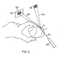
- the holographic pattern P is illuminated by a laser pen 100 of low power, for example red color of wavelength 645 nanometers.
- the distance between the laser 100 and the pattern P is not critical for image reconstruction.
- the light beam 101 from the laser 100 is diffracted by the pattern P, so that it is divided into at least two secondary beams 102 and 103 after passing through the lens 1.
- Each of the two beams 102 and 103 reconstructs an image at a distance of distance of the lens 1 which can be between 20 and 50 centimeters, for example.
- This image is revealed by placing an object 104 serving as a screen on the path of one of the two beams 102 or 103. Because the light used is from a laser, the object that serves as a screen can be any.
- the image can also be projected on an image sensor, for example of the CCD (Charge Coupled Device) or CMOS (for "Complementary Metal Oxide Semiconductor”) type to enable fast and accurate recognition.
- the images corresponding to each of the two beams 102 and 103 are referenced 105 and 106, respectively.
- the ophthalmic lens 1 may be intended to be assembled in a pair of glasses.
- the pattern P may be small and printed near an edge of the lens 1 ( figure 5 ).
- the transferred pattern P may occupy a portion of the face of the lens 1 which is less than 25 mm 2.
- the pattern can also be introduced on a part of the lens to be cut off. In this case the pattern is mainly introduced for purposes of traceability of the final product.
- Such a configuration is particularly interesting if the transferred pattern corresponds to a computer generated hologram CGH type and which consists of pixels.
- Such a hologram can thus contain a very large amount of information over a very small space, advantageously between 15 mm 2 and 0.5 mm 2 , making it possible, for example, to guarantee complete traceability of the optical article in the production line and logistics.
- the transferred pattern P can occupy the entire anterior face of the lens 1, for example when it gives the lens a particular optical function. This may be the case, in particular, when the transferred pattern P consists of a set of electrically conductive wires parallel to a given direction, for filtering light passing through the lens according to a polarization thereof.
- the conductive wires have a width of a few tens of nanometers and are spaced two by two by a few tens of nanometers.
- an intermediate layer may be deposited on the membrane 11 of the tampon before the layer of transferable material 14, to adjust a surface energy between the layer 14 and the membrane 11 of the buffer. Such an adjustment can further improve the transfer of the portions 3 of transferable material to the lens 1.
- the pattern transferred to the lens can be a diffracting pattern, that is to say whose visibility results from a diffraction of the light by the portions 3 and / or the gaps 4 present therebetween.
- the pattern that is transferred may be visible under ambient lighting conditions, or when illuminated by a laser beam.
- the key parameter of the process is the state of the Latex layer at the time of step / c /: bringing the surface of the pad into contact which comprises the layer of transferable material with the Latex layer.
- the layer of latex thus deposited retains its properties for about ten seconds, a period of time that defines the process window during which the transfer must be performed.
- the exemplified method is optimized for a digital holographic pattern composed of square elementary pixels having a dimension of 1 ⁇ m on each side.
- the membrane 11 of the tampon carries on its surface a microrelief consisting of recesses 12 and protuberances 13 of rectangular profile as schematized on the figure 1.a .
- the depth of the microrelief (altitude difference between the hollows 12b and the protuberances 13) is 1 .mu.m.
- the holographic pattern has characteristics such that the width of the protuberances of the microrelief carried by the membrane 11 and measured along an axis parallel to an edge of the square pixels varies between 1 .mu.m and 85 .mu.m depending on the area of the buffer considered.
- the metal layer is obtained by evaporation under vacuum.
- the suitable metallic material is placed in a crucible and heated by Joule effect.
- the evaporation is carried out on the Sylgard® 184 buffer which has not undergone any prior surface preparation.
- the evaporation of the metal layer takes place in the same day as the transfer step on the ophthalmic lens.
- the transfer of the layer 14 is selectively: only the portions of material initially located on the protuberances (13) of the buffer are transferred.
- the transferred holographic pattern is of amplitude hologram type.
- the protuberances of the surface of the buffer can penetrate entirely into the latex layer.
- the transfer of the layer 14 is integral: all the portions of the transferable layer 14 present on the protuberances 13 and the recesses 12b are transferred.
- the integral transfer of the portions of the layer 14 is accompanied by the permanent deposition of the latex layer, reproducing the microrelief complementary to the microrelief constituting the pattern P of the buffer.
- the transferred holographic pattern is of the phase hologram type, covered with a metal layer.
- Buffering is orthogonal to the surface.
- This limit pressure P is determined for a layer of 30 nm of gold or aluminum, on the latex deposited under the conditions described above.
- the pressure applied for stamping the tampon on the convex face of an ophthalmic lens (with a radius of curvature 120 mm) coated with a layer of latex deposited under the conditions described above is 1.5 g / mm. 2 .
- the transfer of the 30 nm gold layer is selective; the hologram obtained is an amplitude hologram.
- the pressure applied for stamping the tampon on the convex face of an ophthalmic lens (with a radius of curvature 120 mm) coated with a layer of latex deposited under the conditions described above is 1.5 g / mm. 2 .
- the transfer of the 30 nm aluminum layer is integral, and the latex layer is permanently embedded, so that the microrelief of the latex layer is the microrelief complementary to the microrelief constituting the pattern P on the surface of the buffer.
- the hologram obtained is a phase hologram.
Landscapes
- Engineering & Computer Science (AREA)
- Health & Medical Sciences (AREA)
- Ophthalmology & Optometry (AREA)
- Manufacturing & Machinery (AREA)
- Mechanical Engineering (AREA)
- Physics & Mathematics (AREA)
- General Health & Medical Sciences (AREA)
- General Physics & Mathematics (AREA)
- Optics & Photonics (AREA)
- Diffracting Gratings Or Hologram Optical Elements (AREA)
- Holo Graphy (AREA)
- Eyeglasses (AREA)
- Polarising Elements (AREA)
- Optical Fibers, Optical Fiber Cores, And Optical Fiber Bundles (AREA)
Abstract
Description
La présente invention concerne un procédé de transfert d'un motif de taille micronique sur un article optique, ainsi qu'un article optique comprenant un tel motif en utilisant ce procédé. Elle est particulièrement adaptée à un produit du type lentille optique, notamment du type lentille ophtalmique. Ce procédé est très avantageux pour introduire un motif holographique.The present invention relates to a method for transferring a micron-sized pattern to an optical article, and to an optical article comprising such a pattern using this method. It is particularly suitable for a product of the optical lens type, in particular of the ophthalmic lens type. This method is very advantageous for introducing a holographic pattern.
Il peut être nécessaire d'imprimer un motif déterminé sur un produit fini ou en cours de fabrication, notamment dans un but de décoration, pour indiquer une marque du produit ou pour empêcher d'éventuelles contrefaçons du produit, par exemple.It may be necessary to print a specific pattern on a finished product or in the process of manufacture, especially for decorative purposes, to indicate a brand of the product or to prevent possible counterfeiting of the product, for example.
Pour cela, plusieurs procédés d'impression ont été développés, qui sont désignés globalement par procédés de lithographie douce (pour «soft-lithography» en anglais), par opposition aux procédés lithographiques utilisés classiquement pour la fabrication de circuits électroniques intégrés. Alors que ces derniers sont basés sur l'irradiation et la dissolution sélectives de portions d'un masque de résine selon un motif déterminé, les procédés de lithographie douce utilisent un tampon dont la surface présente un microrelief constitué de creux et de protubérances. Ce microrelief définit le motif à reproduire sur le produit. Le motif est reproduit sur une face du produit par application du tampon, dans des conditions qui sont adaptées en fonction du matériau présent à la surface du produit.For this, several printing processes have been developed, which are generally designated by soft lithography methods (for "soft-lithography" in English), as opposed to lithographic processes conventionally used for the manufacture of integrated electronic circuits. While the latter are based on the selective irradiation and dissolution of portions of a resin mask according to a given pattern, the soft lithography processes use a buffer whose surface has a microrelief consisting of hollows and protuberances. This microrelief defines the pattern to reproduce on the product. The pattern is reproduced on one side of the product by applying the stamp, under conditions that are adapted according to the material present on the surface of the product.
On désigne par motif l'arrangement géométrique des portions de surface des protubérances mises au contact de la surface du produit lorsque le tampon est appliquéGeometric arrangement of the surface portions of the protuberances contacted with the surface of the product when the tampon is applied
Dans le procédé de lithographie douce appelé impression par micro-contact («micro-contact printing» en anglais), la face du produit est recouverte d'une couche métallique et le tampon est enduit d'une substance capable de protéger la couche métallique pendant une étape de gravure. Lors de l'application du tampon sur la face du produit, une partie de la substance est sélectivement transférée du tampon sur la couche métallique à des endroits qui correspondent aux protubérances du tampon. La couche métallique n'est ensuite gravée qu'aux endroits de celle-ci qui correspondent aux creux du tampon. Or il est nécessaire d'utiliser une substance qui forme une couche moléculaire auto-assemblée sur la couche métallique pour obtenir une qualité d'impression satisfaisante. Pour cela, la couche métallique doit être dépourvue de pollutions et être constituée d'un métal peu sujet à une éventuelle altération chimique de surface, telle qu'une oxydation. Dans la pratique, seuls l'or, le platine et l'argent permettent d'obtenir une qualité d'impression satisfaisante. Un tel choix du matériau qui constitue le motif imprimé est particulièrement réduit, et peut être incompatible avec d'autres contraintes du produit, telles que son prix de revient. En outre, un tel procédé est long à mettre en oeuvre, notamment à cause de l'étape de gravure de la couche métallique qui est généralement réalisée en utilisant une solution liquide d'un agent de gravure.In the process of soft lithography called micro-contact printing, the face of the product is covered with a metal layer and the pad is coated with a substance capable of protecting the metal layer during an etching step. When applying the pad to the product face, a portion of the substance is selectively transferred from the pad to the metal layer at locations that correspond to the protuberances of the buffer. The metal layer is then etched only at the places thereof that correspond to the hollows of the buffer. Now it is necessary to use a substance that forms a self-assembled molecular layer on the metal layer to obtain a satisfactory print quality. For this, the metal layer must be free of pollution and consist of a little metal subject to possible chemical surface alteration, such as oxidation. In practice, only gold, platinum and silver make it possible to obtain a satisfactory print quality. Such a choice of material which constitutes the printed pattern is particularly small, and may be incompatible with other constraints of the product, such as its cost price. In addition, such a method is long to implement, in particular because of the etching step of the metal layer which is generally performed using a liquid solution of an etching agent.
Le document
Le document
Un but de la présente invention est de proposer un procédé de transfert d'un motif qui est simple à mettre en oeuvre et compatible avec un grand nombre de matériaux constituant le motif. La présente invention doit notamment permettre le transfert sur un article optique d'un motif présentant une définition à l'échelle micronique, voire sub-micronique, un tel motif constituant avantageusement un hologramme.An object of the present invention is to provide a method of transferring a pattern which is simple to implement and compatible with a large number of materials constituting the pattern. The present invention must in particular allow the transfer on an optical article of a pattern having a definition at the micron scale, or even sub-micron, such a pattern advantageously constituting a hologram.
D'une façon générale au sens de l'invention, l'emploi du terme micronique englobe à la fois un motif micronique présentant une définition à l'échelle de la taille du micron, et un motif submicronique présentant une définition à l'échelle inférieure à la taille du micron soit à l'échelle de la centaine voire cinquantaine de nanomètres.In general terms within the meaning of the invention, the use of the term micron encompasses both a micron pattern presenting a definition at the micron size scale, and a submicron pattern having a lower scale definition. the size of the micron is at the scale of hundreds or even fifty nanometers.
Pour cela, l'invention propose un procédé de transfert d'un motif micronique, tel que défini précédemment, sur une surface d'un article optique qui comprend les étapes suivantes :
- /a/ déposer une couche d'au moins un matériau transférable sur une surface d'un tampon comportant des creux et des protubérances, constituant le microrelief à définition micronique ou sub-micronique, correspondant au motif à transférer ;
- /b/ déposer une couche d'un latex sous forme liquide sur la surface du substrat de l'article optique;
- /c/ avant que la couche de latex soit sèche, mettre en contact la surface du tampon qui comprend la couche de matériau transférable avec la couche de latex.
- /d/ appliquer une pression sur le tampon; et
- /e/ écarter le tampon de la surface de l'article optique comprenant la couche de latex.
- / a / depositing a layer of at least one transferable material on a surface of a buffer comprising recesses and protuberances, constituting the micro-relief with micron or sub-micron definition corresponding to the pattern to be transferred;
- / b / depositing a layer of a latex in liquid form on the surface of the substrate of the optical article;
- Before the latex layer is dry, contact the surface of the pad which comprises the layer of transferable material with the latex layer.
- / d / apply a pressure on the buffer; and
- / e / remove the pad from the surface of the optical article comprising the latex layer.
Selon l'invention la couche de matériau transférable déposée sur le microrelief du tampon lors de l'étape /a/ n'épouse généralement pas de façon conforme le microrelief. La couche est présente préférentiellement sur les zones du microrelief qui s'apparentent à des plans orthogonaux à la direction principale dans laquelle s'est effectué le dépôt de matière. Ces zones sont portées par les protubérances (13) ou les creux du tampon (12b), comme indiqué dans la
Un procédé selon l'invention est donc du type lithographie douce et, de ce fait présente des avantages spécifiques. En particulier, le procédé ne comprend aucune étape de gravure car les portions de la couche de matériau transférable qui sont initialement situées dans les creux de la surface du tampon ne sont pas mises en contact avec la couche de latex qui joue le rôle de matériau adhésif, et de ce fait ne sont pas transférées à la surface du latex. Ce procédé est précis, et présente l'avantage d'être non polluant, aucune étape de gravure chimique étant nécessaire.A method according to the invention is therefore of the soft lithography type and, as a result, has specific advantages. In particular, the method does not include any etching step because the portions of the layer of transferable material that are initially located in the depressions of the surface of the pad are not brought into contact with the latex layer which acts as an adhesive material , and thus are not transferred to the surface of the latex. This method is precise and has the advantage of being non-polluting, no chemical etching step being necessary.
Dans le procédé selon l'invention, une couche de latex encore partiellement liquide assure l'adhésion, sur la surface de l'article optique , des portions de la couche de matériau transférable qui sont transférées pendant l'application du tampon. Un tel mécanisme d'adhésion est compatible avec un grand nombre de matériaux transférables, notamment des matériaux conducteurs électriquement, des matériaux métalliques, isolants, diélectriques, ou réfringents. De plus, l'adhésion qui est ainsi obtenue est peu affectée par des pollutions présentes sur l'article optique ou sur la couche de matériau transférable.In the method according to the invention, a layer of still partially liquid latex ensures adhesion, on the surface of the optical article, portions of the layer of transferable material that are transferred during the application of the buffer. Such an adhesion mechanism is compatible with a a large number of transferable materials, including electrically conductive materials, metallic, insulating, dielectric, or refractile materials. In addition, the adhesion which is thus obtained is little affected by pollution present on the optical article or on the layer of transferable material.
Un avantage de l'invention réside dans les conditions de mise en contact du tampon revêtu d'au moins une couche de matériau transférable sur la surface de l'article optique revêtu d'au moins une couche de latex. Ces conditions concernent essentiellement les propriétés de la couche de latex, la pression d'application du tampon et sa durée. Elles peuvent être contrôlées, avec des moyens simples et peu onéreux qui sont couramment disponibles. Les conditions d'obtention d'une couche de latex aux propriétés adéquates relèvent du savoir-faire de l'homme de l'art. Parmi les conditions de mise en contact du tampon avec la surface de l'article optique, d'une façon avantageuse, le procédé selon l'invention est réalisé dans des conditions telles que le tampon présente une approche parallèle à la normale du point de contact sur le substrat de l'article optique.An advantage of the invention lies in the contacting conditions of the pad coated with at least one layer of transferable material on the surface of the optical article coated with at least one layer of latex. These conditions essentially concern the properties of the latex layer, the application pressure of the buffer and its duration. They can be controlled, with simple and inexpensive means that are commonly available. The conditions for obtaining a latex layer with adequate properties are within the skill of those skilled in the art. Among the conditions for bringing the pad into contact with the surface of the optical article, advantageously, the process according to the invention is carried out under conditions such that the buffer has an approach parallel to the normal of the point of contact. on the substrate of the optical article.
L'utilisation d'un latex dans ce type de procédé est particulièrement avantageuse dans la mesure où le latex présente une propriété adhésive qui n'existe que de façon transitoire durant la phase de séchage. Il n'est donc pas indispensable après avoir mis en oeuvre le procédé de retirer la couche de latex sur l'article optique en dehors de la zone portant le motif. Le caractère adhésif de la couche de latex disparaît à mesure qu'elle sèche et que les particules de latex coalescent.The use of a latex in this type of process is particularly advantageous insofar as the latex has an adhesive property which exists only transiently during the drying phase. It is therefore not essential after carrying out the method of removing the latex layer on the optical article outside the area carrying the pattern. The adhesive nature of the latex layer disappears as it dries and the latex particles coalesce.
D'autre part, l'utilisation d'un latex dans ce type de procédé est également très avantageuse dans la mesure òu selon un mode de réalisation de l'invention le latex est apte à reproduire un microrelief spécifique imposé par la pression d'un microrelief maître.On the other hand, the use of a latex in this type of process is also very advantageous insofar as according to one embodiment of the invention the latex is capable of reproducing a specific microrelief imposed by the pressure of a master microrelief.
Comme mentionné précédemment, le motif peut être micronique ou submicronique, le terme micronique étant utilisé d'une façon générale dans l'ensemble de la description pour désigner ces deux tailles de motifs. Ainsi d'une façon générale au sens de l'invention, on entend par motif micronique un motif comprenant un ou plusieurs motifs élémentaires; chaque motif élémentaire présentant une taille comprise entre 10 µm (micromètre) et 50 nm (nanomètre), avantageusement entre 5 µm et 100 nm, et très avantageusement entre 3 µm et 150 nm.As mentioned above, the pattern may be micron or submicron, the term micron being generally used throughout the description to refer to these two pattern sizes. Thus, in a general sense within the meaning of the invention, micronic pattern comprising one or more elementary patterns; each elementary pattern having a size between 10 .mu.m (micrometer) and 50 nm (nm), advantageously between 5 .mu.m and 100 nm, and very advantageously between 3 .mu.m and 150 nm.
Le motif transféré peut être, en particulier, un motif diffractant lorsqu'il est éclairé par un faisceau lumineux. Ce peut être notamment un motif holographique. Un tel motif est particulièrement adapté pour permettre d'identifier un produit et/ou de distinguer un produit original d'une copie de contrefaçon. Plus particulièrement, le procédé selon l'invention est particulièrement adapté pour introduire un hologramme d'amplitude sur l'article optique. On désigne par hologramme d'amplitude une microstructure holographique qui affecte préférentiellement l'amplitude du champ électromagnétique en incidence normale. C'est le cas en particulier d'un hologramme composé d'un arrangement de zones transparentes et de zones opaques, qui sont également réfléchissantes dans le cas ou l'opacité est obtenue par un métal. Une image de lecture correspondant à l'hologramme peut alors être visualisée par transmission ou par réflexion d'un faisceau lumineux sur la lentille.The transferred pattern may be, in particular, a diffracting pattern when illuminated by a light beam. This may be in particular a holographic pattern. Such a pattern is particularly suitable for identifying a product and / or distinguishing an original product from a counterfeit copy. More particularly, the method according to the invention is particularly suitable for introducing an amplitude hologram on the optical article. An amplitude hologram denotes a holographic microstructure that preferentially affects the amplitude of the electromagnetic field in normal incidence. This is the case in particular of a hologram composed of an arrangement of transparent areas and opaque areas, which are also reflective in the case where the opacity is obtained by a metal. A reading image corresponding to the hologram can then be visualized by transmission or reflection of a light beam on the lens.
Le motif transféré selon l'invention est également adapté pour introduire un hologramme de phase sur l'article optique. On désigne par hologramme de phase une microstructure holographique qui affecte préférentiellement la phase du champ électromagnétique en incidence normale.The transferred pattern according to the invention is also adapted to introduce a phase hologram on the optical article. A phase hologram denotes a holographic microstructure that preferentially affects the phase of the electromagnetic field at normal incidence.
Le motif lui-même peut aussi représenter un logo ou une inscription directement lisible sur l'article optique. Lorsque le motif est constitué d'une pluralité de motifs élémentaires et identiques, il peut être à la fois du type holographique et posséder une signification directement lisible sur l'article optique.The pattern itself may also represent a logo or directly readable inscription on the optical article. When the pattern consists of a plurality of elementary and identical patterns, it can be both holographic and have a directly readable meaning on the optical article.
Le motif holographique peut également être de type hologramme numérique, c'est-à-dire un hologramme généré par ordinateur (souvent dénommé par l'acronyme anglais « CGH » pour « Computer Generated Hologramme »). Dans un tel cas, le motif holographique peut être constitué d'un ensemble de pixels contigus, chaque pixel ayant une surface comprise entre 0,2 µm2 et 25 µm2, avantageusement entre 0,2 µm2 et 4 µm2. Préférentiellement, le motif comprendra un grand nombre de pixels, par exemple, un nombre total supérieur à 10 000 pixels, permettant ainsi d'obtenir par reconstruction sous illumination une image présentant une résolution suffisante.The holographic pattern may also be of the digital hologram type, that is, a computer-generated hologram (often referred to by the acronym "CGH" for "Computer Generated Hologram"). In such a case, the holographic pattern may be constituted a set of contiguous pixels, each pixel having a surface area of between 0.2 μm 2 and 25 μm 2 , advantageously between 0.2 μm 2 and 4 μm 2 . Preferably, the pattern will comprise a large number of pixels, for example a total number greater than 10 000 pixels, thus making it possible to obtain by reconstruction under illumination an image having a sufficient resolution.
Le motif transféré peut occuper une partie réduite d'une face de l'article, notamment pour ne pas masquer ledit article lui-même ou pour ne pas gêner une utilisation ultérieure de l'article. Dans une telle configuration, le motif occupera de façon préférentielle une partie de la face de l'article inférieure à 25 mm2.The transferred pattern may occupy a reduced portion of a face of the article, in particular to not hide said article itself or to hinder subsequent use of the article. In such a configuration, the pattern will preferentially occupy a portion of the face of the article less than 25 mm 2 .
Alternativement, le motif transféré peut occuper sensiblement toute une face de l'article, notamment lorsqu'il comprend un réseau de fils microniques ou submicroniques. Un tel motif occupant toute une face de l'article peut être réalisé pour obtenir une fonction antistatique à la surface de l'article optique, pour réaliser un ensemble d'électrodes d'une matrice d'affichage ou encore une fonction de filtrage en polarisation d'une lumière réfléchie ou transmise par l'article optique. Dans ce dernier cas, l'effet polarisant est obtenu en transférant un motif de fils conducteurs parallèles (réseau de type polariseur à fil ou « wire-grid » selon la dénomination anglaise).Alternatively, the transferred pattern can occupy substantially a whole face of the article, especially when it comprises a network of micron or submicron wires. Such a pattern occupying an entire face of the article can be made to obtain an antistatic function on the surface of the optical article, for producing a set of electrodes of a display matrix or a polarization filtering function. a light reflected or transmitted by the optical article. In the latter case, the polarizing effect is obtained by transferring a pattern of parallel conductive yarns (wire-grid or wire-grid type network).
Avantageusement, un traitement de la surface de l'article optique peut être effectué avant de disposer la couche de latex sur la surface dudit article optique. Ce traitement est notamment choisi parmi un traitement chimique, thermique, plasma et corona. Ce traitement de la surface peut notamment comprendre un traitement chimique consistant en un nettoyage avec de l'isopropanol et/ou de l'eau de la surface de l'article optique. Ainsi, des poussières ou salissures éventuellement présentes sur cette surface peuvent être retirées.Advantageously, a treatment of the surface of the optical article can be performed before disposing the latex layer on the surface of said optical article. This treatment is in particular chosen from a chemical, thermal, plasma and corona treatment. This surface treatment may in particular comprise a chemical treatment consisting of cleaning with isopropanol and / or water from the surface of the optical article. Thus, dust or dirt possibly present on this surface can be removed.
La couche de latex peut dans le cadre de l'invention être déposée par un procédé de centrifugation (spin coating), procédé bien intégré notamment dans les chaînes de production de lentilles ophtalmiques. Elle peut également être déposée par d'autres techniques de dépôt telles que le trempage (dip-coating), le spray, le jet de matière à l'aide de buses d'une tête d'impression jet d'encre. L'épaisseur de la couche de latex déposée à la surface de l'article optique est généralement comprise entre 0,2 µm et 50 µm, avantageusement entre 1 µm et 10 µm. La couche doit être optiquement transparente. Son taux de transmission peut être variable, notamment en cas de couche teintée, mais elle ne doit ni diffuser, ni diffracter, ni modifier la perception d'un objet observé par transparence au travers de l'article optique comprenant une telle couche de matériau adhésif.The latex layer may, in the context of the invention, be deposited by a spin coating process, a well-integrated process, in particular in the production lines of ophthalmic lenses. It can also be deposited by other deposition techniques such as dipping (dip-coating), the spray, the jet of material using nozzles of an inkjet print head. The thickness of the latex layer deposited on the surface of the optical article is generally between 0.2 μm and 50 μm, advantageously between 1 μm and 10 μm. The layer must be optically transparent. Its transmission rate may be variable, especially in the case of a tinted layer, but it must neither diffuse nor diffract or modify the perception of an object observed by transparency through the optical article comprising such a layer of adhesive material .
Le procédé peut comprendre en outre l'étape suivante, qui est réalisée après l'étape /a/ et/ou l'étape /e/:
- /f/ recouvrir la surface de l'article optique par un ou plusieurs revêtements fonctionnalisés.
- / f / covering the surface of the optical article with one or more functionalized coatings.
Ces revêtements fonctionnalisés peuvent être déposés sous forme de film ou de vernis monocouche ou multicouches, par tout moyen de dépôt tel que par exemple le trempage, la centrifugation, le spray, ou l'impression par jet de matière par les buses d'une tête d'impression jet d'encre. Ils sont avantageusement choisis parmi les revêtements présentant une fonctionnalité de type anti-choc, anti-abrasion, antireflet, antisalissure, antibuée, antistatique, polarisante, colorante et photochromique.These functionalized coatings can be deposited in the form of a film or a monolayer or multilayer varnish, by any deposition means such as, for example, dipping, centrifuging, spraying, or jet printing of material by the nozzles of a head. inkjet printing. They are advantageously chosen from coatings having a type of anti-shock, anti-abrasion, anti-reflective, anti-fouling, anti-fog, antistatic, polarizing, coloring and photochromic function.
Selon un mode préférentiel de l'invention, le procédé comprend ainsi une étape supplémentaire qui est réalisée après l'étape /e/ et qui consiste à recouvrir la surface de l'article optique par au moins un revêtement fonctionnalisé par dessus le motif transféré et la couche de latex. Ce revêtement en plus de sa fonctionnalisation constitue avantageusement un revêtement de protection du motif transféré.According to a preferred embodiment of the invention, the method thus comprises an additional step which is performed after step / e / and which consists in covering the surface of the optical article with at least one functionalized coating over the transferred pattern and the latex layer. This coating in addition to its functionalization advantageously constitutes a protective coating of the transferred pattern.
Le matériau transférable peut être un matériau métallique tel que, par exemple, de l'or, de l'aluminium, du chrome, de l'argent, du cuivre, du nickel, du platine, du palladium ou un alliage comprenant l'un au moins de ces métaux. Dans ce cas, la couche de matériau transférable peut être avantageusement déposée à l'étape /a/ sur la surface du tampon par évaporation sous vide ou par pulvérisation cathodique sous vide (sputtering). D'une façon générale, on a pu constater que plus le temps entre le dépôt de la couche métallique sur le tampon et la réalisation de l'étape /c/ est court, meilleur est le transfert de ladite couche métallique sur le latex. Ceci s'explique notamment par une absence de contamination de la couche métallique qui pénalise la qualité de l'adhésion.The transferable material may be a metallic material such as, for example, gold, aluminum, chromium, silver, copper, nickel, platinum, palladium or an alloy comprising one at least of these metals. In this case, the layer of transferable material may advantageously be deposited in step / a / on the surface of the buffer by vacuum evaporation or by sputtering. In general, it has been found that the longer the time between the deposition of the metal layer on the pad and the realization of step / c / is short, best is the transfer of said metal layer on the latex. This is explained in particular by an absence of contamination of the metal layer which penalizes the quality of adhesion.
Alternativement, la couche de matériau transférable peut comprendre un empilement de plusieurs couches de matériaux respectifs. Le matériau de l'une au moins des couches de l'empilement peut alors être réfringent. Dans ce cas, la visualisation du motif transféré peut aussi résulter partiellement d'un comportement interférentiel d'un faisceau lumineux utilisé pour éclairer le motif. Le transfert d'un empilement de plusieurs couches matériaux peut ainsi conduire, en fonction de l'épaisseur dudit empilement, à la réalisation d'un hologramme qui affecte très notablement la phase du champ électromagnétique en incidence normale Un tel transfert permet ainsi de se rapprocher des conditions de réalisation d'un hologramme de phase. On désigne par hologramme de phase une microstructure holographique qui affecte préférentiellement la phase du champ électromagnétique en incidence normale.Alternatively, the layer of transferable material may comprise a stack of several layers of respective materials. The material of at least one of the layers of the stack can then be refractive. In this case, the visualization of the transferred pattern may also result partially from an interferential behavior of a light beam used to illuminate the pattern. The transfer of a stack of several material layers can thus lead, depending on the thickness of said stack, to the realization of a hologram that very significantly affects the phase of the electromagnetic field in normal incidence. Such a transfer thus makes it possible to approach conditions for producing a phase hologram. A phase hologram denotes a holographic microstructure that preferentially affects the phase of the electromagnetic field at normal incidence.
Selon un premier mode de mise en oeuvre de l'invention, la surface du tampon est appliquée contre la surface de l'article optique qui porte la couche de latex, à l'étape /c/, dans des conditions adaptées de sorte que les portions de la couche de matériau transférable qui sont situées sur les protubérances de la surface du tampon sont sélectivement transférées sur la surface de l'article optique. Selon ce premier mode, les portions de la couche de matériau transférable qui se situent dans les creux du tampon ne sont pas transférées sur la surface de l'article optique lors de l'application du tampon car les creux du microrelief ne sont pas mis en contact avec la couche de latex. Pour cela, le tampon est appliqué à l'étape /c/ avec une pression modérée, de sorte que les protubérances du tampon ne pénètrent pas dans la couche de latex. La couche de latex conserve alors une épaisseur sensiblement constante sur la face de l'article optique, au moins dans la partie de cette face qui est occupée par le motif transféré. Le contraste du motif transféré résulte alors de la présence ou de l'absence de matériau transférable sur la surface de l'article, en des endroits différents du motif. Dans ce cas, le motif transféré forme une juxtaposition de zones opaques et transparentes, et si ce motif forme une structure diffractive holographique, le résultat est un hologramme d'amplitude. Dans ce mode de réalisation de l'invention, la combinaison du transfert sélectif, du matériau transférable présent sur les protubérances, sur l'article optique, et l'absence de pénétration du latex dans les creux du motif, permettent la formation d'un hologramme d'amplitude.According to a first embodiment of the invention, the surface of the buffer is applied against the surface of the optical article which carries the latex layer, in step / c /, under suitable conditions so that the portions of the layer of transferable material that are located on the protuberances of the surface of the pad are selectively transferred to the surface of the optical article. According to this first mode, the portions of the layer of transferable material that are in the hollows of the buffer are not transferred to the surface of the optical article during the application of the buffer because the hollows of the microrelief are not set. contact with the latex layer. For this, the buffer is applied at step / c / with a moderate pressure, so that the protuberances of the buffer do not penetrate into the latex layer. The latex layer then retains a substantially constant thickness on the face of the optical article, at least in the portion of that face that is occupied by the transferred pattern. The contrast of the transferred pattern then results from the presence or absence of transferable material on the surface of the article at different locations of the pattern. In this case, the transferred pattern forms a juxtaposition of opaque and transparent areas, and if this pattern forms a diffractive structure holographic, the result is an amplitude hologram. In this embodiment of the invention, the combination of the selective transfer, the transferable material present on the protuberances, the optical article, and the absence of penetration of the latex into the hollows of the pattern, allow the formation of a amplitude hologram.
Selon un second mode de mise en oeuvre de l'invention, la surface du tampon est appliquée contre la surface de l'article optique qui porte la couche de latex, à l'étape /c/, dans des conditions adaptées de sorte que les protubérances de la surface du tampon pénètrent complètement dans la couche de latex de sorte que les portions de la couche de matériau transférable qui sont situées sur les protubérances de la surface du tampon ainsi que celles situées dans les creux du tampon sont conjointement transférées sur la surface de l'article optique. De préférence, la surface du tampon est appliquée pendant une durée adaptée, c'est-à-dire un temps de séchage adapté, de sorte qu'après éloignement du tampon la couche de latex présente des enfoncements permanents créés par la pénétration des protubérances du tampon dans la couche de latex. La couche de latex présente ainsi à sa surface un microrelief qui n'est autre que le complémentaire du microrelief porté par la surface du tampon. Autrement dit, le motif est moulé dans la couche de latex. Le microrelief porté par la couche de latex est constitué de creux et de protubérances. Les creux et les protubérances sont recouverts de portions de la couche métallique transférées. Dans ce cas, le contraste du motif transféré peut résulter, au moins en partie, des variations d'épaisseur de la couche de latex. Lorsque le motif transféré est un motif holographique, le microrelief obtenu peut constituer un hologramme de phase. On désigne par hologramme de phase une microstructure holographique qui affecte préférentiellement la phase du champ électromagnétique en incidence normale.According to a second embodiment of the invention, the surface of the buffer is applied against the surface of the optical article which carries the latex layer, in step / c /, under suitable conditions so that the protuberances of the pad surface penetrate completely into the latex layer so that the portions of the layer of transferable material that are located on the protuberances of the pad surface as well as those in the pad recesses are co-transferred to the surface of the optical article. Preferably, the surface of the pad is applied for a suitable duration, that is to say a suitable drying time, so that after removal of the buffer the latex layer has permanent depressions created by the penetration of the protuberances of the buffer in the latex layer. The latex layer thus has on its surface a microrelief which is none other than the complement of the microrelief carried by the surface of the pad. In other words, the pattern is molded into the latex layer. The microrelief carried by the latex layer consists of recesses and protuberances. The depressions and protuberances are covered with portions of the metal layer transferred. In this case, the contrast of the transferred pattern may result, at least in part, from thickness variations of the latex layer. When the transferred pattern is a holographic pattern, the resulting microrelief may constitute a phase hologram. A phase hologram denotes a holographic microstructure that preferentially affects the phase of the electromagnetic field at normal incidence.
L'invention propose aussi un article optique qui comprend un motif transféré sur une surface de celui-ci en utilisant un procédé tel que décrit précédemment. Cet article optique comprend une lentille optique d'instrumentation, une lentille optique de visée, une visière, ainsi qu'une lentille ophtalmique, et en particulier une telle lentille qui est adaptée pour être assemblée dans une monture de paire de lunettes. Une telle lentille comprend alors elle-même :
- une lentille de base comprenant au moins un substrat organique ou minéral,
- une couche de latex séché, et
- des portions d'un matériau transférable formant le motif transféré, par adhésion sur la lentille de base via la couche de latex.
- a base lens comprising at least one organic or inorganic substrate,
- a layer of dried latex, and
- portions of transferable material forming the transferred pattern by adhesion to the base lens via the latex layer.
La lentille de base comprend notamment un substrat organique. Par substrat, on entend le matériau transparent constitutif de base de la lentille optique et plus particulièrement de la lentille ophtalmique. Ce matériau sert de support à l'empilement d'un ou plusieurs revêtements, et participe à créer la fonction correctrice de la lentille dans le cas d'une lentille ophtalmique correctrice. Dans le cas où l'article optique est une lentille ophtalmique sont adaptés, par exemple, les substrats du type polycarbonates; polyamides ; polyimides ; polysulfones ; copolymères de polyéthylènetérephtalate et polycarbonate; polyoléfines, notamment polynorbornènes ; polymères et copolymères de diéthylène glycol bis(allylcarbonate); polymères et copolymères (méth)acryliques notamment polymères et copolymères (méth)acryliques dérivés de bisphenol-A; polymères et copolymères thio(méth)acryliques ; polymères et copolymères uréthane et thiouréthane ; polymères et copolymères époxy et polymères et copolymères épisulfide. Dans certains cas, les substrat peuvent être teintés directement dans la masse.The base lens comprises in particular an organic substrate. By substrate is meant the basic constituent transparent material of the optical lens and more particularly of the ophthalmic lens. This material serves as a support for the stacking of one or more coatings, and helps to create the corrective function of the lens in the case of a corrective ophthalmic lens. In the case where the optical article is an ophthalmic lens are suitable, for example, substrates of the polycarbonate type; polyamides; polyimides; polysulfones; copolymers of polyethylene terephthalate and polycarbonate; polyolefins, especially polynorbornenes; polymers and copolymers of diethylene glycol bis (allyl carbonate); (meth) acrylic polymers and copolymers, especially polymers and (meth) acrylic copolymers derived from bisphenol-A; thio (meth) acrylic polymers and copolymers; urethane and thiourethane polymers and copolymers; epoxy polymers and copolymers and episulfide polymers and copolymers. In some cases, the substrates can be tinted directly in the mass.
Entre le substrat organique et la couche de latex, un ou plusieurs revêtements peuvent optionnellement être présents. Ces revêtements sont notamment les revêtements fonctionnalisés tels que décrits précédemment.Between the organic substrate and the latex layer, one or more coatings may optionally be present. These coatings include functionalized coatings as described above.
Etant donné que la lentille est essentiellement transparente, lorsque le motif est de type holographique, il peut être adapté pour former une image de lecture lorsqu'un faisceau lumineux est envoyé à travers la lentille à l'endroit du motif.Since the lens is substantially transparent, when the pattern is of the holographic type, it can be adapted to form a read image when a light beam is sent through the lens at the location of the pattern.
La couche de latex peut former en outre une protection de la lentille contre des chocs éventuels reçus ultérieurement par celle-ci. Avantageusement, une couche d'un matériau résistant à des rayures est aussi formée sur la lentille, par dessus la couche de latex et le motif transféré.The latex layer may further form a protection of the lens against any shocks subsequently received by it. Advantageously, a layer of a scratch-resistant material is also formed on the lens, over the latex layer and the transferred pattern.
D'autres particularités et avantages de la présente invention apparaîtront dans la description ci-après de deux exemples de mise en oeuvre non limitatifs, en référence aux dessins annexés, dans lesquels :
- les
figures 1 a et 1 b sont des vues en coupe d'un tampon utilisé dans un procédé de transfert selon l'invention ; - les
figures 2a et 2b illustrent des étapes ultérieures du procédé ; - les
figures 3 et 4 sont des vues en coupe de motifs transférés selon deux modes de mise en oeuvre de l'invention ; et - la
figure 5 illustre une étape de lecture d'un motif holographique transféré selon l'invention.
- the
figures 1 a and 1b are sectional views of a buffer used in a transfer process according to the invention; - the
Figures 2a and 2b illustrate subsequent steps of the process; - the
Figures 3 and 4 are sectional views of patterns transferred according to two embodiments of the invention; and - the
figure 5 illustrates a step of reading a transferred holographic pattern according to the invention.
Pour raison de clarté, les dimensions des différents éléments représentés sur ces figures ne sont pas en proportion avec des dimensions ou des rapports de dimensions réels. Par ailleurs, sur toutes les figures, des références identiques correspondent à des éléments identiques.For the sake of clarity, the dimensions of the various elements shown in these figures are not in proportion to dimensions or ratios of real dimensions. Moreover, in all the figures, identical references correspond to identical elements.
On décrit maintenant l'invention dans le cadre du transfert d'un motif holographique sur une lentille ophtalmique. Dans cette description, des étapes élémentaires du procédé de l'invention qui sont connues individuellement de procédés existants ne sont pas reprises en détail. On s'attache seulement à décrire une succession d'étapes élémentaires qui permet de réaliser un transfert selon l'invention.The invention is now described in connection with the transfer of a holographic pattern onto an ophthalmic lens. In this description, elementary steps of the process of the invention which are known individually from existing processes are not repeated in detail. It is only necessary to describe a succession of elementary steps that makes it possible to perform a transfer according to the invention.
Conformément à la
Avantageusement, une couche facilitant la désolidarisation de la couche métallique 14 d'avec la membrane 11 peut être déposée sur la surface S avant le dépôt de la couche de matériau transférable 14.Advantageously, a layer facilitating the separation of the
La surface S peut se déformer lors d'une application de celle-ci contre la surface réceptrice, en fonction d'une courbure de cette dernière. Cette déformation peut résulter d'un écrasement de la membrane qui varie le long de la surface S, et/ou d'un recul variable de la membrane lorsqu'elle est fixée d'une façon appropriée sur la base 10.The surface S can be deformed during an application thereof against the receiving surface, depending on a curvature of the latter. This deformation can result from a crushing of the membrane which varies along the surface S, and / or from a variable recoil of the membrane when it is suitably fixed on the
La
Conformément à la
La lentille ophtalmique 1 peut être d'un type quelconque tel que décrit précédemment. Par lentille ophtalmique, on entend les Tentilles s'adaptant notamment à une monture de lunette et dont la fonction est de protéger l'oeil et/ou corriger la vue.The
Préférentiellement, la surface de la lentille 1 qui est destinée à recevoir le motif P est d'abord nettoyée. Pour cela, la lentille peut être soumise à un traitement corona ou à un traitement par plasma, mais un procédé de nettoyage au moyen d'une ou de plusieurs solutions détergentes et/ou de rinçage peut aussi être utilisé.Preferably, the surface of the
Une couche de latex sous forme liquide est formée sur la face antérieure de la lentille 1. D'une façon préférée, la couche de latex est déposée par centrifugation («spin coating» en anglais) en utilisant une solution liquide du latex, référencée 20. La lentille 1 est placée horizontalement sur un support 30 et mise en rotation autour d'un axe vertical. Le liquide 20 est alors dispensé sur la lentille 1. La vitesse de rotation de la lentille lors de l'étalement du latex détermine, d'une façon connue en soi, l'épaisseur de la couche de latex qui est formée sur la lentille. La durée de l'étalement influence le séchage de la couche de latex. La couche de latex est référencée 2 dans la suite.A latex layer in liquid form is formed on the anterior face of the
Grâce à l'utilisation d'un matériau de type latex, la face antérieure de la lentille 1 qui est recouverte par la couche 2 présente un pouvoir adhésif temporaire, tant que la couche 2 n'est pas définitivement sèche. Ce pouvoir adhésif résulte de nombreuses liaisons chimiques pendantes présentes dans le latex liquide. Plusieurs latex peuvent être utilisés pour constituer la couche 2, parmi lesquels on peut citer, à titre d'exemples, les latex de polyuréthanes, les latex de poly(meth)acrylate, les latex de polyester, les latex comprenant des unités butadiènes tels que les polybutadiènes ou les poly(styrène-butadiène). De tels latex sont notamment décrits dans les brevets
La surface S du tampon, et plus spécifiquement les protubérances 13 et les creux 12b qui portent la couche métallique 14, est alors appliquée contre la face antérieure de la lentille 1 recouverte par la couche 2. Pour cela, le tampon est approché selon une direction sensiblement perpendiculaire à la face de la lentille (
Selon un premier mode de mise en oeuvre de l'invention illustré par la
Selon un second mode de mise en oeuvre illustré par la
Une fois que la couche de latex 2 a complètement séché, elle a perdu son comportement adhésif, de sorte que la lentille 1 peut être touchée sans adhérence sur toute sa face antérieure. Simultanément, la couche 2 assure définitivement la fixation des portions 3 de matériau transférable (provenant des zones 13), ou de toutes les portions de la couche 14 transférées provenant des protubérances 13 et des creux 12b qui constitue(nt) le motif transféré P.Once the
De façon particulièrement avantageuse, la couche de latex 2 constitue en outre une protection de la lentille 1 contre des chocs. En effet, une couche de latex peut amortir un choc appliqué sur une surface. La couche 2 peut donc présenter une double fonction dans le cadre de l'invention : outre la fixation de portions de matériau transférable sur la lentille, elle protège celle-ci contre des chocs éventuels.Particularly advantageously, the
Une couche supérieure 5 peut en outre être appliquée sur la face antérieure de la lentille 1. Cette couche 5 recouvre notamment le motif transféré P. Elle peut être formée à partir d'une solution de précurseurs déposée sur la couche de latex 2 et sur les portions 3 de matériau transféré qui forment le motif P (
Dans le cas où le motif transféré constitue une structure diffractive holographique, une image de lecture diffractée par l'hologramme et restituant l'information qu'il contient peut alors être visualisée par transmission ou par réflexion d'un faisceau lumineux cohérent sur la lentille 1, à l'endroit du motif transféré P. Pour cela, conformément à la
La lentille ophtalmique 1 peut être destinée à être assemblée dans une monture de paire de lunettes. Afin de ne pas gêner la vision d'un porteur de lunettes, le motif P peut être de petites dimensions et imprimé à proximité d'un bord de la lentille 1 (
Alternativement, le motif transféré P peut occuper toute la face antérieure de la lentille 1, par exemple lorsqu'il confère à la lentille une fonction optique particulière. Ce peut être le cas, notamment, lorsque le motif transféré P est constitué d'un ensemble de fils conducteurs électriquement et parallèles à une direction déterminée, pour filtrer de la lumière qui traverse la lentille en fonction d'une polarisation de celle-ci. Typiquement, les fils conducteurs ont une largeur de quelques dizaines de nanomètres et sont espacés deux à deux de quelques dizaines de nanomètres.Alternatively, the transferred pattern P can occupy the entire anterior face of the
De nombreuses modifications du procédé de transfert qui a été décrit en détail ci-dessus peuvent être introduites, tout en conservant certains au moins des avantages de l'invention. Par exemple, une couche intermédiaire peut être déposée sur la membrane 11 du tampon avant la couche de matériau transférable 14, pour ajuster une énergie de surface entre la couche 14 et la membrane 11 du tampon. Un tel ajustement peut encore améliorer le transfert des portions 3 de matériau transférable sur la lentille 1. Par ailleurs, le motif transféré sur la lentille peut être un motif diffractant, c'est-à-dire dont la visibilité résulte d'une diffraction de la lumière par les portions 3 et/ou les intervalles 4 présents entre celles-ci. Enfin, le motif qui est transféré peut être visible dans des conditions d'éclairement ambiant, ou lorsqu'il est éclairé par un faisceau laser.Many modifications of the transfer process which have been described in detail above can be introduced while retaining at least some of the advantages of the invention. For example, an intermediate layer may be deposited on the
Le paramètre clé du procédé est l'état de la couche de Latex au moment de l'étape /c/ : mise en contact de la surface du tampon qui comprend la couche de matériau transférable avec la couche de Latex.The key parameter of the process is the state of the Latex layer at the time of step / c /: bringing the surface of the pad into contact which comprises the layer of transferable material with the Latex layer.
Lors de cette étape, la couche de Latex doit être non sèche, de façon à ce qu'elle soit :
- adhésive, pour permettre le transfert de la couche adhésive
- déformable, pour permettre au latex de se déformer définitivement, de façon à reconstituer un microrelief constitué de creux et de protubérances ; microrelief complémentaire du microrelief constituant le motif P sur la surface du tampon
- adhesive, to allow the transfer of the adhesive layer
- deformable, to allow the latex to be permanently deformed, so as to reconstitute a microrelief constituted by hollows and protuberances; complementary microrelief of the microrelief constituting the pattern P on the surface of the buffer
Nous dénommerons latex A une solution aqueuse de latex polyuréthane W234 de la société Baxenden présentant les propriétés suivantes mesurées à 21,6°C et 44% d'humidité relative :
- Viscosité : 7 centipoise
- Extrait sec : 22.25%
- Viscosity: 7 centipoise
- Dry extract: 22.25%
Une couche de latex A d'épaisseur 1 µm est déposée par centrifugation sur la face convexe d'une lentille ophtalmique à base d'Orma® (Essilor), de rayon de courbure 120 mm, selon les conditions suivantes :
- Conditions de dépôt pour l'obtention d'une couche non sèche (à 21,6°C et 44% d'humidité relative):
- dispense
de 2,5mL de Latex sur la lentille - rotation de la lentille à 2000 tours par minute durant 15 secondes
- rotation de la lentille à 2500 tours
par minute durant 2 secondes
- dispense
- Deposit conditions for obtaining a dry layer (at 21.6 ° C and 44% relative humidity):
- 2.5mL of latex on the lens
- rotation of the lens at 2000 rpm for 15 seconds
- rotation of the lens at 2500 rpm for 2 seconds
La couche de latex ainsi déposée conserve ses propriétés durant une dizaine de secondes, laps de temps qui définit la fenêtre de procédé durant laquelle le transfert doit être effectué.The layer of latex thus deposited retains its properties for about ten seconds, a period of time that defines the process window during which the transfer must be performed.
Le procédé cité en exemple est optimisé pour un motif holographique numérique composé de pixels élémentaires carrés de dimension 1 µm de côté.The exemplified method is optimized for a digital holographic pattern composed of square elementary pixels having a dimension of 1 μm on each side.
Pour ce faire, la membrane 11 du tampon porte en sa surface un microrelief consistant en des creux 12 et des protubérances 13 de profil rectangulaire comme schématisé sur la
Le motif holographique a des caractéristiques telles que la largeur des protubérances du microrelief porté par la membrane 11 et mesurée selon un axe parallèle à un bord des pixels carrés varie entre 1µm et 85µm selon la zone du tampon considérée.The holographic pattern has characteristics such that the width of the protuberances of the microrelief carried by the
Le motif à transférer est moulé dans du Sylgard® 184 (11) (Dow Coming). Les propriétés de ce matériau après polymérisation à 100°C durant 1 heure sont les suivantes:
- énergie de surface : 22 mN/m
- Module d'Young : 2,5 MPa.
- surface energy: 22 mN / m
- Young's modulus: 2.5 MPa.
La couche métallique est obtenue par évaporation sous vide. Le matériau métallique adéquat est disposé dans un creuset, et chauffé par effet Joule. L'évaporation est effectuée sur le tampon en Sylgard® 184 n'ayant subi aucune préparation de surface préalable.The metal layer is obtained by evaporation under vacuum. The suitable metallic material is placed in a crucible and heated by Joule effect. The evaporation is carried out on the Sylgard® 184 buffer which has not undergone any prior surface preparation.
Dans le cas de l'or ; une couche de 30 nm d'épaisseur est obtenue en évaporant de l'or d'une pureté de 99.9%.In the case of gold; a
Dans le cas de l'aluminium ; une couche de 30 nm d'épaisseur est obtenue en évaporant des grenailles d'aluminium d'une pureté de 99.5%.In the case of aluminum; a
L'évaporation de la couche métallique a lieu dans la même journée que l'étape de transfert sur la lentille ophtalmique.The evaporation of the metal layer takes place in the same day as the transfer step on the ophthalmic lens.
Dans le cas du premier mode de mise en oeuvre de l'invention : le transfert de la couche 14 se fait sélectivement : seules les portions de matériau initialement situées sur les protubérances (13) du tampon sont transférées. Le motif holographique transféré est de type hologramme d'amplitude.In the case of the first mode of implementation of the invention: the transfer of the
Dans cas du second mode de mise en oeuvre de l'invention : les protubérances de la surface du tampon peuvent pénétrer entièrement dans la couche de latex. Le transfert de la couche 14 est intégral : toutes les portions de la couche transférable 14 présentes sur les protubérances 13 et les creux 12b sont transférées. Le transfert intégral des portions de la couche 14 s'accompagne de l'enfoncement permanent de la couche de latex, reproduisant le microrelief complémentaire du microrelief constituant le motif P du tampon. Le motif holographique transféré est de type hologramme de phase, recouvert d'une couche métallique.In the case of the second mode of implementation of the invention: the protuberances of the surface of the buffer can penetrate entirely into the latex layer. The transfer of the
Le tamponnage se fait orthogonalement à la surface.Buffering is orthogonal to the surface.
De la pression de tamponnage appliquée dépend le résultat du transfert, et donc le mode de mise en oeuvre de l'invention :
- Si cette pression est inférieure à une pression Plimite : le transfert est sélectif ; il s'agit du premier mode de mise en oeuvre de l'invention : hologramme d'amplitude.
- If this pressure is lower than a limit pressure P: the transfer is selective; it is the first mode of implementation of the invention: amplitude hologram.
Si cette pression est supérieure à une pression Plimite : le transfert est intégral, et s'accompagne de l'enfoncement permanent de la couche de Latex, reproduisant le microrelief complémentaire du microrelief constituant le motif P sur le tampon.If this pressure is greater than a limit pressure P: the transfer is complete, and is accompanied by the permanent deposition of the Latex layer, reproducing the microrelief complementary to the microrelief constituting the pattern P on the pad.
Cette pression Plimite est déterminée pour une couche de 30 nm d'or ou d'aluminium, sur le latex déposé dans les conditions décrites ci-dessus.This limit pressure P is determined for a layer of 30 nm of gold or aluminum, on the latex deposited under the conditions described above.
Elle est de Plimite = 45 à 60 g/mm2 de la surface des protubérances 13 du tampon constituant le motif P.It is P limit = 45 to 60 g / mm 2 of the surface of the
Le tableau ci-après présente les résultats de différentes conditions testées:
La pression appliquée pour le tamponnage du tampon sur la face convexe d'une lentille ophtalmique (d'un rayon de courbure 120 mm) recouverte d'une couche de latex déposée dans les conditions décrites ci-dessus est de 1,5 g/mm2. Le transfert de la couche d'or de 30nm est sélectif ; l'hologramme obtenu est un hologramme d'amplitude.The pressure applied for stamping the tampon on the convex face of an ophthalmic lens (with a radius of curvature 120 mm) coated with a layer of latex deposited under the conditions described above is 1.5 g / mm. 2 . The transfer of the 30 nm gold layer is selective; the hologram obtained is an amplitude hologram.
Pressions appliquées pour l'exemple du transfert intégral d'aluminium. avec enfoncement permanent de la couche de latex A, reproduisant à l'inverse les creux 12 et les protubérances 13 du tampon, constituant le motif P : Pressures applied for the example of the complete transfer of aluminum. with permanent deposition of the latex layer A, reproducing the
La pression appliquée pour le tamponnage du tampon sur la face convexe d'une lentille ophtalmique (d'un rayon de courbure 120 mm) recouverte d'une couche de latex déposée dans les conditions décrites ci-dessus est de 1,5 g/mm2. Le transfert de la couche d'aluminium de 30 nm est intégral, et la couche de latex est enfoncée définitivement, de façon que le microrelief de la couche de latex soit le microrelief complémentaire du microrelief constituant le motif P sur la surface du tampon. L'hologramme obtenu est un hologramme de phase.The pressure applied for stamping the tampon on the convex face of an ophthalmic lens (with a radius of curvature 120 mm) coated with a layer of latex deposited under the conditions described above is 1.5 g / mm. 2 . The transfer of the 30 nm aluminum layer is integral, and the latex layer is permanently embedded, so that the microrelief of the latex layer is the microrelief complementary to the microrelief constituting the pattern P on the surface of the buffer. The hologram obtained is a phase hologram.
Claims (38)
- A method of transferring a micron-scale pattern (P) onto a surface of an optical article (1), the method comprising the following steps:a) depositing a layer of at least one transferable material on a surface of a stamp having recesses (12) and protuberances (13) constituting a micro-relief with micron-scale or submicron-scale definition, corresponding to the pattern to be transferred;b) depositing a layer of a latex in the liquid form on the surface of the substrate of the optical article;c) before the layer of latex is dry, bringing the surface of the stamp that includes the layer of transferable material into contact with the layer of latex;d) applying a pressure to the stamp; ande) removing the stamp from the surface of the optical article comprising the layer of latex.
- Method according to claim 1, in which the micron-scale pattern comprises one or more individual patterns, each individual pattern having a dimension in the range 10 µm to 50 nm, advantageously in the range 5 µm to 100 nm, and highly advantageously in the range 3 µm to 150 nm.
- Method according to claim 1 or claim 2, in which the recesses (12) and the protuberances (13)have dimensions in the range 10 micrometers to 50 nanometers, measured parallel to the membrane (11).
- Method according to any one of the preceding claims, in which the depth of the recesses is in the range 0.1 µm to 30 µm, advantageously in the range 0.1 µm to 10 µm.
- Method according to any one of the preceding claims, in which the transferred pattern (P) is a diffracting pattern when said pattern is illuminated by a beam of light.
- Method according to any one of the preceding claims, in which the transferred pattern (P) is a holographic pattern.
- Method according to claim 6, in which the transferred pattern (P) is an amplitude hologram type holographic pattern.
- Method according to claim 6, in which the transferred pattern (P) is a phase hologram type holographic pattern.
- Method according to claim 6, in which the transferred pattern is a digital hologram type holographic pattern constituted by a set of contiguous pixels, each pixel having a surface area in the range 0.2 µm2 to 25 µm2, advantageously in the range 0.2 µm2 to 4 µm2.
- Method according to any one of the preceding claims, in which the transferred pattern (P) occupies a small portion of a face of the optical article (1).
- Method according to claim 10, in which the transferred pattern (P) occupies a portion of the face of the optical article (1) of less than 25 mm2.
- Method according to any one of claims 1 to 8, in which the transferred pattern (P) occupies an entire face of the optical article (1).
- Method according to claim 12, in which the transferred pattern (P) comprises an array of parallel electrically conductive wires.
- Method according to any one of claims 1 to 11, in which the holographic pattern (P) is adapted to form a reading image when a beam of light (101) is passed through the lens (1) at the location of said pattern.
- Method according to claim 1, in which the layer of latex (2) is deposited on the surface of the optical article (1) using a spin-coating method.
- Method according to claim 15, in which the thickness of the layer of latex is in the range 0.2 µm to 50 µm, preferably in the range 1 µm to 10 µm.
- Method according to claim 7, in which in step c) the surface (S) of the stamp is applied against the surface of the optical article (1) carrying the layer of latex (2) under conditions such that the layer of transferable material (14) located on the protuberances (13) of the surface of the stamp is selectively transferred onto the surface of said article.
- Method according to claim 17, in which in step c) the surface (S) of the stamp is applied against the surface of the optical article (1) carrying the layer of latex (2) with pressure in the range 0.1 g/mm2 to 60 g/mm2 of surface of the protuberances of pattern P.
- Method according to claim 8, in which in step c) the surface (S) of the stamp is applied against the surface of the optical article (1) carrying the layer of latex (2) under conditions such that the protuberances (13) of the surface of the stamp penetrate completely into the layer of latex, and such that the portions of the layer of transferable material that are located on the protuberances (13) of the surface of the stamp as well as those located in the recesses (12b) of the stamp are jointly transferred onto the surface of said optical article.
- Method according to claim 19, in which in step c) the surface (S) of the stamp is applied against the surface of the optical article (1) carrying the layer of latex (2) at a pressure of more than 60 g/mm2 of the surface of the protuberances of pattern P.
- Method according to claim 1, further comprising the following step, carried out after step a) and/or step e):f) covering the surface of the optical article with one or more functionalized coatings.
- Method according to claim 21, in which the functionalized coating has an anti-shock, anti-abrasion, antireflective, soil-repellent, anti-fogging, antistatic, polarizing, coloring, or photochromic function.
- Method according to claim 21 or claim 22, in which the additional step f) is carried out after step e).
- Method according to claim 1, in which the transferable material is a metallic material.
- Method according to claim 24, in which the transferable material is selected from gold, aluminum, chromium, silver, copper, nickel, platinum, palladium, and an alloy comprising at least one of said metals.
- Method according to claim 24 or claim 25, in which the layer of transferable material is deposited in step a) onto the surface (S) of the stamp by vacuum evaporation or vacuum cathodic sputtering.
- Method according to any one of claims 24 to 26, in which the layer of transferable material (14) comprises a stack of a plurality of layers of respective materials.
- Method according to claim 27, in which the material of at least one of the layers of the stack is refringent.
- Method according to claim 1, in which the stamp is based on polydimethylsiloxane at least at the location of the protuberances (13) of the surface (S) of the stamp.
- Method according to claim 1, in which the stamp is approached parallel to the normal at the point of contact on the substrate of the optical article.
- Method according to any one of the preceding claims, in which in step c) the surface (S) of the stamp is adapted to deform during application against the surface of the product (1) as a function of a curvature of said product surface.
- Method according to any one of the preceding claims, further comprising a step of processing the surface of the optical article (1) carried out before step b).
- Method according to claim 1, in which the optical article (1) is selected from an instrumentation optical lens, a viewing lens, a visor, and an ophthalmic lens.
- Method according to claim 33, in which the optical article (1) is an ophthalmic lens selected from afocal, single vision, bifocal, trifocal, and progressive power lenses.
- An optical article (1) representing an ophthalmic lens, said lens itself comprising:a base lens comprising at least one organic or mineral substrate;a layer of dried latex (2); andportions of a transferable material forming a transferred pattern (P),the pattern being transferred on a surface of the base lens using a method according to any one of the preceding claims, by adhesion to the base lens via the layer of dried latex.
- Article according to claim 35, in which the pattern (P) is formed by several portions of printing material located at the same level on the layer of latex (2) in a direction perpendicular to said layer and separated by gaps (4a) that are free of transferred material.
- Article according to claim 35, in which the pattern (P) is embossed into the layer of latex (2) and in which several portions of transferred material (3, 4b) are located at different engraving depths into the layer of latex.
- Article according to any one of the claims 35 to 37, in which the layer of latex (2) further forms a protection for the lens (1) against shocks which may subsequently be received by said lens.
Priority Applications (1)
| Application Number | Priority Date | Filing Date | Title |
|---|---|---|---|
| PL06841872T PL1957274T3 (en) | 2005-12-08 | 2006-12-06 | Method for transferring a micron pattern on an optical pattern and the thus obtained optical pattern |
Applications Claiming Priority (2)
| Application Number | Priority Date | Filing Date | Title |
|---|---|---|---|
| FR0512492A FR2894515B1 (en) | 2005-12-08 | 2005-12-08 | METHOD OF TRANSFERRING A MICRONIC PATTERN TO AN OPTICAL ARTICLE AND OPTICAL ARTICLE THUS OBTAINED |
| PCT/FR2006/002665 WO2007066006A2 (en) | 2005-12-08 | 2006-12-06 | Method for transferring a micron pattern on an optical pattern and the thus obtained optical pattern |
Publications (2)
| Publication Number | Publication Date |
|---|---|
| EP1957274A2 EP1957274A2 (en) | 2008-08-20 |
| EP1957274B1 true EP1957274B1 (en) | 2010-03-24 |
Family
ID=36928296
Family Applications (1)
| Application Number | Title | Priority Date | Filing Date |
|---|---|---|---|
| EP06841872A Active EP1957274B1 (en) | 2005-12-08 | 2006-12-06 | Method for transferring a micron pattern on an optical pattern and the thus obtained optical pattern |
Country Status (14)
| Country | Link |
|---|---|
| US (1) | US7874671B2 (en) |
| EP (1) | EP1957274B1 (en) |
| JP (1) | JP5424645B2 (en) |
| KR (1) | KR101370552B1 (en) |
| CN (1) | CN101326058B (en) |
| AT (1) | ATE461815T1 (en) |
| AU (1) | AU2006323921B2 (en) |
| BR (1) | BRPI0619528A8 (en) |
| CA (1) | CA2632525C (en) |
| DE (1) | DE602006013186D1 (en) |
| FR (1) | FR2894515B1 (en) |
| PL (1) | PL1957274T3 (en) |
| PT (1) | PT1957274E (en) |
| WO (1) | WO2007066006A2 (en) |
Families Citing this family (20)
| Publication number | Priority date | Publication date | Assignee | Title |
|---|---|---|---|---|
| FR2879313B1 (en) * | 2004-12-10 | 2007-04-06 | Essilor Int | METHOD OF RECORDING DATA ON A LENS, AND LENS COMPRISING DATA RECORDED |
| JP5214232B2 (en) * | 2007-12-20 | 2013-06-19 | Asti株式会社 | Plastic microstructure manufacturing method |
| JP2010287625A (en) * | 2009-06-09 | 2010-12-24 | Toshiba Corp | Template and pattern forming method |
| CN102653190A (en) * | 2011-03-04 | 2012-09-05 | 国家纳米科学中心 | Method for forming graphene oxide pattern and graphene pattern |
| JP2012242582A (en) * | 2011-05-19 | 2012-12-10 | Sakusan:Kk | Spectacle lens |
| CN102350853B (en) * | 2011-07-19 | 2013-11-20 | 陈炜玲 | Production technique of holographic pattern film, holographic pattern film and system |
| EP2604415B1 (en) * | 2011-12-15 | 2017-05-24 | Essilor International (Compagnie Générale D'Optique) | System and method for generating machine marking instructions |
| TWM429700U (en) * | 2012-01-19 | 2012-05-21 | Benq Materials Corp | Engraving device |
| CN104903112B (en) * | 2012-12-31 | 2017-12-26 | 3M创新有限公司 | The micro-contact printing with high relief pressing mold in volume to volume processing |
| KR20200128762A (en) * | 2014-02-06 | 2020-11-16 | 비전 이즈, 엘피 | Wire grid polarizer and method of manufacture |
| DE102015109703B4 (en) * | 2015-06-17 | 2022-03-17 | tooz technologies GmbH | Spectacle lens, spectacles and method for producing a spectacle lens |
| KR20160039588A (en) * | 2016-03-22 | 2016-04-11 | 주식회사 우리옵토 | Micro-pattern formaing method on optical lenz having a certain curvature |
| CN106273218A (en) * | 2016-06-15 | 2017-01-04 | 东莞科大光学镜片有限公司 | The manufacture method of a kind of fog-proof lens and goods thereof |
| EP3812142A1 (en) * | 2019-10-23 | 2021-04-28 | Carl Zeiss Vision International GmbH | Method for producing a spectacle lens and a product comprising a spectacle lens |
| EP3988290A1 (en) | 2020-10-23 | 2022-04-27 | Carl Zeiss Vision International GmbH | Method for manufacturing a spectacle lens |
| EP3988288A1 (en) | 2020-10-23 | 2022-04-27 | Carl Zeiss Vision International GmbH | Method of manufacturing a spectacle lens |
| EP3988289A1 (en) | 2020-10-23 | 2022-04-27 | Carl Zeiss Vision International GmbH | Method of manufacturing a spectacle lens |
| CN113427888B (en) * | 2021-06-15 | 2022-06-17 | 清华大学 | Seal unit design method, seal unit and seal |
| CN114516188A (en) * | 2022-02-17 | 2022-05-20 | 深圳睿晟自动化技术有限公司 | Hot pressing process for micro-nano level optical waveguide mirror |
| WO2023175193A2 (en) * | 2022-03-18 | 2023-09-21 | Carl Zeiss Vision International Gmbh | Coated lens and method for manufacturing the same |
Family Cites Families (44)
| Publication number | Priority date | Publication date | Assignee | Title |
|---|---|---|---|---|
| DE2613034A1 (en) | 1976-03-26 | 1977-09-29 | Siemens Ag | FALSE-PROOF IDENTITY CARD WITH LIPPMANN-BRAGG HOLOGRAM |
| FR2507196A1 (en) * | 1981-06-09 | 1982-12-10 | Euverte Bernard | Adhesive transfer sheets carrying discontinuous coatings - esp. for transfer to wide surfaces |
| JPH0614414B2 (en) * | 1986-06-17 | 1994-02-23 | 共同印刷株式会社 | Transfer type optical recording medium |
| JP2899296B2 (en) * | 1988-11-10 | 1999-06-02 | アレン・エル・コーエン | Manufacturing method of multifocal phase plate |
| JPH04147180A (en) | 1990-10-09 | 1992-05-20 | Dainippon Printing Co Ltd | Patterned computer hologram |
| US5634669A (en) | 1991-04-16 | 1997-06-03 | American Bank Note Holographics, Inc. | Holographic check authentication article |
| JPH0749471A (en) * | 1993-08-06 | 1995-02-21 | Kuraray Co Ltd | Spectacles |
| DE69428901T2 (en) | 1993-08-06 | 2002-06-27 | Commonwealth Scientific And Industrial Research Organisation, Campbell | DIFFERENTIAL DEVICE |
| CA2173855C (en) | 1993-10-29 | 2007-06-26 | Mieczyslaw H. Mazurek | Pressure-sensitive adhesives having microstructured surfaces |
| US5752442A (en) * | 1993-11-03 | 1998-05-19 | Corning Incorporated | Method for printing a color filter |
| JP3552262B2 (en) * | 1994-02-09 | 2004-08-11 | 凸版印刷株式会社 | Hologram seal and method of manufacturing the same |
| JPH07261010A (en) * | 1994-03-18 | 1995-10-13 | Shimadzu Corp | Replica diffraction grating |
| JP3372258B2 (en) * | 1995-08-04 | 2003-01-27 | インターナシヨナル・ビジネス・マシーンズ・コーポレーシヨン | Stamps for lithography processes |
| US20080217813A1 (en) * | 1995-11-15 | 2008-09-11 | Chou Stephen Y | Release surfaces, particularly for use in nanoimprint lithography |
| US6309580B1 (en) * | 1995-11-15 | 2001-10-30 | Regents Of The University Of Minnesota | Release surfaces, particularly for use in nanoimprint lithography |
| US5772905A (en) * | 1995-11-15 | 1998-06-30 | Regents Of The University Of Minnesota | Nanoimprint lithography |
| DE19644620A1 (en) | 1996-10-18 | 1998-04-23 | Chromatron Laser Sys Gmbh | Coated or deposited carrier material device |
| US5892600A (en) | 1996-12-27 | 1999-04-06 | Kuo; Wei-Wu Alex | Spectacle lens structure with a planar reflective outer surface |
| JPH1172606A (en) * | 1997-08-29 | 1999-03-16 | Shimadzu Corp | Pattern etching method for sic |
| US5937758A (en) * | 1997-11-26 | 1999-08-17 | Motorola, Inc. | Micro-contact printing stamp |
| US6060256A (en) * | 1997-12-16 | 2000-05-09 | Kimberly-Clark Worldwide, Inc. | Optical diffraction biosensor |
| DE19758395C2 (en) | 1997-12-23 | 2002-01-03 | Marcel Rogalla | Method and viewing device for holographic visualization of virtual images and patterns |
| JP2002513067A (en) * | 1998-04-24 | 2002-05-08 | ミネソタ マイニング アンド マニュファクチャリング カンパニー | Stripe adhesive coated tape |
| GB2343864B (en) | 1998-11-20 | 2003-07-16 | Agra Vadeko Inc | Improved security thread and method and apparatus for applying same to a substrate |
| US6579673B2 (en) * | 1998-12-17 | 2003-06-17 | Kimberly-Clark Worldwide, Inc. | Patterned deposition of antibody binding protein for optical diffraction-based biosensors |
| KR100307449B1 (en) * | 1999-01-13 | 2001-12-28 | 김순택 | Functional film used for cathode ray tube |
| DE19926698A1 (en) | 1999-06-11 | 2000-12-14 | Hsm Gmbh | Computer generated security feature for application to document or banknote, uses computer-generated hologram algorithm to calculate interference pattern applied to carrier |
| US6452699B1 (en) | 1999-09-28 | 2002-09-17 | Holospex, Inc. | Controlled diffraction efficiency far field viewing devices |
| JP4548679B2 (en) | 1999-10-08 | 2010-09-22 | 大日本印刷株式会社 | Adhesive for pressure-sensitive adhesive layer in volume hologram laminate |
| JP2001121582A (en) | 1999-10-26 | 2001-05-08 | Ntt Advanced Technology Corp | Mold and manufacturing method |
| WO2001044397A1 (en) * | 1999-12-15 | 2001-06-21 | Henkel Kommanditgesellschaft Auf Aktien | Transfer adhesive tape |
| US6399295B1 (en) * | 1999-12-17 | 2002-06-04 | Kimberly-Clark Worldwide, Inc. | Use of wicking agent to eliminate wash steps for optical diffraction-based biosensors |
| JP4453945B2 (en) * | 2000-09-18 | 2010-04-21 | 大日本印刷株式会社 | Transfer foil sheet and method for evaluating its peelability and breakability |
| DE10127980C1 (en) | 2001-06-08 | 2003-01-16 | Ovd Kinegram Ag Zug | Diffractive security element |
| US20030080472A1 (en) * | 2001-10-29 | 2003-05-01 | Chou Stephen Y. | Lithographic method with bonded release layer for molding small patterns |
| US7220452B2 (en) | 2001-10-31 | 2007-05-22 | Massachusetts Institute Of Technology | Multilayer transfer patterning using polymer-on-polymer stamping |
| US20030152693A1 (en) * | 2002-02-12 | 2003-08-14 | Su Kai C. | Methods of applying a coating to an optical surface |
| ATE413442T1 (en) | 2002-05-28 | 2008-11-15 | 3M Innovative Properties Co | HARDENABLE ADHESIVE OBJECTS WITH TOPOGRAPHIC FEATURES |
| US20040115279A1 (en) * | 2002-09-06 | 2004-06-17 | The Ohio State University | Microfabrication of polymer microparticles |
| US7179396B2 (en) * | 2003-03-25 | 2007-02-20 | Molecular Imprints, Inc. | Positive tone bi-layer imprint lithography method |
| JP4147180B2 (en) | 2003-12-24 | 2008-09-10 | ポーラ化成工業株式会社 | Gel-like skin external preparation |
| JP2006152074A (en) * | 2004-11-26 | 2006-06-15 | Hitachi Chem Co Ltd | Photosetting resin composition and diffraction type light condensing film using the same |
| FR2894514B1 (en) * | 2005-12-08 | 2008-02-15 | Essilor Int | METHOD OF TRANSFERRING A MICRONIC PATTERN TO AN OPTICAL ARTICLE AND OPTICAL ARTICLE THUS OBTAINED |
| ATE549294T1 (en) * | 2005-12-09 | 2012-03-15 | Obducat Ab | DEVICE AND METHOD FOR TRANSFER OF PATTERN WITH INTERMEDIATE STAMP |
-
2005
- 2005-12-08 FR FR0512492A patent/FR2894515B1/en not_active Expired - Fee Related
-
2006
- 2006-12-06 US US12/095,966 patent/US7874671B2/en active Active
- 2006-12-06 CA CA2632525A patent/CA2632525C/en not_active Expired - Fee Related
- 2006-12-06 WO PCT/FR2006/002665 patent/WO2007066006A2/en active Application Filing
- 2006-12-06 AT AT06841872T patent/ATE461815T1/en not_active IP Right Cessation
- 2006-12-06 AU AU2006323921A patent/AU2006323921B2/en not_active Ceased
- 2006-12-06 KR KR1020087016576A patent/KR101370552B1/en active IP Right Grant
- 2006-12-06 PL PL06841872T patent/PL1957274T3/en unknown
- 2006-12-06 JP JP2008543866A patent/JP5424645B2/en not_active Expired - Fee Related
- 2006-12-06 PT PT06841872T patent/PT1957274E/en unknown
- 2006-12-06 DE DE602006013186T patent/DE602006013186D1/en active Active
- 2006-12-06 CN CN2006800462292A patent/CN101326058B/en active Active
- 2006-12-06 BR BRPI0619528A patent/BRPI0619528A8/en not_active IP Right Cessation
- 2006-12-06 EP EP06841872A patent/EP1957274B1/en active Active
Also Published As
| Publication number | Publication date |
|---|---|
| KR20080080360A (en) | 2008-09-03 |
| CN101326058B (en) | 2011-05-25 |
| AU2006323921A1 (en) | 2007-06-14 |
| US7874671B2 (en) | 2011-01-25 |
| ATE461815T1 (en) | 2010-04-15 |
| PL1957274T3 (en) | 2010-08-31 |
| FR2894515A1 (en) | 2007-06-15 |
| BRPI0619528A2 (en) | 2011-10-04 |
| CA2632525A1 (en) | 2007-06-14 |
| KR101370552B1 (en) | 2014-03-06 |
| PT1957274E (en) | 2010-06-25 |
| JP5424645B2 (en) | 2014-02-26 |
| CA2632525C (en) | 2014-09-16 |
| DE602006013186D1 (en) | 2010-05-06 |
| WO2007066006A2 (en) | 2007-06-14 |
| FR2894515B1 (en) | 2008-02-15 |
| EP1957274A2 (en) | 2008-08-20 |
| CN101326058A (en) | 2008-12-17 |
| AU2006323921B2 (en) | 2012-05-24 |
| US20080316558A1 (en) | 2008-12-25 |
| WO2007066006A3 (en) | 2007-07-26 |
| BRPI0619528A8 (en) | 2018-08-14 |
| JP2009518674A (en) | 2009-05-07 |
Similar Documents
| Publication | Publication Date | Title |
|---|---|---|
| EP1957274B1 (en) | Method for transferring a micron pattern on an optical pattern and the thus obtained optical pattern | |
| EP1957275B1 (en) | Method for transferring a micron pattern on an optical pattern and the thus obtained optical pattern | |
| EP1904884B1 (en) | Pixellized transparent optical component, comprising an absorbent coating, method for making same and use in an optical element | |
| CA2568421C (en) | Method for producing a transparent optical element, an optical component involved into said method and the thus obtained optical element | |
| EP1820068B1 (en) | Method for recording data in a holographic form on a lens and a corresponding lens | |
| FR2907922A1 (en) | Smart glasses series fabricating method for use in e.g. pair of spectacles, involves depositing functional material on portion of film, cutting portion in to film sheet, and assembling portion with corresponding glass substrate | |
| EP1825319A1 (en) | Method for making a transparent optical element, optical component used in said method and resulting optical element | |
| CH713843B1 (en) | Micro-optical device with integrated focusing element and picture element structure. | |
| JP2009518674A5 (en) | ||
| CA2779101A1 (en) | Security element comprising a substrate bearing an optical structure and a reference pattern, and associated method | |
| EP1904883A1 (en) | Pixellized optical component with apodized walls, method for making same and use thereof in making a transparent optical element | |
| EP3037897A1 (en) | Method for manufacturing a display dial for portable object such as a timepiece and display dial | |
| WO2022096833A1 (en) | Method for producing a security document | |
| FR3111843A1 (en) | Methods of manufacturing optical security components, optical security components and secure objects equipped with such components | |
| BRPI0619528B1 (en) | PROCESS FOR TRANSFER OF A MICRONIC REASON ON AN OPTICAL ARTICLE AND SO OPTICAL ARTICLE OBTAINED |
Legal Events
| Date | Code | Title | Description |
|---|---|---|---|
| PUAI | Public reference made under article 153(3) epc to a published international application that has entered the european phase |
Free format text: ORIGINAL CODE: 0009012 |
|
| 17P | Request for examination filed |
Effective date: 20080523 |
|
| AK | Designated contracting states |
Kind code of ref document: A2 Designated state(s): AT BE BG CH CY CZ DE DK EE ES FI FR GB GR HU IE IS IT LI LT LU LV MC NL PL PT RO SE SI SK TR |
|
| 17Q | First examination report despatched |
Effective date: 20090525 |
|
| GRAP | Despatch of communication of intention to grant a patent |
Free format text: ORIGINAL CODE: EPIDOSNIGR1 |
|
| GRAS | Grant fee paid |
Free format text: ORIGINAL CODE: EPIDOSNIGR3 |
|
| GRAA | (expected) grant |
Free format text: ORIGINAL CODE: 0009210 |
|
| AK | Designated contracting states |
Kind code of ref document: B1 Designated state(s): AT BE BG CH CY CZ DE DK EE ES FI FR GB GR HU IE IS IT LI LT LU LV MC NL PL PT RO SE SI SK TR |
|
| REG | Reference to a national code |
Ref country code: GB Ref legal event code: FG4D Free format text: NOT ENGLISH |
|
| REG | Reference to a national code |
Ref country code: CH Ref legal event code: EP |
|
| REG | Reference to a national code |
Ref country code: IE Ref legal event code: FG4D |
|
| REF | Corresponds to: |
Ref document number: 602006013186 Country of ref document: DE Date of ref document: 20100506 Kind code of ref document: P |
|
| REG | Reference to a national code |
Ref country code: CH Ref legal event code: NV Representative=s name: ISLER & PEDRAZZINI AG |
|
| REG | Reference to a national code |
Ref country code: PT Ref legal event code: SC4A Free format text: AVAILABILITY OF NATIONAL TRANSLATION Effective date: 20100618 |
|
| REG | Reference to a national code |
Ref country code: NL Ref legal event code: VDEP Effective date: 20100324 |
|
| PG25 | Lapsed in a contracting state [announced via postgrant information from national office to epo] |
Ref country code: LT Free format text: LAPSE BECAUSE OF FAILURE TO SUBMIT A TRANSLATION OF THE DESCRIPTION OR TO PAY THE FEE WITHIN THE PRESCRIBED TIME-LIMIT Effective date: 20100324 |
|
| LTIE | Lt: invalidation of european patent or patent extension |
Effective date: 20100324 |
|
| PG25 | Lapsed in a contracting state [announced via postgrant information from national office to epo] |
Ref country code: SI Free format text: LAPSE BECAUSE OF FAILURE TO SUBMIT A TRANSLATION OF THE DESCRIPTION OR TO PAY THE FEE WITHIN THE PRESCRIBED TIME-LIMIT Effective date: 20100324 Ref country code: FI Free format text: LAPSE BECAUSE OF FAILURE TO SUBMIT A TRANSLATION OF THE DESCRIPTION OR TO PAY THE FEE WITHIN THE PRESCRIBED TIME-LIMIT Effective date: 20100324 Ref country code: LV Free format text: LAPSE BECAUSE OF FAILURE TO SUBMIT A TRANSLATION OF THE DESCRIPTION OR TO PAY THE FEE WITHIN THE PRESCRIBED TIME-LIMIT Effective date: 20100324 Ref country code: AT Free format text: LAPSE BECAUSE OF FAILURE TO SUBMIT A TRANSLATION OF THE DESCRIPTION OR TO PAY THE FEE WITHIN THE PRESCRIBED TIME-LIMIT Effective date: 20100324 |
|
| REG | Reference to a national code |
Ref country code: PL Ref legal event code: T3 |
|
| REG | Reference to a national code |
Ref country code: IE Ref legal event code: FD4D |
|
| PG25 | Lapsed in a contracting state [announced via postgrant information from national office to epo] |
Ref country code: ES Free format text: LAPSE BECAUSE OF FAILURE TO SUBMIT A TRANSLATION OF THE DESCRIPTION OR TO PAY THE FEE WITHIN THE PRESCRIBED TIME-LIMIT Effective date: 20100705 Ref country code: GR Free format text: LAPSE BECAUSE OF FAILURE TO SUBMIT A TRANSLATION OF THE DESCRIPTION OR TO PAY THE FEE WITHIN THE PRESCRIBED TIME-LIMIT Effective date: 20100625 Ref country code: NL Free format text: LAPSE BECAUSE OF FAILURE TO SUBMIT A TRANSLATION OF THE DESCRIPTION OR TO PAY THE FEE WITHIN THE PRESCRIBED TIME-LIMIT Effective date: 20100324 Ref country code: RO Free format text: LAPSE BECAUSE OF FAILURE TO SUBMIT A TRANSLATION OF THE DESCRIPTION OR TO PAY THE FEE WITHIN THE PRESCRIBED TIME-LIMIT Effective date: 20100324 Ref country code: SE Free format text: LAPSE BECAUSE OF FAILURE TO SUBMIT A TRANSLATION OF THE DESCRIPTION OR TO PAY THE FEE WITHIN THE PRESCRIBED TIME-LIMIT Effective date: 20100324 Ref country code: EE Free format text: LAPSE BECAUSE OF FAILURE TO SUBMIT A TRANSLATION OF THE DESCRIPTION OR TO PAY THE FEE WITHIN THE PRESCRIBED TIME-LIMIT Effective date: 20100324 |
|
| PG25 | Lapsed in a contracting state [announced via postgrant information from national office to epo] |
Ref country code: BG Free format text: LAPSE BECAUSE OF FAILURE TO SUBMIT A TRANSLATION OF THE DESCRIPTION OR TO PAY THE FEE WITHIN THE PRESCRIBED TIME-LIMIT Effective date: 20100624 Ref country code: CZ Free format text: LAPSE BECAUSE OF FAILURE TO SUBMIT A TRANSLATION OF THE DESCRIPTION OR TO PAY THE FEE WITHIN THE PRESCRIBED TIME-LIMIT Effective date: 20100324 Ref country code: IS Free format text: LAPSE BECAUSE OF FAILURE TO SUBMIT A TRANSLATION OF THE DESCRIPTION OR TO PAY THE FEE WITHIN THE PRESCRIBED TIME-LIMIT Effective date: 20100724 Ref country code: SK Free format text: LAPSE BECAUSE OF FAILURE TO SUBMIT A TRANSLATION OF THE DESCRIPTION OR TO PAY THE FEE WITHIN THE PRESCRIBED TIME-LIMIT Effective date: 20100324 |
|
| PLBE | No opposition filed within time limit |
Free format text: ORIGINAL CODE: 0009261 |
|
| STAA | Information on the status of an ep patent application or granted ep patent |
Free format text: STATUS: NO OPPOSITION FILED WITHIN TIME LIMIT |
|
| PG25 | Lapsed in a contracting state [announced via postgrant information from national office to epo] |
Ref country code: DK Free format text: LAPSE BECAUSE OF FAILURE TO SUBMIT A TRANSLATION OF THE DESCRIPTION OR TO PAY THE FEE WITHIN THE PRESCRIBED TIME-LIMIT Effective date: 20100324 Ref country code: IE Free format text: LAPSE BECAUSE OF FAILURE TO SUBMIT A TRANSLATION OF THE DESCRIPTION OR TO PAY THE FEE WITHIN THE PRESCRIBED TIME-LIMIT Effective date: 20100324 |
|
| 26N | No opposition filed |
Effective date: 20101228 |
|
| PG25 | Lapsed in a contracting state [announced via postgrant information from national office to epo] |
Ref country code: IT Free format text: LAPSE BECAUSE OF FAILURE TO SUBMIT A TRANSLATION OF THE DESCRIPTION OR TO PAY THE FEE WITHIN THE PRESCRIBED TIME-LIMIT Effective date: 20100324 |
|
| BERE | Be: lapsed |
Owner name: ESSILOR INTERNATIONAL (COMPAGNIE GENERALE D'OPTIQ Effective date: 20101231 |
|
| PG25 | Lapsed in a contracting state [announced via postgrant information from national office to epo] |
Ref country code: MC Free format text: LAPSE BECAUSE OF NON-PAYMENT OF DUE FEES Effective date: 20101231 |
|
| PG25 | Lapsed in a contracting state [announced via postgrant information from national office to epo] |
Ref country code: BE Free format text: LAPSE BECAUSE OF NON-PAYMENT OF DUE FEES Effective date: 20101231 |
|
| PG25 | Lapsed in a contracting state [announced via postgrant information from national office to epo] |
Ref country code: CY Free format text: LAPSE BECAUSE OF FAILURE TO SUBMIT A TRANSLATION OF THE DESCRIPTION OR TO PAY THE FEE WITHIN THE PRESCRIBED TIME-LIMIT Effective date: 20100324 |
|
| PG25 | Lapsed in a contracting state [announced via postgrant information from national office to epo] |
Ref country code: HU Free format text: LAPSE BECAUSE OF FAILURE TO SUBMIT A TRANSLATION OF THE DESCRIPTION OR TO PAY THE FEE WITHIN THE PRESCRIBED TIME-LIMIT Effective date: 20100925 Ref country code: LU Free format text: LAPSE BECAUSE OF NON-PAYMENT OF DUE FEES Effective date: 20101206 |
|
| PG25 | Lapsed in a contracting state [announced via postgrant information from national office to epo] |
Ref country code: TR Free format text: LAPSE BECAUSE OF FAILURE TO SUBMIT A TRANSLATION OF THE DESCRIPTION OR TO PAY THE FEE WITHIN THE PRESCRIBED TIME-LIMIT Effective date: 20100324 |
|
| REG | Reference to a national code |
Ref country code: FR Ref legal event code: PLFP Year of fee payment: 10 |
|
| PGFP | Annual fee paid to national office [announced via postgrant information from national office to epo] |
Ref country code: CH Payment date: 20151228 Year of fee payment: 10 |
|
| PGFP | Annual fee paid to national office [announced via postgrant information from national office to epo] |
Ref country code: PT Payment date: 20151120 Year of fee payment: 10 Ref country code: PL Payment date: 20151119 Year of fee payment: 10 |
|
| REG | Reference to a national code |
Ref country code: FR Ref legal event code: PLFP Year of fee payment: 11 |
|
| REG | Reference to a national code |
Ref country code: CH Ref legal event code: PL |
|
| PG25 | Lapsed in a contracting state [announced via postgrant information from national office to epo] |
Ref country code: PT Free format text: LAPSE BECAUSE OF NON-PAYMENT OF DUE FEES Effective date: 20170606 |
|
| PG25 | Lapsed in a contracting state [announced via postgrant information from national office to epo] |
Ref country code: CH Free format text: LAPSE BECAUSE OF NON-PAYMENT OF DUE FEES Effective date: 20161231 Ref country code: LI Free format text: LAPSE BECAUSE OF NON-PAYMENT OF DUE FEES Effective date: 20161231 |
|
| REG | Reference to a national code |
Ref country code: FR Ref legal event code: PLFP Year of fee payment: 12 |
|
| REG | Reference to a national code |
Ref country code: DE Ref legal event code: R081 Ref document number: 602006013186 Country of ref document: DE Owner name: ESSILOR INTERNATIONAL, FR Free format text: FORMER OWNER: ESSILOR INTERNATIONAL (COMPAGNIE GENERALE D'OPTIQUE), CHARENTON-LE-PONT, FR |
|
| PG25 | Lapsed in a contracting state [announced via postgrant information from national office to epo] |
Ref country code: PL Free format text: LAPSE BECAUSE OF NON-PAYMENT OF DUE FEES Effective date: 20161206 |
|
| REG | Reference to a national code |
Ref country code: GB Ref legal event code: 732E Free format text: REGISTERED BETWEEN 20180517 AND 20180523 |
|
| REG | Reference to a national code |
Ref country code: FR Ref legal event code: TP Owner name: ESSILOR INTERNATIONAL, FR Effective date: 20180601 |
|
| P01 | Opt-out of the competence of the unified patent court (upc) registered |
Effective date: 20230525 |
|
| PGFP | Annual fee paid to national office [announced via postgrant information from national office to epo] |
Ref country code: GB Payment date: 20231227 Year of fee payment: 18 |
|
| PGFP | Annual fee paid to national office [announced via postgrant information from national office to epo] |
Ref country code: FR Payment date: 20231227 Year of fee payment: 18 |
|
| PGFP | Annual fee paid to national office [announced via postgrant information from national office to epo] |
Ref country code: DE Payment date: 20231229 Year of fee payment: 18 |