EP1954104A1 - Interface for switch signals and digital signals with protective circuit - Google Patents
Interface for switch signals and digital signals with protective circuit Download PDFInfo
- Publication number
- EP1954104A1 EP1954104A1 EP07122645A EP07122645A EP1954104A1 EP 1954104 A1 EP1954104 A1 EP 1954104A1 EP 07122645 A EP07122645 A EP 07122645A EP 07122645 A EP07122645 A EP 07122645A EP 1954104 A1 EP1954104 A1 EP 1954104A1
- Authority
- EP
- European Patent Office
- Prior art keywords
- interface
- signals
- network
- circuit
- signal
- Prior art date
- Legal status (The legal status is an assumption and is not a legal conclusion. Google has not performed a legal analysis and makes no representation as to the accuracy of the status listed.)
- Granted
Links
Images


Classifications
-
- H—ELECTRICITY
- H05—ELECTRIC TECHNIQUES NOT OTHERWISE PROVIDED FOR
- H05B—ELECTRIC HEATING; ELECTRIC LIGHT SOURCES NOT OTHERWISE PROVIDED FOR; CIRCUIT ARRANGEMENTS FOR ELECTRIC LIGHT SOURCES, IN GENERAL
- H05B47/00—Circuit arrangements for operating light sources in general, i.e. where the type of light source is not relevant
- H05B47/10—Controlling the light source
- H05B47/175—Controlling the light source by remote control
- H05B47/18—Controlling the light source by remote control via data-bus transmission
Definitions
- the application relates to an interface that can be supplied as permissible signals on the one hand digital signals and on the other hand signals from a button or switch to the same input-side terminals. Both signal types are passed on the output side of the interface such that logical states can be passed to a control unit according to the logic state of the respective input-side signal. Since both types of signal are permitted, for example, the concern of a mains voltage level in the case of a push-button or switch control must lead neither to destruction nor to a shutdown of the interface.
- the interface also has a receiving branch for digital signals, which are transmitted to the input-side terminals of the interface to the connected bus lines.
- the output signals of the interface can, as I said, be passed to a control unit, which is part of a building services equipment, for example.
- a control unit which is part of a building services equipment, for example.
- building technology devices may include, for example, actuators, sensors or operating devices for lighting.
- the invention relates in particular to the control of dimmable operating devices for lighting, in which a dimming can be triggered both by digital signals and by push-button or switch signals.
- the invention has set itself the task of achieving a safe execution of such an interface with relatively few electronic components. This object is achieved by the features of the independent claims.
- the dependent claims further form the central idea of the invention in a particularly advantageous manner.
- a first aspect of the invention relates to an interface for operating devices for lighting.
- the interface has a first connection, to which signals or digital signals originating either from a mains-powered pushbutton or switch can be applied, a signal processing circuit which processes the respectively applied signals and at a second connection for transmission to a control unit of a connected operating device provides for controlling the lighting means according to the respective applied signal.
- a protection circuit is provided which prevents damage to the interface at the input-side concern of a mains voltage signal. In the normal state, the protection circuit sets the signal processing circuit in a state in which it is configured for the preparation of push-button or switch signals.
- the protection circuit Only when the protection circuit does not detect a presence of a mains voltage signal at the first terminal for a predetermined period of time does it place the signal processing circuit in a state where the latter is configured to process digital signals.
- the predetermined period of time can be at least as long as a half-wave of the mains voltage.
- the protection circuit which may be an integrated circuit, for example, can immediately configure the interface for line voltage signals when it is on Concerns a mains voltage signal detected.
- a current limiting resistor may be connected, which is bypassed by the protective circuit for configuring the interface for digital signals by closing a circuit breaker.
- the switch is designed such that the shutdown of the mains voltage takes place in any case faster than the mains voltage can rise above a defined reference voltage level.
- the current limiting resistor for safety against a permanent concern of the mains voltage at the input terminals of the interface is so high-impedance dimensioned that it can absorb such a fault.
- a constant current source may be connected in parallel, which is connected in series with the circuit breaker to generate a defined current flow at the input-side concern of the digital signals.
- the circuit breaker may e.g. a transistor which is optionally designed together with the protection circuit as an integrated circuit.
- the two optocouplers (2, 3) and the rectifier can be integrated into a circuit.
- the entire interface circuit can be incorporated as an integrated circuit in a standard IC package, which is very space-saving. This is especially advantageous for a LED control gear.
- the interface can furthermore have a reception branch for digital signals, which can be connected to the first connection, which can be supplied to the interface of the control unit of a connected operating device.
- the interface may include a potential separation unit (e.g., an optocoupler) connected on the primary side to the first terminal and on the secondary side to the second terminal.
- a potential separation unit e.g., an optocoupler
- the protection circuit may further comprise a microcontroller whose function will be explained in detail below.
- the invention also relates to a system having an interface of the type described above and an operating device for lighting or other controllable building services equipment.
- the operating device may be e.g. to act a ballast for gas discharge lamps or LEDs.
- the invention also relates to a method for operating an interface for operating devices for controlling lighting means, wherein the interface has a first terminal, to which either from a supplied with mains power button or switch originating signals or digital signals can be applied, a signal processing circuit , which processes the respectively applied signals and provides them at a second connection for transmission to a control unit of a connected operating device for controlling the lighting means in accordance with the respective applied signal.
- the signal processing circuit In the normal state, the signal processing circuit is set in a state in which it is configured for the preparation of push-button or switch signals. Only if for a predetermined period of time at the first port no concern a Mains voltage signal is detected, the signal processing circuit is placed in a state in which it is configured for conditioning of digital signals.
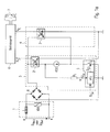
- Fig. 1a an interface is shown, at whose input side terminals KK 'a signal level can be applied.
- the applied signal can either be a digital bus voltage signal U bus with DC voltage levels in an amplitude range of up to 30 V, as is the case with the industry standards DALI and DSI.
- a signal from a button or switch is applied.
- this button or switch for providing an AC mains voltage U can be designed network with a peak voltage level of 220 V, for example, so that potentially, depending on the push button or switch operation, this AC mains voltage U network can be applied to the terminals KK '.
- the information is coded on the button or switch signals continuous time over the duration of the respective preferably manual operation.
- Push-button or switch signals are therefore of significantly lower frequency compared to digital signals.
- Digital signals are encoded via high-frequency switching operations.
- the interface can be separate from the operating device 6 or else integrated in the same housing or even on the same board.
- the interface does not require its own separate power supply. However, a voltage supply can be done via the input-side connections, since the quiescent level (logic "zero") is selected at the DALI standard not equal to 0 volts.
- the transmission branch is in Fig. 1a denoted by the reference numeral 5.
- a reception branch can also be provided (in Fig. 1a designated by the reference numeral 4).
- the interface is supplied with control signals at a connection K E by the operating device 6, and the interface then outputs digital signals conditioned on the respective standard at the external connections KK '.
- the present invention also protects this optional receiving branch against a mains voltage U Netz applied to the terminals KK ' .
- a filter and overvoltage protection circuit 1 which has a choke coil and a voltage-dependent resistor VDR.
- This filter and overvoltage protection circuit 1 is followed by a rectifier 8 in the form of a full bridge.
- the rectifier When applying a mains voltage U network to the input terminals KK 'the rectifier thus supplies a rectified AC voltage with a frequency of, for example, 100 Hz.
- the output signal of the rectifier 8 is fed to an optocoupler 2, which serves for potential separation between the output-side terminal K S of the transmitting branch and the external terminals KK 'of the interface.
- a constant current source KSQ is connected in series with the optocoupler 2. If a digital signal with a maximum "high" level of, for example, 30 V is applied to the input-side terminals KK ', a current flows through the optocoupler 2, which is predetermined by the constant current source KSQ and which is selected sufficiently to be the threshold of the optocoupler 2, so that on the output side a corresponding logic signal is output at the terminal K S.
- a high-impedance resistor R 1 (protective or current limiting resistor) is connected as a basic setting in series with the primary branch of the optocoupler 2.
- This resistor R 1 is dimensioned such that when a voltage (eg a mains voltage) at the terminals KK 'a current flows through the resistor R 1 and thus on the optocoupler 2 primary side, on the one hand again exceeds the threshold of the optocoupler 2, on the other hand but small enough to avoid damage to the optocoupler 2 or other components of the interface.
- the current limiting resistor R 1 is selectively connected in series with the optocoupler 2 and can be selectively bridged by means of a circuit breaker T 1 .
- the circuit breaker is thus a way to actively switch between a configuration "digital signal" (as a default) and “button” (if certain conditions are met) or vice versa, this active transfer is based on detection and evaluation of the input voltage level ,
- the circuit breaker T 1 may in particular be a high-voltage-resistant npn bipolar transistor or MOS field-effect transistor.
- the circuit breaker T 1 is part of a protection circuit 9, which has a control unit ⁇ C 1 .
- the control unit ⁇ C 1 actively activates the circuit breaker T 1 by outputting a switching signal, for example the gate voltage U G 1 of a MOSFET.
- the control unit ⁇ C1 can be an integrated circuit, such as For example, be a microcontroller. Together with this control unit and the circuit breaker T 1 can be integrated as a transistor with.
- the protection circuit can thus be constructed discretely and / or software-controlled.
- the two optocouplers 2, 3 and the rectifier can be integrated into a circuit.
- the entire interface circuit can be incorporated as an integrated circuit in a standard IC package, which is very space-saving. This is especially advantageous for a LED control gear.
- the control unit .mu.C 1 is also supplied with the signal applied to the external terminals KK 'of the interface.
- the control unit ⁇ C 1 of the protection circuit 9 detects whether a potentially dangerous mains voltage signal is present at the terminals KK '.
- the switch T 1 to be open as the basic setting, ie for the high-resistance resistor R 1 to be connected in series with the primary branch of the opto-coupler 2.
- the control unit ⁇ C 1 closes the switch T 1 only if it has been determined during a predetermined period of time that no mains voltage signal is present at the terminals KK '. This time period is chosen so that it is at least the period of half a period of the mains voltage.
- the bridging of the current limiting resistor R 1 takes place only after a time delay, when certainly no mains voltage is applied. If, on the other hand, when the switch T 1 is closed, the presence of a mains voltage is detected, the switch T 1 is again opened immediately to the current limiting resistor R 1 again in series with the optocoupler 2 to switch.
- this protective circuit also protects the receiving branch from being activated while a mains voltage signal is applied by the said mechanism.
- Fig. 1b shows an embodiment for the control unit ⁇ C. 1
- the control unit ⁇ C 1 is supplied with an analog signal U in on the input side, which is derived from the digital bus voltage U Bus applied to the input-side terminals of the interface or from the rectified and smoothed mains alternating voltage U Netz .
- This signal is delayed by, for example, 5 ms by means of a delay unit, and the delayed signal is then supplied to the set input S of an RS flip-flop FF.
- the reset input R1 of this RS flip-flop FF, the instantaneous signal U in is supplied.
- the undelayed signal U in the non-inverting input of a comparator KP is supplied to the inverting input of a reference voltage U So is applied with a DC level of, for example 22 V, that is, a level which is slightly lower than the maximum allowable high level of digital bus signal.
- the reset input R1 of the RS flip-flop FF is a dominant reset input, the reset signal at the input R1 of the bistable flip-flop has priority, the output signal of the RS flip-flop FF is set to "logical zero" without a time delay. so that according to the switch T 1 is opened again.
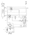
- Fig. 2a a second circuit implementation of the interface according to the invention is shown, which differs from the in Fig. 1a sketched embodiment differs only in that the switching between the two modes of protection T 1 is controlled by a discriminator circuit realized as a window comparator value-discriminated, which is the input side via the current limiting resistor R 1 with the analog signal U in acted upon.
- the digital output signal of the discriminator circuit forms the control signal U G1 of the circuit breaker T 1 .
- the discriminator circuit integrated in the transmitting branch 5 can be realized, for example, in connection with the controllable power switch T 1 or individually as an application-specific, monolithically integrated circuit component.
- the discriminator is then fed via a required for the operation of the supply voltage U v, in which, as in the present invention provided, may for example, be the signal dependent on the mains alternating voltage U mains or the digital bus voltage U bus signal U in. Thus, no additional power source is needed to power the discriminator circuit.
- the signal U in acted upon input K i 'of the discriminator circuit is connected to the live output line of an implemented as an RC element passive low-pass filter first order, consisting of the high-impedance input resistor R 1 and a formed between K i 'and the ground node of the interface filter capacitor C is formed and used for smoothing the guided to the input K i ' of the discriminator circuit and rectified mains AC voltage U network .
- Fig. 2b is the circuit construction of the present invention realized as a window comparator discriminator circuit for the embodiment of in Fig. 2a illustrated interface shown.
- the discriminator circuit which according to the invention is constructed from two comparator stages KP 1 and KP 2 connected to the signal inputs of an AND gate G, ensures that the control signal input K 2 of the circuit breaker T 1 is connected to the amplitude values via a digital control signal U G1 the derived from the AC mains voltage U network or derived from the digital bus voltage U bus analog signal U in depends, is discriminated value driven.
- an output side connected to a first signal input of the AND gate G first comparator KP 1 of the window comparator which is acted upon by an inverting input with the dependent of the AC mains voltage U network analog signal U in, serves to compare the amplitude values of this analog signal with the voltage potential a voltage applied to a non-inverting input of this first comparator KP 1, predeterminable reference voltage U as with a DC level of, for example 24 V.
- this first comparator stage supplied KP 1 via U in the energy required for operation.
- the second comparator stage KP 2 as well as the first comparator stage KP 1 are supplied via U in with the energy required for operation.
- a reverse polarity zener diode D z having a suitably defined breakdown voltage of, for example, 30 V, connected between the inverting input of the first comparator stage KP 1 connected to the non-inverting input of the second comparator stage KP 2 and the ground node of the interface circuit as an overvoltage protection.
- the second comparator stage KP 2 the conditions are different, since the roles of the two signals present at the non-inverting or inverting input of this comparator stage, as described above, are interchanged with those of the first comparator stage KP 1 .
- the amplitude values of the above-mentioned analog signal U in within a range of values between the voltage potential of the reference voltage U Su and the breakdown voltage of D Z "', takes the output voltage U out 2 of the second comparator stage KP 2, the voltage potential of its positive saturation voltage + U Sat to which (assuming positive logic) corresponds to a "high" level of U out 2 .
- a monostable multivibrator SR which is the digital control signal U G 1 of the circuit breaker T 1 , when a binary signal E 'with a "high” level at its input after a certain switching delay of a few nanoseconds duration from a stable "low” state (idle state) for a residence time ⁇ t' of a few milliseconds into an unstable "high” State before returning to its idle state by itself.
- a change of the input signal E 'during the dwell time .DELTA.t' has no effect on the switching state the monostable multivibrator SR.
- this univibrator ensures that even if the condition prescribed by the above inequality chain U su ⁇ U in ⁇ U for switching on the circuit breaker T 1, a short-circuiting of the mains voltage-carrying line via the transmitting branch 5 of the interface according to the invention is only possible for one by the residence time .DELTA.t 'of the monostable multivibrator SR predetermined time persists.
- the circuit breaker T 1 After returning the output signal A 'in the idle state of the univibrator SR, the circuit breaker T 1 is again caused to switch to the blocking state.
- the interface operates in compliance with the condition for only one of the residence time ⁇ t 'of the monostable multivibrator SR predetermined time in a DALI / DSI operating mode in which the supplied via the line-voltage-carrying line mains alternating voltage U Net z is shorted.
- the controllable power switch T 1 In order to cause the controllable power switch T 1 to switch to a safe operating mode with respect to the line voltage stability of the interface, it is only necessary to wait until the un-vibrator SR returns to its stable state.
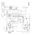
- Fig. 3a a third circuit realization of the interface according to the invention is shown, which differs from the in Fig. 1a and Fig. 2a sketched embodiments differs in that the switching between the two modes of protection circuit breaker T 1 is controlled by a built in the transmission branch 5 of the interface, constructed of discrete electronic components passive delay element with a delay, which acts on the input side with the AC mains voltage U network or the digital bus voltage U bus becomes.
- the passive delay element may include, for example, a first-order passive low-pass filter connected on the output side to the control signal input K 2 of the circuit breaker T 1 and the ground node of the interface, constituted by an RC element consisting of a gate capacitance C G 1 connected to the aforementioned ground node MOSFET realized circuit breaker T 1 and one between the control signal input of T 1 and the connection node between the constant current source KSQ and the primary branch of the transmitting side optocoupler 2 connected resistor R 2 (discharge resistor) is formed.
- the product of the gate capacitance C G 1 and the discharge resistor R 2 of the MOSFET T 1 forms a measure of the achievable switch-on delay time of its control signal U G. 1
- This time constant ⁇ can be dimensioned by a suitable dimensioning of the ohmic and capacitive components of the RC element so that the voltage potential at a via a current limiting resistor R 1 to the primary branch of the transmitting side optocoupler 2 and a in Reverse poled diode D to the control signal input K 2 of the circuit breaker T 1 connected nodes K 1 in the stop operation of the circuit breaker T1 faster the switching voltage of T 1 is reached when the voltage applied to its control signal input K 2 voltage potential U G. 1
- the effective resistance component of the total impedance of the RC element can, according to the invention, however, also be formed from the equivalent resistance of the parallel connection of the two ohmic resistors R 1 and R 2 which are connected at one end respectively to the primary branch of the transmitting-side opto-coupler 2 and at another end to the aforementioned one Node K 1 or to the control signal input K 2 of the circuit breaker T 1 are connected.
- the equivalent resistance value of the parallel circuit can be dimensioned by a suitable dimensioning of the two resistors R 1 and R 2 so that in the blocking operation of the circuit breaker, depending on the rms value of the rectified AC mains voltage U network , enough power to operate the transmitting side optocoupler 2 by the transmitting branch 5 flows.
- the control signal input K 2 of the circuit breaker T 1 is connected in this embodiment via the reverse polarity reversed protective diode D with another constant current source KSQ ', which keeps the current flowing through the parallel connection of the two resistors R 1 and R 2 current at an approximately constant level.
- a cathodically connected via a collector resistor R C 3 of a bipolar transistor T 3b required to operate this constant current source KSQ to the node K 1 and the anode side connected to the ground node of the interface, reverse biased Zener diode D Z 'with a suitably dimensioned breakdown voltage serves as overvoltage protection for the control signal input of T 1 .
- the two constant current sources KSQ and KSQ ' may comprise two mutually interacting bipolar transistors T 2a and T 2b (or T 3a and T 3b ) which are connected via their base electrodes to the collector or to the emitter of the respective other bipolar transistor and an ohmic resistor R E 2 ( R E 3 ) (emitter resistor) connected between the emitter electrodes of the respective bipolar transistors T 2a and T 2b (or T 3a and T 3b ).
- collector current I C 2b I C 3b
- collector current I C 2b I C 3b
- collector current I C 3b I C 3b
- collector resistance R C 2 ( R C 3 ) of the bipolar transistor T 2b (T 3b ) the emitter is raised in its voltage relative to the base of T 2b (T 3b ), which causes the base-emitter voltage U BE 2b ( U BE 3b ) of transistor T 2b (T 3b ) decreases.
- the constant current source KSQ holds in this way the current through the primary branch of the transmitting side optocoupler 2 current flowing at an approximately constant level, while the constant current source KSQ ', as already mentioned, serves to keep the current flowing through the parallel connection of the two ohmic resistors R 1 and R 2 current at an approximately constant level.
- Fig. 3b is a functionally equivalent circuit variant of in Fig. 3a illustrated interface, in which the discharge resistor R 2 of the RC element is not, as in Fig. 3a shown, as well as the current limiting resistor R 1 is connected to the connection node between the constant current source KSQ and the primary branch of the transmitting side optocoupler 2, but directly to the live output line of the full-wave rectifier.
- the discharge resistor R 2 of the RC element is not, as in Fig. 3a shown, as well as the current limiting resistor R 1 is connected to the connection node between the constant current source KSQ and the primary branch of the transmitting side optocoupler 2, but directly to the live output line of the full-wave rectifier. 8
Abstract
Description
Die Anmeldung betrifft eine Schnittstelle, der als zulässige Signale einerseits Digitalsignale und andererseits Signale von einem Taster oder Schalter an den gleichen eingangsseitigen Anschlüssen zugeführt werden können. Beide Signaltypen werden ausgangsseitig von der Schnittstelle derart weitergegeben, dass logische Zustände entsprechend dem logischen Zustand des jeweiligen eingangsseitigen Signals an eine Steuereinheit weitergegeben werden können. Da beide Signaltypen zulässig sind, darf beispielsweise auch das Anliegen eines Netzspannungspegels im Falle einer Taster- oder Schalter-Ansteuerung weder zu einer Zerstörung noch zu einer Abschaltung der Schnittstelle führen.The application relates to an interface that can be supplied as permissible signals on the one hand digital signals and on the other hand signals from a button or switch to the same input-side terminals. Both signal types are passed on the output side of the interface such that logical states can be passed to a control unit according to the logic state of the respective input-side signal. Since both types of signal are permitted, for example, the concern of a mains voltage level in the case of a push-button or switch control must lead neither to destruction nor to a shutdown of the interface.
Vorzugsweise weist die Schnittstelle auch einen Empfangszweig für Digitalsignale auf, die an den eingangsseitigen Anschlüssen der Schnittstelle an angeschlossene Busleitungen übertragen werden.Preferably, the interface also has a receiving branch for digital signals, which are transmitted to the input-side terminals of the interface to the connected bus lines.
Die ausgangsseitigen Signale der Schnittstelle können, wie gesagt, an eine Steuereinheit weitergegeben werden, die z.B. Teil eines Gebäudetechnikgeräts ist. Derartige Gebäudetechnikgeräte können z.B. Aktoren, Sensoren oder Betriebsgeräte für Leuchtmittel beinhalten. In diesem Zusammenhang bezieht sich die Erfindung insbesondere auf die Ansteuerung von dimmbaren Betriebsgeräten für Leuchtmittel, bei denen ein Dimmen sowohl durch Digitalsignale als auch durch Taster- oder Schaltersignale ausgelöst werden kann.The output signals of the interface can, as I said, be passed to a control unit, which is part of a building services equipment, for example. Such building technology devices may include, for example, actuators, sensors or operating devices for lighting. In this context, the invention relates in particular to the control of dimmable operating devices for lighting, in which a dimming can be triggered both by digital signals and by push-button or switch signals.
Die Erfindung hat sich zur Aufgabe gemacht, eine sichere Ausführung einer derartigen Schnittstelle mit verhältnismäßig wenigen elektronischen Bauteilen zu erreichen. Diese Aufgabe wird erfindungsgemäß durch die Merkmale der unabhängigen Ansprüche gelöst. Die abhängigen Ansprüche bilden den zentralen Gedanken der Erfindung in besonders vorteilhafter Weise weiter.The invention has set itself the task of achieving a safe execution of such an interface with relatively few electronic components. This object is achieved by the features of the independent claims. The dependent claims further form the central idea of the invention in a particularly advantageous manner.
Ein erster Aspekt der Erfindung betrifft eine Schnittstelle für Betriebsgeräte für Leuchtmittel. Die Schnittstelle weist dabei einen ersten Anschluss auf, an den wahlweise von einem mit Netzspannung versorgten Taster oder Schalter herstammende Signale oder Digitalsignale angelegt werden können, eine Signalverarbeitungsschaltung, die die jeweils angelegten Signale aufbereitet und an einem zweiten Anschluss zur Weitergabe an eine Steuereinheit eines angeschlossenen Betriebsgeräts zur Steuerung der Leuchtmittel entsprechend dem jeweils anliegenden Signal bereitstellt. Weiterhin ist eine Schutzschaltung vorgesehen, die eine Beschädigung der Schnittstelle bei eingangsseitigem Anliegen eines Netzspannungssignals verhindert. Im Normalzustand versetzt die Schutzschaltung die Signalverarbeitungsschaltung in einen Zustand, in dem sie zur Aufbereitung von Taster- oder Schaltersignalen konfiguriert ist. Nur wenn die Schutzschaltung während einer vorbestimmten Zeitdauer an dem ersten Anschluss kein Anliegen eines Netzspannungssignals erfasst, versetzt sie die Signalverarbeitungsschaltung in einen Zustand, in dem Letztere zur Aufbereitung von Digitalsignalen konfiguriert ist. Die vorbestimmte Zeitdauer kann dabei wenigstens so lang wie eine Halbwelle der Netzspannung sein.A first aspect of the invention relates to an interface for operating devices for lighting. In this case, the interface has a first connection, to which signals or digital signals originating either from a mains-powered pushbutton or switch can be applied, a signal processing circuit which processes the respectively applied signals and at a second connection for transmission to a control unit of a connected operating device provides for controlling the lighting means according to the respective applied signal. Furthermore, a protection circuit is provided which prevents damage to the interface at the input-side concern of a mains voltage signal. In the normal state, the protection circuit sets the signal processing circuit in a state in which it is configured for the preparation of push-button or switch signals. Only when the protection circuit does not detect a presence of a mains voltage signal at the first terminal for a predetermined period of time does it place the signal processing circuit in a state where the latter is configured to process digital signals. The predetermined period of time can be at least as long as a half-wave of the mains voltage.
Die Schutzschaltung, bei der es sich z.B. um eine integrierte Schaltung handeln kann, kann die Schnittstelle unverzüglich für Netzspannungssignale konfigurieren, wenn sie ein Anliegen eines Netzspannungssignals erfasst.The protection circuit, which may be an integrated circuit, for example, can immediately configure the interface for line voltage signals when it is on Concerns a mains voltage signal detected.
Zur Konfigurierung der Schnittstelle für Netzspannungssignale kann ein Strombegrenzungswiderstand geschaltet sein, der durch die Schutzschaltung zur Konfigurierung der Schnittstelle für Digitalsignale durch Schließen eines Schutzschalters überbrückt wird. Der Schalter ist dabei derart ausgelegt, dass die Abschaltung der Netzspannung auf jeden Fall schneller erfolgt als die Netzspannung über einen definierten Referenzspannungspegel ansteigen kann. Darüber hinaus ist der Strombegrenzungswiderstand zur Sicherheit gegen ein dauerhaftes Anliegen der Netzspannung an den Eingangsanschlüssen der Schnittstelle so hochohmig dimensioniert, dass er eine derartige Störung absorbieren kann.To configure the interface for mains voltage signals, a current limiting resistor may be connected, which is bypassed by the protective circuit for configuring the interface for digital signals by closing a circuit breaker. The switch is designed such that the shutdown of the mains voltage takes place in any case faster than the mains voltage can rise above a defined reference voltage level. In addition, the current limiting resistor for safety against a permanent concern of the mains voltage at the input terminals of the interface is so high-impedance dimensioned that it can absorb such a fault.
Zu dem Strombegrenzungswiderstand kann eine Konstantstromquelle parallel geschaltet sein, die in Serie zu dem Schutzschalter geschaltet ist, um bei eingangsseitigem Anliegen der Digitalsignale einen definierten Stromfluss zu erzeugen.To the current limiting resistor, a constant current source may be connected in parallel, which is connected in series with the circuit breaker to generate a defined current flow at the input-side concern of the digital signals.
Der Schutzschalter kann z.B. ein Transistor sein, der optional zusammen mit der Schutzschaltung als integrierte Schaltung ausgeführt ist.The circuit breaker may e.g. a transistor which is optionally designed together with the protection circuit as an integrated circuit.
Auch die beiden Optokoppler (2, 3) und der Gleichrichter können mit in eine Schaltung integriert sein.The two optocouplers (2, 3) and the rectifier can be integrated into a circuit.
Somit kann die gesamte Schnittstellenschaltung als integrierte Schaltung in ein Standard-IC-Gehäuse aufgenommen werden, was sehr platzsparend ist. Dies ist vor allem für ein LED-Betriebsgerät von Vorteil.Thus, the entire interface circuit can be incorporated as an integrated circuit in a standard IC package, which is very space-saving. This is especially advantageous for a LED control gear.
Die Schnittstelle kann weiterhin einen mit dem ersten Anschluss verbindbaren Empfangszweig für Digitalsignale aufweisen, die der Schnittstelle von der Steuereinheit eines angeschlossenen Betriebsgeräts zuführbar sind.The interface can furthermore have a reception branch for digital signals, which can be connected to the first connection, which can be supplied to the interface of the control unit of a connected operating device.
Darüber hinaus kann die Schnittstelle eine Potentialtrennungseinheit (z.B. einen Optokoppler) aufweisen, der primärseitig mit dem ersten Anschluss und sekundärseitig mit dem zweiten Anschluss verbunden ist.In addition, the interface may include a potential separation unit (e.g., an optocoupler) connected on the primary side to the first terminal and on the secondary side to the second terminal.
Die Schutzschaltung kann ferner einen Microcontroller aufweisen, dessen Funktion weiter unten im Detail erläutert wird.The protection circuit may further comprise a microcontroller whose function will be explained in detail below.
Die Erfindung bezieht sich außerdem auf ein System, welches eine Schnittstelle des oben geschilderten Typs und ein Betriebsgerät für Leuchtmittel oder ein anderes steuerbares Gebäudetechnikgerät aufweist. Bei dem Betriebsgerät kann es sich z.B. um ein Vorschaltgerät für Gasentladungslampen oder LEDs handeln.The invention also relates to a system having an interface of the type described above and an operating device for lighting or other controllable building services equipment. The operating device may be e.g. to act a ballast for gas discharge lamps or LEDs.
Darüber hinaus bezieht sich die Erfindung auch auf ein Verfahren zum Betrieb einer Schnittstelle für Betriebsgeräte zur Ansteuerung von Leuchtmitteln, wobei die Schnittstelle einen ersten Anschluss aufweist, an den wahlweise von einem mit Netzspannung versorgten Taster oder Schalter herstammende Signale oder Digitalsignale angelegt werden können, eine Signalverarbeitungsschaltung, die die jeweils angelegten Signale aufbereitet und an einem zweiten Anschluss zur Weitergabe an eine Steuereinheit eines angeschlossenen Betriebsgeräts zur Steuerung der Leuchtmittel entsprechend dem jeweils anliegenden Signal bereitstellt. Im Normalzustand wird die Signalverarbeitungsschaltung in einen Zustand versetzt, in dem sie zur Aufbereitung von Taster- oder Schaltersignalen konfiguriert ist. Nur wenn während einer vorbestimmten Zeitdauer an dem ersten Anschluss kein Anliegen eines Netzspannungssignals erfasst wird, wird die Signalverarbeitungsschaltung in einen Zustand versetzt, in dem sie zur Aufbereitung von Digitalsignalen konfiguriert ist.In addition, the invention also relates to a method for operating an interface for operating devices for controlling lighting means, wherein the interface has a first terminal, to which either from a supplied with mains power button or switch originating signals or digital signals can be applied, a signal processing circuit , which processes the respectively applied signals and provides them at a second connection for transmission to a control unit of a connected operating device for controlling the lighting means in accordance with the respective applied signal. In the normal state, the signal processing circuit is set in a state in which it is configured for the preparation of push-button or switch signals. Only if for a predetermined period of time at the first port no concern a Mains voltage signal is detected, the signal processing circuit is placed in a state in which it is configured for conditioning of digital signals.
Weitere Merkmale, Vorteile und Eigenschaften der vorliegenden Erfindung sollen nunmehr Bezug nehmend auf die begleitenden Zeichnungen näher erläutert werden.
- Fig. 1a
- zeigt eine erste schaltungstechnische Realisierung der erfindungsgemäßen Schnittstelle mit einem angeschlossenen Betriebsgerät für ein Leuchtmittel,
- Fig. 1b
- zeigt eine schematische Darstellung eines digitalen Zeitschaltglieds mit Anzugsverzögerung, das als integrierte Schutzschaltung zum Schalten eines zwischen zwei verschiedenen Betriebsarten umschaltenden steuerbaren Leistungsschalters Teil der in
Fig. 1a dargestellten Schnittstelle sein kann, - Fig. 2a
- zeigt eine zweite schaltungstechnische Realisierung der erfindungsgemäßen Schnittstelle mit einem angeschlossenen Betriebsgerät für ein Leuchtmittel,
- Fig. 2b
- zeigt den Schaltungsaufbau einer als Fensterkomparator realisierten Diskriminatorschaltung, die als integrierte Schutzschaltung zum Schalten eines zwischen zwei verschiedenen Betriebsarten umschaltenden steuerbaren Leistungsschalters Teil der in
Fig. 1b dargestellten Schnittstelle sein kann, - Fig. 3a
- zeigt eine dritte schaltungstechnische Realisierung der erfindungsgemäßen, zur Ansteuerung eines Betriebsgeräts für ein Leuchtmittel verwendeten Schnittstelle mit einem zum Umschalten zwischen einer getasteten Netzwechselspannung und einem digitalen Busspannungssignal dienenden steuerbaren Leistungsschalter, der über ein aus diskreten elektronischen Bauelementen gebildetes passives Verzögerungsglied erster Ordnung zeitverzögert angesteuert wird, und
- Fig. 3b
- zeigt eine funktionsäquivalente Schaltungsvariante der in
Fig. 3a skizzierten Schnittstelle.
- Fig. 1a
- shows a first circuit realization of the interface according to the invention with a connected operating device for a light source,
- Fig. 1b
- shows a schematic representation of a digital timing element with a pickup delay, which serves as an integrated protection circuit for switching a switchable between two different modes controllable power switch part of in
Fig. 1a represented interface can be - Fig. 2a
- shows a second circuit realization of the interface according to the invention with a connected operating device for a lamp,
- Fig. 2b
- shows the circuit structure of a discriminator circuit realized as a window comparator, which is part of the in FIG. 1 as integrated protection circuit for switching a controllable power switch which switches over between two different operating modes
Fig. 1b represented interface can be - Fig. 3a
- shows a third circuit realization of the invention used to control an operating device for a light emitting interface with a serving for switching between a sampled AC line voltage and a digital bus voltage signal controllable power switch, which is controlled by a time delay formed from a discrete electronic components passive delay element of the first, and
- Fig. 3b
- shows a functionally equivalent circuit variant of in
Fig. 3a sketched interface.
In
Üblicherweise ist die Information bei Taster- oder Schaltersignalen zeitkontinuierlich über die Dauer der jeweiligen vorzugsweise manuellen Betätigung codiert. Taster- oder Schaltersignale sind daher im Vergleich zu Digitalsignalen von wesentlich niedrigerer Frequenz.Usually, the information is coded on the button or switch signals continuous time over the duration of the respective preferably manual operation. Push-button or switch signals are therefore of significantly lower frequency compared to digital signals.
Digitalsignale sind über hochfrequente Schaltvorgänge codiert.Digital signals are encoded via high-frequency switching operations.
Das Anliegen dieser Netzwechselspannung U Netz darf dabei weder zu einem Abschalten noch zu einer Zerstörung oder sonstigen Beeinträchtigung der Schnittstelle führen. Vielmehr muss die Schnittstelle in der Lage sein, unabhängig von dem Anliegen der beiden Signaltypen ein entsprechendes Logiksignal an einem sendeseitigen Ausgangsanschluss KS bereitzustellen, das beispielsweise zu einem zur Ansteuerung eines Leuchtmittels 7 verwendeten Betriebsgerät 6 weitergegeben werden kann. Im Falle von Tastersignalen wertet eine Steuereinheit des Betriebsgeräts 6 z.B. die Anzahl und/oder die Dauer der jeweiligen Tasterbetätigung aus und erzeugt daraus Ansteuersignale für das angeschlossene Leuchtmittel 7.The concern of this mains AC voltage U network must neither lead to a shutdown nor to destruction or other impairment of the interface. Rather, the interface must be able to provide a corresponding logic signal at a transmitting-side output terminal K S , regardless of the concerns of the two signal types, which can be forwarded to an
Baulich kann die Schnittstelle von dem Betriebsgerät 6 getrennt oder aber auch in das gleiche Gehäuse oder sogar auf der gleichen Platine integriert sein.Structurally, the interface can be separate from the operating
Die Schnittstelle benötigt keine eigene separate Spannungsversorgung. Eine Spannungsversorgung kann indessen über die eingangsseitigen Anschlüsse erfolgen, da der Ruhepegel (logisch "Null") beim DALI-Standard ungleich 0 Volt gewählt ist.The interface does not require its own separate power supply. However, a voltage supply can be done via the input-side connections, since the quiescent level (logic "zero") is selected at the DALI standard not equal to 0 volts.
Der Sendezweig ist in
An die Eingangsklemmen K-K' schließt sich eine Filter- und Überspannungsschutzschaltung 1 an, die eine Drosselspule und einen spannungsabhängigen Widerstand VDR aufweist. Auf diese Filter- und Überspannungsschutzschaltung 1 folgt ein Gleichrichter 8 in Form einer Vollbrücke. Bei Anliegen einer Netzspannung UNetz an den Eingangsklemmen K-K' liefert der Gleichrichter also eine gleichgerichtete Wechselspannung mit einer Frequenz von beispielsweise 100 Hz.To the input terminals KK 'is followed by a filter and
Das Ausgangssignal des Gleichrichters 8 wird einem Optokoppler 2 zugeführt, der zur Potentialtrennung zwischen den ausgangsseitigen Anschluss KS des Sendezweigs und den externen Anschlüssen K-K' der Schnittstelle dient. In Serie zu dem Optokoppler 2 ist eine Konstantstromquelle KSQ geschaltet. Wenn nun an den eingangsseitigen Anschlüssen K-K' ein Digitalsignal mit einem maximalen "High"-Pegel von beispielsweise 30 V anliegt, fließt ein Strom durch den Optokoppler 2, der durch die Konstantstromquelle KSQ vorgegeben ist und der ausreichend gewählt ist, um die Ansprechschwelle des Optokopplers 2 zu überschreiten, so dass ausgangsseitig ein entsprechendes Logiksignal an dem Anschluss KS ausgegeben wird.The output signal of the rectifier 8 is fed to an
Wenn nun in diesem Zustand indessen ein Netzspannungssignal an die Klemmen K-K' angelegt werden würde, wäre aufgrund der hohen Spannungspegel eine Beschädigung der Primärseite des Optokopplers 2 zu befürchten. Daher ist vorgesehen, dass als Grundeinstellung in Serie zum Primärzweig des Optokopplers 2 ein hochohmiger Widerstand R 1 (Schutz- oder Strombegrenzungswiderstand) geschaltet ist. Dieser Widerstand R 1 ist derart dimensioniert, dass bei Anliegen einer Spannung (z.B. einer Netzspannung) an den Anschlüssen K-K' ein Strom durch den Widerstand R 1 und somit auf den Optokoppler 2 primärseitig fließt, der einerseits wiederum die Ansprechschwelle des Optokopplers 2 überschreitet, andererseits aber klein genug ist, um eine Beschädigung des Optokopplers 2 oder anderer Bauteile der Schnittstelle zu vermeiden.If, however, a mains voltage signal would now be applied to the terminals KK 'in this state, damage to the primary side of the
Der Strombegrenzungswiderstand R 1 wird dabei selektiv in Serie zu dem Optokoppler 2 geschaltet und kann selektiv mittels eines Schutzschalters T1 überbrückt werden. Der Schutzschalter stellt also eine Möglichkeit dar, aktiv zwischen einer Konfigurierung "Digitalsignal" (als Grundeinstellung) und "Tastersignal" (wenn bestimmte Bedingungen erfüllt sind) bzw. umgekehrt zu schalten, wobei dieses aktive Überführen auf Grundlage einer Erfassung und Auswertung der eingangsseitigen Spannungspegel erfolgt.The current limiting resistor R 1 is selectively connected in series with the
Bei dem Schutzschalter T1 kann es sich insbesondere um einen hochspannungsfesten npn-Bipolartransistor oder MOS-Feldeffekttransistor handeln.The circuit breaker T 1 may in particular be a high-voltage-resistant npn bipolar transistor or MOS field-effect transistor.
Der Schutzschalter T1 ist dabei Teil einer Schutzschaltung 9, die eine Steuereinheit µC1 aufweist. Die Steuereinheit µC1 steuert aktiv durch Ausgabe eines Schaltsignals, z.B. der Gate-Spannung U G1 eines MOSFETs, den Schutzschalter T1 an. Die Steuereinheit µC1 kann eine integrierte Schaltung, wie beispielsweise Mikrocontroller sein. Zusammen mit dieser Steuereinheit kann auch der Schutzschalter T1 als Transistor mit integriert sein. Die Schutzschaltung kann also diskret aufgebaut und/oder Software-gesteuert sein.The circuit breaker T 1 is part of a
Auch die beiden Optokoppler 2, 3 und der Gleichrichter können mit in eine Schaltung integriert sein.The two
Somit kann die gesamte Schnittstellenschaltung als integrierte Schaltung in ein Standard-IC-Gehäuse aufgenommen werden, was sehr platzsparend ist. Dies ist vor allem für ein LED-Betriebsgerät von Vorteil.Thus, the entire interface circuit can be incorporated as an integrated circuit in a standard IC package, which is very space-saving. This is especially advantageous for a LED control gear.
Der Steuereinheit µC1 wird ebenfalls das an den externen Anschlüssen K-K' der Schnittstelle anliegende Signal zugeführt. Somit erfasst die Steuereinheit µC1 der Schutzschaltung 9, ob ein potentiell gefährliches Netzspannungssignal an den Anschlüssen K-K' anliegt.The control unit .mu.C 1 is also supplied with the signal applied to the external terminals KK 'of the interface. Thus, the control unit μC 1 of the
Erfindungsgemäß ist nunmehr vorgesehen, dass als Grundeinstellung der Schalter T1 geöffnet ist, dass also der hochohmiger Widerstand R 1 in Serie zum Primärzweig des Optokopplers 2 geschaltet ist. Die Steuereinheit µC1 schließt den Schalter T1 nur, wenn während einer vorbestimmten Zeitdauer festgestellt wurde, dass kein Netzspannungssignal an den Anschlüssen K-K' anliegt. Diese Zeitdauer ist dabei so gewählt, dass sie wenigstens der Zeitdauer einer halben Periode der Netzspannung beträgt.According to the invention, provision is now made for the switch T 1 to be open as the basic setting, ie for the high-resistance resistor R 1 to be connected in series with the primary branch of the opto-
Das Überbrücken des Strombegrenzungswiderstands R 1 findet dabei erst dann zeitverzögert statt, wenn sicher keine Netzspannung anliegt. Falls dagegen bei geschlossenem Schalter T1 das Anliegen einer Netzspannung erfasst wird, wird der Schalter T1 wieder sofort geöffnet, um den Strombegrenzungswiderstand R 1 wieder in Serie zu dem Optokoppler 2 zu schalten.The bridging of the current limiting resistor R 1 takes place only after a time delay, when certainly no mains voltage is applied. If, on the other hand, when the switch T 1 is closed, the presence of a mains voltage is detected, the switch T 1 is again opened immediately to the current limiting resistor R 1 again in series with the
Im Übrigen schützt diese Schutzschaltung durch den genannten Mechanismus auch den Empfangszweig davor, dass er aktiviert wird, während ein Netzspannungssignal anliegt.Moreover, this protective circuit also protects the receiving branch from being activated while a mains voltage signal is applied by the said mechanism.
Genauer gesagt wird das unverzögerte Signal U in dem nicht-invertierenden Eingang eines Komparators KP zugeführt, an dessen invertierendem Eingang eine Referenzspannung U So mit einem Gleichspannungspegel von z.B. 22 V anliegt, also einem Pegel, der etwas niedriger gewählt ist als der maximal zulässige Hochpegel des digitalen Bussignals.More specifically, the undelayed signal U in the non-inverting input of a comparator KP is supplied to the inverting input of a reference voltage U So is applied with a DC level of, for example 22 V, that is, a level which is slightly lower than the maximum allowable high level of digital bus signal.
Da es sich bei dem Rücksetzeingang R1 des RS-Flipflops FF um einen dominierenden Rücksetzeingang handelt, das Rücksetzsignal am Eingang R1 der bi-stabilen Kippstufe also Priorität hat, wird das Ausgangssignal des RS-Flipflops FF ohne zeitliche Verzögerung auf "logisch Null" gesetzt, so dass entsprechend der Schalter T1 wieder geöffnet wird.Since the reset input R1 of the RS flip-flop FF is a dominant reset input, the reset signal at the input R1 of the bistable flip-flop has priority, the output signal of the RS flip-flop FF is set to "logical zero" without a time delay. so that according to the switch T 1 is opened again.
In
Die Diskriminatorschaltung wird dabei über eine zum Betrieb erforderliche Versorgungsspannung U v gespeist, bei der sich, wie erfindungsgemäß vorgesehen, z.B. um das von der Netzwechselspannung U Netz bzw. von der digitalen Busspannung U Bus abhängige Signal U in handeln kann. Somit wird keine zusätzliche Spannungsquelle zur Spannungsversorgung der Diskriminatorschaltung benötigt.The discriminator is then fed via a required for the operation of the supply voltage U v, in which, as in the present invention provided, may for example, be the signal dependent on the mains alternating voltage U mains or the digital bus voltage U bus signal U in. Thus, no additional power source is needed to power the discriminator circuit.
Darüber hinaus kann bei diesem Ausführungsbeispiel optional vorgesehen sein, dass der mit dem Signal U in beaufschlagte Eingang Ki' der Diskriminatorschaltung mit der spannungsführenden Ausgangsleitung eines als RC-Glied realisierten passiven Tiefpassfilters erster Ordnung verbunden ist, das aus dem hochohmigen Eingangswiderstand R 1 und einem zwischen Ki' und den Masseknoten der Schnittstelle geschalteten Filterkondensator C gebildet wird und zur Glättung der auf den Eingang Ki' der Diskriminatorschaltung geführten getasteten und gleichgerichteten Netzwechselspannung U Netz dient.In addition, it can optionally be provided in this embodiment that the signal U in acted upon input K i 'of the discriminator circuit is connected to the live output line of an implemented as an RC element passive low-pass filter first order, consisting of the high-impedance input resistor R 1 and a formed between K i 'and the ground node of the interface filter capacitor C is formed and used for smoothing the guided to the input K i ' of the discriminator circuit and rectified mains AC voltage U network .
In
Eine ausgangsseitig mit einem zweiten Signaleingang des UND-Gatters G verbundene zweite Komparatorstufe KP2 des Fensterkomparators, die über einen nicht-invertierenden Eingang mit dem von der Netzwechselspannung U Netz abhängenden Analogsignal U in beaufschlagt wird, dient zum Vergleich der Amplitudenwerte dieses Analogsignals mit dem Spannungspotenzial einer an einem invertierenden Eingang dieser zweiten Komparatorstufe KP2 anliegenden, vorgebbaren Referenzspannung U Su mit einem Gleichspannungspegel von beispielsweise 5 V. Dabei wird die zweite Komparatorstufe KP2 erfindungsgemäß ebenso wie die erste Komparatorstufe KP1 über U in mit der zum Betrieb benötigten Energie versorgt. Eine in Sperrrichtung gepolte Zenerdiode Dz"' mit einer geeignet festgelegten Durchbruchspannung von beispielsweise 30 V, welche zwischen den mit dem nicht-invertierenden Eingang der zweiten Komparatorstufe KP2 verbundenen invertierenden Eingang der ersten Komparatorstufe KP1 und den Masseknoten der Schnittstellenschaltung geschaltet ist, dient dabei als Überspannungsschutz.An output side connected to a second signal input of the AND gate G second comparator stage KP 2 of the window comparator, which is acted upon by a non-inverting input with the dependent of the AC mains voltage U network analog signal U in , is used to compare the amplitude values of this analog signal with the voltage potential a predefinable reference voltage U Su applied to an inverting input of this second comparator stage KP 2 with a DC voltage level of, for example, 5 V. According to the invention, the second comparator stage KP 2 as well as the first comparator stage KP 1 are supplied via U in with the energy required for operation. A reverse polarity zener diode D z "having a suitably defined breakdown voltage of, for example, 30 V, connected between the inverting input of the first comparator stage KP 1 connected to the non-inverting input of the second comparator stage KP 2 and the ground node of the interface circuit as an overvoltage protection.
Liegen die Amplitudenwerte des vorgenannten Analogsignals U in unterhalb des Spannungspotenzials der Referenzspannung U So oder oberhalb der Durchbruchspannung von DZ"', nimmt die Ausgangsspannung U out1 der ersten Komparatorstufe KP1 das Spannungspotenzial ihrer positiven Sättigungsspannung + U sat an, welche (positive Logik vorausgesetzt) einem "High"-Pegel von U out1 entspricht. Liegen die Amplitudenwerte des vorgenannten Analogsignals U in dagegen in einem Wertebereich zwischen dem Spannungspotenzial der Referenzspannung U so und der Durchbruchspannung von DZ"', nimmt die Ausgangsspannung U out1 der ersten Komparatorstufe KP1 das Spannungspotenzial ihrer negativen Sättigungsspannung - U sat an, welche (wiederum positive Logik vorausgesetzt) einem "Low"-Pegel von U out1 entspricht.Are the amplitude values of the above-mentioned analog signal U in below the voltage potential of the reference voltage U way or above the breakdown voltage of D Z "', 1 the output voltage U out 1 of the first comparator CP, the voltage potential of its positive saturation voltage + U sat at which (positive logic provided) corresponds to a "high" level of U out 1. If the amplitude values of the aforementioned analog signal U in lie in a value range between the voltage potential of the reference voltage U so and the breakdown voltage of D Z "', the output voltage U out 1 of the first decreases Comparator stage KP 1, the voltage potential of their negative saturation voltage - U sat , which (assuming positive logic) corresponds to a "low" level of U out 1 .
Bei der zweiten Komparatorstufe KP2 liegen die Verhältnisse anders, da die Rollen der beiden an dem nicht-invertierenden bzw. invertierenden Eingang dieser Komparatorstufe anliegenden Signale, wie vorstehend beschrieben, gegenüber denen der ersten Komparatorstufe KP1 vertauscht sind. Liegen die Amplitudenwerte des vorgenannten Analogsignals U in innerhalb eines Wertebereichs zwischen dem Spannungspotenzial der Referenzspannung U Su und der Durchbruchspannung von DZ"', nimmt die Ausgangsspannung U out2 der zweiten Komparatorstufe KP2 das Spannungspotenzial ihrer positiven Sättigungsspannung + U Sat an, welche (positive Logik vorausgesetzt) einem "High"-Pegel von U out2 entspricht. Liegen die Amplitudenwerte des vorgenannten Analogsignals U in dagegen unterhalb des Spannungspotenzials der Referenzspannung U Su oder oberhalb der Durchbruchspannung von DZ''', nimmt die Ausgangsspannung U out2 der zweiten Komparatorstufe KP2 das Spannungspotenzial ihrer negativen Sättigungsspannung - U Sat an, die (wiederum positive Logik vorausgesetzt) einem "Low"-Pegel von U out2 entspricht.In the case of the second comparator stage KP 2 , the conditions are different, since the roles of the two signals present at the non-inverting or inverting input of this comparator stage, as described above, are interchanged with those of the first comparator stage KP 1 . Are the amplitude values of the above-mentioned analog signal U in within a range of values between the voltage potential of the reference voltage U Su and the breakdown voltage of D Z "', takes the output voltage U out 2 of the second comparator stage KP 2, the voltage potential of its positive saturation voltage + U Sat to which (assuming positive logic) corresponds to a "high" level of U out 2 . Are the amplitude values of the above-mentioned analog signal U in the other hand, below the voltage potential of the reference voltage U Su or above the breakdown voltage of D Z ''', the output voltage U 2 takes out 2 of the second comparator stage KP, the voltage potential of its negative saturation voltage - U satellite, which ( again assuming positive logic) corresponds to a "low" level of U out 2 .
Da über den Ausgang des UND-Gatters G nur dann ein Binärsignal mit einem "High"-Pegel bereitgestellt wird, wenn beide Eingangssignale dieses UND-Gatters, bei denen es sich um die beiden digitalen Ausgangsspannungen U out1 bzw. U out2 der Komparatorstufen KP1 und KP2 handelt, "High"-Pegel führen, befindet sich der Schutzschalter T1 nur dann in einem Durchschaltbetrieb, wenn die Amplitudenwerte des Analogsignals U in dem Betrage nach in den durch die beiden Referenzspannungen U Su und U So des Fensterkomparators begrenzten Wertebereich hineinfallen und damit die Ungleichungskette U Su < U in < U So erfüllt ist. Wie aus
Nach dem Zurückkehren des Ausgangssignals A' in den Ruhezustand des Univibrators SR wird der Schutzschalter T1 wieder zum Umschalten in den Sperrzustand veranlasst. Die Schnittstelle arbeitet bei Einhaltung der Bedingung also nur für eine durch die Verweildauer Δt' der monostabilen Kippstufe SR vorgegebene Zeit in einem DALI/DSI-Betriebsmodus, in dem die über die netzspannungsführende Leitung bereitgestellte Netzwechselspannung U Netz kurzgeschlossen ist. Um den steuerbaren Leistungsschalter T1 zum Umschalten in einen in Bezug auf die Netzspannungsfestigkeit der Schnittstelle sicheren Betriebsmodus zu veranlassen, braucht lediglich abgewartet zu werden, bis der Univibrator SR wieder seinen stabilen Zustand annimmt.After returning the output signal A 'in the idle state of the univibrator SR, the circuit breaker T 1 is again caused to switch to the blocking state. Thus, the interface operates in compliance with the condition for only one of the residence time Δ t 'of the monostable multivibrator SR predetermined time in a DALI / DSI operating mode in which the supplied via the line-voltage-carrying line mains alternating voltage U Net z is shorted. In order to cause the controllable power switch T 1 to switch to a safe operating mode with respect to the line voltage stability of the interface, it is only necessary to wait until the un-vibrator SR returns to its stable state.
Ist die durch die vorstehende Ungleichungskette vorgegebene Bedingung nicht erfüllt, wird am Ausgang des UND-Gatters G ein Binärsignal mit einem "Low"-Pegel bereitgestellt, der unverändert auf den Ausgang der monostabilen Kippstufe SR weitergeschaltet wird, was dazu führt, dass der Schutzschalter T1 in diesem Falle sperrt und die netzspannungsführende Leitung nicht über den Sendezweig 5 der erfindungsgemäßen Schnittstelle kurzgeschlossen wird. Dies führt dazu, dass die Schnittstelle in einem Betriebsmodus verbleibt, in dem die an ihrem Netzspannungseingang K-K' anliegende Netzwechselspannung U Nets nicht über T1 kurzgeschlossen werden kann.If the condition specified by the above inequality chain is not satisfied, a binary signal having a "low" level is provided at the output of the AND gate G, which is passed on unchanged to the output of the monostable multivibrator SR, which results in the circuit breaker T 1 blocks in this case and the mains voltage-carrying line is not short-circuited via the transmitting
In dieser Betriebsart ist nur über den hochohmigen Eingangswiderstand R 1 der Schutzschaltung 9, den Primärzweig des sendeseitigen Optokopplers 2 sowie über den Sekundärzweig des empfangsseitigen Optokopplers 3 ein Stromfluss möglich.In this mode of operation, current flow is possible only via the high-impedance input resistor R 1 of the
In
Diese Zeitkonstante τ kann dabei durch eine geeignete Dimensionierung der ohmschen und kapazitiven Bauelemente des RC-Glieds so bemessen sein, dass das Spannungspotenzial an einem über einen Strombegrenzungswiderstand R 1 mit dem Primärzweig des sendeseitigen Optokopplers 2 und über eine in Sperrrichtung gepolte Diode D mit dem Steuersignaleingang K2 des Schutzschalters T1 verbundenen Knoten K1 im Sperrbetrieb des Schutzschalters T1 schneller die Schaltspannung von T1 erreicht als das an dessen Steuersignaleingang K2 anliegende Spannungspotenzial von U G1 . This time constant τ can be dimensioned by a suitable dimensioning of the ohmic and capacitive components of the RC element so that the voltage potential at a via a current limiting resistor R 1 to the primary branch of the transmitting
Der Wirkwiderstandsanteil der Gesamtimpedanz des RC-Glieds kann erfindungsgemäß aber auch aus dem äquivalenten Widerstandswert der Parallelschaltung der beiden Ohmschen Widerstände R1 und R2 gebildet werden, die an einem Ende jeweils mit dem Primärzweig des sendeseitigen Optokopplers 2 und an einem anderen Ende mit dem vorgenannten Knoten K1 bzw. mit dem Steuersignaleingang K2 des Schutzschalters T1 verbunden sind. Der äquivalente Widerstandswert der Parallelschaltung kann dabei durch eine geeignete Dimensionierung der beiden Ohmschen Widerstände R1 und R2 so bemessen sein, dass im Sperrbetrieb des Schutzschalters, abhängig vom Effektivwert der gleichgerichteten Netzwechselspannung U Netz, genügend Strom zum Betrieb des sendeseitigen Optokopplers 2 durch den Sendezweig 5 fließt.The effective resistance component of the total impedance of the RC element can, according to the invention, however, also be formed from the equivalent resistance of the parallel connection of the two ohmic resistors R 1 and R 2 which are connected at one end respectively to the primary branch of the transmitting-side opto-
Der Steuersignaleingang K2 des Schutzschalters T1 ist bei diesem Ausführungsbeispiel über die in Sperrrichtung gepolte Schutzdiode D mit einer weiteren Konstantstromquelle KSQ' verbunden, die den über die Parallelschaltung der beiden Ohmschen Widerstände R 1 und R 2 fließenden Strom auf einem näherungsweise konstanten Niveau hält. Eine kathodenseitig über einen Kollektorwiderstand R C3 eines zum Betrieb dieser Konstantstromquelle KSQ' benötigten Bipolartransistors T3b mit dem Knoten K1 und anodenseitig mit dem Masseknoten der Schnittstelle verbundene, in Sperrrichtung gepolte Zenerdiode DZ' mit einer geeignet dimensionierten Durchbruchspannung dient dabei als Überspannungsschutz für den Steuersignaleingang von T1.The control signal input K 2 of the circuit breaker T 1 is connected in this embodiment via the reverse polarity reversed protective diode D with another constant current source KSQ ', which keeps the current flowing through the parallel connection of the two resistors R 1 and R 2 current at an approximately constant level. A cathodically connected via a collector resistor R C 3 of a bipolar transistor T 3b required to operate this constant current source KSQ to the node K 1 and the anode side connected to the ground node of the interface, reverse biased Zener diode D Z 'with a suitably dimensioned breakdown voltage serves as overvoltage protection for the control signal input of T 1 .
Da die beiden Konstantstromquellen KSQ und KSQ' in dem skizzierten Ausführungsbeispiel gleich aufgebaut sind, werden sie im Folgenden gemeinsam beschrieben, wobei sich die nicht eingeklammerten Bezugszeichen auf die elektronischen Bauelemente der Konstantstromquelle KSQ beziehen und die in runden Klammern angegebenen Bezugszeichen auf die elektronischen Bauelemente der baugleichen Konstantstromquelle KSQ'. Wie in
Bei einem Anstieg des durch T2b (T3b) fließenden Kollektorstroms I C2b ( I C3b), bei dem es sich um einen durch einen Spannungsabfall der amplitudengetasteten und gleichgerichteten Netzwechselspannung U Netz bzw. um einen Spannungsabfall der digitalen Busspannung U Bus an einem Kollektorwiderstand R C2 (R C3) des Bipolartransistors T2b (T3b) hervorgerufenen Strom handelt, wird der Emitter in seiner Spannung gegenüber der Basis von T2b (T3b) angehoben, was dazu führt, dass die Basis-Emitter-Spannung U BE2b ( U BE3b) von Transistor T2b (T3b) sinkt. Dies steuert den Bipolartransistor T2b (T3b) in einen hochohmigen Zustand und lässt den Kollektorstrom I c2b ( I c3b) sofort wieder sinken. Bei einer Abnahme des Kollektorstroms I c2b ( I c3b) wird dagegen die Basis-Emitter-Spannung U BE2b ( U BE3b) größer, wodurch T2b (T3b) in einen niederohmigen Zustand gesteuert wird und der Kollektorstrom I c2b ( I c3b) wieder ansteigt. Die Konstantstromquelle KSQ hält auf diese Weise die Stromstärke des durch den Primärzweig des sendeseitigen Optokopplers 2 fließenden Stroms auf einem näherungsweise konstanten Niveau, während die Konstantstromquelle KSQ', wie bereits erwähnt, dazu dient, den über die Parallelschaltung der beiden Ohmschen Widerstände R 1 und R 2 fließenden Strom auf einem näherungsweise konstanten Niveau zu halten.With an increase in the current flowing through T 2b (T 3b ) collector current I C 2b ( I C 3b ), which is a by a voltage drop of the amplitude sampled and rectified mains AC voltage U net or a voltage drop of the digital bus voltage U bus at a Collector resistance R C 2 ( R C 3 ) of the bipolar transistor T 2b (T 3b ) is caused, the emitter is raised in its voltage relative to the base of T 2b (T 3b ), which causes the base-emitter voltage U BE 2b ( U BE 3b ) of transistor T 2b (T 3b ) decreases. This controls the bipolar transistor T 2b (T 3b ) in a high-impedance state and makes the collector current I c 2b ( I c 3b ) drop immediately. With a decrease of the collector current I c2 b (I c 3b) on the other hand the base-emitter voltage U BE 2b (U BE 3b) is greater, whereby T 2b (T 3b) is controlled in a low impedance state and the collector current I c 2b ( I c 3b ) increases again. The constant current source KSQ holds in this way the current through the primary branch of the transmitting
In
Claims (17)
bei der die Schutzschaltung (9) die Schnittstelle unverzüglich für Netzspannungssignale (U Netz) konfiguriert, wenn sie ein Anliegen eines Netzspannungssignals ( U Netz ) erfasst.Interface according to claim 1,
in which the protection circuit (9) immediately configures the interface for mains voltage signals ( U network ) when it detects a concern of a mains voltage signal ( U network ).
bei der eine Konstantstromquelle (KSQ) parallel zu dem Strombegrenzungswiderstand (R 1) und in Serie zu dem Schutzschalter (T1) geschaltet ist.Interface according to claim 4,
wherein a constant current source (KSQ) is connected in parallel with the current limiting resistor ( R 1 ) and in series with the circuit breaker (T 1 ).
bei der Schutzschalter (T1) eine Transistor ist, der zusammen mit der Schutzschaltung (9) als integrierte Schaltung ausgeführt ist.Interface according to claim 4 or 5,
in the circuit breaker (T 1 ) is a transistor which is designed together with the protection circuit (9) as an integrated circuit.
bei der die Schnittstelle den Empfangszweig (4) nur dann freigibt, wenn während einer vorbestimmten Zeitdauer die Schutzschaltung (9) an dem ersten Anschluss (K-K') kein Anliegen einer Netzspannung ( U Netz ) erfasst.Interface according to claim 8,
in which the interface releases the receiving branch (4) only if the protective circuit (9) at the first terminal (K-K ') does not register a concern of a mains voltage ( U network ) during a predetermined period of time.
bei dem das Betriebsgerät (6) eine Vorschaltgerät für Gasentladungslampen oder LEDs ist.System according to claim 13,
in which the operating device (6) is a ballast for gas discharge lamps or LEDs.
wobei die Schnittstelle aufweist:
wherein the interface comprises:
wobei die Schnittstelle aufweist:
wherein the interface comprises:
wobei die Schnittstelle aufweist:
wherein the interface comprises:
Applications Claiming Priority (1)
| Application Number | Priority Date | Filing Date | Title |
|---|---|---|---|
| DE102007004810A DE102007004810A1 (en) | 2007-01-31 | 2007-01-31 | Interface for probe signals and digital signals with protection circuit |
Publications (2)
| Publication Number | Publication Date |
|---|---|
| EP1954104A1 true EP1954104A1 (en) | 2008-08-06 |
| EP1954104B1 EP1954104B1 (en) | 2013-08-07 |
Family
ID=38342926
Family Applications (1)
| Application Number | Title | Priority Date | Filing Date |
|---|---|---|---|
| EP07122645.0A Active EP1954104B1 (en) | 2007-01-31 | 2007-12-07 | Interface for switch signals and digital signals with protective circuit |
Country Status (2)
| Country | Link |
|---|---|
| EP (1) | EP1954104B1 (en) |
| DE (1) | DE102007004810A1 (en) |
Cited By (3)
| Publication number | Priority date | Publication date | Assignee | Title |
|---|---|---|---|---|
| EP2239999A1 (en) * | 2009-04-08 | 2010-10-13 | OSRAM Gesellschaft mit beschränkter Haftung | Interface for controlling an electronic ballast |
| EP2425683A2 (en) | 2009-04-27 | 2012-03-07 | Tridonic GmbH & Co KG | Interface for a lighting system |
| CN102723939A (en) * | 2012-03-29 | 2012-10-10 | 贵州省计量测试院 | Low-delay output interface circuit used in time calibrating device |
Families Citing this family (1)
| Publication number | Priority date | Publication date | Assignee | Title |
|---|---|---|---|---|
| DE102009011225B3 (en) * | 2009-03-02 | 2010-05-27 | Insta Elektro Gmbh | Bus coupling unit for e.g. connecting subscribers to bus system, has protection circuit with MOSFET transistor, where current is limited to maximum level by resistor and transistor arrangement, in case of faulty connection of voltage source |
Citations (6)
| Publication number | Priority date | Publication date | Assignee | Title |
|---|---|---|---|---|
| US6297724B1 (en) * | 1994-09-09 | 2001-10-02 | The Whitaker Corporation | Lighting control subsystem for use in system architecture for automated building |
| US20040140777A1 (en) * | 2001-04-10 | 2004-07-22 | Fosler Ross M. | Minimizing standby power in a digital addressable lighting interface |
| EP1473976A1 (en) * | 2003-04-30 | 2004-11-03 | TridonicAtco GmbH & Co. KG | Interface for digital and power line control signals |
| WO2005004552A1 (en) * | 2003-07-02 | 2005-01-13 | Tridonicatco Gmbh & Co. Kg | Interface for lamp operating units with low standby losses |
| WO2006010416A2 (en) * | 2004-07-23 | 2006-02-02 | Tridonicatco Gmbh & Co. Kg | Method for controlling transmissions of a bi-directional interface |
| WO2006111257A1 (en) * | 2005-04-22 | 2006-10-26 | Tridonicatco Gmbh & Co.Kg | Protection of an emitting branch of an interface device |
-
2007
- 2007-01-31 DE DE102007004810A patent/DE102007004810A1/en not_active Withdrawn
- 2007-12-07 EP EP07122645.0A patent/EP1954104B1/en active Active
Patent Citations (6)
| Publication number | Priority date | Publication date | Assignee | Title |
|---|---|---|---|---|
| US6297724B1 (en) * | 1994-09-09 | 2001-10-02 | The Whitaker Corporation | Lighting control subsystem for use in system architecture for automated building |
| US20040140777A1 (en) * | 2001-04-10 | 2004-07-22 | Fosler Ross M. | Minimizing standby power in a digital addressable lighting interface |
| EP1473976A1 (en) * | 2003-04-30 | 2004-11-03 | TridonicAtco GmbH & Co. KG | Interface for digital and power line control signals |
| WO2005004552A1 (en) * | 2003-07-02 | 2005-01-13 | Tridonicatco Gmbh & Co. Kg | Interface for lamp operating units with low standby losses |
| WO2006010416A2 (en) * | 2004-07-23 | 2006-02-02 | Tridonicatco Gmbh & Co. Kg | Method for controlling transmissions of a bi-directional interface |
| WO2006111257A1 (en) * | 2005-04-22 | 2006-10-26 | Tridonicatco Gmbh & Co.Kg | Protection of an emitting branch of an interface device |
Cited By (5)
| Publication number | Priority date | Publication date | Assignee | Title |
|---|---|---|---|---|
| EP2239999A1 (en) * | 2009-04-08 | 2010-10-13 | OSRAM Gesellschaft mit beschränkter Haftung | Interface for controlling an electronic ballast |
| EP2425683A2 (en) | 2009-04-27 | 2012-03-07 | Tridonic GmbH & Co KG | Interface for a lighting system |
| EP2425683B1 (en) * | 2009-04-27 | 2016-06-22 | Tridonic GmbH & Co KG | Interface for a lighting system |
| CN102723939A (en) * | 2012-03-29 | 2012-10-10 | 贵州省计量测试院 | Low-delay output interface circuit used in time calibrating device |
| CN102723939B (en) * | 2012-03-29 | 2014-12-10 | 贵州省计量测试院 | Low-delay output interface circuit used in time calibrating device |
Also Published As
| Publication number | Publication date |
|---|---|
| DE102007004810A1 (en) | 2008-08-07 |
| EP1954104B1 (en) | 2013-08-07 |
Similar Documents
| Publication | Publication Date | Title |
|---|---|---|
| EP2154935B1 (en) | Interface circuit for transmitting digital data in a lighting device | |
| WO2014071427A2 (en) | Method and device for transmitting data via a load line and lighting system | |
| EP2564671B1 (en) | High electric strength interface circuit | |
| EP2412208B1 (en) | Overvoltage protection for a bus device | |
| EP1954104B1 (en) | Interface for switch signals and digital signals with protective circuit | |
| DE102015112245A1 (en) | RECTIFIER WITH VOLTAGE DETECTION | |
| DE102018205590A1 (en) | POWER SUPPLY AND COMMUNICATION SYSTEM FOR LIGHTING SYSTEMS WITH THE SAME | |
| DE2922219C3 (en) | Electronic sensor on / off switch | |
| EP2375868B1 (en) | Electronic pre-switching device with interface device | |
| AT410604B (en) | CONTROL DEVICE FOR CONTROLLING THE CURRENT FLOW ANGLE | |
| EP2564506B1 (en) | Interface circuit and method to influence the edge slope of a control signal | |
| DE102010024128A1 (en) | Alternating voltage regulators | |
| DE102007009520B4 (en) | Interface for digital signals and mains voltage signals, with switchable constant current source | |
| AT408392B (en) | Control device for an electronic service device | |
| DE19731700A1 (en) | Dimmer for light control installation | |
| AT516641B1 (en) | Circuit arrangement for balancing intermediate circuit capacitors | |
| EP2918143A2 (en) | Control device and method for data transmission via a load line | |
| DE102016118085A1 (en) | METHOD AND SENSOR DEVICE FOR CONTROLLING A LIGHTING DEVICE IN A LIGHTING SYSTEM AND A LIGHTING SYSTEM THEREFOR | |
| WO1991015775A1 (en) | Input circuit for converting an input voltage into a binary information signal | |
| DE102010028098A1 (en) | Bidirectional interface for operating device i.e. electronic ballast, of lighting unit e.g. gas discharge lamp, has transformer supplying energy to interface in transmission and receiving modes and operated in different frequencies | |
| WO2011076197A1 (en) | Electrical circuit for switching and/or dimming loads | |
| DE202019106634U1 (en) | Interface circuit for influencing the edge steepness of a control signal | |
| DE102012021858A1 (en) | Control device for transmission of data packet to operating device for lighting unit of illumination system, has control circuit connected to switching units, transmits data bits, and generates signal for controlling switching units | |
| AT12165U1 (en) | VOLTAGE-RESISTANT INTERFACE SWITCHING | |
| DD159692A1 (en) | CIRCUIT ARRANGEMENT FOR BRIGHTNESS CONTROL OF FLUORESCENT LAMPS |
Legal Events
| Date | Code | Title | Description |
|---|---|---|---|
| PUAI | Public reference made under article 153(3) epc to a published international application that has entered the european phase |
Free format text: ORIGINAL CODE: 0009012 |
|
| AK | Designated contracting states |
Kind code of ref document: A1 Designated state(s): AT BE BG CH CY CZ DE DK EE ES FI FR GB GR HU IE IS IT LI LT LU LV MC MT NL PL PT RO SE SI SK TR |
|
| AX | Request for extension of the european patent |
Extension state: AL BA HR MK RS |
|
| 17P | Request for examination filed |
Effective date: 20081217 |
|
| AKX | Designation fees paid |
Designated state(s): AT BE BG CH CY CZ DE DK EE ES FI FR GB GR HU IE IS IT LI LT LU LV MC MT NL PL PT RO SE SI SK TR |
|
| 17Q | First examination report despatched |
Effective date: 20090416 |
|
| RAP1 | Party data changed (applicant data changed or rights of an application transferred) |
Owner name: TRIDONIC AG |
|
| GRAC | Information related to communication of intention to grant a patent modified |
Free format text: ORIGINAL CODE: EPIDOSCIGR1 |
|
| GRAP | Despatch of communication of intention to grant a patent |
Free format text: ORIGINAL CODE: EPIDOSNIGR1 |
|
| GRAP | Despatch of communication of intention to grant a patent |
Free format text: ORIGINAL CODE: EPIDOSNIGR1 |
|
| GRAS | Grant fee paid |
Free format text: ORIGINAL CODE: EPIDOSNIGR3 |
|
| GRAA | (expected) grant |
Free format text: ORIGINAL CODE: 0009210 |
|
| AK | Designated contracting states |
Kind code of ref document: B1 Designated state(s): AT BE BG CH CY CZ DE DK EE ES FI FR GB GR HU IE IS IT LI LT LU LV MC MT NL PL PT RO SE SI SK TR |
|
| REG | Reference to a national code |
Ref country code: GB Ref legal event code: FG4D Free format text: NOT ENGLISH |
|
| REG | Reference to a national code |
Ref country code: CH Ref legal event code: EP Ref country code: AT Ref legal event code: REF Ref document number: 626212 Country of ref document: AT Kind code of ref document: T Effective date: 20130815 |
|
| REG | Reference to a national code |
Ref country code: IE Ref legal event code: FG4D Free format text: LANGUAGE OF EP DOCUMENT: GERMAN |
|
| REG | Reference to a national code |
Ref country code: DE Ref legal event code: R096 Ref document number: 502007012125 Country of ref document: DE Effective date: 20131002 |
|
| REG | Reference to a national code |
Ref country code: NL Ref legal event code: VDEP Effective date: 20130807 |
|
| REG | Reference to a national code |
Ref country code: LT Ref legal event code: MG4D |
|
| PG25 | Lapsed in a contracting state [announced via postgrant information from national office to epo] |
Ref country code: SE Free format text: LAPSE BECAUSE OF FAILURE TO SUBMIT A TRANSLATION OF THE DESCRIPTION OR TO PAY THE FEE WITHIN THE PRESCRIBED TIME-LIMIT Effective date: 20130807 Ref country code: IS Free format text: LAPSE BECAUSE OF FAILURE TO SUBMIT A TRANSLATION OF THE DESCRIPTION OR TO PAY THE FEE WITHIN THE PRESCRIBED TIME-LIMIT Effective date: 20131207 Ref country code: LT Free format text: LAPSE BECAUSE OF FAILURE TO SUBMIT A TRANSLATION OF THE DESCRIPTION OR TO PAY THE FEE WITHIN THE PRESCRIBED TIME-LIMIT Effective date: 20130807 Ref country code: CY Free format text: LAPSE BECAUSE OF FAILURE TO SUBMIT A TRANSLATION OF THE DESCRIPTION OR TO PAY THE FEE WITHIN THE PRESCRIBED TIME-LIMIT Effective date: 20130626 Ref country code: PT Free format text: LAPSE BECAUSE OF FAILURE TO SUBMIT A TRANSLATION OF THE DESCRIPTION OR TO PAY THE FEE WITHIN THE PRESCRIBED TIME-LIMIT Effective date: 20131209 |
|
| PGFP | Annual fee paid to national office [announced via postgrant information from national office to epo] |
Ref country code: AT Payment date: 20131219 Year of fee payment: 7 |
|
| PG25 | Lapsed in a contracting state [announced via postgrant information from national office to epo] |
Ref country code: FI Free format text: LAPSE BECAUSE OF FAILURE TO SUBMIT A TRANSLATION OF THE DESCRIPTION OR TO PAY THE FEE WITHIN THE PRESCRIBED TIME-LIMIT Effective date: 20130807 Ref country code: PL Free format text: LAPSE BECAUSE OF FAILURE TO SUBMIT A TRANSLATION OF THE DESCRIPTION OR TO PAY THE FEE WITHIN THE PRESCRIBED TIME-LIMIT Effective date: 20130807 Ref country code: LV Free format text: LAPSE BECAUSE OF FAILURE TO SUBMIT A TRANSLATION OF THE DESCRIPTION OR TO PAY THE FEE WITHIN THE PRESCRIBED TIME-LIMIT Effective date: 20130807 Ref country code: SI Free format text: LAPSE BECAUSE OF FAILURE TO SUBMIT A TRANSLATION OF THE DESCRIPTION OR TO PAY THE FEE WITHIN THE PRESCRIBED TIME-LIMIT Effective date: 20130807 Ref country code: GR Free format text: LAPSE BECAUSE OF FAILURE TO SUBMIT A TRANSLATION OF THE DESCRIPTION OR TO PAY THE FEE WITHIN THE PRESCRIBED TIME-LIMIT Effective date: 20131108 Ref country code: NL Free format text: LAPSE BECAUSE OF FAILURE TO SUBMIT A TRANSLATION OF THE DESCRIPTION OR TO PAY THE FEE WITHIN THE PRESCRIBED TIME-LIMIT Effective date: 20130807 |
|
| PG25 | Lapsed in a contracting state [announced via postgrant information from national office to epo] |
Ref country code: CY Free format text: LAPSE BECAUSE OF FAILURE TO SUBMIT A TRANSLATION OF THE DESCRIPTION OR TO PAY THE FEE WITHIN THE PRESCRIBED TIME-LIMIT Effective date: 20130807 |
|
| PG25 | Lapsed in a contracting state [announced via postgrant information from national office to epo] |
Ref country code: RO Free format text: LAPSE BECAUSE OF FAILURE TO SUBMIT A TRANSLATION OF THE DESCRIPTION OR TO PAY THE FEE WITHIN THE PRESCRIBED TIME-LIMIT Effective date: 20130807 Ref country code: EE Free format text: LAPSE BECAUSE OF FAILURE TO SUBMIT A TRANSLATION OF THE DESCRIPTION OR TO PAY THE FEE WITHIN THE PRESCRIBED TIME-LIMIT Effective date: 20130807 Ref country code: CZ Free format text: LAPSE BECAUSE OF FAILURE TO SUBMIT A TRANSLATION OF THE DESCRIPTION OR TO PAY THE FEE WITHIN THE PRESCRIBED TIME-LIMIT Effective date: 20130807 Ref country code: DK Free format text: LAPSE BECAUSE OF FAILURE TO SUBMIT A TRANSLATION OF THE DESCRIPTION OR TO PAY THE FEE WITHIN THE PRESCRIBED TIME-LIMIT Effective date: 20130807 Ref country code: SK Free format text: LAPSE BECAUSE OF FAILURE TO SUBMIT A TRANSLATION OF THE DESCRIPTION OR TO PAY THE FEE WITHIN THE PRESCRIBED TIME-LIMIT Effective date: 20130807 |
|
| PG25 | Lapsed in a contracting state [announced via postgrant information from national office to epo] |
Ref country code: IT Free format text: LAPSE BECAUSE OF FAILURE TO SUBMIT A TRANSLATION OF THE DESCRIPTION OR TO PAY THE FEE WITHIN THE PRESCRIBED TIME-LIMIT Effective date: 20130807 Ref country code: ES Free format text: LAPSE BECAUSE OF FAILURE TO SUBMIT A TRANSLATION OF THE DESCRIPTION OR TO PAY THE FEE WITHIN THE PRESCRIBED TIME-LIMIT Effective date: 20130807 |
|
| PLBE | No opposition filed within time limit |
Free format text: ORIGINAL CODE: 0009261 |
|
| STAA | Information on the status of an ep patent application or granted ep patent |
Free format text: STATUS: NO OPPOSITION FILED WITHIN TIME LIMIT |
|
| BERE | Be: lapsed |
Owner name: TRIDONIC A.G. Effective date: 20131231 |
|
| 26N | No opposition filed |
Effective date: 20140508 |
|
| REG | Reference to a national code |
Ref country code: CH Ref legal event code: PL |
|
| REG | Reference to a national code |
Ref country code: DE Ref legal event code: R097 Ref document number: 502007012125 Country of ref document: DE Effective date: 20140508 |
|
| PG25 | Lapsed in a contracting state [announced via postgrant information from national office to epo] |
Ref country code: LU Free format text: LAPSE BECAUSE OF FAILURE TO SUBMIT A TRANSLATION OF THE DESCRIPTION OR TO PAY THE FEE WITHIN THE PRESCRIBED TIME-LIMIT Effective date: 20131207 Ref country code: MC Free format text: LAPSE BECAUSE OF FAILURE TO SUBMIT A TRANSLATION OF THE DESCRIPTION OR TO PAY THE FEE WITHIN THE PRESCRIBED TIME-LIMIT Effective date: 20130807 |
|
| REG | Reference to a national code |
Ref country code: IE Ref legal event code: MM4A |
|
| PG25 | Lapsed in a contracting state [announced via postgrant information from national office to epo] |
Ref country code: IE Free format text: LAPSE BECAUSE OF NON-PAYMENT OF DUE FEES Effective date: 20131207 Ref country code: CH Free format text: LAPSE BECAUSE OF NON-PAYMENT OF DUE FEES Effective date: 20131231 Ref country code: BE Free format text: LAPSE BECAUSE OF NON-PAYMENT OF DUE FEES Effective date: 20131231 Ref country code: LI Free format text: LAPSE BECAUSE OF NON-PAYMENT OF DUE FEES Effective date: 20131231 |
|
| PGFP | Annual fee paid to national office [announced via postgrant information from national office to epo] |
Ref country code: GB Payment date: 20141230 Year of fee payment: 8 |
|
| PGFP | Annual fee paid to national office [announced via postgrant information from national office to epo] |
Ref country code: FR Payment date: 20141230 Year of fee payment: 8 |
|
| PG25 | Lapsed in a contracting state [announced via postgrant information from national office to epo] |
Ref country code: TR Free format text: LAPSE BECAUSE OF FAILURE TO SUBMIT A TRANSLATION OF THE DESCRIPTION OR TO PAY THE FEE WITHIN THE PRESCRIBED TIME-LIMIT Effective date: 20130807 |
|
| PG25 | Lapsed in a contracting state [announced via postgrant information from national office to epo] |
Ref country code: HU Free format text: LAPSE BECAUSE OF FAILURE TO SUBMIT A TRANSLATION OF THE DESCRIPTION OR TO PAY THE FEE WITHIN THE PRESCRIBED TIME-LIMIT; INVALID AB INITIO Effective date: 20071207 Ref country code: BG Free format text: LAPSE BECAUSE OF FAILURE TO SUBMIT A TRANSLATION OF THE DESCRIPTION OR TO PAY THE FEE WITHIN THE PRESCRIBED TIME-LIMIT Effective date: 20130807 |
|
| REG | Reference to a national code |
Ref country code: AT Ref legal event code: MM01 Ref document number: 626212 Country of ref document: AT Kind code of ref document: T Effective date: 20141207 |
|
| PG25 | Lapsed in a contracting state [announced via postgrant information from national office to epo] |
Ref country code: MT Free format text: LAPSE BECAUSE OF FAILURE TO SUBMIT A TRANSLATION OF THE DESCRIPTION OR TO PAY THE FEE WITHIN THE PRESCRIBED TIME-LIMIT Effective date: 20130807 |
|
| PG25 | Lapsed in a contracting state [announced via postgrant information from national office to epo] |
Ref country code: AT Free format text: LAPSE BECAUSE OF NON-PAYMENT OF DUE FEES Effective date: 20141207 |
|
| GBPC | Gb: european patent ceased through non-payment of renewal fee |
Effective date: 20151207 |
|
| REG | Reference to a national code |
Ref country code: FR Ref legal event code: ST Effective date: 20160831 |
|
| PG25 | Lapsed in a contracting state [announced via postgrant information from national office to epo] |
Ref country code: GB Free format text: LAPSE BECAUSE OF NON-PAYMENT OF DUE FEES Effective date: 20151207 |
|
| PG25 | Lapsed in a contracting state [announced via postgrant information from national office to epo] |
Ref country code: FR Free format text: LAPSE BECAUSE OF NON-PAYMENT OF DUE FEES Effective date: 20151231 |
|
| REG | Reference to a national code |
Ref country code: DE Ref legal event code: R084 Ref document number: 502007012125 Country of ref document: DE |
|
| PGFP | Annual fee paid to national office [announced via postgrant information from national office to epo] |
Ref country code: DE Payment date: 20220527 Year of fee payment: 16 |
|
| P01 | Opt-out of the competence of the unified patent court (upc) registered |
Effective date: 20230530 |