EP1953791A1 - Apparatus for observing a sample with a particle beam and an optical microscope - Google Patents
Apparatus for observing a sample with a particle beam and an optical microscope Download PDFInfo
- Publication number
- EP1953791A1 EP1953791A1 EP07101725A EP07101725A EP1953791A1 EP 1953791 A1 EP1953791 A1 EP 1953791A1 EP 07101725 A EP07101725 A EP 07101725A EP 07101725 A EP07101725 A EP 07101725A EP 1953791 A1 EP1953791 A1 EP 1953791A1
- Authority
- EP
- European Patent Office
- Prior art keywords
- sample
- optical
- particle
- light
- microscope
- Prior art date
- Legal status (The legal status is an assumption and is not a legal conclusion. Google has not performed a legal analysis and makes no representation as to the accuracy of the status listed.)
- Withdrawn
Links
- 230000003287 optical effect Effects 0.000 title claims abstract description 95
- 239000002245 particle Substances 0.000 title claims description 24
- 239000000523 sample Substances 0.000 claims description 237
- 238000000034 method Methods 0.000 claims description 14
- 238000003384 imaging method Methods 0.000 claims description 9
- 238000001514 detection method Methods 0.000 claims description 5
- 230000004075 alteration Effects 0.000 description 13
- 238000004651 near-field scanning optical microscopy Methods 0.000 description 9
- 238000010894 electron beam technology Methods 0.000 description 4
- 238000013507 mapping Methods 0.000 description 4
- 238000009835 boiling Methods 0.000 description 3
- 230000008859 change Effects 0.000 description 3
- 238000001816 cooling Methods 0.000 description 3
- 239000003365 glass fiber Substances 0.000 description 3
- 238000000399 optical microscopy Methods 0.000 description 3
- 238000012546 transfer Methods 0.000 description 3
- 238000013022 venting Methods 0.000 description 3
- IJGRMHOSHXDMSA-UHFFFAOYSA-N Atomic nitrogen Chemical compound N#N IJGRMHOSHXDMSA-UHFFFAOYSA-N 0.000 description 2
- 238000003917 TEM image Methods 0.000 description 2
- 238000010276 construction Methods 0.000 description 2
- 238000000604 cryogenic transmission electron microscopy Methods 0.000 description 2
- 239000000835 fiber Substances 0.000 description 2
- 238000005286 illumination Methods 0.000 description 2
- 238000007689 inspection Methods 0.000 description 2
- 230000007246 mechanism Effects 0.000 description 2
- 239000002184 metal Substances 0.000 description 2
- 229910052751 metal Inorganic materials 0.000 description 2
- RYGMFSIKBFXOCR-UHFFFAOYSA-N Copper Chemical compound [Cu] RYGMFSIKBFXOCR-UHFFFAOYSA-N 0.000 description 1
- 230000008901 benefit Effects 0.000 description 1
- 230000005540 biological transmission Effects 0.000 description 1
- 230000015572 biosynthetic process Effects 0.000 description 1
- 238000000576 coating method Methods 0.000 description 1
- 229910052802 copper Inorganic materials 0.000 description 1
- 239000010949 copper Substances 0.000 description 1
- 238000012937 correction Methods 0.000 description 1
- 230000001934 delay Effects 0.000 description 1
- 238000013461 design Methods 0.000 description 1
- 238000006073 displacement reaction Methods 0.000 description 1
- 239000001307 helium Substances 0.000 description 1
- 229910052734 helium Inorganic materials 0.000 description 1
- SWQJXJOGLNCZEY-UHFFFAOYSA-N helium atom Chemical compound [He] SWQJXJOGLNCZEY-UHFFFAOYSA-N 0.000 description 1
- 238000004020 luminiscence type Methods 0.000 description 1
- 239000000463 material Substances 0.000 description 1
- 229910052757 nitrogen Inorganic materials 0.000 description 1
- 238000010943 off-gassing Methods 0.000 description 1
- 239000013307 optical fiber Substances 0.000 description 1
- 238000000879 optical micrograph Methods 0.000 description 1
- 238000005086 pumping Methods 0.000 description 1
- 239000004065 semiconductor Substances 0.000 description 1
- 230000035945 sensitivity Effects 0.000 description 1
- 238000003325 tomography Methods 0.000 description 1
- 238000013519 translation Methods 0.000 description 1
- 230000032258 transport Effects 0.000 description 1
Images

Classifications
-
- H—ELECTRICITY
- H01—ELECTRIC ELEMENTS
- H01J—ELECTRIC DISCHARGE TUBES OR DISCHARGE LAMPS
- H01J37/00—Discharge tubes with provision for introducing objects or material to be exposed to the discharge, e.g. for the purpose of examination or processing thereof
- H01J37/26—Electron or ion microscopes; Electron or ion diffraction tubes
-
- G—PHYSICS
- G01—MEASURING; TESTING
- G01N—INVESTIGATING OR ANALYSING MATERIALS BY DETERMINING THEIR CHEMICAL OR PHYSICAL PROPERTIES
- G01N21/00—Investigating or analysing materials by the use of optical means, i.e. using sub-millimetre waves, infrared, visible or ultraviolet light
- G01N21/62—Systems in which the material investigated is excited whereby it emits light or causes a change in wavelength of the incident light
- G01N21/63—Systems in which the material investigated is excited whereby it emits light or causes a change in wavelength of the incident light optically excited
- G01N21/64—Fluorescence; Phosphorescence
- G01N21/645—Specially adapted constructive features of fluorimeters
- G01N21/6456—Spatial resolved fluorescence measurements; Imaging
- G01N21/6458—Fluorescence microscopy
-
- H—ELECTRICITY
- H01—ELECTRIC ELEMENTS
- H01J—ELECTRIC DISCHARGE TUBES OR DISCHARGE LAMPS
- H01J37/00—Discharge tubes with provision for introducing objects or material to be exposed to the discharge, e.g. for the purpose of examination or processing thereof
- H01J37/02—Details
- H01J37/22—Optical, image processing or photographic arrangements associated with the tube
- H01J37/226—Optical arrangements for illuminating the object; optical arrangements for collecting light from the object
-
- H—ELECTRICITY
- H01—ELECTRIC ELEMENTS
- H01J—ELECTRIC DISCHARGE TUBES OR DISCHARGE LAMPS
- H01J2237/00—Discharge tubes exposing object to beam, e.g. for analysis treatment, etching, imaging
- H01J2237/20—Positioning, supporting, modifying or maintaining the physical state of objects being observed or treated
Definitions
- the invention relates to a particle-optical apparatus for observing a thin sample, the apparatus comprising:
- the known apparatus comprises a Transmission Electron Microscope column (TEM column) and an optical microscope. It is equipped to observe samples mounted on large 7 mm grids with the light microscope or in the TEM column.
- the optical microscope is mounted at the front side of the apparatus -that is: the side where the operator resides-.
- the optical microscope has a binocular and the operator observes a sample that is mounted vertically (the optical path is bent by a prism over 90 degrees).
- the magnification of the optical microscope is between 50x and 250x.
- a condenser illuminates the sample through the grid.
- the sample resides in atmosphere when observed with the optical microscope.
- Behind the optical microscope a TEM column is mounted in horizontal position.
- the TEM operates with an electron energy of up to 100 keV and uses 6 electron optical lenses.
- Transmitted electrons are imaged on a fluorescent screen with a magnification of between 250x and 45000x.
- the fluorescent screen can be observed with binoculars, or the screen can be temporarily exchanged for a film cassette to make photos.
- the TEM column comprises a sample chamber in which the sample must be placed for observation. The sample chamber is evacuated when observing the sample in the TEM.
- a shuttle mechanism transports the sample from the first position where it is observed with the optical microscope to the second position where it is observed in the TEM. To that end the sample is transferred through an airlock.
- a disadvantage of the known apparatus is that the sample must be transferred between two observation positions: one for the optical microscope located in air and another for the TEM located in a vacuum environment. Therefore the sample must pass through an airlock when travelling between the two observation positions. This results in relative large positional inaccuracies when the sample is placed in the TEM, resulting in long delays to determine the exact position. Especially for modern types of TEM's with resolutions down to 0.1 nm or better, the mapping of the optical microscope image to the TEM image will be very time consuming. When a sample has to be observed repeatedly with the optical microscope and the TEM, the sample must be positioned accurately in the TEM column repeatedly, resulting in long delay times.
- Another disadvantage is that the sample must pass through an airlock between the optical microscope and the TEM. As a result of this a delay due to pump down or due to venting occurs when the sample is travelling through the airlock.
- the sample When a sample has to be observed repeatedly with the optical microscope and the TEM, the sample must pass through the airlock repeatedly, and must be positioned accurately in the TEM column, resulting in long delay times.
- a further disadvantage is that the sample is in atmosphere when observed with the optical microscope, and in vacuum when observed in the TEM. This can result in warping of the sample, as well as in changes in the sample due to boiling, outgassing, etc. Comparison and/or mapping of images obtained by the two techniques (particle-optical inspection and inspection with an optical microscope) may be hampered by this. Also, when the sample is passed through the airlock repeatedly because it must be observed by the optical microscope and the TEM repeatedly, the repeated evacuating the sample and exposing it to air again can cause the sample to change after each evacuation/venting cycle. This may result in poor comparison/mapping of the sample even in subsequent vented and/or evacuated situation.
- the invention aims to provide an apparatus overcoming said disadvantages.
- the first and the second sample position are very close together. This makes it possible to use the sample manipulator used for positioning the sample at the first sample position to position the sample at the second sample position as well.
- sample manipulators for particle-optical apparatus such as a TEM
- sample manipulators often show a positional reproducibility and accuracy of better than 200 nm and 0.1 degrees, with step sizes even smaller. It is remarked that such sample manipulators are often capable to position a sample with e.g. 5 degrees of freedom, e.g. along 3 translation axis and round 2 rotational axis.
- the sample manipulator used in the particle-optical column Due to the small distance between the two sample positions the sample manipulator used in the particle-optical column, with its high accuracy and reproducibility, can be used to position the sample in both the first and the second sample position.
- the resultant high positional accuracy enables easy mapping of the optical microscope's image to the TEM image.
- the second sample position is in the same (vacuum) environment as the first sample position. Therefore the sample need only be evacuated once, even when repeatedly observed with the optical microscope and the TEM. Therefore delay to repeated pumping and venting is eliminated.
- the resolution obtained with the light microscope is not limited by the aberrations occurring in the detection path, but only in the illumination path, in which the diameter of the point of light generated.
- Such a method in which the sample is scanned with a point of light is known from e.g. scanning optical microscopy, where the sample is illuminated with a small focus that is scanned over the surface of the sample.
- Another such method is known from Scanning Near-field Optical Microscopy (SNOM), where a point of light is emanating from a small probe. This enables the use of optical lens systems with a much smaller diameter than the diameter of conventional optical objective lens systems. The reason for this is as follows:
- the objective used in e.g. scanning optical microscopy need not be compensated for aberrations in the detecting path, as these do not affect the image quality.
- This is due to the fact that, at a certain moment in time, all light emanating from the sample emanates from one point only: the point where the beam impinges on the sample.
- the spatial resolution is thus a direct result of the diameter of the point that is formed on the sample, and is not influenced by lens aberrations in the detection path.
- the optical objective lens can be of simple construction, e.g. an aspherical singlet. Such a singlet can have a much reduced outer diameter when compared to a conventional microscope objective with similar resolution and working distance.
- the point of light can be scanned over the sample by e.g. one or two movable mirrors in the illuminating optical path.
- the beam is deflected, resulting in a different position where the beam impinges on the sample.
- An additional advantage of scanning the beam of light over the sample is that the magnification of the image is simply changed by changing the scan amplitude. Changing the scan amplitude is done by changing the amplitude of the actuators moving the mirror(s), e.g. by changing an electric signal. This eliminates the need to change the objective lens system, which is normally done when using conventional optical objective lens systems. It is remarked that, as the objective lens system is placed in a vacuum environment and the space around the objective lens system is limited, changing of the objective lens system would be more difficult than in a conventional optical microscope
- the point of light is generated by focusing a beam of light.
- a beam of light e.g. the beam coming from e.g. a laser device, a LED or semiconductor laser, or a lamp, is focused onto the sample.
- the lens focusing the beam on the sample must form a fine focus on the sample.
- Lens aberrations that do not influence the diameter of the focus can be ignored, or e.g. corrected for in the scan system.
- chromatic aberration of the lens does not influence the diameter of the focus either, and thus does not deteriorate the resolution, even when the light that is detected is of a different colour than the light illuminating the sample. The latter occurs when detecting e.g. luminescence (fluorescence and/or phosphorescence) of the sample, and in e.g. Fluorescent Resonant Energy Transfer (FRET) and Fluorescent Lifetime IMaging (FLIM) techniques.
- FRET Fluorescent Resonant Energy Transfer
- FLIM Fluorescent Lifetime IMaging
- the point of light is generated by the probe of a Scanning Near-field Optical Microscope (SNOM).
- SNOM Scanning Near-field Optical Microscope
- a metal coated glass fibre or at least a fibre of a material transparent to light
- a sub-micron aperture the aperture showing a diameter of typically between 20-50 nm.
- the aperture can be smaller than the wavelength of the light emitted by the probe.
- the aperture is positioned close to the surface of the sample. By scanning the probe over the surface, a point of light is scanned over the sample. It is remarked that it could be envisaged that instead of a metal coated glass fibre a hollow cone is used from which the light emerges.
- the point of light is formed from monochrome light.
- the illuminating optical path uses only one colour, and thus chromatic aberration is of no consequence in the illuminating path either. Therefore no correction for chromatic aberration is needed in either the illuminating optics or the imaging optics (used in the detection path).
- the optical microscope is equipped with a lens for gathering light originating from the second sample position, said lens having a light-optical axis, and the apparatus is equipped to position the sample in such a way that the surface of the sample is substantially perpendicular to the optical axis when observing the sample with the optical microscope.
- the light-optical axis is substantially perpendicular to the particle-optical axis.
- the space between the pole pieces of the objective lens is rather limited.
- the easiest access to the second sample position (between the pole faces and near the particle-optical axis) is by inserting the optical microscope perpendicular to the particle-optical axis.
- the optical microscope is equipped with an optical lens, said optical lens positioned closest to the second sample position when imaging the second sample position, and at least said optical lens retractably mounted with respect to the particle-optical axis.
- the lens (and its mounting) retractable By making at least this lens (and its mounting) retractable, more space becomes available round the particle-optical axis when the sample is not observed with the light microscope. This is advantageous as the first and the second sample position are so close together and enables other parts of the apparatus, such as X-ray detectors, secondary electron detectors, etc., to be positioned close to the first sample position.
- At least part of the sample manipulator and the vicinity of the first and the second sample position are equipped to be cooled to a cryogenic temperature, thereby enabling observation of cryogenically cooled samples.
- cryo-TEM Particle-optical apparatus where a cryogenically cooled sample may be observed
- a cryo-TEM Particle-optical apparatus where a cryogenically cooled sample may be observed
- An example is the Tecnai G2 Polara, commercially available from FEI Company, Hillsboro (OR), USA.
- cryogenic temperatures e.g. the temperature of boiling nitrogen or boiling helium.
- a cryogenically cooled sample can be observed with both the particle beam and the optical microscope.
- the apparatus is equipped to illuminate the sample at one site and to detect light from the other side of the thin sample.
- the light transmitted through the sample is observed.
- the sample is positioned in the first and in the second sample position with one sample manipulator.
- a method for analysing a sample comprising providing an apparatus equipped with a particle microscope and a optical microscope, said apparatus equipped with a particle-optical lens with two pole faces, said lens showing a particle-optical axis, said particle microscope showing a first sample position located between said pole faces and located at the particle-optical axis, providing a thin sample to be analysed in the apparatus, positioning the sample at the first sample position, imaging the sample positioned at the first sample position with the particle microscope, positioning the sample in a second sample position where the sample can be imaged by the optical microscope and imaging the sample with the optical microscope, is characterized in that the second sample position is located between said two pole faces of the particle-optical lens, and the optical microscope employs a scanned point of light to illuminate the sample.
- the sample is positioned in the first and in the second sample position positioned with one sample manipulator.
- the sample in the second sample position is oriented substantially perpendicular to the particle-optical axis.
- Figure 1 shows a vacuum chamber 6 in which a particle source 2 is located.
- the particle source generates a beam of particles, e.g. in the form of an electron beam in which the electrons have an energy of e.g. 300 keV, along particle-optical axis 3.
- the electron beam is manipulated (focused) by particle-optical lenses 4A, 4B arranged round the particle-optical axis.
- Sample manipulator 5 is used to position a sample 1 onto the first sample position, where the beam of particles impinges on the sample.
- the first sample position is located between the pole faces 8A, 8B of the particle-optical objective lens 7.
- the part of the electron beam transmitted through the sample is imaged by the particle-optical lenses 4C, 4D on a detector 9 in the form of e.g. a fluorescent screen or a CCD camera (or a camera of another principle). Also photographic film may be used to detect the particles. Other detectors, such as Electron Energy Loss Spectroscopes (EELS), may be used.
- An optical microscope 10 enables observation of the sample when it is in the second sample position.
- the sample is normally a flat, very thin sample.
- the sample is often less than 100 nm thick, preferably even less than 50 nm thick.
- a grid e.g. a copper grid, said grid mounted on the sample manipulator 5.
- Such grids are known to the person skilled in the art as TEM grids.
- the orientation of the sample can be perpendicular to the particle-optical axis, but for certain techniques, such as 3D tomography, the sample may also be tilted with respect to the particle-optical axis.
- the sample manipulator is able to position the sample with e.g. 3 translational and 2 rotational degrees of freedom, although also sample manipulators with less or even more degrees of freedom are known. All sample positions/orientations that may be used to image the sample with the particle beam are referred to as the first sample position.
- the optical microscope 10 observes a position between the pole faces 8A, 8B. To form the best image with the optical microscope the sample need to be tilted to a position substantially perpendicular to the optical axis of the optical microscope. This position/orientation is the second sample position.
- the optical microscope or at least that part of the optical microscope closest to the particle-optical axis, is retractably mounted, and can be retracted to offer more space round the sample when the sample is not observed with the optical microscope. This additional space may be needed to offer access to the sample by e.g. other types of detectors, such as the commonly known secondary electron detectors, X-ray detectors, etc. that may be used to gather information about the sample when the sample is irradiated with the electron beam.
- detectors such as the commonly known secondary electron detectors, X-ray detectors, etc. that may be used to gather information about the sample when the sample is irradiated with the electron beam.
- sample manipulator 5 and optical microscope 10 are depicted as sharing a plane perpendicular to the particle-optical axis 3 and are positioned opposite to each other. This is not necessary, and also embodiments where the manipulator and optical microscope are in a plane but spaced e.g. 90 degrees or 120 degrees apart, are possible. It is also possible that one or both elements show a symmetry axis that is not perpendicular to the particle-optical axis.
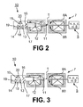
- FIG. 2 shows a detail of the apparatus according to the invention.
- Figure 2 shows the particle-optical objective lens 7, showing the two pole face 8A, 8B.
- the sample manipulator 5, here shown capable of positioning the sample 1 with 5 degrees of freedom, is connected with the sample 1.
- the sample faces the optical microscope 10 .
- the optical microscope comprises a laser unit 19, producing a beam of light.
- This beam of light is parallelized with lens 14, then passes through a beam splitter 18, and then impinges on mirrors 17 and 16.
- These mirrors are mounted on actuators, e.g. piezo actuators, and can thereby change the direction of the beam.
- the beam is then imaged with two lenses 12, 11 onto the sample.
- Lens 12 images the rotational plane of the mirrors 16, 17 in the vicinity of lens 11.
- the beam is imaged in such a way that tilting of the beam in lens 11 occurs with a minimal displacement of the beam in that lens.
- the field of view of the optical microscope is large compared to an optical microscope without such a lens.
- Light emanating from the sample is gathered by lens 11, and follows the way back until it comes to the beam splitter 18.
- the detected light is then deflected to a photonic detector 20.
- a lens 15 may help focussing the light on the detector.
- the detector may be a single photon detector, or a more conventional detector, depending on the sensitivity needed.
- the aberration coefficients of all optical elements can be optimized for the wave length of that light.
- the chromatic error of the lenses do not affect the image quality.
- Monochromatic light must in this context be interpreted as light showing sufficient small spread in wavelength so as to avoid the formation of a focus with a diameter that is dominated by chromatic aberration(s).
- the light coming from the sample travelling to the detector may be of a different colour (e.g. because fluorescent light is detected), but as mentioned earlier lens aberrations occurring in the imaging path do not affect the image quality/resolution.
- illumination optics may be constructed that are compensated for chromatic aberrations on two or more wavelengths and still show diameters of those lens elements that are placed between the pole faces that are sufficiently small.
- coatings, reflection of the beam splitter and such may need to be optimized for the wave length of the detected light as well.
- the optical microscope shown here is drawn very schematic, and that many differences may occur. It is e.g. possible to insert an optical fibre between lens 13 and mirror 17, thereby enabling the laser and detector to be placed away from the column of the apparatus.
- the beam splitter may also be a grating, and lenses may be added or eliminated according to the exact implementation of the optical microscope. Also e.g.
- a beam polarizer may be incorporated into the optical microscope. It is also remarked that, as no absolute monochromaticity of the illuminating beam is required, but only such monochromaticity so as to form a focus that is not dominated by chromatic aberration, also light filtered with a colour filter from e.g. a device emitting white light can be used.
- Figure 3 shows a detail of the apparatus according to the invention, where the optical microscope is retracted.
- Figure 3 can be thought to be derived from figure 2 .
- the optical microscope 10 is slightly retracted, thereby freeing the space around the first sample position.
- the sample 1 can be positioned freely between the pole pieces 8A, 8B without contacting the optical microscope.
- the retraction may also enable other parts of the apparatus, such as e.g. X-ray detectors, secondary electron detectors, etc., to be positioned near the sample.
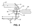
- Figure 4 shows a detail of the apparatus according to the invention, where the sample is illuminated at one side and observed at the other side.
- Figure 4 shows an incoming beam of light round optical axis 27, which is deflected by mirror 21 towards the sample 1.
- a lens 23 focuses the light onto the sample.
- the sample is mounted on a TEM grid 25, which is held in place on the distal end 5A of the sample manipulator with a circular spring 26.
- Light emitted by the sample or transmitted through the sample, depicted by rays 28, is gathered by lens 24 and deflected by mirror 22 in a direction parallel to the incoming beam of light.
- the particle-optical axis is e.g. perpendicular to the plane of the figure.
- the beam of light may be scanned over the sample with other mirrors, but that it can also be envisaged that mirror 21 is used for the scanning. In that case the mirror 21 must by actuated by actuators. It is also remarked that, instead of guiding the light to and from the sample with mirrors (21, 22), e.g. optical fibres may be used.
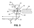
- Figure 5 depicts a detail of the apparatus according to the invention, equipped with a SNOM.
- Figure 5 can be thought to be derived from figure 4 .
- the sample is illuminated with the probe 32 of a SNOM unit 33.
- the SNOM unit comprises a mechanical platform 31 on which the probe is mounted, said platform mechanically scanning the probe over the surface of the sample. To that end the platform can be actuated with e.g. piezo-electric actuators (not shown).
- the probe is e.g. a tapering metalised glass fibre, with an aperture near the sample. The aperture has a diameter of e.g. 20 to 50 nm, but smaller and larger diameters may be used. Light coming from fibre 30 is fed into the probe.
- each of the embodiments described before can be realized with cooling surfaces and cooling conduits so that the sample can be kept at a cryogenic temperature.
- Such measures are well known from conventional cryo-TEM's.
Landscapes
- Chemical & Material Sciences (AREA)
- Analytical Chemistry (AREA)
- Health & Medical Sciences (AREA)
- Nuclear Medicine, Radiotherapy & Molecular Imaging (AREA)
- Physics & Mathematics (AREA)
- Life Sciences & Earth Sciences (AREA)
- Biochemistry (AREA)
- General Health & Medical Sciences (AREA)
- General Physics & Mathematics (AREA)
- Immunology (AREA)
- Pathology (AREA)
- Microscoopes, Condenser (AREA)
- Investigating Or Analysing Materials By Optical Means (AREA)
Abstract
The invention relates to an apparatus for observing a sample (1) with a TEM column and a high resolution optical microscope (10). The sample position for observing the sample with the TEM column is close to the sample position for observing the sample with the optical microscope. By using an optical microscope of the scanning type, and preferably using monochromatic light, the lens elements of the optical microscope facing the sample position can be sufficiently small to be positioned between the pole faces (8A,8B) of the (magnetic) particle-optical objective lens. This is in contrast with the objective lens systems conventionally used in optical microscopes, which show a large diameter.
Description
- The invention relates to a particle-optical apparatus for observing a thin sample, the apparatus comprising:
- a particle source for producing a beam of particles along a particle-optical axis,
- particle-optical lenses arranged round the particle-optical axis for manipulating said beam of particles,
- a sample manipulator for positioning the sample on a first sample position, the first sample position located on the particle-optical axis and between two pole faces of a particle-optical lens, the so-named particle-optical objective lens,
- detection means for detecting particles transmitted through the sample, and
- an optical microscope to observe the sample at a second sample position.
- Such an apparatus was sold by Akashi Seisakusho Ltd, Japan, under the name LEM-2000.
- The known apparatus comprises a Transmission Electron Microscope column (TEM column) and an optical microscope. It is equipped to observe samples mounted on large 7 mm grids with the light microscope or in the TEM column.
The optical microscope is mounted at the front side of the apparatus -that is: the side where the operator resides-. The optical microscope has a binocular and the operator observes a sample that is mounted vertically (the optical path is bent by a prism over 90 degrees). The magnification of the optical microscope is between 50x and 250x. A condenser illuminates the sample through the grid. The sample resides in atmosphere when observed with the optical microscope. Behind the optical microscope a TEM column is mounted in horizontal position.
The TEM operates with an electron energy of up to 100 keV and uses 6 electron optical lenses. Transmitted electrons are imaged on a fluorescent screen with a magnification of between 250x and 45000x. The fluorescent screen can be observed with binoculars, or the screen can be temporarily exchanged for a film cassette to make photos.
The TEM column comprises a sample chamber in which the sample must be placed for observation. The sample chamber is evacuated when observing the sample in the TEM.
A shuttle mechanism transports the sample from the first position where it is observed with the optical microscope to the second position where it is observed in the TEM. To that end the sample is transferred through an airlock. - A disadvantage of the known apparatus is that the sample must be transferred between two observation positions: one for the optical microscope located in air and another for the TEM located in a vacuum environment. Therefore the sample must pass through an airlock when travelling between the two observation positions. This results in relative large positional inaccuracies when the sample is placed in the TEM, resulting in long delays to determine the exact position. Especially for modern types of TEM's with resolutions down to 0.1 nm or better, the mapping of the optical microscope image to the TEM image will be very time consuming. When a sample has to be observed repeatedly with the optical microscope and the TEM, the sample must be positioned accurately in the TEM column repeatedly, resulting in long delay times.
- Another disadvantage is that the sample must pass through an airlock between the optical microscope and the TEM. As a result of this a delay due to pump down or due to venting occurs when the sample is travelling through the airlock. When a sample has to be observed repeatedly with the optical microscope and the TEM, the sample must pass through the airlock repeatedly, and must be positioned accurately in the TEM column, resulting in long delay times.
- A further disadvantage is that the sample is in atmosphere when observed with the optical microscope, and in vacuum when observed in the TEM. This can result in warping of the sample, as well as in changes in the sample due to boiling, outgassing, etc. Comparison and/or mapping of images obtained by the two techniques (particle-optical inspection and inspection with an optical microscope) may be hampered by this. Also, when the sample is passed through the airlock repeatedly because it must be observed by the optical microscope and the TEM repeatedly, the repeated evacuating the sample and exposing it to air again can cause the sample to change after each evacuation/venting cycle. This may result in poor comparison/mapping of the sample even in subsequent vented and/or evacuated situation.
- The invention aims to provide an apparatus overcoming said disadvantages.
- To that end the apparatus according to the invention is characterized in that
- the second sample position is located on or near the particle-optical axis and between the two pole faces of the particle-optical objective lens, and
- the optical microscope is equipped to illuminate the sample with a point of light, said point of light being scanned over the sample.
- By locating the second sample position on or near the particle-optical axis and between the pole faces, the first and the second sample position are very close together. This makes it possible to use the sample manipulator used for positioning the sample at the first sample position to position the sample at the second sample position as well. As known to the person skilled in the art of sample manipulators for particle-optical apparatus, such as a TEM, such sample manipulators often show a positional reproducibility and accuracy of better than 200 nm and 0.1 degrees, with step sizes even smaller. It is remarked that such sample manipulators are often capable to position a sample with e.g. 5 degrees of freedom, e.g. along 3 translation axis and round 2 rotational axis. Due to the small distance between the two sample positions the sample manipulator used in the particle-optical column, with its high accuracy and reproducibility, can be used to position the sample in both the first and the second sample position. The resultant high positional accuracy enables easy mapping of the optical microscope's image to the TEM image.
- The second sample position is in the same (vacuum) environment as the first sample position. Therefore the sample need only be evacuated once, even when repeatedly observed with the optical microscope and the TEM. Therefore delay to repeated pumping and venting is eliminated.
- As the sample is kept in the same vacuum environment during observation in the first sample position or the second sample position, no deformation and/or warping will occur due to repeated exposure to vacuum or air.
- By equipping the optical microscope such that the sample is scanned with a point of light, the resolution obtained with the light microscope is not limited by the aberrations occurring in the detection path, but only in the illumination path, in which the diameter of the point of light generated. Such a method in which the sample is scanned with a point of light is known from e.g. scanning optical microscopy, where the sample is illuminated with a small focus that is scanned over the surface of the sample. Another such method is known from Scanning Near-field Optical Microscopy (SNOM), where a point of light is emanating from a small probe. This enables the use of optical lens systems with a much smaller diameter than the diameter of conventional optical objective lens systems. The reason for this is as follows:
- It could be envisaged to place a conventional optical objective lens system between the pole faces of the particle-optical lens. High-resolution optical objective lens systems have high numerical apertures and short working distances of e.g. 1 mm or less. Therefore the optical objective lens system needs to be placed close to the second sample position, and the diameter of the optical element facing the sample needs to be large (due to the required high numerical aperture normally equal to or larger than the working distance). Such objectives need to be corrected for aberrations. As known to the person skilled in the art of optical microscopy this leads to an objective lens system comprising several closely spaced optical elements, with certain of these elements having a diameter much larger than the lens closest to the sample. Therefore high-resolution objectives have a diameter too large to fit between the pole faces. Also their construction, in which optical elements are kitted together, is often incompatible with the vacuum of the sample position, typically 10-6 mbar or less.
- Contrary to this the objective used in e.g. scanning optical microscopy need not be compensated for aberrations in the detecting path, as these do not affect the image quality. This is due to the fact that, at a certain moment in time, all light emanating from the sample emanates from one point only: the point where the beam impinges on the sample. The spatial resolution is thus a direct result of the diameter of the point that is formed on the sample, and is not influenced by lens aberrations in the detection path. As a result the optical objective lens can be of simple construction, e.g. an aspherical singlet. Such a singlet can have a much reduced outer diameter when compared to a conventional microscope objective with similar resolution and working distance.
- The point of light can be scanned over the sample by e.g. one or two movable mirrors in the illuminating optical path. By tilting the one or more mirrors with e.g. piezo actuators or using electric coils and a magnet, the beam is deflected, resulting in a different position where the beam impinges on the sample.
- An additional advantage of scanning the beam of light over the sample is that the magnification of the image is simply changed by changing the scan amplitude. Changing the scan amplitude is done by changing the amplitude of the actuators moving the mirror(s), e.g. by changing an electric signal. This eliminates the need to change the objective lens system, which is normally done when using conventional optical objective lens systems. It is remarked that, as the objective lens system is placed in a vacuum environment and the space around the objective lens system is limited, changing of the objective lens system would be more difficult than in a conventional optical microscope
- In an embodiment of the apparatus according to the invention the point of light is generated by focusing a beam of light.
- In this embodiment a beam of light, e.g. the beam coming from e.g. a laser device, a LED or semiconductor laser, or a lamp, is focused onto the sample.
- It is remarked that the lens focusing the beam on the sample must form a fine focus on the sample. Lens aberrations that do not influence the diameter of the focus, such as field curvature, can be ignored, or e.g. corrected for in the scan system. If the illuminating beam is sufficiently monochromatic, chromatic aberration of the lens does not influence the diameter of the focus either, and thus does not deteriorate the resolution, even when the light that is detected is of a different colour than the light illuminating the sample. The latter occurs when detecting e.g. luminescence (fluorescence and/or phosphorescence) of the sample, and in e.g. Fluorescent Resonant Energy Transfer (FRET) and Fluorescent Lifetime IMaging (FLIM) techniques.
- In another embodiment of the apparatus according to the invention the point of light is generated by the probe of a Scanning Near-field Optical Microscope (SNOM).
- In a SNOM light is emitted by a metal coated glass fibre (or at least a fibre of a material transparent to light) with a sub-micron aperture, the aperture showing a diameter of typically between 20-50 nm. The aperture can be smaller than the wavelength of the light emitted by the probe. The aperture is positioned close to the surface of the sample. By scanning the probe over the surface, a point of light is scanned over the sample.
It is remarked that it could be envisaged that instead of a metal coated glass fibre a hollow cone is used from which the light emerges. - In a further embodiment the point of light is formed from monochrome light.
- In this embodiment the illuminating optical path uses only one colour, and thus chromatic aberration is of no consequence in the illuminating path either. Therefore no correction for chromatic aberration is needed in either the illuminating optics or the imaging optics (used in the detection path).
- In another embodiment of the apparatus according to the invention the optical microscope is equipped with a lens for gathering light originating from the second sample position, said lens having a light-optical axis, and the apparatus is equipped to position the sample in such a way that the surface of the sample is substantially perpendicular to the optical axis when observing the sample with the optical microscope.
- In a further embodiment of the apparatus according to the invention the light-optical axis is substantially perpendicular to the particle-optical axis.
- The space between the pole pieces of the objective lens is rather limited. The easiest access to the second sample position (between the pole faces and near the particle-optical axis) is by inserting the optical microscope perpendicular to the particle-optical axis.
- In another embodiment of the apparatus according to the invention the optical microscope is equipped with an optical lens, said optical lens positioned closest to the second sample position when imaging the second sample position, and at least said optical lens retractably mounted with respect to the particle-optical axis.
- By making at least this lens (and its mounting) retractable, more space becomes available round the particle-optical axis when the sample is not observed with the light microscope. This is advantageous as the first and the second sample position are so close together and enables other parts of the apparatus, such as X-ray detectors, secondary electron detectors, etc., to be positioned close to the first sample position.
- In yet another embodiment of the apparatus according to the invention at least part of the sample manipulator and the vicinity of the first and the second sample position are equipped to be cooled to a cryogenic temperature, thereby enabling observation of cryogenically cooled samples.
- Particle-optical apparatus where a cryogenically cooled sample may be observed, such as a cryo-TEM, are known per se. An example is the Tecnai G2 Polara, commercially available from FEI Company, Hillsboro (OR), USA. In such instruments the sample manipulator and the vicinity of the sample position are cooled to cryogenic temperatures, e.g. the temperature of boiling nitrogen or boiling helium. By cooling the vicinity of the second sample position likewise, a cryogenically cooled sample can be observed with both the particle beam and the optical microscope.
- In still another embodiment of the apparatus according to the invention the apparatus is equipped to illuminate the sample at one site and to detect light from the other side of the thin sample.
- In this embodiment the light transmitted through the sample is observed.
- In yet still another embodiment according to the invention the sample is positioned in the first and in the second sample position with one sample manipulator.
- Using the same manipulator for both sample positions results in a simpler design then when two separate manipulators, and a transfer mechanism to transfer the sample from one manipulator to the other, would be used.
- In an aspect of the invention, a method for analysing a sample, said method comprising providing an apparatus equipped with a particle microscope and a optical microscope, said apparatus equipped with a particle-optical lens with two pole faces, said lens showing a particle-optical axis, said particle microscope showing a first sample position located between said pole faces and located at the particle-optical axis, providing a thin sample to be analysed in the apparatus, positioning the sample at the first sample position, imaging the sample positioned at the first sample position with the particle microscope, positioning the sample in a second sample position where the sample can be imaged by the optical microscope and imaging the sample with the optical microscope,
is characterized in that
the second sample position is located between said two pole faces of the particle-optical lens, and the optical microscope employs a scanned point of light to illuminate the sample. - It is remarked that, although in the above it is first recited that the sample is first imaged in the first sample position and then it is recited that the sample is positioned in the second sample position, this does not imply a necessary sequence of steps. It is well possible to do these steps in the other order, or repeatedly perform the steps in an arbitrary order.
- In an embodiment of the method according to the invention the sample is positioned in the first and in the second sample position positioned with one sample manipulator.
- In another embodiment of the method according to the invention the sample in the second sample position is oriented substantially perpendicular to the particle-optical axis.
- The invention is now further elucidated on the basis of schematic drawings, in which corresponding features are identified by identical numerals. To this end:
-
figure 1 shows an apparatus according to the invention, -
figure 2 shows a detail of the apparatus according to the invention, -
figure 3 shows a detail of the apparatus according to the invention, where the optical microscope is retracted, -
figure 4 shows a detail of the apparatus according to the invention, where the sample is illuminated at one side and observed at the other side, -
figure 5 shows a detail of the apparatus according to the invention, in which the apparatus is equipped with a SNOM. -
Figure 1 shows avacuum chamber 6 in which aparticle source 2 is located. The particle source generates a beam of particles, e.g. in the form of an electron beam in which the electrons have an energy of e.g. 300 keV, along particle-optical axis 3. The electron beam is manipulated (focused) by particle-optical lenses
Sample manipulator 5 is used to position asample 1 onto the first sample position, where the beam of particles impinges on the sample. The first sample position is located between the pole faces 8A, 8B of the particle-opticalobjective lens 7.
The part of the electron beam transmitted through the sample is imaged by the particle-optical lenses
Anoptical microscope 10 enables observation of the sample when it is in the second sample position. - As mentioned earlier the sample is normally a flat, very thin sample. For high resolution images the sample is often less than 100 nm thick, preferably even less than 50 nm thick. Such a sample is very fragile and therefore it is supported on a grid, e.g. a copper grid, said grid mounted on the
sample manipulator 5. Such grids are known to the person skilled in the art as TEM grids.
To observe an area of interest of the sample with the particle beam the area of interest is brought on the particle-optical axis with thesample manipulator 5. While observing the sample with the particle beam, the orientation of the sample can be perpendicular to the particle-optical axis, but for certain techniques, such as 3D tomography, the sample may also be tilted with respect to the particle-optical axis.
To enable positioning the sample to meet these demands, the sample manipulator is able to position the sample with e.g. 3 translational and 2 rotational degrees of freedom, although also sample manipulators with less or even more degrees of freedom are known.
All sample positions/orientations that may be used to image the sample with the particle beam are referred to as the first sample position. - The
optical microscope 10 observes a position between the pole faces 8A, 8B. To form the best image with the optical microscope the sample need to be tilted to a position substantially perpendicular to the optical axis of the optical microscope. This position/orientation is the second sample position. - The optical microscope, or at least that part of the optical microscope closest to the particle-optical axis, is retractably mounted, and can be retracted to offer more space round the sample when the sample is not observed with the optical microscope. This additional space may be needed to offer access to the sample by e.g. other types of detectors, such as the commonly known secondary electron detectors, X-ray detectors, etc. that may be used to gather information about the sample when the sample is irradiated with the electron beam.
- It is remarked that in this
figure sample manipulator 5 andoptical microscope 10 are depicted as sharing a plane perpendicular to the particle-optical axis 3 and are positioned opposite to each other. This is not necessary, and also embodiments where the manipulator and optical microscope are in a plane but spaced e.g. 90 degrees or 120 degrees apart, are possible. It is also possible that one or both elements show a symmetry axis that is not perpendicular to the particle-optical axis. -
Figure 2 shows a detail of the apparatus according to the invention. -
Figure 2 shows the particle-opticalobjective lens 7, showing the twopole face sample manipulator 5, here shown capable of positioning thesample 1 with 5 degrees of freedom, is connected with the sample 1.The sample faces theoptical microscope 10. - The optical microscope comprises a
laser unit 19, producing a beam of light. This beam of light is parallelized withlens 14, then passes through abeam splitter 18, and then impinges onmirrors lenses
Lens 12 images the rotational plane of themirrors lens 11. In other words: the beam is imaged in such a way that tilting of the beam inlens 11 occurs with a minimal displacement of the beam in that lens. As a result the field of view of the optical microscope is large compared to an optical microscope without such a lens.
Light emanating from the sample, such as reflected light or fluorescent light, is gathered bylens 11, and follows the way back until it comes to thebeam splitter 18. The detected light is then deflected to aphotonic detector 20. Alens 15 may help focussing the light on the detector. The detector may be a single photon detector, or a more conventional detector, depending on the sensitivity needed. - As the
laser 19 produces a monochromatic beam of light, the aberration coefficients of all optical elements can be optimized for the wave length of that light. The chromatic error of the lenses do not affect the image quality. Monochromatic light must in this context be interpreted as light showing sufficient small spread in wavelength so as to avoid the formation of a focus with a diameter that is dominated by chromatic aberration(s). The light coming from the sample travelling to the detector may be of a different colour (e.g. because fluorescent light is detected), but as mentioned earlier lens aberrations occurring in the imaging path do not affect the image quality/resolution. - It is remarked that also illumination optics may be constructed that are compensated for chromatic aberrations on two or more wavelengths and still show diameters of those lens elements that are placed between the pole faces that are sufficiently small.
It is to be mentioned that coatings, reflection of the beam splitter and such may need to be optimized for the wave length of the detected light as well.
It is further mentioned that the optical microscope shown here is drawn very schematic, and that many differences may occur. It is e.g. possible to insert an optical fibre betweenlens 13 andmirror 17, thereby enabling the laser and detector to be placed away from the column of the apparatus. The beam splitter may also be a grating, and lenses may be added or eliminated according to the exact implementation of the optical microscope. Also e.g. a beam polarizer may be incorporated into the optical microscope.
It is also remarked that, as no absolute monochromaticity of the illuminating beam is required, but only such monochromaticity so as to form a focus that is not dominated by chromatic aberration, also light filtered with a colour filter from e.g. a device emitting white light can be used. -
Figure 3 shows a detail of the apparatus according to the invention, where the optical microscope is retracted. -
Figure 3 can be thought to be derived fromfigure 2 . As can be seen, theoptical microscope 10 is slightly retracted, thereby freeing the space around the first sample position. Hereby thesample 1 can be positioned freely between thepole pieces - It is remarked that in this figure it is shown that the whole
optical microscope 10 is retracted. It will be recognized by the person skilled in the art that it is sufficient when only part of the optical microscope, the part comprising thelens 11 and its mounting, is retracted. -
Figure 4 shows a detail of the apparatus according to the invention, where the sample is illuminated at one side and observed at the other side. -
Figure 4 shows an incoming beam of light roundoptical axis 27, which is deflected bymirror 21 towards thesample 1. Alens 23 focuses the light onto the sample. The sample is mounted on aTEM grid 25, which is held in place on thedistal end 5A of the sample manipulator with acircular spring 26. Light emitted by the sample or transmitted through the sample, depicted byrays 28, is gathered bylens 24 and deflected bymirror 22 in a direction parallel to the incoming beam of light. The particle-optical axis is e.g. perpendicular to the plane of the figure. - It is remarked that the beam of light may be scanned over the sample with other mirrors, but that it can also be envisaged that
mirror 21 is used for the scanning. In that case themirror 21 must by actuated by actuators.
It is also remarked that, instead of guiding the light to and from the sample with mirrors (21, 22), e.g. optical fibres may be used. -
Figure 5 depicts a detail of the apparatus according to the invention, equipped with a SNOM. -
Figure 5 can be thought to be derived fromfigure 4 . Instead of illuminating the sample with a focused beam of light, the sample is illuminated with theprobe 32 of aSNOM unit 33. The SNOM unit comprises amechanical platform 31 on which the probe is mounted, said platform mechanically scanning the probe over the surface of the sample. To that end the platform can be actuated with e.g. piezo-electric actuators (not shown). The probe is e.g. a tapering metalised glass fibre, with an aperture near the sample. The aperture has a diameter of e.g. 20 to 50 nm, but smaller and larger diameters may be used. Light coming fromfibre 30 is fed into the probe. - As known to the person skilled in the art of Scanning Near-field Optical Microscopy, light can escape through such a small aperture, even when the aperture is smaller than the wavelength of the light escaping from it. This enables an optical resolution well below the resolution that can be obtained by focusing a beam of light on the sample.
- It is remarked that each of the embodiments described before can be realized with cooling surfaces and cooling conduits so that the sample can be kept at a cryogenic temperature. Such measures are well known from conventional cryo-TEM's.
Claims (14)
- Particle-optical apparatus for observing a thin sample (1), the apparatus comprising:• a particle source (2) for producing a beam of particles along a particle-optical axis (3),• particle-optical lenses (4A, 4B, 4C, 4D) arranged round the particle-optical axis for manipulating said beam of particles,• a sample manipulator (5) for positioning the sample on a first sample position, the first sample position located on the particle-optical axis and between two pole faces (8A, 8B) of a particle-optical lens, the so-named particle-optical objective lens (7),• detection means (9) for detecting particles transmitted through the sample, and• an optical microscope (10) to observe the sample at a second sample position,characterized in that• the second sample position is located on or near the particle-optical axis and between the two pole faces (8A, 8B) of the particle-optical objective lens, and• the optical microscope is equipped to illuminate the sample with a point of light, said point of light being scanned over the sample.
- The particle-optical apparatus according to claim 1, in which the point of light is generated by focusing a beam of light.
- The particle-optical apparatus according to claim 1, in which the point of light is generated by a Scanning Near-field Optical Microscope (SNOM) probe, said SNOM probe being scanned over the surface of the sample.
- The particle-optical apparatus according to claim 2 or claim 3, in which the point of light is formed from monochrome light.
- The particle-optical apparatus according to any of the preceding claims, in which the optical microscope is equipped with a lens (11) for gathering light originating from the second sample position, said lens having a light-optical axis, and the apparatus is equipped to position the sample (1) in such a way that the surface of the sample is substantially perpendicular to the optical axis when observing the sample with the optical microscope (10).
- The particle-optical apparatus according to claim 5 in which the light-optical axis is substantially perpendicular to the particle-optical axis (3).
- The particle-optical apparatus according to any of the preceding claims in which the optical microscope (10) is equipped with an optical lens (11), said optical lens positioned closest to the first sample position when imaging the first sample position, and at least said optical lens retractably mounted with respect to the particle-optical axis.
- The particle-optical apparatus according to any of the preceding claims in which at least part of the sample manipulator (5) and the vicinity of the first and the second sample position are equipped to be cooled to a cryogenic temperature, thereby enabling observation of cryogenically cooled samples.
- The particle-optical apparatus according to any of the preceding claims in which the apparatus is equipped to illuminate the sample at one site and to detect light from the other side of the thin sample.
- The particle-optical apparatus according to any of the preceding claims in which the sample is positioned in the first and in the second sample position with one sample manipulator.
- Kit for upgrading a conventional particle-optical apparatus to a particle-optical apparatus according to any of the preceding claims
- Method for analysing a sample, the method comprising:• providing an apparatus equipped with a particle microscope and a optical microscope, said apparatus equipped with a particle-optical lens with two pole faces, said lens showing a particle-optical axis, said particle microscope showing a first sample position located between said pole faces and located at the particle-optical axis,• providing a thin sample (1) to be analysed in the apparatus,• positioning the sample at the first sample position,• imaging the sample positioned at the first sample position with the particle microscope,• positioning the sample at a second sample position where the sample may be imaged by the optical microscope and• imaging the sample with the optical microscope,characterized in that• the second sample position is located between said two pole faces (8A, 8B) of the particle-optical lens (7),• the optical microscope (10) employs a scanned point of light to illuminate the sample.
- The method according to claim 12 in which the first sample position and the second sample position intersect each other
- The method according to claim 12 or claim 13 in which the sample in the second sample position is oriented substantially perpendicular to the particle-optical axis.
Priority Applications (5)
| Application Number | Priority Date | Filing Date | Title |
|---|---|---|---|
| EP07101725A EP1953791A1 (en) | 2007-02-05 | 2007-02-05 | Apparatus for observing a sample with a particle beam and an optical microscope |
| CN2008100740369A CN101241087B (en) | 2007-02-05 | 2008-02-01 | Apparatus for observing a sample with a particle beam and an optical microscope |
| EP08150931A EP1953792B1 (en) | 2007-02-05 | 2008-02-01 | Apparatus for observing a sample with a particle beam and an optical microscope |
| JP2008023533A JP5534646B2 (en) | 2007-02-05 | 2008-02-04 | Apparatus for observing a sample with a microscope using a particle beam and light |
| US12/026,419 US7671333B2 (en) | 2007-02-05 | 2008-02-05 | Apparatus for observing a sample with a particle beam and an optical microscope |
Applications Claiming Priority (1)
| Application Number | Priority Date | Filing Date | Title |
|---|---|---|---|
| EP07101725A EP1953791A1 (en) | 2007-02-05 | 2007-02-05 | Apparatus for observing a sample with a particle beam and an optical microscope |
Publications (1)
| Publication Number | Publication Date |
|---|---|
| EP1953791A1 true EP1953791A1 (en) | 2008-08-06 |
Family
ID=38255373
Family Applications (2)
| Application Number | Title | Priority Date | Filing Date |
|---|---|---|---|
| EP07101725A Withdrawn EP1953791A1 (en) | 2007-02-05 | 2007-02-05 | Apparatus for observing a sample with a particle beam and an optical microscope |
| EP08150931A Active EP1953792B1 (en) | 2007-02-05 | 2008-02-01 | Apparatus for observing a sample with a particle beam and an optical microscope |
Family Applications After (1)
| Application Number | Title | Priority Date | Filing Date |
|---|---|---|---|
| EP08150931A Active EP1953792B1 (en) | 2007-02-05 | 2008-02-01 | Apparatus for observing a sample with a particle beam and an optical microscope |
Country Status (4)
| Country | Link |
|---|---|
| US (1) | US7671333B2 (en) |
| EP (2) | EP1953791A1 (en) |
| JP (1) | JP5534646B2 (en) |
| CN (1) | CN101241087B (en) |
Cited By (6)
| Publication number | Priority date | Publication date | Assignee | Title |
|---|---|---|---|---|
| DE102009015341A1 (en) * | 2009-03-27 | 2010-10-07 | Carl Zeiss Ag | Method for optical testing of sample during e.g. chemical analysis, involves detecting optical emission of sample depending on characteristic modulation i.e. temporally periodic modulation, of particle beam |
| WO2010120238A1 (en) | 2009-04-15 | 2010-10-21 | Nanofactory Instruments Ab | Optical probing in electron microscopes |
| WO2011146084A1 (en) * | 2010-05-20 | 2011-11-24 | California Institute Of Technology | Method and system for 4d tomography and ultrafast scanning electron microscopy |
| EP2469253A1 (en) * | 2010-12-24 | 2012-06-27 | HybriScan Technologies Holding BV | System for electron microscopy and Raman spectroscopy |
| NL1040008C2 (en) * | 2013-01-18 | 2014-07-21 | Univ Delft Tech | Optical and integrated inspection apparatus and method. |
| US9310596B2 (en) | 2010-04-06 | 2016-04-12 | Inter-University Research Institute Corporation National Institute Of Natural Sciences | Compound microscope device |
Families Citing this family (18)
| Publication number | Priority date | Publication date | Assignee | Title |
|---|---|---|---|---|
| GB0901040D0 (en) * | 2009-01-22 | 2009-03-11 | Renishaw Plc | Optical measuring method and system |
| EP2576759A4 (en) * | 2010-05-25 | 2014-01-22 | Arryx Inc | Methods and apparatuses for detection of positional freedom of particles in biological and chemical analyses and applications in immunodiagnostics |
| EP2601477B1 (en) | 2010-08-02 | 2021-09-22 | Oxford Instruments America, Inc. | Method for acquiring simultaneous and overlapping optical and charged particle beam images |
| JP5699023B2 (en) | 2011-04-11 | 2015-04-08 | 株式会社日立ハイテクノロジーズ | Charged particle beam equipment |
| CN106158567B (en) * | 2012-03-16 | 2017-12-15 | 株式会社日立高新技术 | Charged particle bundle device, sample observing system |
| EP2757402B1 (en) * | 2013-01-22 | 2016-03-30 | FEI Company | Method of observing samples with a fluorescent microscope |
| US9564291B1 (en) * | 2014-01-27 | 2017-02-07 | Mochii, Inc. | Hybrid charged-particle beam and light beam microscopy |
| EP2899743B1 (en) | 2014-01-27 | 2016-09-21 | Fei Company | Correlative optical and charged particle microscope |
| CN104142302B (en) | 2014-07-28 | 2017-02-15 | 中国科学院生物物理研究所 | Optical vacuum cold station for light microscope and electron microscope correlated imaging |
| CN104502315A (en) * | 2014-12-02 | 2015-04-08 | 中国科学院半导体研究所 | Micro-region fluorescent scanning measurement system |
| EP3038131A1 (en) | 2014-12-22 | 2016-06-29 | FEI Company | Improved specimen holder for a charged particle microscope |
| KR101725137B1 (en) * | 2015-08-21 | 2017-04-26 | 한국표준과학연구원 | Sample chamber for electron microscope and the electron microscope including the same |
| CN106525845B (en) | 2016-10-11 | 2023-11-03 | 聚束科技(北京)有限公司 | A charged particle beam system, photoelectric joint detection system and method |
| CN106645250B (en) * | 2016-11-21 | 2024-04-26 | 宁波聚瑞精密仪器有限公司 | Scanning transmission electron microscope with optical imaging function |
| US10176963B2 (en) | 2016-12-09 | 2019-01-08 | Waviks, Inc. | Method and apparatus for alignment of optical and charged-particle beams in an electron microscope |
| US11536659B2 (en) * | 2016-12-27 | 2022-12-27 | The Regents Of The University Of Michigan | Laser emission based microscope |
| CN109683301A (en) * | 2019-02-01 | 2019-04-26 | 宁波永新光学股份有限公司 | One kind just setting microscopical lighting device |
| US11551906B1 (en) * | 2021-06-30 | 2023-01-10 | Fei Company | Time-gated detection, dual-layer SPAD-based electron detection |
Citations (6)
| Publication number | Priority date | Publication date | Assignee | Title |
|---|---|---|---|---|
| GB2059120A (en) * | 1979-09-05 | 1981-04-15 | Philips Nv | Automatic beam correction in a scanning transmission electron microscope |
| FR2596863A1 (en) * | 1986-04-07 | 1987-10-09 | Centre Nat Rech Scient | Analytic microscopy device, capable of forming both a Raman probe and an electronic probe |
| US5811804A (en) * | 1994-01-24 | 1998-09-22 | Biomaterials Research Group Stichting Azl | Electron microscope with raman spectroscopy |
| WO1999058939A1 (en) * | 1998-05-09 | 1999-11-18 | Renishaw Plc | Electron microscope and spectroscopy system |
| US20040090621A1 (en) * | 2001-03-15 | 2004-05-13 | Robert Bennett | Spectroscopy apparatus and method |
| WO2005098895A2 (en) * | 2004-04-02 | 2005-10-20 | California Institute Of Technology | Method and system for ultrafast photoelectron microscope |
Family Cites Families (23)
| Publication number | Priority date | Publication date | Assignee | Title |
|---|---|---|---|---|
| US3740147A (en) | 1972-01-10 | 1973-06-19 | Farrand Optical Co Inc | Microspectrophotometer with two fields of view |
| JPS51142343A (en) * | 1975-05-23 | 1976-12-07 | Hitachi Ltd | On-off device for optical microscope |
| FR2498767A1 (en) | 1981-01-23 | 1982-07-30 | Cameca | MICRO-ANALYZER WITH ELECTRONIC PROBE COMPRISING A DOUBLE-GROWING OBSERVATION SYSTEM |
| JPS61104551A (en) * | 1984-10-29 | 1986-05-22 | Hitachi Ltd | electronic microscope |
| US4897545A (en) * | 1987-05-21 | 1990-01-30 | Electroscan Corporation | Electron detector for use in a gaseous environment |
| JP2578519B2 (en) | 1990-06-01 | 1997-02-05 | 株式会社日立製作所 | Charged particle beam exposure system with position detection function by light beam |
| JPH0471152A (en) * | 1990-07-11 | 1992-03-05 | Nec Kyushu Ltd | Scanning type electron microscope |
| JPH09203864A (en) | 1996-01-25 | 1997-08-05 | Nikon Corp | NFM integrated microscope |
| US5905266A (en) | 1996-12-19 | 1999-05-18 | Schlumberger Technologies, Inc. | Charged particle beam system with optical microscope |
| GB0118981D0 (en) * | 2001-08-03 | 2001-09-26 | Renishaw Plc | Electron microscope and spectroscopy system |
| JP3035612B1 (en) * | 1999-01-07 | 2000-04-24 | 大阪大学長 | Scanning microscope equipment |
| JP2000208083A (en) * | 1999-01-20 | 2000-07-28 | Jeol Ltd | Electron microscope sample cooling device |
| JP2000251819A (en) * | 1999-03-04 | 2000-09-14 | Hitachi Ltd | Sample cooling holder |
| US6373070B1 (en) | 1999-10-12 | 2002-04-16 | Fei Company | Method apparatus for a coaxial optical microscope with focused ion beam |
| JP4200665B2 (en) * | 2001-05-08 | 2008-12-24 | 株式会社日立製作所 | Processing equipment |
| JP2003121748A (en) * | 2001-10-16 | 2003-04-23 | Koike Seiki Kk | Color laser scanning microscope |
| JP2003263969A (en) * | 2002-03-08 | 2003-09-19 | Jeol Ltd | Sample holder |
| JP2003282016A (en) * | 2002-03-26 | 2003-10-03 | Seiko Instruments Inc | Sample stage tilt mechanism for charged particle microscope with peripheral equipment |
| JP4636897B2 (en) * | 2005-02-18 | 2011-02-23 | 株式会社日立ハイテクサイエンスシステムズ | Scanning electron microscope |
| GB2428868B (en) * | 2005-10-28 | 2008-11-19 | Thermo Electron Corp | Spectrometer for surface analysis and method therefor |
| JP4732917B2 (en) * | 2006-02-15 | 2011-07-27 | 株式会社日立ハイテクノロジーズ | Scanning electron microscope and defect detection apparatus |
| EP1852888A1 (en) | 2006-05-01 | 2007-11-07 | FEI Company | Particle-optical apparatus with temperature switch |
| EP1852889A3 (en) * | 2006-05-01 | 2007-12-05 | FEI Company | Particle-optical apparatus with temperature switch |
-
2007
- 2007-02-05 EP EP07101725A patent/EP1953791A1/en not_active Withdrawn
-
2008
- 2008-02-01 EP EP08150931A patent/EP1953792B1/en active Active
- 2008-02-01 CN CN2008100740369A patent/CN101241087B/en active Active
- 2008-02-04 JP JP2008023533A patent/JP5534646B2/en active Active
- 2008-02-05 US US12/026,419 patent/US7671333B2/en active Active
Patent Citations (6)
| Publication number | Priority date | Publication date | Assignee | Title |
|---|---|---|---|---|
| GB2059120A (en) * | 1979-09-05 | 1981-04-15 | Philips Nv | Automatic beam correction in a scanning transmission electron microscope |
| FR2596863A1 (en) * | 1986-04-07 | 1987-10-09 | Centre Nat Rech Scient | Analytic microscopy device, capable of forming both a Raman probe and an electronic probe |
| US5811804A (en) * | 1994-01-24 | 1998-09-22 | Biomaterials Research Group Stichting Azl | Electron microscope with raman spectroscopy |
| WO1999058939A1 (en) * | 1998-05-09 | 1999-11-18 | Renishaw Plc | Electron microscope and spectroscopy system |
| US20040090621A1 (en) * | 2001-03-15 | 2004-05-13 | Robert Bennett | Spectroscopy apparatus and method |
| WO2005098895A2 (en) * | 2004-04-02 | 2005-10-20 | California Institute Of Technology | Method and system for ultrafast photoelectron microscope |
Cited By (10)
| Publication number | Priority date | Publication date | Assignee | Title |
|---|---|---|---|---|
| DE102009015341A1 (en) * | 2009-03-27 | 2010-10-07 | Carl Zeiss Ag | Method for optical testing of sample during e.g. chemical analysis, involves detecting optical emission of sample depending on characteristic modulation i.e. temporally periodic modulation, of particle beam |
| WO2010120238A1 (en) | 2009-04-15 | 2010-10-21 | Nanofactory Instruments Ab | Optical probing in electron microscopes |
| EP2419215A4 (en) * | 2009-04-15 | 2013-12-25 | Nanofactory Instruments Ab | OPTICAL SURVEY IN ELECTRONIC MICROSCOPES |
| US9310596B2 (en) | 2010-04-06 | 2016-04-12 | Inter-University Research Institute Corporation National Institute Of Natural Sciences | Compound microscope device |
| WO2011146084A1 (en) * | 2010-05-20 | 2011-11-24 | California Institute Of Technology | Method and system for 4d tomography and ultrafast scanning electron microscopy |
| US8841613B2 (en) | 2010-05-20 | 2014-09-23 | California Institute Of Technology | Method and system for 4D tomography and ultrafast scanning electron microscopy |
| EP2469253A1 (en) * | 2010-12-24 | 2012-06-27 | HybriScan Technologies Holding BV | System for electron microscopy and Raman spectroscopy |
| WO2012087138A1 (en) * | 2010-12-24 | 2012-06-28 | Hybriscan Technologies Holding Bv | System for electron microscopy and raman spectroscopy |
| NL1040008C2 (en) * | 2013-01-18 | 2014-07-21 | Univ Delft Tech | Optical and integrated inspection apparatus and method. |
| WO2014112877A1 (en) * | 2013-01-18 | 2014-07-24 | Delmic B.V. | Optical and integrated inspection apparatus and method |
Also Published As
| Publication number | Publication date |
|---|---|
| EP1953792A3 (en) | 2009-07-15 |
| JP5534646B2 (en) | 2014-07-02 |
| US7671333B2 (en) | 2010-03-02 |
| US20080210869A1 (en) | 2008-09-04 |
| CN101241087A (en) | 2008-08-13 |
| EP1953792B1 (en) | 2012-05-16 |
| EP1953792A2 (en) | 2008-08-06 |
| JP2008192616A (en) | 2008-08-21 |
| CN101241087B (en) | 2012-07-04 |
Similar Documents
| Publication | Publication Date | Title |
|---|---|---|
| US7671333B2 (en) | Apparatus for observing a sample with a particle beam and an optical microscope | |
| US9293297B2 (en) | Correlative optical and charged particle microscope | |
| EP3966844B1 (en) | Cathodoluminescence electron microscope | |
| JP5842308B2 (en) | Compound microscope equipment | |
| CN113671681A (en) | Light sheet microscope and method for operating a light sheet microscope | |
| JP7278983B2 (en) | Multi-beam scanning transmission charged particle microscope | |
| JP2010080144A (en) | Compound microscope device and method of observing sample | |
| EP1724809A1 (en) | Particle-optical apparatus for the irradiation of a sample | |
| WO2017014442A1 (en) | Scanning electron microscope capable of obtaining optical image of sample | |
| CN113539769B (en) | Electron beam imaging equipment for realizing coaxiality and realization method | |
| JP4650330B2 (en) | Combined device of optical microscope and X-ray analyzer | |
| CN119731762A (en) | Device for multimodal analysis of sample material | |
| JP4696197B2 (en) | Cathode luminescence detection device | |
| US12051607B2 (en) | Substrate positioning device with remote temperature sensor | |
| JP4135219B2 (en) | Charged particle beam projection optical system | |
| JP7580803B2 (en) | Apparatus and method for detecting one or more scanned charged particle beams - Patents.com | |
| US20250379025A1 (en) | Optical Probe System for the Electron Microscope | |
| JP2602523B2 (en) | Cathodoluminescence measuring device | |
| CN114945822A (en) | Device and method for projecting an array of a plurality of charged particle beamlets onto a sample | |
| JP6255305B2 (en) | Optical microscope | |
| KR101693539B1 (en) | High resolution correlative light and electron microscope | |
| US20250391631A1 (en) | Light collection/injection mirror alignment | |
| JP6975022B2 (en) | Detection device | |
| JP3331245B2 (en) | Scanning soft X-ray microscope | |
| JP2008066057A (en) | Scanning transmission electron microscope |
Legal Events
| Date | Code | Title | Description |
|---|---|---|---|
| PUAI | Public reference made under article 153(3) epc to a published international application that has entered the european phase |
Free format text: ORIGINAL CODE: 0009012 |
|
| AK | Designated contracting states |
Kind code of ref document: A1 Designated state(s): AT BE BG CH CY CZ DE DK EE ES FI FR GB GR HU IE IS IT LI LT LU LV MC NL PL PT RO SE SI SK TR |
|
| AX | Request for extension of the european patent |
Extension state: AL BA HR MK RS |
|
| AKX | Designation fees paid | ||
| REG | Reference to a national code |
Ref country code: DE Ref legal event code: 8566 |
|
| STAA | Information on the status of an ep patent application or granted ep patent |
Free format text: STATUS: THE APPLICATION IS DEEMED TO BE WITHDRAWN |
|
| 18D | Application deemed to be withdrawn |
Effective date: 20090207 |