EP1950885A1 - Control device of an electronic power switch and infinitely-variable speed transmission comprising such a device. - Google Patents
Control device of an electronic power switch and infinitely-variable speed transmission comprising such a device. Download PDFInfo
- Publication number
- EP1950885A1 EP1950885A1 EP20080100706 EP08100706A EP1950885A1 EP 1950885 A1 EP1950885 A1 EP 1950885A1 EP 20080100706 EP20080100706 EP 20080100706 EP 08100706 A EP08100706 A EP 08100706A EP 1950885 A1 EP1950885 A1 EP 1950885A1
- Authority
- EP
- European Patent Office
- Prior art keywords
- switch
- auxiliary
- jfet
- control device
- gate
- Prior art date
- Legal status (The legal status is an assumption and is not a legal conclusion. Google has not performed a legal analysis and makes no representation as to the accuracy of the status listed.)
- Granted
Links
Images

Classifications
-
- H—ELECTRICITY
- H03—ELECTRONIC CIRCUITRY
- H03K—PULSE TECHNIQUE
- H03K17/00—Electronic switching or gating, i.e. not by contact-making and –breaking
- H03K17/51—Electronic switching or gating, i.e. not by contact-making and –breaking characterised by the components used
- H03K17/56—Electronic switching or gating, i.e. not by contact-making and –breaking characterised by the components used by the use, as active elements, of semiconductor devices
- H03K17/687—Electronic switching or gating, i.e. not by contact-making and –breaking characterised by the components used by the use, as active elements, of semiconductor devices the devices being field-effect transistors
- H03K17/6877—Electronic switching or gating, i.e. not by contact-making and –breaking characterised by the components used by the use, as active elements, of semiconductor devices the devices being field-effect transistors the control circuit comprising active elements different from those used in the output circuit
-
- H—ELECTRICITY
- H02—GENERATION; CONVERSION OR DISTRIBUTION OF ELECTRIC POWER
- H02M—APPARATUS FOR CONVERSION BETWEEN AC AND AC, BETWEEN AC AND DC, OR BETWEEN DC AND DC, AND FOR USE WITH MAINS OR SIMILAR POWER SUPPLY SYSTEMS; CONVERSION OF DC OR AC INPUT POWER INTO SURGE OUTPUT POWER; CONTROL OR REGULATION THEREOF
- H02M1/00—Details of apparatus for conversion
- H02M1/08—Circuits specially adapted for the generation of control voltages for semiconductor devices incorporated in static converters
-
- H—ELECTRICITY
- H03—ELECTRONIC CIRCUITRY
- H03K—PULSE TECHNIQUE
- H03K17/00—Electronic switching or gating, i.e. not by contact-making and –breaking
- H03K17/04—Modifications for accelerating switching
- H03K17/041—Modifications for accelerating switching without feedback from the output circuit to the control circuit
- H03K17/0412—Modifications for accelerating switching without feedback from the output circuit to the control circuit by measures taken in the control circuit
- H03K17/04123—Modifications for accelerating switching without feedback from the output circuit to the control circuit by measures taken in the control circuit in field-effect transistor switches
-
- H—ELECTRICITY
- H03—ELECTRONIC CIRCUITRY
- H03K—PULSE TECHNIQUE
- H03K17/00—Electronic switching or gating, i.e. not by contact-making and –breaking
- H03K17/20—Modifications for resetting core switching units to a predetermined state
-
- H—ELECTRICITY
- H03—ELECTRONIC CIRCUITRY
- H03K—PULSE TECHNIQUE
- H03K17/00—Electronic switching or gating, i.e. not by contact-making and –breaking
- H03K17/22—Modifications for ensuring a predetermined initial state when the supply voltage has been applied
- H03K17/223—Modifications for ensuring a predetermined initial state when the supply voltage has been applied in field-effect transistor switches
-
- H—ELECTRICITY
- H03—ELECTRONIC CIRCUITRY
- H03K—PULSE TECHNIQUE
- H03K17/00—Electronic switching or gating, i.e. not by contact-making and –breaking
- H03K17/06—Modifications for ensuring a fully conducting state
- H03K2017/066—Maximizing the OFF-resistance instead of minimizing the ON-resistance
-
- H—ELECTRICITY
- H03—ELECTRONIC CIRCUITRY
- H03K—PULSE TECHNIQUE
- H03K17/00—Electronic switching or gating, i.e. not by contact-making and –breaking
- H03K17/51—Electronic switching or gating, i.e. not by contact-making and –breaking characterised by the components used
- H03K17/56—Electronic switching or gating, i.e. not by contact-making and –breaking characterised by the components used by the use, as active elements, of semiconductor devices
- H03K17/687—Electronic switching or gating, i.e. not by contact-making and –breaking characterised by the components used by the use, as active elements, of semiconductor devices the devices being field-effect transistors
- H03K2017/6875—Electronic switching or gating, i.e. not by contact-making and –breaking characterised by the components used by the use, as active elements, of semiconductor devices the devices being field-effect transistors using self-conductive, depletion FETs
-
- H—ELECTRICITY
- H03—ELECTRONIC CIRCUITRY
- H03K—PULSE TECHNIQUE
- H03K2217/00—Indexing scheme related to electronic switching or gating, i.e. not by contact-making or -breaking covered by H03K17/00
- H03K2217/0081—Power supply means, e.g. to the switch driver
Definitions
- the present invention relates to a control device of a JFET (Junction Field Effect Transistor) transistor type electronic power switch made for example of silicon carbide (SiC or Silicon Carbide).
- JFET Junction Field Effect Transistor
- the invention proposes to use such JFET transistors of the normally closed type (or "normally ON") for switching large power currents and in particular as power switches in an inverter stage of a variable speed drive.
- a JFET transistor is a known electronic switch which includes a control gate whose function is to allow or not the passage of a current between a drain and a source. Such a transistor is said to be of the normally closed type (or Normally ON) if the voltage V DS between the drain and the source is zero when the voltage V GS between the gate and the source is zero. This means that the Drain - Source path is conducting or conducting in the absence of V GS control voltage between Grid and Source. Conversely, a JFET transistor is said to be of the normally open (or normally OFF) type if the Drain - Source path is not conductive in the absence of V GS voltage between Grid and Source.
- a normally closed type JFET electronic switch offers much better performance than other types of voltage controlled electronic power switches, such as MOSFETs, IGBTs or even normally open type JFETs. Indeed, such a switch has the advantages of being faster to switch, to generate less losses in the on state, to have a better temperature resistance, to have a smaller size and to cost less .
- any electronic switch of the normally closed type has the disadvantage of being in the on state (or closed) in the absence of control voltage on its gate. This characteristic is not reassuring for the control of large currents since this switch allows current to pass between Drain and Source in the absence of control on the grid. This obviously results in significant potential risks to the safety of property and people.
- a frequency converter of the type of frequency converter comprises a rectifier stage responsible for straightening a voltage coming from a source external AC power supply (for example a three-phase 380Vac electrical network) for supplying a DC voltage on a DC bus (for example of the order of 400 to 800Vcc or more depending on the conditions of use).
- a source external AC power supply for example a three-phase 380Vac electrical network
- a DC bus for example of the order of 400 to 800Vcc or more depending on the conditions of use.
- One or more high capacity bus capacitors are usually used to keep the DC bus voltage constant.
- the speed controller then comprises an inverter stage responsible for controlling an electric motor with a voltage of variable amplitude and frequency, from this DC bus.
- the inverter stage is equipped with two electronic power switches per phase. Each switch is controlled by a control circuit powered by a switching power supply (SMPS supply: Switched Mode Power Supply) of the drive controller.
- SMPS supply Switched Mode Power Supply
- each normally closed type JFET transistor is connected in series with another normally open type auxiliary component, such as for example a CASCODE transistor.
- This solution requires the use of two transistors in series for each power switch, which leads in particular to an increase in costs and an increase in losses by conduction.
- the object of the invention is therefore to propose the use of JFET transistors of normally closed type as power switches in an inverter stage of a variable speed drive, thanks to a control device capable of avoiding the drawbacks mentioned above. above, namely to propose a simple solution that avoids the risks when power on / off and during defects.
- the invention describes a device for controlling a normally closed type JFET type electronic power switch, the control device comprising a main gate control circuit powered by a main power source for driving the gate. of the JFET switch.
- the control device comprises a switchable protection switching element between two positions, an auxiliary control circuit driving the protection switching element, and an auxiliary power source powered by said main energy source.
- the negative terminal of the auxiliary power source is connected to the gate of the JFET switch without passing through said main gate control circuit in one of the two positions of the protection switching member, and the positive terminal the auxiliary power source is connected to the source of the JFET switch.
- the protective switching device comprises an electromagnetic switch having a movable contact between two positions under the action of a control coil of the auxiliary control circuit, said movable contact being switchable between a first position in wherein the gate of the JFET switch is connected to the main gate control circuit and a second position in which the gate of the JFET switch is connected to the negative terminal of the auxiliary power source. In the absence of power to the control coil, the movable contact is maintained in the second position.
- the protection switching device comprises a first electronic switch which is placed between the gate of the JFET switch and the negative terminal of the auxiliary energy source, and which is controlled by the auxiliary control circuit. between a first non-conducting state in which the gate of the JFET switch is not connected to the negative terminal of the auxiliary energy source and a second passing state in which the gate of the JFET switch is connected to the negative terminal of the auxiliary power source.
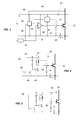
- a variable speed drive comprises a rectifier stage R responsible for rectifying an AC three-phase voltage from an external power supply network A, in order to provide a DC bus voltage Vb.
- the rectifier stage R comprises two electronic power components 14a, 14b per phase. These components 14a, 14b are for example diodes and / or thyristors.
- the example of figure 1 has a thyristor 14a coupled with a diode 14b for each phase of the network A.
- the drive shown in FIG. figure 1 comprises two bus capacitors 18 coupled to two balancing resistors 17 which make it possible to balance the voltage between these two capacitors.
- the drive controller then comprises an inverter stage O enabling, from the DC bus Vb, to control an electric motor M with a voltage of variable amplitude and frequency, by means of pulse width modulation control ( MLI or PWM).
- the inverter stage is provided with two electronic power switches 15a, 15b per phase.
- Each switch 15a, 15b is a JFET (junction-field effect) transistor of normally closed type (that is to say in the on state in the absence of a voltage on the gate of the transistor) which is realized by silicon carbide (SiC).
- any high band gap material could be used, say having a low resistance in the conducting state R dson and able to withstand high voltages (greater than 1000 V), such as for example gallium nitride (GaN).
- GaN gallium nitride
- a first solution described in figure 1 is to supply the switching power supply 11 directly from the external AC network A and to use, in the rectifier stage R, thyristors 14a whose control devices are powered by the switching power supply 11. Thus, as long as the voltage Vs is not present, the thyristors 14a are not controlled and the bus voltage Vb does not appear.
- Another solution is for example to supply the switching power supply 11 directly from the external AC network A, upstream of a line contactor (not shown) present at the input of the drive.
- the coil of this line contactor is controlled from the voltage Vs.
- the rectifier stage R of the drive is then not powered and the bus voltage Vb does not appear.
- the rectifier stage R may comprise only diodes 14a, 14b.
- the figure 2 shows an existing control device of a normally closed JFET transistor type electronic switch 15, made for example of SiC.
- a JFET transistor 15 is controlled by applying a negative voltage V GS between the gate G and the source S.
- V GS negative voltage
- the transistor 15 In the absence of voltage V GS between gate G and source S or in the presence of a positive voltage V GS , the transistor 15 is passing between the drain D and the source S, that is to say that the voltage V DS is zero.
- V GS negative voltage
- V GS negative for example of the order of -15 volts.
- the controller comprises a gate control circuit 30 (also called Gate Driver) which is a power amplifier circuit enabling the control of the gate G, from a control signal 37.
- this main gate control circuit 30 may be of the type "Push-Pull", “Reversed Push-Pull” or “Totem Pole” and realized with bipolar transistors or MOSFET transistors.
- the output 39 of the main gate control circuit 30 is connected to the gate G of the JFET transistor 15 via a resistor 31.
- the control signal 37 of the transistor 15 comes for example from the control unit 24 of the speed variator.
- the control device of the figure 2 also comprises one or more fault detection modules 33, 34, 35, the purpose of which is to allow the transistor 15 to be kept in the OFF state if one of these faults occurs.
- the outputs of these detection modules 33, 34, 35 form the inputs of an OR logic gate 32, the output of which provides a deactivation input (or "Disable”") D IS to the main gate control circuit 30.
- D IS input is in state 1, it means that the gate control circuit 30 must force the transistor 15 to the OFF state (whatever the state of the control signal C) and thus supply a negative voltage V GS (of the order of -15 V) on the gate G.
- a first undervoltage detection module 33 serves to detect the occurrence of a fall in the voltage Vs of the power supply 11 below a predetermined threshold. This voltage drop can in particular come from the power off of the drive, or from a fault or a short circuit of the power supply 11, the buffer capacitor 21 or the gate control circuit 30.
- a second short-circuit detection module 35 is used to detect the appearance of a short-circuit in the JFET transistor 15.
- the short-circuit detection module 35 compares the control signal 37 with the actual voltage across the terminals. JFET transistor 15 to detect a possible short circuit.
- a third overvoltage detection module 34 is used to detect the occurrence of an overvoltage at the terminals of the JFET transistor 15. This overvoltage can for example occur when an attempt is made to open the JFET transistor 15 while a short circuit exists. on the power line P of the JFET transistor 15.
- the control device is powered by a main source of energy delivering a main voltage Vs between positive and negative terminals 29.
- this main source of energy preferably comes from the power supply. 11, associated with a diode of rectification 22 and a main capacitor 21 serving as an energy buffer for the voltage Vs.
- the control device also comprises an auxiliary energy source 25 which is charged by means of the voltage Vs through a charge diode 26.
- this auxiliary energy source is a simple auxiliary reserve capacitor 25.
- the negative terminal of the auxiliary capacitor 25 is connected to the negative terminal 29 of the main capacitor 21.
- the positive terminal of the auxiliary capacitor 25 is connected to the source S of the JFET transistor 15 and to the positive terminal 28 of the main capacitor.
- the auxiliary back-up capacitor 25 may be a chemical capacitor, which has the advantage of being less expensive, or preferably a tantalum or polypropylene capacitor, which has the advantage of being more robust.
- This load diode 26 serves to prevent the auxiliary capacity 25 from being discharged in all the elements placed in parallel with the main capacitance 21, such as the elements 33, 35, 30, when the voltage Vs is lower than the voltage V R at the terminals of the auxiliary capacitor 25. It is placed downstream of the circuit closest to the JFET transistor 15 (in the occurrences the circuit 30 in the figures), that is to say between the auxiliary capacitor 25 and the connections of the circuit 30. Its cathode is directed towards the positive terminal of the auxiliary capacitor 25 and its anode is directed towards the positive terminal 28. It could also have had the charge diode 26 between the negative terminals of the capacitors 21, 25, its cathode being then connected to the negative terminal of the auxiliary capacitor 25 and its anode connected to the negative terminal 29.
- the auxiliary capacitor 25 When the voltage Vs appears, the auxiliary capacitor 25 is charged automatically, because the charging diode 26 is on as long as the voltage V R is lower than the voltage Vs. When the voltage Vs drops and falls below the voltage V R , the Auxiliary capacitance 25 provides a voltage reserve for supplying the gate control circuit 30, whose output 39 must provide a negative voltage V GS . The size of the auxiliary capacitance 25 must be calculated to obtain a negative voltage V GS which is able to keep the JFET transistor 15 in the off state OFF, for a time T sufficient to ensure that the bus capacitors of the variator are well discharged (for example of the order of 10 minutes). Indeed, as long as the bus capacitors are not discharged, it is not necessary for the JFET transistor 15 to return to the ON state, for safety reasons.
- any gate driver circuit 30 consumes energy and generates leak currents that can be significant (for example greater than 1 mA).
- the auxiliary capacity 25 will therefore be discharged rather quickly in the circuit 30. It is then necessary a very strong auxiliary capacity 25 to arrive to provide the sufficient energy reserve to block the JFET transistor 15 throughout the duration T. This therefore causes problems of feasibility, cost and dimensions, particularly for a three-phase inverter comprising six JFET transistors 15 distinct in its inverter stage.
- one of the aims of the invention is to design a control device for minimizing losses when the auxiliary capacitance 25 is to supply the voltage V GS to keep the JFET transistor 15 in the OFF state during the duration T.
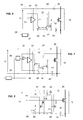
- the invention proposes to add a protective switching device to the control device. This switching member is switchable between two positions and is arranged so that, in one of these two positions, the negative terminal of the auxiliary capacitor 25 is connected to the gate G of the transistor 15 without passing through the gate control circuit. 30, so that in this position the auxiliary capacitance 25 supplies the gate 30 of the normally closed JFET transistor 15 to keep it OFF and the auxiliary capacitor 25 can not be discharged by other components.
- the protective switching member is an electromagnetic switch 41.
- the protective switching device is an electronic switch 51.
- the control device of a JFET switch is powered by a main source of energy delivering a main voltage Vs between the terminals 28 and 29.
- this main source of energy is preferably the switching power supply 11.
- the control device also comprises an auxiliary energy source 25 which is charged by the voltage Vs through a charge diode 26, in a manner identical to the device of the figure 2 described above.
- the control device comprises a main gate control circuit 30 (or Gate Driver) for controlling the gate G, from the control signal 37 which comes for example from the control unit 24 of the speed controller.
- a single fault detection module is presented (in this case a short-circuit detection module 35 of the JFET transistor), the output 36 of this detection module being directly connected to the input D IS of the control circuit grid 30.
- the output 39 of the main gate control circuit 30 is connected to the gate G of the JFET transistor 15 via a resistor 31. Unlike the figure 2 , an electromagnetic switch type protection switch is placed between the output 39 and the gate G.
- This electromagnetic switch comprises a movable contact 41 which is switchable between two positions under the action of an auxiliary control circuit 40.
- the electromagnetic switch makes it possible to connect the gate G of the JFET transistor 15 to the output 39 of the gate control circuit 30.
- the electromagnetic switch isolates the gate G of the output 39 and connects the gate G to the negative terminal of the auxiliary reserve capacitor 25, possibly via a resistor 27.
- the negative terminal of the auxiliary capacitor 25 is connected to the gate G without going through the gate control circuit 30.
- the resistor 27 is preferably large enough to limit the current variation dl / dt during the blocking of the JFET transistor 15 and thus to avoid any overvoltages.
- the electromagnetic switch is designed so that in the absence of power from its control coil, the movable contact 41 is always maintained in the second position, for example by means of magnetic return means (permanent magnet) or elastic.
- magnetic return means permanent magnet
- MEMS Micro Electro Magnetic Switch
- the auxiliary control circuit 40 comprises a control coil 43 which actuates the movable contact 41 of the electromagnetic switch.
- the first end of the coil 43 is connected to the positive terminal 28.
- the second end of the coil 43 is connected to the negative terminal 29 via a transistor 44.
- the transistor 44 is a bipolar transistor NPN whose collector is connected to the second end of the coil 43 and whose emitter is connected to the negative terminal 29.
- the base of this bipolar transistor 44 is connected to the positive terminal 28 at the through a resistor and a sensing member of a minimum voltage threshold Vs, such as a Zener diode 45.
- the auxiliary control circuit 40 could also be composed with field effect transistors. of MOSFET type instead of bipolar transistors.
- the Zener diode 45 In normal operation, when the voltage Vs is present, the Zener diode 45 conducts, so the transistor 44 is on and a current flows in the control coil 43. The movable contact 41 is then held in its first position, which allows to connect the gate G to the output 39 of the gate control circuit 30. The auxiliary capacity 25 is charged via the diode 26.
- the source S of the JFET transistor 15 is connected to the positive terminal of the auxiliary capacitor 25 and the gate G of the JFET transistor 15 is connected to the negative terminal of the auxiliary capacitor 25 via the resistor 27.
- auxiliary power supply comprising only the JFET transistor 15, the auxiliary capacitor 25 and the resistor 27.
- the diode 26 prevents the auxiliary capacitor 25 from discharging towards the capacitor 21 and any other circuit connected in parallel with this main source, as long as the voltage V R is greater than the voltage Vs.
- the auxiliary capacitor 25 can therefore no longer be discharged elsewhere than in the JFET transistor to provide a negative voltage V GS .
- a JFET transistor generates very little leakage current on its Grid-Source capacity.
- the auxiliary circuit 40 further comprises a second transistor 48 whose collector is connected (via a resistor) to the base of the transistor 44 and whose emitter is connected to the negative terminal 29.
- the base of the second transistor 48 is connected (via a resistor) to the output 36 of the short-circuit detection module 35 of the JFET.
- this module 35 detects a short circuit, its output 36 goes to state 1, which makes the transistor 48 turn and the transistor 44 goes to the blocking state.
- the coil 43 is no longer powered and the movable contact 41 returns to its second position.
- the gate G is isolated from the gate control 30 when a short circuit of the JFET transistor 15 is detected.
- Another option would also be to manage the output of an overvoltage detection module 34 in the auxiliary circuit 40.
- this second movable contact avoids any leakage currents of the diode 26 when it is blocked, thereby lengthening the duration T during which the auxiliary capacitance 25 can maintain the JFET transistor 15 OFF state. It is also prevented from discharging the main capacitance 21 into the auxiliary capacitance 25 due to a possible short circuit of the Source Grid connections of the JFET transistor 15 when it dies in short circuit. This avoids propagating the fault of the JFET transistor in the gate control circuit 30.
- the Figures 6 to 8 show several examples of a second embodiment of the invention in which the protective switching element is not an electromagnetic switch but comprises a first electronic switch 51.
- This electronic switch 51 is preferably an N-channel MOSFET transistor. which has the advantage of generating very little leak when in the ON state.
- control device of the JFET switch 15 is powered by a main energy source and an auxiliary energy source 25, in a manner identical to the device of the figure 3 described above.
- the control device comprises a main gate control circuit 30 (or Gate Driver) for controlling the gate G, from the control signal 37 which comes for example from the control unit 24 of the speed variator.
- the output 39 of the main gate control circuit 30 is connected to the gate G of the JFET transistor 15 via a resistor.
- the source of the MOSFET transistor 51 is connected to the negative terminal of the auxiliary capacitor 25.
- the drain of the MOSFET transistor 51 is connected to the gate G of the JFET transistor 15 via a resistor 57.
- the gate of the MOSFET transistor 51 is controlled by a signal control circuit from the auxiliary control circuit 50.
- This auxiliary control circuit 50 can be realized with transistors in bipolar technology, as shown below, or equivalent in MOSFET technology.
- the figure 6 details a first example of the auxiliary control circuit 50 fulfilling the voltage undervoltage detection function Vs.
- the auxiliary control circuit 50 comprises a bipolar transistor 54 whose collector is connected to the positive terminal of the auxiliary capacitor 25 via a resistance and at the gate of the MOSFET transistor 51, whose Transmitter is connected to the negative terminal of the auxiliary capacitor 25 and whose Base is connected to the positive terminal 28 through a resistor and a Zener diode 55
- the operation of the auxiliary control circuit 50 is as follows:
- the Zener diode 55 conducts and the transistor 54 is conducting. In this case the collector of the transistor 54 is 0 and the electronic switch 51 does not receive a control signal. The electronic switch 51 is therefore in a first state non-conducting or blocked. In this case, the gate G of the JFET transistor 15 is controlled solely by the output 39 of the gate control circuit 30, because the gate G is not connected to the negative terminal of the capacitor 25.
- the collector of the transistor 54 is reset to 1 because it is connected (via a resistor) to the positive terminal of the auxiliary capacitor 25.
- the electronic switch 51 then receives a control signal which switches it to a second state. passing.
- the gate G of the JFET transistor 15 is then directly connected to the negative terminal of the auxiliary capacitor 25, via the resistor 57.
- an auxiliary supply circuit comprising the JFET transistor 15, the auxiliary capacitor 25, the electronic switch 51 and the resistor 57.
- JFET transistor 15 at a negative potential determined by the voltage V R across the auxiliary capacitor 25, by short-circuiting the output 39 of the gate control circuit 30.
- the electronic switch 51 is a transistor MOSFET generating very little on-state leakage current, this solution also makes it possible to minimize the losses of the auxiliary circuit, and thus to obtain a very important duration T and / or a smaller auxiliary capacity size. In the absence of power supply, the electronic switch 51 remains in the second on state.
- the auxiliary control circuit 50 also comprises another bipolar transistor 53 whose collector is connected to the input D IS of the gate control circuit 30, whose Transmitter is connected to the negative terminal of the auxiliary capacitor 25 and whose base is connected to the base of the transistor 54 via a resistor.
- the Zener diode 55 In normal operation, when the voltage Vs is present, the Zener diode 55 conducts, so the transistor 53 is on and the input D IS of the gate control circuit 30 is equal to 0. As soon as the Zener diode 55 no longer conducts , the bipolar transistor 53 becomes a blocker, which forces the input D IS of the gate control circuit 30 to state 1 so as to suppress the voltage on the output 39.
- the figure 7 gives a second example of the auxiliary control circuit 50.
- the short-circuit detection function of the JFET transistor 15 is also processed.
- the control device comprises a short-circuit detection module 35 already previously described.
- the auxiliary control circuit 50 further comprises a bipolar transistor 58 whose collector is connected to the base of the transistor 54, whose emitter is connected to the negative terminal of the auxiliary capacitor 25 and whose base is connected to the output 36 of the module 35.
- This output 36 is also sent to an OR logic gate to be combined with the collector of the transistor 53.
- the module 35 detects a short circuit
- its output 36 goes to the state 1, which makes the transistor 58 passing and the transistor 54 becomes blocking.
- the electronic switch 51 switches into the second on state, and the gate G of the JFET transistor 15 is directly connected to the negative terminal of the auxiliary capacitor 25, via the resistor 57.
- a negative voltage is forced between the gate G and the source S of the JFET transistor 15 when a short circuit of the JFET transistor 15 is detected.
Abstract
Description
La présente invention se rapporte à un dispositif de commande d'un interrupteur électronique de puissance de type transistor JFET (Junction Field Effect Transistor ou Transistor à Effet de Champ à Jonction) réalisé par exemple en carbure de silicium (SiC ou Silicon Carbide). L'invention se propose d'utiliser de tels transistors JFET du type normalement fermé (ou "normally ON") pour la commutation d'importants courants de puissance et en particulier comme interrupteurs de puissance dans un étage onduleur d'un variateur de vitesse.The present invention relates to a control device of a JFET (Junction Field Effect Transistor) transistor type electronic power switch made for example of silicon carbide (SiC or Silicon Carbide). The invention proposes to use such JFET transistors of the normally closed type (or "normally ON") for switching large power currents and in particular as power switches in an inverter stage of a variable speed drive.
Un transistor JFET est un interrupteur électronique connu qui comporte une Grille de commande dont la fonction est d'autoriser ou non le passage d'un courant entre un Drain et une Source. Un tel transistor est dit du type normalement fermé (ou Normally ON) si la tension VDS entre le Drain et la Source est nulle lorsque la tension VGS entre la Grille et la Source est nulle. Cela signifie que le chemin Drain - Source est passant ou conducteur en l'absence de tension de commande VGS entre Grille et Source. Inversement un transistor JFET est dit du type normalement ouvert (ou normally OFF) si le chemin Drain - Source n'est pas conducteur en l'absence de tension VGS entre Grille et Source.A JFET transistor is a known electronic switch which includes a control gate whose function is to allow or not the passage of a current between a drain and a source. Such a transistor is said to be of the normally closed type (or Normally ON) if the voltage V DS between the drain and the source is zero when the voltage V GS between the gate and the source is zero. This means that the Drain - Source path is conducting or conducting in the absence of V GS control voltage between Grid and Source. Conversely, a JFET transistor is said to be of the normally open (or normally OFF) type if the Drain - Source path is not conductive in the absence of V GS voltage between Grid and Source.
Il s'avère qu'un interrupteur électronique JFET de type normalement fermé offre de bien meilleures performances que d'autres types d'interrupteurs électroniques de puissance commandés en tension, tels que des MOSFET, des IGBT ou même des JFET de type normalement ouvert. En effet, un tel interrupteur présente notamment les avantages d'être plus rapide à commuter, de générer moins de pertes à l'état passant, d'avoir une meilleure tenue en température, d'avoir une taille plus petite et de coûter moins cher.It turns out that a normally closed type JFET electronic switch offers much better performance than other types of voltage controlled electronic power switches, such as MOSFETs, IGBTs or even normally open type JFETs. Indeed, such a switch has the advantages of being faster to switch, to generate less losses in the on state, to have a better temperature resistance, to have a smaller size and to cost less .
Néanmoins, tout interrupteur électronique du type normalement fermé présente l'inconvénient d'être à l'état passant (ou fermé) en l'absence de tension de commande sur sa Grille (Gate). Cette caractéristique n'est pas sécurisante pour la commande de courants importants puisque cet interrupteur laisse passer le courant entre Drain et Source en l'absence de commande sur la Grille. Il en résulte évidemment des risques potentiels importants pour la sécurité des biens et des personnes.Nevertheless, any electronic switch of the normally closed type has the disadvantage of being in the on state (or closed) in the absence of control voltage on its gate. This characteristic is not reassuring for the control of large currents since this switch allows current to pass between Drain and Source in the absence of control on the grid. This obviously results in significant potential risks to the safety of property and people.
De façon usuelle, un variateur de vitesse de type convertisseur de fréquence comporte un étage redresseur chargé de redresser une tension provenant d'une source extérieure d'alimentation électrique alternative (par exemple un réseau électrique triphasé 380Vac) pour fournir une tension continue sur un bus continu (par exemple de l'ordre de 400 à 800Vcc ou plus suivant les conditions d'utilisation). Un ou plusieurs condensateurs de bus de forte capacité sont habituellement utilisés pour maintenir constante la tension du bus continu.Usually, a frequency converter of the type of frequency converter comprises a rectifier stage responsible for straightening a voltage coming from a source external AC power supply (for example a three-phase 380Vac electrical network) for supplying a DC voltage on a DC bus (for example of the order of 400 to 800Vcc or more depending on the conditions of use). One or more high capacity bus capacitors are usually used to keep the DC bus voltage constant.
Le variateur de vitesse comporte ensuite un étage onduleur chargé de commander un moteur électrique avec une tension d'amplitude et de fréquence variables, à partir de ce bus continu. Pour cela, l'étage onduleur est doté de deux interrupteurs électroniques de puissance par phase. Chaque interrupteur est commandé par un circuit de commande alimenté par une alimentation à découpage (alimentation de type SMPS : Switched Mode Power Supply) du variateur de vitesse.The speed controller then comprises an inverter stage responsible for controlling an electric motor with a voltage of variable amplitude and frequency, from this DC bus. For this, the inverter stage is equipped with two electronic power switches per phase. Each switch is controlled by a control circuit powered by a switching power supply (SMPS supply: Switched Mode Power Supply) of the drive controller.
Ainsi, si l'on veut utiliser des interrupteurs électroniques du type normalement fermé dans l'étage onduleur d'un variateur de vitesse, plusieurs risques peuvent alors apparaître :
- A la mise sous tension du variateur, il faut s'assurer que les circuits de commande des interrupteurs électroniques sont correctement alimentés, pour pouvoir ouvrir ces interrupteurs avant l'apparition de la tension sur le bus continu du variateur,
- A la mise hors tension, il faut s'assurer du maintien de l'ouverture des interrupteurs électroniques, tant que le ou les condensateurs de bus ne sont pas déchargés, par exemple dans des résistances d'équilibrage, sachant que la décharge de ces condensateurs peut parfois durer jusqu'à plusieurs minutes,
- Lors de l'apparition d'un défaut, il faut également s'assurer du maintien de l'ouverture des interrupteurs tant que le ou les condensateurs du bus continu ne sont pas déchargés. Un tel défaut peut provenir notamment d'un court-circuit dans le circuit de commande, d'une perte de l'alimentation du circuit de commande, etc...
- When the drive is powered up, it must be ensured that the control circuits of the electronic switches are correctly powered, in order to be able to open these switches before the occurrence of the voltage on the DC bus of the drive,
- When switching off, make sure that the electronic switches are open, as long as the bus capacitor (s) are not discharged, for example in balancing resistors, knowing that the discharge of these capacitors can sometimes last up to several minutes,
- When a fault occurs, it must also be ensured that the switches remain open as long as the capacitor (s) of the DC bus are not discharged. Such a fault can come in particular from a short circuit in the control circuit, a loss of the power supply of the control circuit, etc.
Pour éviter ces risques, il existe déjà une solution dans laquelle chaque transistor JFET de type normalement fermé est monté en série avec un autre composant auxiliaire de type normalement ouvert, tel que par exemple un transistor CASCODE. Cette solution nécessite cependant l'utilisation de deux transistors en série pour chaque interrupteur de puissance, ce qui entraîne notamment une augmentation des coûts et une augmentation des pertes par conduction.To avoid these risks, there is already a solution in which each normally closed type JFET transistor is connected in series with another normally open type auxiliary component, such as for example a CASCODE transistor. This solution, however, requires the use of two transistors in series for each power switch, which leads in particular to an increase in costs and an increase in losses by conduction.
Le but de l'invention est donc de proposer l'utilisation de transistors JFET de type normalement fermé comme interrupteurs de puissance dans un étage onduleur d'un variateur de vitesse, grâce à un dispositif de commande capable d'éviter les inconvénients évoqués ci-dessus, à savoir proposer une solution simple qui permette d'éviter les risques lors des mises sous/hors tension et lors de défauts.The object of the invention is therefore to propose the use of JFET transistors of normally closed type as power switches in an inverter stage of a variable speed drive, thanks to a control device capable of avoiding the drawbacks mentioned above. above, namely to propose a simple solution that avoids the risks when power on / off and during defects.
Pour cela, l'invention décrit un dispositif de commande d'un interrupteur électronique de puissance de type JFET de type normalement fermé, le dispositif de commande comprenant un circuit principal de commande de grille alimenté par une source principale d'énergie pour piloter la grille de l'interrupteur JFET. Le dispositif de commande comporte un organe de commutation de protection commutable entre deux positions, un circuit auxiliaire de commande pilotant l'organe de commutation de protection, et une source auxiliaire d'énergie alimentée par ladite source principale d'énergie. La borne négative de la source auxiliaire d'énergie est connectée à la grille de l'interrupteur JFET sans passer par ledit circuit principal de commande de grille dans l'une des deux positions de l'organe de commutation de protection, et la borne positive de la source auxiliaire d'énergie est connectée à la source de l'interrupteur JFET.For this purpose, the invention describes a device for controlling a normally closed type JFET type electronic power switch, the control device comprising a main gate control circuit powered by a main power source for driving the gate. of the JFET switch. The control device comprises a switchable protection switching element between two positions, an auxiliary control circuit driving the protection switching element, and an auxiliary power source powered by said main energy source. The negative terminal of the auxiliary power source is connected to the gate of the JFET switch without passing through said main gate control circuit in one of the two positions of the protection switching member, and the positive terminal the auxiliary power source is connected to the source of the JFET switch.
Selon une caractéristique, l'organe de commutation de protection comporte un commutateur électromagnétique doté d'un contact mobile entre deux positions sous l'action d'une bobine de commande du circuit auxiliaire de commande, ledit contact mobile étant commutable entre une première position dans laquelle la grille de l'interrupteur JFET est reliée au circuit principal de commande de grille et une seconde position dans laquelle la grille de l'interrupteur JFET est reliée à la borne négative de la source auxiliaire d'énergie. En l'absence d'alimentation de la bobine de commande, le contact mobile est maintenu dans la seconde position.According to one characteristic, the protective switching device comprises an electromagnetic switch having a movable contact between two positions under the action of a control coil of the auxiliary control circuit, said movable contact being switchable between a first position in wherein the gate of the JFET switch is connected to the main gate control circuit and a second position in which the gate of the JFET switch is connected to the negative terminal of the auxiliary power source. In the absence of power to the control coil, the movable contact is maintained in the second position.
Selon une autre caractéristique, l'organe de commutation de protection comprend un premier commutateur électronique qui est placé entre la grille de l'interrupteur JFET et la borne négative de la source auxiliaire d'énergie, et qui est piloté par le circuit auxiliaire de commande entre un premier état non-passant dans lequel la grille de l'interrupteur JFET n'est pas reliée à la borne négative de la source auxiliaire d'énergie et un second état passant dans lequel la grille de l'interrupteur JFET est reliée à la borne négative de la source auxiliaire d'énergie.According to another characteristic, the protection switching device comprises a first electronic switch which is placed between the gate of the JFET switch and the negative terminal of the auxiliary energy source, and which is controlled by the auxiliary control circuit. between a first non-conducting state in which the gate of the JFET switch is not connected to the negative terminal of the auxiliary energy source and a second passing state in which the gate of the JFET switch is connected to the negative terminal of the auxiliary power source.
D'autres caractéristiques et avantages vont apparaître dans la description détaillée qui suit en se référant à un mode de réalisation donné à titre d'exemple et représenté par les dessins annexés sur lesquels :
- la
figure 1 montre une architecture simplifiée classique d'un variateur de vitesse utilisant plusieurs interrupteurs de puissance JFET, - la
figure 2 décrit un dispositif de commande connu d'un interrupteur de puissance JFET de type normalement fermé ou normally ON, - la
figure 3 représente un premier mode de réalisation d'un dispositif de commande d'un interrupteur de puissance JFET selon l'invention, - la
figure 4 détaille un exemple d'un circuit auxiliaire de commande du commutateur électromagnétique selon le premier mode de réalisation, - la
figure 5 donne une variante du premier mode de réalisation, - la
figure 6 montre un second mode de réalisation d'un dispositif de commande d'un interrupteur de puissance JFET selon l'invention, - les
figures 7 & 8 donnent des variantes du second mode de réalisation.
- the
figure 1 shows a simplified simplified architecture of a variable speed drive using several JFET power switches, - the
figure 2 discloses a known control device of a normally closed or normally ON type JFET power switch, - the
figure 3 represents a first embodiment of a device for controlling a JFET power switch according to the invention, - the
figure 4 details an example of an auxiliary control circuit of the electromagnetic switch according to the first embodiment, - the
figure 5 gives a variant of the first embodiment, - the
figure 6 shows a second embodiment of a device for controlling a JFET power switch according to the invention, - the
Figures 7 & 8 give variants of the second embodiment.
En référence à la
Le variateur de vitesse comporte ensuite un étage onduleur O permettant, à partir du bus continu Vb, de commander un moteur électrique M avec une tension d'amplitude et de fréquence variables, au moyen d'une commande par Modulation à Largeur d'Impulsions (MLI ou PWM). Pour cela, l'étage onduleur est doté de deux interrupteurs électroniques de puissance 15a,15b par phase. Chaque interrupteur 15a,15b est un transistor JFET (à Effet de Champ à Jonction) de type normalement fermé (c'est-à-dire à l'état passant en l'absence de tension sur la Grille du transistor) qui est réalisé en carbure de silicium (SiC). D'autres matériaux que le carbure de silicium pourraient aussi être utilisés : ainsi, on pourrait utiliser tout matériau à grande énergie de bande interdite (appelé également matériau à grand gap ou "wide-band gap material"), c'est-à-dire présentant une faible résistance à l'état passant Rdson et capable de supporter des tensions importantes (supérieures à 1000 V), comme par exemple du nitrure de gallium (GaN).The drive controller then comprises an inverter stage O enabling, from the DC bus Vb, to control an electric motor M with a voltage of variable amplitude and frequency, by means of pulse width modulation control ( MLI or PWM). For this, the inverter stage is provided with two
Ces dispositifs de commande sont alimentés par une alimentation à découpage 11 (SMPS : Switched Mode Power Supply) du variateur de vitesse, qui fournit une tension continue Vs à partir du réseau d'alimentation A. La tension Vs est notamment utilisée pour alimenter l'unité de commande du variateur (non représentée sur la
A cause de l'utilisation d'interrupteurs de puissance 15a,15b de type normalement fermé, il faut évidemment s'assurer que les dispositifs de commande de ces interrupteurs 15a,15b sont alimentés correctement avant l'apparition de la tension de bus Vb, pour éviter un court-circuit dans l'étage onduleur O du variateur et/ou des courants intempestifs dans le moteur M. Il faut donc s'assurer que l'alimentation à découpage 11 fournit la tension Vs avant l'apparition de la tension de bus Vb.Due to the use of normally closed
Une première solution décrite en
Une autre solution consiste par exemple à alimenter l'alimentation à découpage 11 directement à partir du réseau alternatif extérieur A, en amont d'un contacteur de ligne (non représenté) présent à l'entrée du variateur. La bobine de ce contacteur de ligne est commandée à partir de la tension Vs. Ainsi, tant que la tension Vs n'est pas présente, le contacteur de ligne est ouvert. L'étage redresseur R du variateur n'est alors pas alimenté et la tension de bus Vb n'apparaît pas. Dans cette solution, l'étage redresseur R peut ne comporter que des diodes 14a,14b.Another solution is for example to supply the switching
La
Le dispositif de commande comporte un circuit principal de commande de grille 30 (appelé également Gate Driver) qui est un circuit amplificateur de puissance permettant la commande de la grille G, à partir d'un signal de commande 37. De façon connue, ce circuit principal de commande de grille 30 peut être du type "Push-Pull", "Reversed Push-Pull" ou "Totem Pôle" et réalisé avec des transistors bipolaires ou des transistors MOSFET. La sortie 39 du circuit principal de commande de grille 30 est reliée à la grille G du transistor JFET 15 par l'intermédiaire d'une résistance 31. Le signal de commande 37 du transistor 15 provient par exemple de l'unité de commande 24 du variateur de vitesse.The controller comprises a gate control circuit 30 (also called Gate Driver) which is a power amplifier circuit enabling the control of the gate G, from a
Suivant les fonctionnalités souhaitées, le dispositif de commande de la
Un premier module de détection de sous-tension 33 sert à détecter l'apparition d'une chute de la tension Vs de l'alimentation 11 en dessous d'un seuil prédéterminé. Cette chute de tension peut notamment provenir soit de la mise hors tension du variateur, soit d'un défaut ou d'un court-circuit de l'alimentation 11, de la capacité tampon 21 ou du circuit de commande de grille 30.A first
Un deuxième module de détection de court-circuit 35 sert à détecter l'apparition d'un court-circuit dans le transistor JFET 15. Le module de détection de court-circuit 35 compare le signal de commande 37 avec la tension réelle aux bornes du transistor JFET 15 pour détecter un éventuel court-circuit.A second short-
Un troisième module de détection de surtension 34 sert à détecter l'apparition d'une surtension aux bornes du transistor JFET 15. Cette surtension peut par exemple survenir lorsque l'on cherche à ouvrir le transistor JFET 15 alors qu'un court-circuit existe sur la ligne de puissance P du transistor JFET 15.A third
Le dispositif de commande est alimenté par une source principale d'énergie délivrant une tension principale Vs entre les bornes positive 28 et négative 29. Dans le cadre d'un variateur de vitesse, cette source principale d'énergie provient préférentiellement de l'alimentation à découpage 11, associée à une diode de redressement 22 et une capacité principale 21 servant de tampon d'énergie pour la tension Vs.The control device is powered by a main source of energy delivering a main voltage Vs between positive and
Le dispositif de commande comporte aussi une source auxiliaire d'énergie 25 qui est chargée à l'aide de la tension Vs au travers d'une diode de charge 26. Préférentiellement, cette source auxiliaire d'énergie est une simple capacité auxiliaire de réserve 25. La borne négative de la capacité auxiliaire 25 est reliée à la borne négative 29 de la capacité principale 21. La borne positive de la capacité auxiliaire 25 est reliée à la source S du transistor JFET 15 et à la borne positive 28 de la capacité principale 21 via la diode de charge 26. La capacité auxiliaire de réserve 25 peut être une capacité chimique, qui présente l'avantage d'être moins coûteuse, ou préférentiellement une capacité tantale ou polypropylène, qui présente l'avantage d'être plus robuste.The control device also comprises an
Cette diode de charge 26 sert à éviter que la capacité auxiliaire 25 ne se décharge dans tous les éléments placés en parallèle avec la capacité principale 21, tels que les éléments 33, 35, 30, lorsque la tension Vs est inférieure à la tension VR aux bornes de la capacité auxiliaire 25. Elle est placée en aval du circuit le plus proche du transistor JFET 15 (en l'occurrences le circuit 30 sur les figures), c'est-à-dire entre la capacité auxiliaire 25 et les raccordements du circuit 30. Sa cathode est dirigée vers la borne positive de la capacité auxiliaire 25 et son anode est dirigée vers la borne positive 28. On aurait pu aussi disposer la diode de charge 26 entre les bornes négatives des capacités 21,25, sa cathode étant alors reliée à la borne négative de la capacité auxiliaire 25 et son anode reliée à la borne négative 29.This
Lorsque la tension Vs apparaît, la capacité auxiliaire 25 se charge automatiquement, car la diode de charge 26 est passante tant que la tension VR est inférieure à la tension Vs. Lorsque la tension Vs chute et devient inférieure à la tension VR, la capacité auxiliaire 25 fournit une réserve de tension pour alimenter le circuit de commande de grille 30, dont la sortie 39 doit fournir une tension VGS négative. La taille de la capacité auxiliaire 25 doit être calculée pour obtenir une tension négative VGS qui soit capable de maintenir le transistor JFET 15 à l'état bloqué OFF, durant une durée T suffisante pour s'assurer que les condensateurs de bus du variateur sont bien déchargés (par exemple de l'ordre de 10 minutes). En effet, tant que les condensateurs de bus ne sont pas déchargés, il ne faut pas que le transistor JFET 15 repasse à l'état passant ON, pour des raisons de sécurité.When the voltage Vs appears, the
Or, il se trouve que tout circuit de commande de grille 30 (Gate driver) consomme de l'énergie et génère des courants de fuite qui peuvent être importants (par exemple supérieurs à 1 mA). La capacité auxiliaire 25 va donc se décharger assez rapidement dans le circuit 30. Il faut alors une très forte capacité auxiliaire 25 pour arriver à fournir la réserve d'énergie suffisante permettant de bloquer le transistor JFET 15 pendant toute la durée T. Cela entraîne donc des problèmes de faisabilité, de coût et de dimensions, en particulier pour un variateur triphasé comprenant six transistors JFET 15 distincts dans son étage onduleur.However, it happens that any
C'est pourquoi, l'un des buts de l'invention est de concevoir un dispositif de commande permettant de minimiser les pertes lorsque la capacité auxiliaire 25 doit fournir la tension VGS pour maintenir le transistor JFET 15 à l'état bloqué OFF pendant la durée T. Pour cela, l'invention propose de rajouter un organe de commutation de protection au dispositif de commande. Cet organe de commutation est commutable entre deux positions et est agencé pour que, dans l'une de ces deux positions, la borne négative de la capacité auxiliaire 25 soit reliée à la grille G du transistor 15 sans passer par le circuit de commande de grille 30, de sorte que dans cette position la capacité auxiliaire 25 alimente la grille 30 du transistor JFET 15 normalement fermé pour le maintenir à l'état OFF et la capacité auxiliaire 25 ne peut pas être déchargée par d'autres composants.Therefore, one of the aims of the invention is to design a control device for minimizing losses when the
Selon un premier mode de réalisation de l'invention représenté dans les
En référence à la
Comme pour la
La sortie 39 du circuit principal de commande de grille 30 est reliée à la grille G du transistor JFET 15 par l'intermédiaire d'une résistance 31. Contrairement à la
Ce commutateur électromagnétique comporte un contact mobile 41 qui est commutable entre deux positions sous l'action d'un circuit auxiliaire de commande 40.This electromagnetic switch comprises a
Dans la première position du contact mobile 41, le commutateur électromagnétique permet de raccorder la grille G du transistor JFET 15 à la sortie 39 du circuit de commande de grille 30. Dans la seconde position du contact mobile 41, le commutateur électromagnétique isole la grille G de la sortie 39 et raccorde la grille G à la borne négative de la capacité auxiliaire de réserve 25, via éventuellement une résistance 27. Ainsi dans cette seconde position, la borne négative de la capacité auxiliaire 25 est connectée à la grille G sans passer par le circuit de commande de grille 30. La résistance 27 est de préférence assez importante de façon à limiter la variation de courant dl/dt lors du blocage du transistor JFET 15 et donc éviter d'éventuelles surtensions.In the first position of the
Le commutateur électromagnétique est conçu pour qu'en l'absence d'alimentation de sa bobine de commande, le contact mobile 41 soit toujours maintenu dans la seconde position, par exemple grâce à des moyens de rappel magnétiques (aimant permanent) ou élastiques. Préférentiellement, on utilise un commutateur électromagnétique de type MEMS (Micro Electro-Magnétic Switch) dont la consommation d'énergie, l'encombrement et le temps de réponse sont très faibles et qui ne génère pas de rebond.The electromagnetic switch is designed so that in the absence of power from its control coil, the
Un exemple d'un circuit auxiliaire de commande 40 est détaillé aux
En fonctionnement normal, lorsque la tension Vs est présente, la diode Zener 45 conduit, donc le transistor 44 est passant et un courant circule dans la bobine de commande 43. Le contact mobile 41 est alors maintenu dans sa première position, ce qui permet de relier la grille G à la sortie 39 du circuit de commande de grille 30. La capacité auxiliaire 25 se charge via la diode 26.In normal operation, when the voltage Vs is present, the
Quand la tension Vs chute et passe sous le seuil minimum de déclenchement déterminé par la diode Zener 45, celle-ci ne conduit plus et le transistor 44 devient bloquant. Aucun courant ne circulant alors dans la bobine de commande 43, le contact mobile 41 est automatiquement et rapidement rappelé dans sa seconde position (grâce aux moyens de rappel) dans laquelle la grille G est reliée à la borne négative de la capacité auxiliaire 25.When the voltage Vs drops below the minimum tripping threshold determined by the
Ainsi, lorsque le contact mobile 41 du commutateur électromagnétique est dans la seconde position (comme indiqué aux
La capacité auxiliaire 25 ne peut donc plus se décharger ailleurs que dans le transistor JFET pour fournir une tension VGS négative. Or, on sait qu'un transistor JFET génère très peu de courant de fuite sur sa capacité Grille-Source.The
Cette solution simple permet ainsi de minimiser énormément toutes les pertes du circuit auxiliaire, et donc d'obtenir une durée T beaucoup plus importante et/ou une taille de la capacité auxiliaire 25 plus faible. Dès que la tension Vs chute sous un seuil prédéterminé par la diode Zener 45, la grille G est isolée du circuit 30 et le circuit auxiliaire d'alimentation du transistor JFET 15 est créé. Le circuit auxiliaire de commande 40 fait ainsi office de module de détection de sous-tension de la tension Vs.This simple solution thus makes it possible to minimize all the losses of the auxiliary circuit enormously, and thus to obtain a much longer duration T and / or a smaller auxiliary capacity size. As soon as the voltage Vs falls below a predetermined threshold by the
Optionnellement, il est possible de rajouter aussi une fonction de protection du circuit de commande de grille 30 lorsque le transistor JFET 15 est en court-circuit. Pour cela, le circuit auxiliaire 40 comporte en plus un second transistor 48 dont le Collecteur est relié (via une résistance) à la Base du transistor 44 et dont l'Emetteur est relié à la borne négative 29. La Base du second transistor 48 est reliée (via une résistance) à la sortie 36 du module de détection de court-circuit 35 du JFET. Ainsi, lorsque ce module 35 détecte un court-circuit, sa sortie 36 passe à l'état 1, ce qui rend le transistor 48 passant et le transistor 44 passe à l'état bloquant. Dans ce cas, la bobine 43 n'est plus alimentée et le contact mobile 41 revient sur sa seconde position. Ainsi, on isole la grille G du circuit de commande de grille 30 quand un court-circuit du transistor JFET 15 est détecté. Une autre option consisterait aussi à gérer la sortie d'un module de détection de surtension 34 dans le circuit auxiliaire 40.Optionally, it is possible to add also a protection function of the
La
- En fonctionnement normal (c'est-à-dire quand un courant circule dans la bobine 43), le contact mobile 42 est dans sa première position et la borne positive 28 est reliée à la
diode 26, comme dans lafigure 4 . - Par contre, lorsque aucun courant ne circule dans la bobine 43, le contact mobile 42 est rappelé automatiquement sur sa seconde position, ce qui permet d'isoler la borne positive 28 de la
diode 26, et ainsi de déconnecter la source auxiliaire d'énergie 25 avec la source principale d'énergie.
- In normal operation (i.e., when a current flows in the coil 43), the
movable contact 42 is in its first position and thepositive terminal 28 is connected to thediode 26, as in FIG.figure 4 . - By cons, when no current flows in the
coil 43, themovable contact 42 is automatically recalled to its second position, which isolates thepositive terminal 28 of thediode 26, and thus disconnect theauxiliary power source 25 with the main source of energy.
Grâce à ce second contact mobile, on s'affranchit ainsi des éventuels courants de fuite de la diode 26 lorsqu'elle est bloquée, ce qui rallonge d'autant la durée T pendant laquelle la capacité auxiliaire 25 peut maintenir le transistor JFET 15 à l'état OFF. On empêche également de décharger la capacité principale 21 dans la capacité auxiliaire 25 suite à un éventuel court-circuit des connexions Grille Source du transistor JFET 15 lorsque celui-ci meurt en court-circuit. On évite ainsi de propager le défaut du transistor JFET dans le circuit de commande de grille 30.Thanks to this second movable contact, it avoids any leakage currents of the
Les
Dans la
Comme pour la
La Source du transistor MOSFET 51 est reliée à la borne négative de la capacité auxiliaire 25. Le Drain du transistor MOSFET 51 est relié à la grille G du transistor JFET 15 via une résistance 57. La Grille du transistor MOSFET 51 est commandée par un signal de commande provenant du circuit auxiliaire de commande 50. Ce circuit auxiliaire de commande 50 peut être réalisé avec des transistors en technologie bipolaire, comme présenté ci-dessous, ou de manière équivalente en technologie MOSFET.The source of the
La
En fonctionnement normal, lorsque la tension Vs est présente, la diode Zener 55 conduit et le transistor 54 est passant. Dans ce cas le Collecteur du transistor 54 est à 0 et le commutateur électronique 51 ne reçoit pas de signal de commande. Le commutateur électronique 51 est donc dans un premier état non-passant ou bloqué. Dans ce cas, la grille G du transistor JFET 15 est commandée uniquement par la sortie 39 du circuit de commande de grille 30, car la grille G n'est pas reliée à la borne négative de la capacité 25.In normal operation, when the voltage Vs is present, the
Dès que la tension Vs chute et passe sous le seuil minimum de déclenchement déterminé par la diode Zener 55, celle-ci ne conduit plus et le transistor 54 devient bloquant. Dans ce cas, le Collecteur du transistor 54 est rappelé à 1 car il est relié (via une résistance) à la borne positive de la capacité auxiliaire 25. Le commutateur électronique 51 reçoit alors un signal de commande qui le fait basculer dans un second état passant. La grille G du transistor JFET 15 est alors directement reliée à la borne négative de la capacité auxiliaire 25, via la résistance 57.As soon as the voltage Vs falls below the minimum trigger threshold determined by the
Ainsi, lorsque le commutateur électronique 51 est dans le second état passant, on crée avantageusement un circuit auxiliaire d'alimentation comprenant le transistor JFET 15, la capacité auxiliaire 25, le commutateur électronique 51 et la résistance 57. On force alors la grille G du transistor JFET 15 à un potentiel négatif déterminé par la tension VR aux bornes de la capacité auxiliaire 25, en court-circuitant la sortie 39 du circuit de commande de grille 30. Comme le commutateur électronique 51 est un transistor MOSFET générant très peu de courant de fuite à l'état passant, cette solution permet également de minimiser les pertes du circuit auxiliaire, et donc d'obtenir une durée T très importante et/ou une taille de la capacité auxiliaire 25 plus faible. En l'absence d'alimentation, le commutateur électronique 51 reste dans le second état passant.Thus, when the
Cependant, si le circuit de commande de grille 30 est en position haute (sortie 39 égale à Vs) lorsque le commutateur électronique 51 est à l'état passant, il faut forcer la sortie 39 à 0, pour éviter de faire passer un courant entre la sortie 39, la résistance 57 et la capacité auxiliaire 25. C'est pourquoi, le circuit auxiliaire de commande 50 comprend également un autre transistor bipolaire 53 dont le Collecteur est relié à l'entrée DIS du circuit de commande de grille 30, dont l'Emetteur est relié à la borne négative de la capacité auxiliaire 25 et dont la Base est reliée à la base du transistor 54 via une résistance.However, if the
En fonctionnement normal, lorsque la tension Vs est présente, la diode Zener 55 conduit, donc le transistor 53 est passant et l'entrée DIS du circuit de commande de grille 30 est égale à 0. Dès que la diode Zener 55 ne conduit plus, le transistor bipolaire 53 devient bloquant, ce qui force l'entrée DIS du circuit de commande de grille 30 à l'état 1 de façon à supprimer la tension sur la sortie 39.In normal operation, when the voltage Vs is present, the
La
Le circuit auxiliaire de commande 50 comporte en plus un transistor bipolaire 58 dont le Collecteur est relié à la Base du transistor 54, dont l'Emetteur est relié à la borne négative de la capacité auxiliaire 25 et dont la Base est reliée à la sortie 36 du module 35. Cette sortie 36 est envoyée également sur une porte logique OU pour être combinée avec le Collecteur du transistor 53. Ainsi, lorsque le module 35 détecte un court-circuit, sa sortie 36 passe à l'état 1, ce qui rend le transistor 58 passant et le transistor 54 devient bloquant. Dans ce cas, le commutateur électronique 51 bascule dans le second état passant, et la grille G du transistor JFET 15 est directement reliée à la borne négative de la capacité auxiliaire 25, via la résistance 57. Ainsi, on force une tension négative entre la grille G et la source S du transistor JFET 15 quand un court-circuit du transistor JFET 15 est détecté.The
Selon une autre variante du second mode de réalisation représentée en
- En fonctionnement normal,
le transistor 54 est passant, et le premier commutateur 51 est à l'état bloqué ou non-passant.Donc le transistor 57 est également à l'état bloqué et letransistor 59 est passant. Dans ce cas, le second commutateur électronique 52 est à l'état passant et les bornes positives des capacités 21 et 25 sont reliées viala diode 26. - Par contre, en cas de défaut (par exemple via
la diode Zener 55 ou le transistor 58),le transistor 54 devient bloquant ce qui fait que le premier commutateur 51 est à l'état passant, car le Collecteur dutransistor 54 est rappelé à 1.Le transistor 57 devient également passant et letransistor 59 passe à l'état bloqué. Donc, le second commutateur électronique 52 passe alors également à l'état bloqué, ce qui permet d'isoler la borne positive 28 de ladiode 26, et ainsi de déconnecter la source auxiliaire d'énergie avec la source principale d'énergie. On s'affranchit ainsi des éventuels courants de fuite de ladiode 26 lorsqu'elle est bloquée, ce qui rallonge d'autant la durée T pendant laquelle la capacité auxiliaire 25 peut maintenir letransistor JFET 15 à l'état OFF.
- In normal operation, the
transistor 54 is on, and thefirst switch 51 is in the off or on state. Sotransistor 57 is also in the off state andtransistor 59 is on. In this case, the secondelectronic switch 52 is in the on state and the positive terminals of thecapacitors diode 26. - On the other hand, in the event of a fault (for example via the
Zener diode 55 or the transistor 58), thetransistor 54 becomes blocking so that thefirst switch 51 is in the on state, because the collector of thetransistor 54 is called backTransistor 57 also turns on andtransistor 59 goes off. Thus, the secondelectronic switch 52 also goes to the off state, which allows to isolate thepositive terminal 28 of thediode 26, and thus disconnect the auxiliary power source with the main source of energy. This eliminates the possible leakage currents of thediode 26 when it is blocked, thereby lengthening the duration T during which theauxiliary capacitor 25 can keep theJFET transistor 15 in the OFF state.
Il est bien entendu que l'on peut, sans sortir du cadre de l'invention, imaginer d'autres variantes et perfectionnements de détail et de même envisager l'emploi de moyens équivalents.It is understood that one can, without departing from the scope of the invention, imagine other variants and refinements of detail and even consider the use of equivalent means.
Claims (16)
Applications Claiming Priority (1)
| Application Number | Priority Date | Filing Date | Title |
|---|---|---|---|
| FR0752840A FR2911736B1 (en) | 2007-01-23 | 2007-01-23 | DEVICE FOR CONTROLLING A POWER SWITCH AND DRIVER COMPRISING SUCH A DIPOSITIVE. |
Publications (2)
| Publication Number | Publication Date |
|---|---|
| EP1950885A1 true EP1950885A1 (en) | 2008-07-30 |
| EP1950885B1 EP1950885B1 (en) | 2010-06-02 |
Family
ID=38458073
Family Applications (1)
| Application Number | Title | Priority Date | Filing Date |
|---|---|---|---|
| EP20080100706 Active EP1950885B1 (en) | 2007-01-23 | 2008-01-21 | Control device of an electronic power switch and infinitely-variable speed transmission comprising such a device. |
Country Status (7)
| Country | Link |
|---|---|
| US (1) | US7723869B2 (en) |
| EP (1) | EP1950885B1 (en) |
| JP (1) | JP5058835B2 (en) |
| AT (1) | ATE470266T1 (en) |
| DE (1) | DE602008001381D1 (en) |
| ES (1) | ES2346267T3 (en) |
| FR (1) | FR2911736B1 (en) |
Cited By (3)
| Publication number | Priority date | Publication date | Assignee | Title |
|---|---|---|---|---|
| FR2941577A1 (en) * | 2009-01-27 | 2010-07-30 | Schneider Electric Ind Sas | DEVICE FOR CONTROLLING A JFET TRANSISTOR |
| EP2430755A2 (en) * | 2009-05-11 | 2012-03-21 | Ss Sc Ip, Llc | Gate driver for enhancement-mode and depletion-mode wide bandgap semiconductor jfets |
| FR3083396A1 (en) * | 2018-06-28 | 2020-01-03 | Valeo Equipements Electriques Moteur | SWITCH CONTROL SYSTEM, SWITCHING ARM AND ELECTRICAL INSTALLATION |
Families Citing this family (25)
| Publication number | Priority date | Publication date | Assignee | Title |
|---|---|---|---|---|
| WO2010021082A1 (en) * | 2008-08-21 | 2010-02-25 | 三菱電機株式会社 | Driving circuit for power semiconductor element |
| JP5322269B2 (en) * | 2008-08-21 | 2013-10-23 | 住友電気工業株式会社 | Semiconductor switching device |
| DE502008001346D1 (en) * | 2008-12-23 | 2010-10-28 | Sma Solar Technology Ag | Electric circuit with self-conducting semiconductor switch |
| JP5170075B2 (en) | 2009-12-28 | 2013-03-27 | サンケン電気株式会社 | Current type inverter device |
| EP2355290B1 (en) * | 2010-02-04 | 2017-04-26 | Inmotion Technologies AB | Protection circuit for a drive circuit of a permanent magnet motor and corresponding system |
| WO2011099117A1 (en) * | 2010-02-09 | 2011-08-18 | 三菱電機株式会社 | Programmable controller |
| US8320090B2 (en) * | 2010-06-08 | 2012-11-27 | Hamilton Sundstrand Corporation | SSPC for parallel arc fault detection in DC power system |
| US20120262220A1 (en) * | 2011-04-13 | 2012-10-18 | Semisouth Laboratories, Inc. | Cascode switches including normally-off and normally-on devices and circuits comprising the switches |
| GB201112144D0 (en) | 2011-07-15 | 2011-08-31 | Cambridge Entpr Ltd | Switching circuits |
| JP5811800B2 (en) * | 2011-11-18 | 2015-11-11 | 富士通株式会社 | Control circuit and electronic equipment |
| US9981684B2 (en) * | 2011-12-05 | 2018-05-29 | Mitsubishi Electric Corporation | Vehicle power steering control apparatus |
| US9025294B2 (en) * | 2012-02-24 | 2015-05-05 | Hamilton Sundstrand Corporation | System and method for controlling solid state circuit breakers |
| FR2990312B1 (en) * | 2012-05-03 | 2015-05-15 | Alstom Transport Sa | A DEVICE COMPRISING AN ELECTRONIC COMPONENT WITH A HIGH SPEED OF SWITCHING |
| JP6237038B2 (en) * | 2013-09-20 | 2017-11-29 | 富士通株式会社 | Cascode transistor and control method of cascode transistor |
| US10250861B2 (en) * | 2013-11-22 | 2019-04-02 | North Inc. | Methods and devices for detecting open and/or shorts circuits in MEMS micro-mirror devices |
| AT516568B1 (en) * | 2014-11-21 | 2017-03-15 | Bernecker + Rainer Industrie-Elektronik Ges M B H | Device and a method for safe control of a semiconductor switch of an inverter |
| JP6591315B2 (en) * | 2016-03-09 | 2019-10-16 | ルネサスエレクトロニクス株式会社 | Semiconductor device, charge pump circuit, semiconductor system, vehicle, and control method of semiconductor device |
| US9871510B1 (en) | 2016-08-24 | 2018-01-16 | Power Integrations, Inc. | Clamp for a hybrid switch |
| KR102312058B1 (en) | 2016-10-05 | 2021-10-14 | 존슨 컨트롤스 테크놀러지 컴퍼니 | Variable speed drive for HVAC&R systems |
| US10516262B2 (en) * | 2016-12-01 | 2019-12-24 | Osypka Medical Gmbh | Overvoltage protection device and method |
| US10511297B2 (en) * | 2017-07-25 | 2019-12-17 | Psemi Corporation | High-speed switch with accelerated switching time |
| US10734992B2 (en) * | 2017-08-09 | 2020-08-04 | Infineon Technologies Ag | Circuit and method for providing an output signal |
| CN109347463B (en) * | 2018-10-26 | 2022-04-19 | 苏州农业职业技术学院 | Automatic change electromagnet type's dial-up device of push-and-pull |
| US11101640B1 (en) | 2020-07-29 | 2021-08-24 | Abb Schweiz | Solid-state protection for direct current networks |
| CN115378413B (en) * | 2022-10-25 | 2023-01-24 | 成都市易冲半导体有限公司 | Control circuit and control method |
Citations (3)
| Publication number | Priority date | Publication date | Assignee | Title |
|---|---|---|---|---|
| US20030179021A1 (en) * | 2002-03-22 | 2003-09-25 | Siemens Aktiengesellschaft | Drive control circuit for a junction field-effect transistor |
| US20040004404A1 (en) * | 2000-12-18 | 2004-01-08 | Siemens Aktiengesellschaft | Electronic power circuit |
| WO2007137569A1 (en) * | 2006-05-31 | 2007-12-06 | Technische Universität Chemnitz | Circuit arrangement and method for controlling the gate of a depletion layer field-effect transistor |
Family Cites Families (8)
| Publication number | Priority date | Publication date | Assignee | Title |
|---|---|---|---|---|
| CA1079804A (en) * | 1977-03-14 | 1980-06-17 | Ibm Canada Limited - Ibm Canada Limitee | Voltage sequencing circuit for sequencing voltage to an electrical device |
| JPS62109112A (en) * | 1985-11-08 | 1987-05-20 | Matsushita Electric Ind Co Ltd | Sequence circuit for power supply |
| JPH1169623A (en) * | 1997-08-19 | 1999-03-09 | Toyota Autom Loom Works Ltd | Power supply circuit for gaasfet |
| JP2000083369A (en) * | 1998-06-24 | 2000-03-21 | Toshiyasu Suzuki | Selection switching means, logic circuit, bistable circuit, and multistable circuit |
| DE19902520B4 (en) * | 1999-01-22 | 2005-10-06 | Siemens Ag | Hybrid power MOSFET |
| JP2006158185A (en) * | 2004-10-25 | 2006-06-15 | Toshiba Corp | Power semiconductor device |
| JP4844007B2 (en) * | 2005-05-18 | 2011-12-21 | 富士電機株式会社 | Composite type semiconductor device |
| JP4600180B2 (en) * | 2005-06-27 | 2010-12-15 | 株式会社日立製作所 | Semiconductor circuit using field effect type power semiconductor element |
-
2007
- 2007-01-23 FR FR0752840A patent/FR2911736B1/en not_active Expired - Fee Related
-
2008
- 2008-01-21 EP EP20080100706 patent/EP1950885B1/en active Active
- 2008-01-21 ES ES08100706T patent/ES2346267T3/en active Active
- 2008-01-21 DE DE200860001381 patent/DE602008001381D1/en active Active
- 2008-01-21 AT AT08100706T patent/ATE470266T1/en not_active IP Right Cessation
- 2008-01-23 JP JP2008012478A patent/JP5058835B2/en active Active
- 2008-01-23 US US12/018,584 patent/US7723869B2/en not_active Expired - Fee Related
Patent Citations (3)
| Publication number | Priority date | Publication date | Assignee | Title |
|---|---|---|---|---|
| US20040004404A1 (en) * | 2000-12-18 | 2004-01-08 | Siemens Aktiengesellschaft | Electronic power circuit |
| US20030179021A1 (en) * | 2002-03-22 | 2003-09-25 | Siemens Aktiengesellschaft | Drive control circuit for a junction field-effect transistor |
| WO2007137569A1 (en) * | 2006-05-31 | 2007-12-06 | Technische Universität Chemnitz | Circuit arrangement and method for controlling the gate of a depletion layer field-effect transistor |
Non-Patent Citations (2)
| Title |
|---|
| "MEMs for Improved Power Management", IP.COM JOURNAL, IP.COM INC., WEST HENRIETTA, NY, US, 22 February 2005 (2005-02-22), XP013023381, ISSN: 1533-0001 * |
| DOMES D, WENER R, HOFMANN W, DOMES K, KRAUSS S: "A New, Universal and Fast Switching Gate-Drive-Concept for SiC-JFETs based on Current Source Principle", 2006 IEEE POWER ELECTRONICS SPECIALISTS CONFERENCE 18-22 JUNE 2006 JEJU, SOUTH KOREA, 22 June 2006 (2006-06-22), IEEE Piscataway, NJ, USA, pages 2640 - 2645, XP002450191, ISBN: 1-4244-9717-7 * |
Cited By (5)
| Publication number | Priority date | Publication date | Assignee | Title |
|---|---|---|---|---|
| FR2941577A1 (en) * | 2009-01-27 | 2010-07-30 | Schneider Electric Ind Sas | DEVICE FOR CONTROLLING A JFET TRANSISTOR |
| WO2010086237A1 (en) * | 2009-01-27 | 2010-08-05 | Schneider Electric Industries Sas | Device for controlling a jfet transistor |
| EP2430755A2 (en) * | 2009-05-11 | 2012-03-21 | Ss Sc Ip, Llc | Gate driver for enhancement-mode and depletion-mode wide bandgap semiconductor jfets |
| EP2430755A4 (en) * | 2009-05-11 | 2014-01-15 | Power Integrations Inc | Gate driver for enhancement-mode and depletion-mode wide bandgap semiconductor jfets |
| FR3083396A1 (en) * | 2018-06-28 | 2020-01-03 | Valeo Equipements Electriques Moteur | SWITCH CONTROL SYSTEM, SWITCHING ARM AND ELECTRICAL INSTALLATION |
Also Published As
| Publication number | Publication date |
|---|---|
| US20080174184A1 (en) | 2008-07-24 |
| FR2911736B1 (en) | 2009-03-20 |
| EP1950885B1 (en) | 2010-06-02 |
| ES2346267T3 (en) | 2010-10-13 |
| DE602008001381D1 (en) | 2010-07-15 |
| US7723869B2 (en) | 2010-05-25 |
| ATE470266T1 (en) | 2010-06-15 |
| JP2008182884A (en) | 2008-08-07 |
| JP5058835B2 (en) | 2012-10-24 |
| FR2911736A1 (en) | 2008-07-25 |
Similar Documents
| Publication | Publication Date | Title |
|---|---|---|
| EP1950885B1 (en) | Control device of an electronic power switch and infinitely-variable speed transmission comprising such a device. | |
| EP1914871B1 (en) | Switched-mode power supply system and variable-speed drive comprising such a system | |
| EP2093871B1 (en) | Device for protecting a speed controller against overcurrent | |
| FR2678769A1 (en) | SYSTEM FOR QUICKLY INTERRUPTING, WITHOUT ARC FORMATION, AN AC POWER PROVIDED TO A LOAD. | |
| FR2693853A1 (en) | Circuit for protecting a power component against direct overvoltages. | |
| EP2309634A1 (en) | Power converter employing normally on fets | |
| FR2547133A1 (en) | CIRCUIT FOR PREVENTING EXCESSIVE ENERGY DISSIPATION IN POWER SWITCH DEVICES | |
| WO2005074109A1 (en) | Short circuit control in the inductance of a voltage boost converter | |
| EP2932588A1 (en) | Circuit for comparison of a voltage with a threshold and conversion of electrical energy | |
| EP2073367B1 (en) | Alternating voltage generator equipped with a current limiting device | |
| FR2923331B1 (en) | ROTARY ELECTRICAL APPARATUS FOR AUTOMOBILE | |
| FR2943474A1 (en) | Power converter for variable speed drive, has normally open type auxiliary switch positioned in series with each switching arm and connected on negative line of power supply bus, and control device controlling each auxiliary switch | |
| WO2020164945A1 (en) | Static dc current-limiting switching system | |
| EP3883105A1 (en) | Device for discharging a capacitance | |
| FR3007909B1 (en) | PORTABLE MACHINE TOOL BATTERY INCLUDING A RECTIFIER BRIDGE | |
| EP2198507B1 (en) | Variable control device | |
| EP2822131A2 (en) | Device and method for protecting against leakage currents | |
| FR2733648A1 (en) | Static relay with automatic overvoltage-protection | |
| EP3297112B1 (en) | Current limiter for ac charge | |
| EP0204618B1 (en) | Static electronic relay authorizing or establishing a current in any direction or an alternating current in a utilisation circuit | |
| EP4199345A1 (en) | Device and method for monitoring an electric power converter, associated electric power conversion system | |
| FR2731851A1 (en) | Rectifier bridge with reduced voltage drop for use in public telephones | |
| WO2021180658A1 (en) | Hybrid switch and control device | |
| WO2001091295A1 (en) | Dual thyristor, dual diode thyristor, component forming thyristor, component forming diode thyristor, converter and switch | |
| FR2982096A1 (en) | Electric brake system for e.g. three-phase permanent magnet synchronous machine, has switch connected between terminal of resistor and cathode, so that system is operated in surge current limiter and in braking circuit |
Legal Events
| Date | Code | Title | Description |
|---|---|---|---|
| PUAI | Public reference made under article 153(3) epc to a published international application that has entered the european phase |
Free format text: ORIGINAL CODE: 0009012 |
|
| AK | Designated contracting states |
Kind code of ref document: A1 Designated state(s): AT BE BG CH CY CZ DE DK EE ES FI FR GB GR HR HU IE IS IT LI LT LU LV MC MT NL NO PL PT RO SE SI SK TR |
|
| AX | Request for extension of the european patent |
Extension state: AL BA MK RS |
|
| 17P | Request for examination filed |
Effective date: 20080912 |
|
| 17Q | First examination report despatched |
Effective date: 20081013 |
|
| AKX | Designation fees paid |
Designated state(s): AT BE BG CH CY CZ DE DK EE ES FI FR GB GR HR HU IE IS IT LI LT LU LV MC MT NL NO PL PT RO SE SI SK TR |
|
| GRAP | Despatch of communication of intention to grant a patent |
Free format text: ORIGINAL CODE: EPIDOSNIGR1 |
|
| GRAS | Grant fee paid |
Free format text: ORIGINAL CODE: EPIDOSNIGR3 |
|
| GRAA | (expected) grant |
Free format text: ORIGINAL CODE: 0009210 |
|
| AK | Designated contracting states |
Kind code of ref document: B1 Designated state(s): AT BE BG CH CY CZ DE DK EE ES FI FR GB GR HR HU IE IS IT LI LT LU LV MC MT NL NO PL PT RO SE SI SK TR |
|
| REG | Reference to a national code |
Ref country code: GB Ref legal event code: FG4D Free format text: NOT ENGLISH |
|
| REG | Reference to a national code |
Ref country code: CH Ref legal event code: EP |
|
| REG | Reference to a national code |
Ref country code: IE Ref legal event code: FG4D Free format text: LANGUAGE OF EP DOCUMENT: FRENCH |
|
| REF | Corresponds to: |
Ref document number: 602008001381 Country of ref document: DE Date of ref document: 20100715 Kind code of ref document: P |
|
| REG | Reference to a national code |
Ref country code: NL Ref legal event code: VDEP Effective date: 20100602 |
|
| REG | Reference to a national code |
Ref country code: ES Ref legal event code: FG2A Ref document number: 2346267 Country of ref document: ES Kind code of ref document: T3 |
|
| PG25 | Lapsed in a contracting state [announced via postgrant information from national office to epo] |
Ref country code: NO Free format text: LAPSE BECAUSE OF FAILURE TO SUBMIT A TRANSLATION OF THE DESCRIPTION OR TO PAY THE FEE WITHIN THE PRESCRIBED TIME-LIMIT Effective date: 20100902 Ref country code: LT Free format text: LAPSE BECAUSE OF FAILURE TO SUBMIT A TRANSLATION OF THE DESCRIPTION OR TO PAY THE FEE WITHIN THE PRESCRIBED TIME-LIMIT Effective date: 20100602 Ref country code: SE Free format text: LAPSE BECAUSE OF FAILURE TO SUBMIT A TRANSLATION OF THE DESCRIPTION OR TO PAY THE FEE WITHIN THE PRESCRIBED TIME-LIMIT Effective date: 20100602 |
|
| LTIE | Lt: invalidation of european patent or patent extension |
Effective date: 20100602 |
|
| PG25 | Lapsed in a contracting state [announced via postgrant information from national office to epo] |
Ref country code: AT Free format text: LAPSE BECAUSE OF FAILURE TO SUBMIT A TRANSLATION OF THE DESCRIPTION OR TO PAY THE FEE WITHIN THE PRESCRIBED TIME-LIMIT Effective date: 20100602 Ref country code: FI Free format text: LAPSE BECAUSE OF FAILURE TO SUBMIT A TRANSLATION OF THE DESCRIPTION OR TO PAY THE FEE WITHIN THE PRESCRIBED TIME-LIMIT Effective date: 20100602 Ref country code: HR Free format text: LAPSE BECAUSE OF FAILURE TO SUBMIT A TRANSLATION OF THE DESCRIPTION OR TO PAY THE FEE WITHIN THE PRESCRIBED TIME-LIMIT Effective date: 20100602 Ref country code: LV Free format text: LAPSE BECAUSE OF FAILURE TO SUBMIT A TRANSLATION OF THE DESCRIPTION OR TO PAY THE FEE WITHIN THE PRESCRIBED TIME-LIMIT Effective date: 20100602 Ref country code: SI Free format text: LAPSE BECAUSE OF FAILURE TO SUBMIT A TRANSLATION OF THE DESCRIPTION OR TO PAY THE FEE WITHIN THE PRESCRIBED TIME-LIMIT Effective date: 20100602 |
|
| PG25 | Lapsed in a contracting state [announced via postgrant information from national office to epo] |
Ref country code: PL Free format text: LAPSE BECAUSE OF FAILURE TO SUBMIT A TRANSLATION OF THE DESCRIPTION OR TO PAY THE FEE WITHIN THE PRESCRIBED TIME-LIMIT Effective date: 20100602 Ref country code: CY Free format text: LAPSE BECAUSE OF FAILURE TO SUBMIT A TRANSLATION OF THE DESCRIPTION OR TO PAY THE FEE WITHIN THE PRESCRIBED TIME-LIMIT Effective date: 20100602 |
|
| REG | Reference to a national code |
Ref country code: IE Ref legal event code: FD4D |
|
| PG25 | Lapsed in a contracting state [announced via postgrant information from national office to epo] |
Ref country code: NL Free format text: LAPSE BECAUSE OF FAILURE TO SUBMIT A TRANSLATION OF THE DESCRIPTION OR TO PAY THE FEE WITHIN THE PRESCRIBED TIME-LIMIT Effective date: 20100602 Ref country code: IE Free format text: LAPSE BECAUSE OF FAILURE TO SUBMIT A TRANSLATION OF THE DESCRIPTION OR TO PAY THE FEE WITHIN THE PRESCRIBED TIME-LIMIT Effective date: 20100602 Ref country code: EE Free format text: LAPSE BECAUSE OF FAILURE TO SUBMIT A TRANSLATION OF THE DESCRIPTION OR TO PAY THE FEE WITHIN THE PRESCRIBED TIME-LIMIT Effective date: 20100602 |
|
| PG25 | Lapsed in a contracting state [announced via postgrant information from national office to epo] |
Ref country code: IS Free format text: LAPSE BECAUSE OF FAILURE TO SUBMIT A TRANSLATION OF THE DESCRIPTION OR TO PAY THE FEE WITHIN THE PRESCRIBED TIME-LIMIT Effective date: 20101002 Ref country code: SK Free format text: LAPSE BECAUSE OF FAILURE TO SUBMIT A TRANSLATION OF THE DESCRIPTION OR TO PAY THE FEE WITHIN THE PRESCRIBED TIME-LIMIT Effective date: 20100602 Ref country code: CZ Free format text: LAPSE BECAUSE OF FAILURE TO SUBMIT A TRANSLATION OF THE DESCRIPTION OR TO PAY THE FEE WITHIN THE PRESCRIBED TIME-LIMIT Effective date: 20100602 Ref country code: RO Free format text: LAPSE BECAUSE OF FAILURE TO SUBMIT A TRANSLATION OF THE DESCRIPTION OR TO PAY THE FEE WITHIN THE PRESCRIBED TIME-LIMIT Effective date: 20100602 |
|
| PLBE | No opposition filed within time limit |
Free format text: ORIGINAL CODE: 0009261 |
|
| STAA | Information on the status of an ep patent application or granted ep patent |
Free format text: STATUS: NO OPPOSITION FILED WITHIN TIME LIMIT |
|
| PG25 | Lapsed in a contracting state [announced via postgrant information from national office to epo] |
Ref country code: DK Free format text: LAPSE BECAUSE OF FAILURE TO SUBMIT A TRANSLATION OF THE DESCRIPTION OR TO PAY THE FEE WITHIN THE PRESCRIBED TIME-LIMIT Effective date: 20100602 |
|
| 26N | No opposition filed |
Effective date: 20110303 |
|
| PG25 | Lapsed in a contracting state [announced via postgrant information from national office to epo] |
Ref country code: GR Free format text: LAPSE BECAUSE OF FAILURE TO SUBMIT A TRANSLATION OF THE DESCRIPTION OR TO PAY THE FEE WITHIN THE PRESCRIBED TIME-LIMIT Effective date: 20100903 |
|
| REG | Reference to a national code |
Ref country code: DE Ref legal event code: R097 Ref document number: 602008001381 Country of ref document: DE Effective date: 20110302 |
|
| BERE | Be: lapsed |
Owner name: SCHNEIDER TOSHIBA INVERTER EUROPE SAS Effective date: 20110131 |
|
| PG25 | Lapsed in a contracting state [announced via postgrant information from national office to epo] |
Ref country code: MC Free format text: LAPSE BECAUSE OF NON-PAYMENT OF DUE FEES Effective date: 20110131 |
|
| PG25 | Lapsed in a contracting state [announced via postgrant information from national office to epo] |
Ref country code: BE Free format text: LAPSE BECAUSE OF NON-PAYMENT OF DUE FEES Effective date: 20110131 |
|
| PG25 | Lapsed in a contracting state [announced via postgrant information from national office to epo] |
Ref country code: MT Free format text: LAPSE BECAUSE OF FAILURE TO SUBMIT A TRANSLATION OF THE DESCRIPTION OR TO PAY THE FEE WITHIN THE PRESCRIBED TIME-LIMIT Effective date: 20100602 |
|
| REG | Reference to a national code |
Ref country code: CH Ref legal event code: PL |
|
| PG25 | Lapsed in a contracting state [announced via postgrant information from national office to epo] |
Ref country code: LI Free format text: LAPSE BECAUSE OF NON-PAYMENT OF DUE FEES Effective date: 20120131 Ref country code: CH Free format text: LAPSE BECAUSE OF NON-PAYMENT OF DUE FEES Effective date: 20120131 |
|
| PG25 | Lapsed in a contracting state [announced via postgrant information from national office to epo] |
Ref country code: LU Free format text: LAPSE BECAUSE OF NON-PAYMENT OF DUE FEES Effective date: 20110121 |
|
| PG25 | Lapsed in a contracting state [announced via postgrant information from national office to epo] |
Ref country code: PT Free format text: LAPSE BECAUSE OF NON-PAYMENT OF DUE FEES Effective date: 20100602 |
|
| PG25 | Lapsed in a contracting state [announced via postgrant information from national office to epo] |
Ref country code: TR Free format text: LAPSE BECAUSE OF FAILURE TO SUBMIT A TRANSLATION OF THE DESCRIPTION OR TO PAY THE FEE WITHIN THE PRESCRIBED TIME-LIMIT Effective date: 20100602 Ref country code: BG Free format text: LAPSE BECAUSE OF FAILURE TO SUBMIT A TRANSLATION OF THE DESCRIPTION OR TO PAY THE FEE WITHIN THE PRESCRIBED TIME-LIMIT Effective date: 20100902 |
|
| PG25 | Lapsed in a contracting state [announced via postgrant information from national office to epo] |
Ref country code: HU Free format text: LAPSE BECAUSE OF FAILURE TO SUBMIT A TRANSLATION OF THE DESCRIPTION OR TO PAY THE FEE WITHIN THE PRESCRIBED TIME-LIMIT Effective date: 20100602 |
|
| REG | Reference to a national code |
Ref country code: FR Ref legal event code: PLFP Year of fee payment: 9 |
|
| REG | Reference to a national code |
Ref country code: FR Ref legal event code: PLFP Year of fee payment: 10 |
|
| REG | Reference to a national code |
Ref country code: FR Ref legal event code: PLFP Year of fee payment: 11 |
|
| PGFP | Annual fee paid to national office [announced via postgrant information from national office to epo] |
Ref country code: FR Payment date: 20230124 Year of fee payment: 16 Ref country code: ES Payment date: 20230224 Year of fee payment: 16 |
|
| PGFP | Annual fee paid to national office [announced via postgrant information from national office to epo] |
Ref country code: IT Payment date: 20230120 Year of fee payment: 16 Ref country code: GB Payment date: 20230124 Year of fee payment: 16 Ref country code: DE Payment date: 20230127 Year of fee payment: 16 |