EP1946833A1 - Nanoparticules de catalyseur pour l'obtention de nanotubes de carbone - Google Patents
Nanoparticules de catalyseur pour l'obtention de nanotubes de carbone Download PDFInfo
- Publication number
- EP1946833A1 EP1946833A1 EP07006228A EP07006228A EP1946833A1 EP 1946833 A1 EP1946833 A1 EP 1946833A1 EP 07006228 A EP07006228 A EP 07006228A EP 07006228 A EP07006228 A EP 07006228A EP 1946833 A1 EP1946833 A1 EP 1946833A1
- Authority
- EP
- European Patent Office
- Prior art keywords
- substrate
- nanoparticles
- recesses
- catalyst
- layer
- Prior art date
- Legal status (The legal status is an assumption and is not a legal conclusion. Google has not performed a legal analysis and makes no representation as to the accuracy of the status listed.)
- Withdrawn
Links
- 239000002105 nanoparticle Substances 0.000 title claims abstract description 243
- 239000003054 catalyst Substances 0.000 title claims abstract description 142
- OKTJSMMVPCPJKN-UHFFFAOYSA-N Carbon Chemical compound [C] OKTJSMMVPCPJKN-UHFFFAOYSA-N 0.000 title claims description 112
- 239000002041 carbon nanotube Substances 0.000 title description 98
- 229910021393 carbon nanotube Inorganic materials 0.000 title description 94
- 239000000758 substrate Substances 0.000 claims abstract description 227
- 238000000034 method Methods 0.000 claims abstract description 140
- 239000002086 nanomaterial Substances 0.000 claims abstract description 55
- 239000004065 semiconductor Substances 0.000 claims abstract description 23
- 238000012545 processing Methods 0.000 claims abstract description 15
- 239000000463 material Substances 0.000 claims description 109
- 230000008569 process Effects 0.000 claims description 33
- 238000000151 deposition Methods 0.000 claims description 31
- 229910052799 carbon Inorganic materials 0.000 claims description 20
- 239000002904 solvent Substances 0.000 claims description 19
- 238000005229 chemical vapour deposition Methods 0.000 claims description 18
- 230000008021 deposition Effects 0.000 claims description 10
- 238000005530 etching Methods 0.000 claims description 9
- 238000010438 heat treatment Methods 0.000 claims description 9
- 238000004140 cleaning Methods 0.000 claims description 8
- 239000012535 impurity Substances 0.000 claims description 8
- 238000001704 evaporation Methods 0.000 claims description 7
- 230000008020 evaporation Effects 0.000 claims description 6
- QAOWNCQODCNURD-UHFFFAOYSA-N Sulfuric acid Chemical compound OS(O)(=O)=O QAOWNCQODCNURD-UHFFFAOYSA-N 0.000 claims description 3
- 239000002245 particle Substances 0.000 abstract description 8
- 238000005516 engineering process Methods 0.000 abstract description 3
- PXHVJJICTQNCMI-UHFFFAOYSA-N nickel Substances [Ni] PXHVJJICTQNCMI-UHFFFAOYSA-N 0.000 description 34
- 229910052751 metal Inorganic materials 0.000 description 28
- 238000000137 annealing Methods 0.000 description 26
- 239000002184 metal Substances 0.000 description 26
- 238000003491 array Methods 0.000 description 19
- 229910021332 silicide Inorganic materials 0.000 description 16
- VYPSYNLAJGMNEJ-UHFFFAOYSA-N Silicium dioxide Chemical compound O=[Si]=O VYPSYNLAJGMNEJ-UHFFFAOYSA-N 0.000 description 15
- 230000015572 biosynthetic process Effects 0.000 description 15
- 238000009826 distribution Methods 0.000 description 14
- 229910052759 nickel Inorganic materials 0.000 description 13
- 238000004519 manufacturing process Methods 0.000 description 12
- XUIMIQQOPSSXEZ-UHFFFAOYSA-N Silicon Chemical compound [Si] XUIMIQQOPSSXEZ-UHFFFAOYSA-N 0.000 description 11
- 229910052710 silicon Inorganic materials 0.000 description 11
- 239000010703 silicon Substances 0.000 description 11
- 239000002070 nanowire Substances 0.000 description 10
- 239000002082 metal nanoparticle Substances 0.000 description 9
- 238000004626 scanning electron microscopy Methods 0.000 description 9
- 238000003786 synthesis reaction Methods 0.000 description 9
- 239000011295 pitch Substances 0.000 description 8
- 230000003197 catalytic effect Effects 0.000 description 7
- 229910052681 coesite Inorganic materials 0.000 description 7
- 229910052906 cristobalite Inorganic materials 0.000 description 7
- 238000005240 physical vapour deposition Methods 0.000 description 7
- 239000000377 silicon dioxide Substances 0.000 description 7
- 229910052682 stishovite Inorganic materials 0.000 description 7
- 229910052905 tridymite Inorganic materials 0.000 description 7
- 229910052581 Si3N4 Inorganic materials 0.000 description 6
- 239000007789 gas Substances 0.000 description 6
- 238000001459 lithography Methods 0.000 description 6
- 229910001092 metal group alloy Inorganic materials 0.000 description 6
- VGGSQFUCUMXWEO-UHFFFAOYSA-N Ethene Chemical compound C=C VGGSQFUCUMXWEO-UHFFFAOYSA-N 0.000 description 5
- 239000005977 Ethylene Substances 0.000 description 5
- 238000000231 atomic layer deposition Methods 0.000 description 5
- 230000008901 benefit Effects 0.000 description 5
- 230000003993 interaction Effects 0.000 description 5
- 239000002109 single walled nanotube Substances 0.000 description 5
- 229910004205 SiNX Inorganic materials 0.000 description 4
- 230000004888 barrier function Effects 0.000 description 4
- 230000001419 dependent effect Effects 0.000 description 4
- 238000001312 dry etching Methods 0.000 description 4
- 230000000694 effects Effects 0.000 description 4
- 238000011049 filling Methods 0.000 description 4
- 238000000623 plasma-assisted chemical vapour deposition Methods 0.000 description 4
- 238000009987 spinning Methods 0.000 description 4
- 235000012431 wafers Nutrition 0.000 description 4
- PNEYBMLMFCGWSK-UHFFFAOYSA-N Alumina Chemical compound [O-2].[O-2].[O-2].[Al+3].[Al+3] PNEYBMLMFCGWSK-UHFFFAOYSA-N 0.000 description 3
- 241000252506 Characiformes Species 0.000 description 3
- 238000011109 contamination Methods 0.000 description 3
- 238000002173 high-resolution transmission electron microscopy Methods 0.000 description 3
- 230000006872 improvement Effects 0.000 description 3
- 229910052742 iron Inorganic materials 0.000 description 3
- 238000000059 patterning Methods 0.000 description 3
- 229910052697 platinum Inorganic materials 0.000 description 3
- 238000003672 processing method Methods 0.000 description 3
- 239000000126 substance Substances 0.000 description 3
- 229910052719 titanium Inorganic materials 0.000 description 3
- 229910052721 tungsten Inorganic materials 0.000 description 3
- JBRZTFJDHDCESZ-UHFFFAOYSA-N AsGa Chemical compound [As]#[Ga] JBRZTFJDHDCESZ-UHFFFAOYSA-N 0.000 description 2
- IJGRMHOSHXDMSA-UHFFFAOYSA-N Atomic nitrogen Chemical compound N#N IJGRMHOSHXDMSA-UHFFFAOYSA-N 0.000 description 2
- 229910004542 HfN Inorganic materials 0.000 description 2
- 229910000577 Silicon-germanium Inorganic materials 0.000 description 2
- 229910004166 TaN Inorganic materials 0.000 description 2
- ATJFFYVFTNAWJD-UHFFFAOYSA-N Tin Chemical compound [Sn] ATJFFYVFTNAWJD-UHFFFAOYSA-N 0.000 description 2
- 230000007547 defect Effects 0.000 description 2
- 238000001035 drying Methods 0.000 description 2
- -1 e.g. Co Substances 0.000 description 2
- 238000000609 electron-beam lithography Methods 0.000 description 2
- 238000011156 evaluation Methods 0.000 description 2
- 239000011521 glass Substances 0.000 description 2
- 230000010354 integration Effects 0.000 description 2
- 239000000203 mixture Substances 0.000 description 2
- 238000012986 modification Methods 0.000 description 2
- 230000004048 modification Effects 0.000 description 2
- 239000002071 nanotube Substances 0.000 description 2
- 230000006911 nucleation Effects 0.000 description 2
- 238000010899 nucleation Methods 0.000 description 2
- 239000011368 organic material Substances 0.000 description 2
- 229920000620 organic polymer Polymers 0.000 description 2
- 230000000737 periodic effect Effects 0.000 description 2
- 238000001020 plasma etching Methods 0.000 description 2
- 230000000607 poisoning effect Effects 0.000 description 2
- 238000007517 polishing process Methods 0.000 description 2
- 238000001878 scanning electron micrograph Methods 0.000 description 2
- 230000002194 synthesizing effect Effects 0.000 description 2
- 229910052718 tin Inorganic materials 0.000 description 2
- 229910001218 Gallium arsenide Inorganic materials 0.000 description 1
- UFHFLCQGNIYNRP-UHFFFAOYSA-N Hydrogen Chemical compound [H][H] UFHFLCQGNIYNRP-UHFFFAOYSA-N 0.000 description 1
- GPXJNWSHGFTCBW-UHFFFAOYSA-N Indium phosphide Chemical compound [In]#P GPXJNWSHGFTCBW-UHFFFAOYSA-N 0.000 description 1
- JRNVZBWKYDBUCA-UHFFFAOYSA-N N-Chlorosuccinimide Substances ClN1C(=O)CCC1=O JRNVZBWKYDBUCA-UHFFFAOYSA-N 0.000 description 1
- 239000004793 Polystyrene Substances 0.000 description 1
- 238000003917 TEM image Methods 0.000 description 1
- LEVVHYCKPQWKOP-UHFFFAOYSA-N [Si].[Ge] Chemical compound [Si].[Ge] LEVVHYCKPQWKOP-UHFFFAOYSA-N 0.000 description 1
- 229910045601 alloy Inorganic materials 0.000 description 1
- 239000000956 alloy Substances 0.000 description 1
- 229910003481 amorphous carbon Inorganic materials 0.000 description 1
- 238000004458 analytical method Methods 0.000 description 1
- 239000006117 anti-reflective coating Substances 0.000 description 1
- 238000013459 approach Methods 0.000 description 1
- 239000012159 carrier gas Substances 0.000 description 1
- 230000008859 change Effects 0.000 description 1
- 238000012512 characterization method Methods 0.000 description 1
- 238000010276 construction Methods 0.000 description 1
- 238000007796 conventional method Methods 0.000 description 1
- 238000005336 cracking Methods 0.000 description 1
- 230000003247 decreasing effect Effects 0.000 description 1
- 239000008367 deionised water Substances 0.000 description 1
- 229910021641 deionized water Inorganic materials 0.000 description 1
- 238000001017 electron-beam sputter deposition Methods 0.000 description 1
- 229910052732 germanium Inorganic materials 0.000 description 1
- GNPVGFCGXDBREM-UHFFFAOYSA-N germanium atom Chemical compound [Ge] GNPVGFCGXDBREM-UHFFFAOYSA-N 0.000 description 1
- 229910002804 graphite Inorganic materials 0.000 description 1
- 239000010439 graphite Substances 0.000 description 1
- 238000005087 graphitization Methods 0.000 description 1
- 229910052739 hydrogen Inorganic materials 0.000 description 1
- 239000001257 hydrogen Substances 0.000 description 1
- 238000007689 inspection Methods 0.000 description 1
- 238000002955 isolation Methods 0.000 description 1
- 230000007246 mechanism Effects 0.000 description 1
- 150000002739 metals Chemical class 0.000 description 1
- 238000004377 microelectronic Methods 0.000 description 1
- 230000005012 migration Effects 0.000 description 1
- 238000013508 migration Methods 0.000 description 1
- 239000002073 nanorod Substances 0.000 description 1
- 238000000054 nanosphere lithography Methods 0.000 description 1
- 229910052757 nitrogen Inorganic materials 0.000 description 1
- 239000012299 nitrogen atmosphere Substances 0.000 description 1
- 229910052755 nonmetal Inorganic materials 0.000 description 1
- 230000003287 optical effect Effects 0.000 description 1
- 238000000206 photolithography Methods 0.000 description 1
- 229920002120 photoresistant polymer Polymers 0.000 description 1
- 231100000572 poisoning Toxicity 0.000 description 1
- 238000005498 polishing Methods 0.000 description 1
- 229920002223 polystyrene Polymers 0.000 description 1
- 238000012805 post-processing Methods 0.000 description 1
- 239000010453 quartz Substances 0.000 description 1
- 230000009467 reduction Effects 0.000 description 1
- 229910052594 sapphire Inorganic materials 0.000 description 1
- 239000010980 sapphire Substances 0.000 description 1
- FVBUAEGBCNSCDD-UHFFFAOYSA-N silicide(4-) Chemical compound [Si-4] FVBUAEGBCNSCDD-UHFFFAOYSA-N 0.000 description 1
- HQVNEWCFYHHQES-UHFFFAOYSA-N silicon nitride Chemical compound N12[Si]34N5[Si]62N3[Si]51N64 HQVNEWCFYHHQES-UHFFFAOYSA-N 0.000 description 1
- 239000002002 slurry Substances 0.000 description 1
- 239000011343 solid material Substances 0.000 description 1
- 238000000992 sputter etching Methods 0.000 description 1
- 229910052717 sulfur Inorganic materials 0.000 description 1
- 238000012546 transfer Methods 0.000 description 1
- 230000009466 transformation Effects 0.000 description 1
- 238000007740 vapor deposition Methods 0.000 description 1
- XLYOFNOQVPJJNP-UHFFFAOYSA-N water Chemical compound O XLYOFNOQVPJJNP-UHFFFAOYSA-N 0.000 description 1
- 238000001039 wet etching Methods 0.000 description 1
- 239000010457 zeolite Substances 0.000 description 1
Images


Classifications
-
- B—PERFORMING OPERATIONS; TRANSPORTING
- B01—PHYSICAL OR CHEMICAL PROCESSES OR APPARATUS IN GENERAL
- B01J—CHEMICAL OR PHYSICAL PROCESSES, e.g. CATALYSIS OR COLLOID CHEMISTRY; THEIR RELEVANT APPARATUS
- B01J23/00—Catalysts comprising metals or metal oxides or hydroxides, not provided for in group B01J21/00
- B01J23/70—Catalysts comprising metals or metal oxides or hydroxides, not provided for in group B01J21/00 of the iron group metals or copper
- B01J23/74—Iron group metals
- B01J23/755—Nickel
-
- B—PERFORMING OPERATIONS; TRANSPORTING
- B01—PHYSICAL OR CHEMICAL PROCESSES OR APPARATUS IN GENERAL
- B01J—CHEMICAL OR PHYSICAL PROCESSES, e.g. CATALYSIS OR COLLOID CHEMISTRY; THEIR RELEVANT APPARATUS
- B01J23/00—Catalysts comprising metals or metal oxides or hydroxides, not provided for in group B01J21/00
- B01J23/70—Catalysts comprising metals or metal oxides or hydroxides, not provided for in group B01J21/00 of the iron group metals or copper
- B01J23/74—Iron group metals
- B01J23/75—Cobalt
-
- B—PERFORMING OPERATIONS; TRANSPORTING
- B01—PHYSICAL OR CHEMICAL PROCESSES OR APPARATUS IN GENERAL
- B01J—CHEMICAL OR PHYSICAL PROCESSES, e.g. CATALYSIS OR COLLOID CHEMISTRY; THEIR RELEVANT APPARATUS
- B01J35/00—Catalysts, in general, characterised by their form or physical properties
- B01J35/20—Catalysts, in general, characterised by their form or physical properties characterised by their non-solid state
- B01J35/23—Catalysts, in general, characterised by their form or physical properties characterised by their non-solid state in a colloidal state
-
- B—PERFORMING OPERATIONS; TRANSPORTING
- B01—PHYSICAL OR CHEMICAL PROCESSES OR APPARATUS IN GENERAL
- B01J—CHEMICAL OR PHYSICAL PROCESSES, e.g. CATALYSIS OR COLLOID CHEMISTRY; THEIR RELEVANT APPARATUS
- B01J37/00—Processes, in general, for preparing catalysts; Processes, in general, for activation of catalysts
- B01J37/08—Heat treatment
-
- B—PERFORMING OPERATIONS; TRANSPORTING
- B82—NANOTECHNOLOGY
- B82Y—SPECIFIC USES OR APPLICATIONS OF NANOSTRUCTURES; MEASUREMENT OR ANALYSIS OF NANOSTRUCTURES; MANUFACTURE OR TREATMENT OF NANOSTRUCTURES
- B82Y30/00—Nanotechnology for materials or surface science, e.g. nanocomposites
-
- B—PERFORMING OPERATIONS; TRANSPORTING
- B82—NANOTECHNOLOGY
- B82Y—SPECIFIC USES OR APPLICATIONS OF NANOSTRUCTURES; MEASUREMENT OR ANALYSIS OF NANOSTRUCTURES; MANUFACTURE OR TREATMENT OF NANOSTRUCTURES
- B82Y40/00—Manufacture or treatment of nanostructures
-
- C—CHEMISTRY; METALLURGY
- C01—INORGANIC CHEMISTRY
- C01B—NON-METALLIC ELEMENTS; COMPOUNDS THEREOF; METALLOIDS OR COMPOUNDS THEREOF NOT COVERED BY SUBCLASS C01C
- C01B32/00—Carbon; Compounds thereof
- C01B32/15—Nano-sized carbon materials
- C01B32/158—Carbon nanotubes
- C01B32/16—Preparation
- C01B32/162—Preparation characterised by catalysts
-
- H—ELECTRICITY
- H01—ELECTRIC ELEMENTS
- H01L—SEMICONDUCTOR DEVICES NOT COVERED BY CLASS H10
- H01L21/00—Processes or apparatus adapted for the manufacture or treatment of semiconductor or solid state devices or of parts thereof
- H01L21/70—Manufacture or treatment of devices consisting of a plurality of solid state components formed in or on a common substrate or of parts thereof; Manufacture of integrated circuit devices or of parts thereof
- H01L21/71—Manufacture of specific parts of devices defined in group H01L21/70
- H01L21/768—Applying interconnections to be used for carrying current between separate components within a device comprising conductors and dielectrics
- H01L21/76838—Applying interconnections to be used for carrying current between separate components within a device comprising conductors and dielectrics characterised by the formation and the after-treatment of the conductors
- H01L21/76877—Filling of holes, grooves or trenches, e.g. vias, with conductive material
- H01L21/76879—Filling of holes, grooves or trenches, e.g. vias, with conductive material by selective deposition of conductive material in the vias, e.g. selective C.V.D. on semiconductor material, plating
-
- H—ELECTRICITY
- H01—ELECTRIC ELEMENTS
- H01L—SEMICONDUCTOR DEVICES NOT COVERED BY CLASS H10
- H01L23/00—Details of semiconductor or other solid state devices
- H01L23/52—Arrangements for conducting electric current within the device in operation from one component to another, i.e. interconnections, e.g. wires, lead frames
- H01L23/522—Arrangements for conducting electric current within the device in operation from one component to another, i.e. interconnections, e.g. wires, lead frames including external interconnections consisting of a multilayer structure of conductive and insulating layers inseparably formed on the semiconductor body
- H01L23/532—Arrangements for conducting electric current within the device in operation from one component to another, i.e. interconnections, e.g. wires, lead frames including external interconnections consisting of a multilayer structure of conductive and insulating layers inseparably formed on the semiconductor body characterised by the materials
- H01L23/53204—Conductive materials
- H01L23/53276—Conductive materials containing carbon, e.g. fullerenes
-
- B—PERFORMING OPERATIONS; TRANSPORTING
- B01—PHYSICAL OR CHEMICAL PROCESSES OR APPARATUS IN GENERAL
- B01J—CHEMICAL OR PHYSICAL PROCESSES, e.g. CATALYSIS OR COLLOID CHEMISTRY; THEIR RELEVANT APPARATUS
- B01J35/00—Catalysts, in general, characterised by their form or physical properties
- B01J35/30—Catalysts, in general, characterised by their form or physical properties characterised by their physical properties
- B01J35/391—Physical properties of the active metal ingredient
- B01J35/393—Metal or metal oxide crystallite size
-
- H—ELECTRICITY
- H01—ELECTRIC ELEMENTS
- H01L—SEMICONDUCTOR DEVICES NOT COVERED BY CLASS H10
- H01L2221/00—Processes or apparatus adapted for the manufacture or treatment of semiconductor or solid state devices or of parts thereof covered by H01L21/00
- H01L2221/10—Applying interconnections to be used for carrying current between separate components within a device
- H01L2221/1068—Formation and after-treatment of conductors
- H01L2221/1094—Conducting structures comprising nanotubes or nanowires
-
- H—ELECTRICITY
- H01—ELECTRIC ELEMENTS
- H01L—SEMICONDUCTOR DEVICES NOT COVERED BY CLASS H10
- H01L2924/00—Indexing scheme for arrangements or methods for connecting or disconnecting semiconductor or solid-state bodies as covered by H01L24/00
- H01L2924/0001—Technical content checked by a classifier
- H01L2924/0002—Not covered by any one of groups H01L24/00, H01L24/00 and H01L2224/00
Definitions
- the present invention relates to catalyst nanoparticles. More particularly, the present invention provides a method for forming catalyst nanoparticles on a substrate. Furthermore, the present invention provides a method for forming elongate nanostructures on a substrate using the catalyst nanoparticles formed by a method according to embodiments of the invention.
- the methods according to embodiments of the invention can be used with any size of substrate and are fully compatible with existing semiconductor processing, e.g. for manufacturing nano-devices.
- Carbon Nanotubes have been identified as one of the most promising candidates to extend and even replace materials currently used in microelectronic manufacturing.
- Metallic CNTs have been proposed as nano-electronic interconnects due to the high current carrying capacity, whereas semiconducting CNTs have been indicated as nanoscale transistor elements due to their large range band gap.
- a first issue is related to the impossibility of synthesizing different CNTs with identical properties.
- a second issue is the incompatibility of the current growth parameters with realistic batch-type technology integration schemes.
- a final issue is related to the lack of a scalable method for depositing the catalyst in predefined locations.
- CNTs must be integrated efficiently and economically into various device architectures. To realize their full potential in various device applications, catalyst placement and selective growth are very important issues.
- the device consists of three MWCNTs grown from predefined positions on three Nb electrodes.
- the electrodes were patterned by e-beam lithography, sputtering and lift off. Likewise, Ni catalyst dots were formed on the electrodes and CNT grew afterwards.
- the methods according to embodiments of the invention are scalable and fully compatible with existing semiconductor processing.
- the methods according to embodiments of the invention allow forming catalyst nanoparticles and elongate nanostructures on predetermined locations on a substrate in an accurate way.
- methods according to embodiments of the invention allow growing elongate nanostructures such as e.g. CNTs with control over the diameter and length of the CNTs.
- the methods according to embodiments of the invention provide a method for creating patterned and selectively deposited nanoparticles with narrow size distribution in predetermined locations of a substrate.
- Said narrow size distribution can be expressed as a size distribution having a variation limited to 5-10% or wherein the variation in diameter sizes of the nanoparticles is within 5-10%.
- These patterned nanoparticles can be used for catalysing nucleation and growth of elongate nanostructures selectively in the locations where catalyst particles are present.
- a method for forming catalyst nanoparticles on a substrate comprises:
- An advantage of the method for forming catalyst nanoparticles on a substrate according to embodiments of the invention is that it can be used with any size of substrate. Furthermore, it is fully compatible with existing semiconductor processing, e.g. for manufacturing nano-devices. Furthermore, the method for forming catalyst nanoparticles on a substrate provides catalyst nanoparticles on a substrate with narrow size distribution.
- the method allows providing catalyst nanoparticles at predetermined locations on the substrate.
- providing nanoparticles onto the substrate may be performed by:
- Breaking up the at least one layer of catalyst material into nanoparticles may be performed by a thermal and/or plasma assisted method.
- breaking up the at least one layer of catalyst material into nanoparticles may be performed by heating the substrate.
- the layer of catalyst material may be a layer comprising at least one metal, or a layer comprising a metal alloy or a layer comprising a metal-silicide. Consequently, the nanoparticles formed by the method according to embodiments of the invention may be pure metal nanoparticles comprising at least one metal, may be metal alloy nanoparticles or may be metal-silicide nanoparticles.
- providing nanoparticles onto the substrate may be performed by:
- Removing the solvent may be performed by evaporation.
- a standard array of recesses may be formed on a substrate.
- the standard array of recesses may then be used as a template for placement of catalyst nanoparticles.
- standard array is meant that the array is formed using standard semiconductor processes of lithography and dry etching.
- recesses may be formed having, for example, a diameter of between 50 nm and 500 nm, for example a diameter of 80 nm or 100 nm or 150 nm or 200 nm or 250 nm or 300 nm, with pitches of, for example, 1, 2 or 8 times the diameter.
- the aspect ratios of the recesses may, for example, be 1:6, 1:4, 1:3, 1:2.5 or 1:2.
- the diameter of the nanoparticles to be formed depends on the application.
- the nanoparticles formed by the method according to embodiments of the invention may have a diameter of smaller than 100 nm.
- the nanoparticles may have a diameter smaller than 3 nm.
- the nanoparticles may have a diameter in the range of between 5 and 10 nm.
- Selectively removing nanoparticles formed at locations different from the bottom of the recesses may be performed by:
- the nanoparticles at locations different from the bottom of the recesses can be removed without affecting the nanoparticles formed at the bottom of the recesses. Furthermore, the nanoparticles provided at the bottom of the recesses are protected by the sacrificial layer from influences of subsequent processes, more particularly of a chemical mechanical polishing process for removing the nanoparticles provided at locations different from the bottom of the recesses, hereby avoiding contamination of the nanoparticles which will be used for growing elongate nanostructures.
- Removing the sacrificial material may be performed by any suitable means known to a person skilled in the art, for example by a wet cleaning process.
- forming recesses in the substrate at predetermined locations may be performed by etching the recesses in the substrate at the predetermined locations.
- the method may furthermore comprise, before etching, lithographically defining the predetermined locations on the substrate.
- the substrate may comprise a base substrate. Forming recesses in the substrate at predetermined locations may be performed by forming recesses in the base substrate. This may be advantageous to be used in the manufacturing of e.g. semiconductor devices where a contact is required between the elongate nanostructures which may be grown on the substrate using the nanoparticles as a catalyst and the base substrate.
- the substrate may comprise a base substrate and a dielectric layer. Forming recesses in the substrate at predetermined locations may be performed by forming recesses in the dielectric layer of the substrate. This may be advantageous to be used in the manufacturing of e.g. semiconductor devices where there may not be a contact between elongate nanostructures which may be grown on the substrate using the nanoparticles as a catalyst and the base substrate.
- the method may furthermore comprise removing impurities from edges of the recesses.
- These impurities may be residues from the process used to remove nanoparticles formed at locations different from the bottom of the recesses.
- these residues may be residues from the sacrificial layer used to protect the nanoparticles formed at the bottom of the recesses from the process used to remove nanoparticles formed at locations different from the bottom of the recesses.
- removing impurities from edges of the recesses may be performed by etching, e.g. by immersing the substrate in a 1:4 H 2 SO 4 :H 2 O 2 solution for 5 minutes, also referred to as piranha etch.
- the method according to embodiments of the first aspect of the invention may be used in a growth process of elongate nanostructures on a substrate.
- the present invention provides a method for forming elongate nanostructures on a substrate.
- the method comprising:
- An advantage of the method for forming elongate nanostructures on a substrate according to embodiments of the invention is that it can be used with any size of substrate. Furthermore, it is fully compatible with existing semiconductor processing, e.g. for manufacturing nano-devices.
- a further advantage of the method for forming elongate nanostructures on a substrate according to embodiments of the invention is that they allow forming elongate nanostructures with a controlled and predetermined diameter and length.
- providing nanoparticles onto the substrate may be performed by:
- Breaking up the at least one layer of catalyst material into nanoparticles may be performed by a thermal and/or plasma assisted method.
- breaking up the at least one layer of catalyst material into nanoparticles may be performed by heating the substrate.
- providing nanoparticles onto the substrate may be performed by:
- Removing the solvent may be performed by evaporation.
- the nanoparticles may be pure metal nanoparticles, may be metal alloy nanoparticles or may be metal-silicide nanoparticles.
- the elongate nanostructures may preferably be carbon nanotubes (CNTs) or nanowires (NWs).
- a standard array of recesses may be formed on a substrate.
- the standard array of recesses may then be used as a template for placement of catalyst nanoparticles.
- standard array is meant that the array is formed using standard semiconductor processes of lithography and dry etching.
- recesses may be formed having, for example, a diameter of between 50 nm and 500 nm, for example a diameter of 80 nm or 100 nm or 150 nm or 200 nm or 250 nm or 300 nm, with pitches of, for example, 1, 2 or 8 times the diameter.
- the aspect ratios of the recesses may, for example, be 1:6, 1:4, 1:3, 1:2.5 or 1:2.
- Growing elongate nanostructures in the recesses may be performed by a chemical vapour deposition process. This may, for example, be done by:
- Growing elongate nanostructures may preferably be performed by heating the substrate to a temperature between 600°C and 800°C.
- Selectively removing nanoparticles formed at locations different from the bottom of the recesses may be performed by:
- the nanoparticles at locations different from the bottom of the recesses can be removed without affecting the nanoparticles formed at the bottom of the recesses. Furthermore, the nanoparticles provided at the bottom of the recesses are protected by the sacrificial layer from influences of subsequent processes, more particularly of a chemical mechanical polishing process which may be used for removing the nanoparticles provided at locations different from the bottom of the recesses, hereby avoiding contamination of the nanoparticles provided at the bottom of the recesses.
- forming recesses in the substrate at predetermined locations may be performed by:
- the substrate may comprise a base substrate. Forming recesses in the substrate at predetermined locations may be performed by forming recesses in the base substrate. This may be advantageous when used in the manufacturing of e.g. semiconductor devices where a contact is required between the elongate nanostructures which may be grown on the substrate using the nanoparticles as a catalyst and the base substrate.
- the substrate may comprise a base substrate and a dielectric layer. Forming recesses in the substrate at predetermined locations may be performed by forming recesses in the dielectric layer of the substrate. This may be advantageous when used in the manufacturing of e.g. semiconductor devices where there may not be a contact between elongate nanostructures which may be grown on the substrate using the nanoparticles as a catalyst and the base substrate.
- growing elongate nanostructures may be performed by base growth.
- growing elongate nanostructures may be performed by tip growth.
- the method for forming elongate nanostructures on a substrate according to embodiments of the second aspect of the invention may be used in semiconductor processing.
- the present invention also provides a substrate provided with catalyst nanoparticles wherein the catalyst nanoparticles are selectively provided in recesses of the substrate and a substrate provided with elongate nanostructures wherein the elongate nanostuctures are selectively provided in recesses of the substrate.
- the elongate nanostructures can be formed using a substrate with catalyst nanoparticles that have been selectively provided in the recesses.
- Figures 1A to 1F illustrate a method for CNT growth in recesses in a substrate according to embodiments of the present invention.
- Figures 2A to 2D show top view SEM images of different processing steps during selective deposition of nanoparticles according to embodiments of the invention.
- Figure 3A and 3B illustrate histograms for respectively the number and the diameter distribution of nanoparticles formed after annealing of a 2 nm thick Ni catalyst layer at 700°C for 1 min. for recesses with a diameter of 100 nm.
- Figure 4A and 4B illustrate histograms for respectively the number and diameter distribution of CNTs grown from particles formed after annealing of a 2 nm thick Ni catalyst layer at 700°C for 1 min. for recesses with a diameter of 100 nm and grown at 700°C at a constant ethylene flow of 200 ml/min. for 1 min.
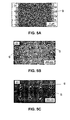
- FIGS 5A to 5C illustrate top view SEM images of arrays of CNTs grown according to specific embodiments of the invention.
- the present invention relates to a method for providing catalyst nanoparticles on a substrate.
- the method comprises in a first step forming at predetermined locations in the substrate holes or recesses having a bottom.
- the recesses also called holes or openings, are formed from a substrate surface into the substrate, and the bottom is located at that side of the recess furthest away from the substrate surface where the recess is formed.
- the terms recess, hole or opening hereinafter are intended to mean the same thing.
- providing nanoparticles onto the substrate may be performed by providing at least one layer of catalyst material onto the substrate such that the catalyst material at least covers the bottom of the recesses. Then, the at least one layer of catalyst material is broken up into nanoparticles. This may be done by using thermal and/or plasma assisted methods. For example breaking up the layer of catalyst material may be done by annealing the substrate (see further).
- providing nanoparticles onto the substrate may be performed by depositing the nanoparticles from a solution comprising the nanoparticles and a solvent. Depositing the nanoparticles onto the substrate may, for example, be done by spinning on the solution. After deposition of the nanoparticles onto the substrate, the solvent may be removed from the solution by e.g. evaporation during a thermal drying step such that only the nanoparticles remain on the substrate.
- nanoparticles provided or formed at locations different from the bottom of the recesses, e.g. at the substrate surface in between two recesses, are selectively removed.
- the present invention thus provides a method to create and isolate nanoparticles with narrow size distribution in predefined locations in a substrate.
- the narrow size distribution can be expressed as a size distribution having a variation in size or diameter between 5 and 10% or wherein the variation in diameter or size of the nanoparticles is within 5 and 10%, preferably between 5 and 8% (see further).
- the material of the nano-particles depends on the catalyst material used.
- the nanoparticles may preferably be metal-containing nanoparticles.
- the selectively deposited nanoparticles may be pure metal nanoparticles.
- the selectively deposited nanoparticles may be metal-silicide containing nanoparticles.
- the selectively deposited nanoparticles may be metal alloys.
- An advantage of the method for forming catalyst nanoparticles on a substrate according to embodiments of the invention is that it can be used with any size of substrate. Furthermore, it is fully compatible with existing semiconductor processing, e.g. for manufacturing nano-devices.
- the catalyst nanoparticles formed by the method for providing catalyst nanoparticles on a substrate according to embodiments of the invention may advantageously be used as a catalyst for growing elongate nanostructures.
- These nanoparticles deposited at predetermined locations on the substrate can catalyse the nucleation and growth of elongate nanostructures, e.g. carbon nanotubes (CNTs) or nanowires (NWs).
- CNTs carbon nanotubes
- NWs nanowires
- elongate nanostructures e.g. CNTs or NWs
- selectiveively deposited CNTs or NWs with control over diameter and length as well as location can be achieved (through growth) using said nanoparticles as catalyst.
- standard arrays of recesses may be used as templates for catalyst placement and CNT (NW) are grown inside the holes using e.g. Chemical Vapor Deposition (CVD) techniques.
- CVD Chemical Vapor Deposition
- standard array of recesses is meant that the array of recesses is formed using standard semiconductor processes of lithography and dry etching.
- recesses may be formed having, for example, a diameter of between 50 nm and 500 nm, for example a diameter of 80 nm or 100 nm or 150 nm or 200 nm or 250 nm or 300 nm, with pitches of, for example, 1, 2 or 8 times the diameter.
- the aspect ratios of the recesses may, for example, be 1:6, 1:4, 1:3, 1:2.5 or 1:2.
- the present invention thus also provides a method for forming elongate nanostructures on a substrate.
- the method comprises in a first step forming recesses in the substrate at predetermined locations, the recesses having a bottom. The bottom is defined as that wall of the recess furthest away from the substrate surface in which the recess is made.
- Next at least one layer of catalyst material is provided onto the substrate such that the catalyst material at least covers the bottom of the recesses.
- the at least one layer of catalyst material is broken up into nanoparticles, e.g. by annealing the substrate. Thereafter, nanoparticles formed at locations different from the bottom of the recesses are selectively removed.
- elongate nanostructures e.g. CNTs or NWs, are grown in the recesses using the nanoparticles as a catalyst.
- the method for forming elongate nanostructures on a substrate according to embodiments of the invention can be used with any size of substrate and is fully compatible with semiconductor processing technology.
- elongate nanostructures any two-dimensionally confined pieces of solid material in the form of wires (nanowires), tubes (nanotubes), rods (nanorods) and similar elongated substantially cylindrical or polygonal nanostructures having a longitudinal axis.
- a cross-dimension of the elongate nanostructures preferably lies in the region of 1 to 500 nanometers.
- organic elongate nanostructures such as e.g. carbon nanotubes (CNTs), or inorganic elongate nanostructures, such as e.g. semiconducting nanowires (e.g. silicon nanowires) may be used.
- CNTs carbon nanotubes
- inorganic elongate nanostructures such as e.g. semiconducting nanowires (e.g. silicon nanowires) may be used.
- CNTs carbon nanotubes
- inorganic elongate nanostructures such as e.g. semiconducting nanowires (e.g
- base growth or “bottom up growth” of CNTs as used in this application refer to CNT growth having the catalyst nanoparticle attached to the substrate.
- tip growth or “top down growth” of CNTs as used in this application refer to CNT growth having the CNTs attached to the surface and the nanoparticle being on top of the CNTs.
- pure metal nanoparticles refers to nanoparticles made of pure metal or nanoparticles formed by annealing a pure metal film.
- metal-silicide nanoparticles refers to nanoparticles made of metal-silicides such as Ni-silicide, Co-silicide, Fe-silicide, Ti-silicide,....
- metal-containing nanoparticles refer to both metal nanoparticles and metal-silicide nanoparticles.
- alloy refers to a mixture containing two or more metallic elements or metallic and nonmetallic elements which are fused together during an anneal (heating) step and thus dissolving into each other to result in nanoparticles containing two or more metallic elements or metallic and nonmetallic elements.
- active catalyst nanoparticles refers to nanoparticles which are suitable to be used as a catalyst for CNT (or NW) growth.
- active is to be understood as being capable of growing/synthesizing/creating a carbon nanotube using the formed nanoparticles.
- the growth/synthesis/ creation of a carbon nanotube is a multi-step process of first receiving a carbon source, followed by cracking the carbon and subsequently growing the carbon nanotube.
- the term "aspect ratio” refers to the ratio of the height dimension to the width dimension of particular recesses.
- a recess which typically extends in a tubular form into a layer has a height and a diameter, and the aspect ratio would be the height of the tubular recess divided by the diameter.
- a method for providing catalyst nanoparticles on a substrate S.
- the term “substrate” may include any underlying material or materials that may be used, or upon which a device, a circuit or an epitaxial layer may be formed.
- this "substrate” may include a semiconductor substrate such as e.g. a doped silicon, a gallium arsenide (GaAs), a gallium arsenide phosphide (GaAsP), an indium phosphide (InP), a germanium (Ge), or a silicon germanium (SiGe) substrate.
- GaAs gallium arsenide
- GaAsP gallium arsenide phosphide
- InP indium phosphide
- Ge germanium
- SiGe silicon germanium
- the "substrate” may include for example, an insulating layer such as a SiO 2 or an Si 3 N 4 layer in addition to a semiconductor substrate portion.
- the term substrate also includes silicon-on-glass, silicon-on sapphire substrates.
- the term “substrate” is thus used to define generally the elements for layers that underlie a layer or portions of interest.
- the "substrate” may be any other base on which a layer is formed, for example a glass or metal layer.
- the substrate S may be a silicon substrate.
- the method comprises forming recesses 3 in the substrate S at predetermined locations.
- standard arrays having rows and columns of recesses 3 may be formed.
- recesses may be formed having, for example, a diameter of between 50 nm and 500 nm, for example a diameter of 80 nm or 100 nm or 150 nm or 200 nm or 250 nm or 300 nm, with pitches of, for example, 1, 2 or 8 times the diameter.
- the aspect ratios of the recesses may, for example, be 1:6, 1:4, 1:3, 1:2.5 or 1:2.
- the standard arrays of recesses 3 can be formed directly in the substrate S, but more preferred the standard arrays of recesses 3 may be formed in a dielectric layer 2 deposited onto a base substrate 1, the dielectric layer 2 and the base substrate 1 together forming the substrate S.
- the dielectric layer 2 can be a SiO 2 layer which may, for example, be formed by thermally annealing a Si substrate or alternatively by depositing a SiO 2 layer e.g. by deposition techniques such as Chemically Vapor Deposition (CVD).
- CVD Chemically Vapor Deposition
- the dielectric layer 2 may be a low-k dielectric layer such as CVD deposited SiCO(H) material, zeolites, NCS or (suitable) organic low-k materials.
- the thickness t of the dielectric layer 2 is dependent on the application and may, for example, be in the range of between 100 nm and 1000 nm.
- the substrate S may comprise a base substrate 1, e.g. a semiconductor layer, with on top a dielectric layer 2 as described above.
- the base substrate 1 may comprise silicon.
- Figure 1A illustrates the formation of recesses 3 in said substrate S.
- recesses 3 may be formed in the dielectric layer 2 present on the base substrate 1.
- the recesses 3 may lithographically be defined using standard lithographic processing followed by standard dry oxide etching such as e.g. reactive ion etching to form the recesses 3 in the substrate S.
- Standard lithographic processing may at least comprise depositing at least one photosensitive layer, for example a photoresist layer and optionally an antireflective coating, onto the dielectric layer 2 and developing the photosensitive layers to create a photolithographic pattern.
- the photolithographic pattern may then be used as a mask in e.g. reactive ion etching to form recesses 3 in the dielectric layer 2.
- the diameters do of the recesses 3 may depend on the application.
- the diameters do of the recesses 3 may be between 50 nm and 500 nm and may, for example, be 80 nm, 100 nm or 150 nm or 200 nm or 250 nm or 300 nm.
- the depth d of the recesses 3 may depend on the application and on the thickness t of the dielectric layer 2 if one is present. For example, the depth d can be smaller than the thickness t of the dielectric layer 2 in case the recesses 3 are created into the dielectric layer 2 and contact between catalyst particles to be formed (see further) and the base substrate 1 underneath the dielectric layer 2 needs to be avoided.
- the depth d can be higher than the thickness t of the dielectric layer in case the recesses 3 are created into the dielectric layer 2 and contact to the base substrate 1 underneath is required, desired or allowed.
- the depth d of the recesses 3 may, for example, be in the range of between 500 nm and 1000 nm but is not limited hereto.
- the substrate S may only comprise a base substrate 1 without a dielectric layer 2 on top of this base substrate 1.
- recesses 3 may be provided in the base substrate 1 of the substrate S.
- the recesses 3 may be provided in dense, semi-dense or isolated arrays. Dense arrays typically may have a pitch of 1, semi-dense arrays may typically have a pitch of 1:2 and isolated arrays may typically have a pitch of 1:8. With pitch is meant the distance between neighbouring recesses 3.
- the aspect ratio of the recesses 3 may, for example, be 1:6, 1:4, 1:3, 1:2.5 or 1:2.
- nanoparticles are provided onto the substrate.
- providing nanoparticles may be provided by depositing at least one layer 4 of catalyst material onto the substrate S.
- Figure 1B illustrates the deposition of a layer 4 of catalyst material onto the dielectric layer 2 of the substrate S. It can be seen from the figure that, according to the present embodiment, the layer 4 of catalyst material is provided on a top surface of the dielectric layer 2 and on a bottom and side walls of the recesses 3. It has to be noted that, contrary to the example given in Figure 1B , the layer 4 of catalyst material may also only be provided at the bottom of the recesses 3. It is to be noted that, in the latter case, also catalyst material will end up on the surface of the substrate S.
- the at least one layer 4 of catalyst material may preferably be a metal-containing layer. At least one of the at least one layer 4 of catalyst material may be a metal-containing layer 4.
- the thickness of the at least one layer 4 of catalyst material may be lower than 20 nm and may more preferably be between 1 nm and 10 nm.
- the layer 4 of catalyst material may have a thickness of 2 nm, 5 nm, 8 nm, 9 nm or 10 nm.
- the thickness of the layer 4 of catalyst material may be lower than 1 nm, which may lead to small nanoparticles with a diameter in the range of between 0.2 nm and 0.5 nm.
- the layer 4 of catalyst material can be discontinuous on the top surface of the dielectric layer 2. Depending on the thickness of the layer 4, it can have different thicknesses inside the recesses 3. Most of the layer 4 of catalyst material inside the recesses 3 is located at the bottom of the recesses 3, especially when the layer 4 of catalyst material has a thickness lower than 8 nm.
- the layer 4 of catalyst material may comprise a material that, when heated up, leads to formation of active catalyst nanoparticles.
- the layer 4 of catalyst material may preferably comprise a metal and may according to most preferred embodiments comprise pure metal such as e.g. Co, Ti, Pt, W, Ni or Fe.
- the pure metal layer may be deposited using sputter techniques such as Physical Vapor Deposition (PVD) or deposition techniques such as Atomic Layer Deposition (ALD) or Chemical Vapor Deposition (CVD).
- the layer 4 of catalyst material may comprise a combination of a plurality of layers, for example, two layers, preferably two layers formed of metal such as e.g. Co, Ti, Pt, W, Ni or Fe.
- the two layers of metal may be deposited using sputter techniques such as Physical Vapor Deposition (PVD) or deposition techniques such as Atomic Layer Deposition (ALD) or Chemical Vapor Deposition (CVD).
- PVD Physical Vapor Deposition
- ALD Atomic Layer Deposition
- CVD Chemical Vapor Deposition
- the combination of two or more layers can also be a combination of at least one pure metal layer and at least one non-pure metal layer and/or at least one non-metal layer.
- the layer 4 of catalyst material may comprise a metal alloy.
- the substrate S comprises silicon and the layer 4 of catalyst material is a metal or metal alloy containing layer.
- the layer 4 of catalyst material is a metal or metal alloy containing layer.
- an intermediate barrier layer may be provided in between the substrate S and the layer 4 of catalyst material.
- the barrier layer may, for example, be Si 3 N 4 , TiN, TaN, HfN, SiO 2 , Si 3 N 4 , ... and may, for example, have a thickness of between 50 nm and 100 nm.
- the layer 4 of catalyst material may comprise a metal-silicide.
- a layer of silicon and a layer of metal may be deposited on the substrate S.
- a layer of silicon may be deposited onto the substrate S before the metal layer is deposited.
- the silicon layer may be deposited using CVD.
- the metal layer for forming the metal-silicide may preferably be Co, Ni, Ti, W, Pt or Fe.
- the metal layer may be deposited using PVD, ALD or CVD.
- the substrate S is a silicon substrate (e.g.
- a barrier layer may be deposited onto the base substrate 1 before depositing the silicon layer in order to avoid migration of metal-silicide nanoparticles into the base substrate 1.
- the barrier layer may, for example, be Si 3 N 4 , TiN, TaN, HfN, SiO 2 , Si 3 N 4 , ... and may, for example, have a thickness of between 50 nm and 100 nm.
- Figure 1C illustrates transformation of the at least one layer 4 of catalyst material into nanoparticles 5, 6 by thermal and/or plasma assisted methods, e.g. by performing an annealing or heating step on the substrate S.
- Annealing the substrate S may be performed by, for example, a Rapid Thermal Anneal (RTA) at a temperature in the range of between 500°C and 900°C, preferably between 600°C and 800°C.
- RTA Rapid Thermal Anneal
- the temperature at which annealing is performed may depend on the thickness of the layer 4 of catalyst material from which the nanoparticles 5, 6 have to be formed.
- annealing the substrate S may be performed for a time period of at least one minute up to a few minutes.
- the annealing may be performed under an N 2 atmosphere.
- the annealing may preferably be performed under vacuum circumstances without breaking the vacuum during annealing.
- the stress achieved in the layer 4 of catalyst material during the annealing process gives rise to the formation of two-dimensional islands or nanoparticles 5, 6 in horizontal areas, as is illustrated in Figure 1C .
- the thickness of the layer 4 of catalyst material as well as the temperature and time duration of the annealing step may have influence in controlling the size and more particularly the diameter of the nanoparticles 5, 6.
- thinner layers 4 may be transformed into smaller nanoparticles 5 with an increasing number density.
- the optimal temperature and time to create nanoparticles 5 may depend on the type of catalyst material used and the thickness of the layer 4 of the catalyst material.
- the required temperature at which annealing is performed depends on the thickness of the layer 4 of catalyst material and on the catalyst material used. In contrast, variation in the density of the arrays, i.e. the distance between neighbouring recesses 3, is found to have no significant impact on the formation of the nanoparticles 5, 6.
- Figure 2A shows a top view Scanning Electron Microscopy (SEM) picture of nanoparticles 5 formed at the bottom of the recesses 3 and nanoparticles 6 formed at the substrate surface, after an annealing step at 700°C for 1 minute in case where the catalyst material comprises Nickel.
- the layer 4 of catalyst material had a thickness of 2 mm. From this picture it can be seen that nanoparticles 6 are also formed at locations different from the bottom of the recesses 3, i.e. at the substrate surface. In the further description these nanoparticles 6 will be referred to as exterior nanoparticles 6.
- nanoparticles 5, 6 may be provided onto the substrate S by depositing the nanoparticles 5, 6 from a solution comprising the nanoparticles 5, 6 and a solvent. Deposition of the nanoparticles 5, 6 may preferably be done by spinning on of the solution to the substrate S.
- the nanoparticle 5, 6 may be formed by any suitable method known by a person skilled in the art, and may then be mixed with a solvent in order to be able to spin it on the substrate S. After deposition of the nanoparticles 5, 6 the solvent may be removed such that only the nanoparticles 5, 6 remain at the bottom of the recesses 3 and at the surface of the substrate S. Removing the solvent may, for example, be done by evaporating the solvent during a thermal drying step.
- the exterior nanoparticles 6 formed at locations different from the bottom of the recesses 3 may be selectively removed. Selectively removing of these exterior nanoparticles 6 may, for example, be performed as illustrated in Figure 1D .
- the recesses 3 may at least partly be filled with a sacrificial material 7, hereby at least covering the nanoparticles 5 present at the bottom of the recesses 3.
- At least partly filling the recesses 3 with sacrificial material 7 may, fore example, be done by spin-on techniques.
- the sacrificial material 7 may be an organic material, preferably a commercially available organic material, and may preferably be an organic polymeric material such as e.g. photolithographic materials such as a resist.
- At least partly filling the recesses 3 with sacrificial material 7 may be performed by depositing a sacrificial spin-on organic polymer 7 onto the substrate S such that at least the nanoparticles 5 in the recesses 3 are covered with the sacrificial spin-on organic polymer 7.
- the recesses 3 may be completely filled with sacrificial material 7. This may preferably be performed by spinning on at a predetermined rotational speed, e.g. at 2000 rpm, for a predetermined time, e.g. one or two minutes. However, according to other embodiments, only part of the recesses 3 may be filled with sacrificial material 7. This may also preferably be done by spinning on, but in this case less sacrificial material is to be used because only partial filling of the recesses 3 is required.
- the recesses 3 may be filled with sacrificial material 7 for one half or one third of the recesses 3, as long as the nanoparticles 5 formed on the bottom of the recesses 3 are covered with the sacrificial material 7.
- the step of at least partly filling the recesses 3 and thereby covering the nanoparticles 5 present at the bottom of the recesses 3 is mainly performed to protect the nanoparticles 5 at the bottom of the recesses 3 during further processing, more particularly during selective removal of the exterior nanoparticles 6 at locations different from the bottom of the recesses 3.
- Removing the exterior nanoparticles 6 may preferably be done by Chemical Mechanical Polishing (CMP).
- CMP Chemical Mechanical Polishing
- this step also protects the nanoparticles 5 formed at the bottom of the recesses 3 from external post-processing residues which could lead to unwanted contamination.
- the sacrificial material 7 may be removed. This may be done by a cleaning step which may be for example be a standard wet cleaning process suitable for removing the sacrificial material 7 without damaging the material of the substrate S. This cleaning step removes the sacrificial material 7 from the recesses 3, thereby releasing the nanoparticles 5 formed at the bottom of the recesses 3.
- an additional cleaning step such as e.g. a wet etch, may be performed to remove these impurities 8.
- the wet etch may, for example, comprise immersing the substrate S in a solution comprising H 2 SO 4 : H 2 O 2 in a volume ratio of e.g.
- FIG. 1 4 for, for example, five minutes at room temperature, also referred to as piranha etching.
- Figure 1E schematically illustrates the substrate S after the CMP process through which exterior nanoparticles have been removed, and a subsequent cleaning process as described above.
- Figure 2C shows a top view SEM picture of a substrate S after piranha etching at room temperature for five minutes. From this SEM picture it can be seen that the impurities 8 have been removed.
- the number of nanoparticles 5 formed at the bottom of one recess 3 depends on the size of the nanoparticles 5 formed and on the diameter d o of the recess 3.
- the number of nanoparticles 5 formed in a recess 3 is illustrated in Figure 3A for a recess 3 having a diameter of 100 nm.
- Figure 3A shows a histogram for the number of nanoparticles 5 formed per recess 3 after annealing of a 2 nm thick Ni catalyst layer at 700°C for 1 min. for recesses 3 having a diameter of 100 nm.
- the average number of nanoparticles 5 within the recesses may be 20 +/- 0.51.
- FIG. 3B illustrates a histogram of the size or diameter of nanoparticles 5 formed after annealing of a 2 nm thick Ni catalyst layer at 700°C for 1 min. in recesses 3 with a diameter of 100 nm.
- nanoparticles 5 can be formed with a narrow size distribution.
- the narrow size distribution can thus be expressed as a size or diameter distribution having a variation of between 5 and 10%, preferably between 5 and 8% or wherein the variation in diameter sizes of the nanoparticles is within 5 to 10%, preferably within 5 and 8%.
- the catalyst nanoparticles 5 formed at predetermined locations on a substrate S according to embodiments of the present invention may advantageously be used for growing CNTs, or in general elongate nanostructures, at the predetermined locations.
- the present invention also provides a method for forming elongate nanostructures on a substrate S.
- the method comprises providing catalyst nanoparticles at predetermined locations on a substrate S as described hereabove in embodiments of the present invention and subsequently growing elongate nanostructures in the recesses 3 using the nanoparticles 5 as a catalyst.
- Figure 1F illustrates growth of CNTs 9 using the nanoparticles 5 formed at the bottom of the recesses 3 as a catalyst. This may be done by exposing the nanoparticles to proper CNT synthesis conditions.
- the CNTs 9 may preferably be grown by Chemical Vapor Deposition (CVD) or Plasma Enhanced-CVD (PE-CVD). These methods use a carbon source such as e.g.
- the method for growing the CNTs 9 may use C 2 H 4 as a carbon source and gases such as N 2 and/or H 2 as assistant gases and may be performed at temperatures lower than 900°C, e.g. between 600°C and 800°C, as growth temperature.
- other carbon sources may be used, such as CH 4 , and other growth temperatures may be required.
- the growth temperature may be lower than 450°C to avoid damage to material of the substrate S on which the CNTs 9 are grown.
- growth temperatures lower than 500°C may also be suitable for growing CNTs 9.
- the diameter of the formed CNTs 9 may be consistent with, i.e. may be substantially the same as, the diameter of the original catalyst nanoparticles 5. With decreasing nanoparticle sizes, the diameter of the CNTs 9 may become smaller, following a one to one relation. Massive growth of CNTs 9 occurs for pure metal nanoparticles 5 up to 800°C.
- Figure 4A illustrates a histogram of the number of CNTs 9 grown from nanoparticles 5 formed after annealing of a 2 nm thick Ni catalyst layer at 700°C for 1 min. in recesses 3 having a diameter of 100 nm.
- the CNTs 9 are grown at 700°C and at a constant ethylene flow of 200 ml/min. for 1 min.
- the average number of CNTs 9 formed within the recesses 3 may for example be 20 CNTs per recess 3.
- Figure 4D shows a histogram for the diameter of the CNTs 9 grown from nanoparticles 5 formed after annealing of a 2 nm thick Ni catalyst layer at 700°C for 1 min. in recesses 3 having a diameter of 100 nm.
- the CNTs 9 are grown at 700°C and at a constant ethylene flow of 200 ml/min. for 1 min. From Figure 4B it can be seen that the mean CNT diameter is 12.5 nm.
- CNTs 9 may, according to embodiments, be grown by base growth or bottom up growth or may, according to other embodiments, be grown by tip growth or top down growth, depending on the interaction of the catalyst material with the substrate S. For example, no interaction or a weak interaction of the catalyst material with the substrate S may lead to tip growth resulting in a CNT 9 with the nanoparticle 5 on top..
- the properties of the resulting CNTs 9 may depend on the process parameters used during growth of the CNTs 9. For example, the resulting CNTs 9 may be straighter when the growth temperature is increased. Furthermore, at growth temperatures of 900°C only a few nanoparticles 5 can catalyze CNT growth. This effect is attributed to poisoning of the catalyst nanoparticles 5. Because of the high temperature, C 2 H 4 decomposes faster than carbon diffuses into the catalyst nanoparticles 5. Hence, the catalyst particles 5 become covered with amorphous carbon and cannot catalyse CNT growth anymore.
- the CNTs 9 can easily be released from the substrate S after growth if this would be required. This may, for example in case of low interaction between the CNT 9 and the substrate S, be done by rinsing with e.g. deionized water.
- the method of the preferred embodiments for growing CNTs 9 based on the method according to embodiments of the invention can, for example, be used for manufacturing semiconductor devices.
- tip growth or top down growth of CNTs 9, i.e. when the nanoparticles 5 are attached to the top of the CNTs 9, makes it easy to realize electrical contacts to the grown CNT 9.
- a Ni layer 4 was deposited using Physical Vapor Deposition (PVD) and the layer 4 was annealed at a temperature of 700°C for 1 minute.
- the nanoparticle size distribution was determined by SEM characterization. Under the mentioned annealing conditions, the particle diameter of the nanoparticles 5, 6 originating from the 8 nm thick deposited Ni layer was 67 nm ⁇ 6 nm. The particle diameter of the nanoparticles 5, 6 originating from the 2 nm thick deposited Ni layer was 17 nm ⁇ 4 nm.
- the diameter of the nanoparticles 5, 6 depends on the thickness of the layer 4 of catalyst material, in the example given the thickness of the metal, i.e. Ni or Co, layer 4.
- Example 2 Growth of CNTs using Co and Ni nanoparticles as a catalyst
- the Ni and Co nanoparticles 5 were exposed to a wide range of synthesis conditions.
- a CVD chamber was used for performing CNT growth.
- the system may comprise a load-lock pre-chamber from which samples can be transferred, using a magnetic transfer rod, to a fixed bed reactor comprising an 80 mm diameter quartz tube, 120 cm in length and surrounded by a horizontal furnace.
- the pressure of the system can be varied from atmospheric pressure to 1 mbar, whereas the temperature can reach 1200°C.
- a carbon source, hydrogen and nitrogen gases are supplied directly to the fixed bed reactor at flow rates ranging from 100 to 5000 ml/min and a maximum pressure of 3 bar. All samples were preconditioned at the desired growth temperature. Each sample was placed in the centre of the reactor under a constant flow of carrier gases, in the example given a mix of N 2 and H 2 , with flow rates of respectively 4000 ml/min and 2000 ml/min, for 2 minutes. Subsequently, ethylene was released into the furnace at different flow rates of 100ml/min, 200ml/min and 500ml/min. CNT growth was done under atmospheric pressure at several temperatures ranging from 600°C to 800°C and for different periods of time, i.e. for 1, 2, 5 and 10 minutes.
- long CNTs 9 with a length up to 15 ⁇ m may be obtained.
- the CNTs 9 obtained under these circumstances are entangled and may cover the whole array area on the surface of the substrate S, also outside the recesses 3, as is shown in Figure 5A .
- the CNTs 9 grow out of the recesses 3 and can then entangle with neighbouring CNTs 9 growing in the same recess 3 and even with CNTs 9 growing in neighbouring recesses 3.
- CNT growth was performed at shorter growth times, while keeping the rest of the growth parameters constant with respect to the above-described CNT growth process.
- the length of the CNTs 9 may be tailored hereby avoiding entanglement when CNTs 9 grow outside, i.e. above, the recess 3 as was the case in the above-described growth process which was illustrated in Figure 5A .
- CNTs 9 are grown from the inside of the recesses 3 in bundles. This is due to the formation of several nanoparticles 5 per recess 3. In general, the 1-to-1 nanoparticle/nanotube ratio may easily be achieved. Uniformity in growth density, i.e. of the amount of CNTs 9 in one recess 3, in a same array of recesses 3 was observed, which indicates that the deposition of the layer 4 of catalyst material according to embodiments of the invention may be uniform.
- catalytic activity of the selectively deposited nanoparticles 5 according to embodiments of the invention is comparable with that observed from blanket films, i.e. no loss in catalytic activity is observed by depositing it into the recesses 3 in the substrate S.
- the CNT diameter distribution is also observed to be uniform. Closer SEM inspection reveals that tube diameters vary accordingly with that of the nanoparticle from which it is grown, following a one to one relation, as is widely reported. This supports the fact that precise control of the CNT diameter is mainly limited by the size of the catalyst nanoparticles 5 from which the CNTs 9 are grown.
- This phenomenon may take, for example, place in case the substrate S comprises a base substrate 1 and a SiO 2 layer 2 on top of the base substrate 1, since the nanoparticles 5 do not adhere to the SiO 2 layer 2 on which they are formed. As a consequence, as-grown CNTs 9 tend to easily lift off from the substrate S. This phenomenon is especially observed for long periods of growth times due to CNT entanglement. Overall, all features described above were observed in the centre as well as in edge areas of the substrate S. Moreover, Ni and Co nanoparticles 5 did not show any difference in terms of catalytic behavior.
Landscapes
- Chemical & Material Sciences (AREA)
- Engineering & Computer Science (AREA)
- Materials Engineering (AREA)
- Nanotechnology (AREA)
- Organic Chemistry (AREA)
- Physics & Mathematics (AREA)
- Chemical Kinetics & Catalysis (AREA)
- General Physics & Mathematics (AREA)
- Condensed Matter Physics & Semiconductors (AREA)
- Computer Hardware Design (AREA)
- Microelectronics & Electronic Packaging (AREA)
- Power Engineering (AREA)
- Manufacturing & Machinery (AREA)
- Crystallography & Structural Chemistry (AREA)
- Composite Materials (AREA)
- Thermal Sciences (AREA)
- Inorganic Chemistry (AREA)
- Catalysts (AREA)
- Carbon And Carbon Compounds (AREA)
Priority Applications (2)
| Application Number | Priority Date | Filing Date | Title |
|---|---|---|---|
| US11/935,998 US20090131245A1 (en) | 2006-12-21 | 2007-11-06 | Controlled and selective formation of catalyst nanaoparticles |
| JP2007328744A JP5329800B2 (ja) | 2006-12-21 | 2007-12-20 | 触媒ナノ粒子の制御および選択的な形成 |
Applications Claiming Priority (1)
| Application Number | Priority Date | Filing Date | Title |
|---|---|---|---|
| US87623406P | 2006-12-21 | 2006-12-21 |
Publications (1)
| Publication Number | Publication Date |
|---|---|
| EP1946833A1 true EP1946833A1 (fr) | 2008-07-23 |
Family
ID=38236488
Family Applications (1)
| Application Number | Title | Priority Date | Filing Date |
|---|---|---|---|
| EP07006228A Withdrawn EP1946833A1 (fr) | 2006-12-21 | 2007-03-27 | Nanoparticules de catalyseur pour l'obtention de nanotubes de carbone |
Country Status (3)
| Country | Link |
|---|---|
| US (1) | US20090131245A1 (fr) |
| EP (1) | EP1946833A1 (fr) |
| JP (1) | JP5329800B2 (fr) |
Cited By (2)
| Publication number | Priority date | Publication date | Assignee | Title |
|---|---|---|---|---|
| EP2221877A2 (fr) * | 2009-02-18 | 2010-08-25 | Korea Institute Of Industrial Technology | Procédé de fabrication de nanofils en silicone, cellule solaire incluant les nanofils en silicone et procédé de fabrication de la cellule solaire |
| WO2010108957A1 (fr) * | 2009-03-27 | 2010-09-30 | Commissariat A L'energie Atomique Et Aux Energies Alternatives | Procédé de réalisation d'interconnexions électriques a nanotubes de carbone |
Families Citing this family (12)
| Publication number | Priority date | Publication date | Assignee | Title |
|---|---|---|---|---|
| US7736979B2 (en) * | 2007-06-20 | 2010-06-15 | New Jersey Institute Of Technology | Method of forming nanotube vertical field effect transistor |
| US8668833B2 (en) * | 2008-05-21 | 2014-03-11 | Globalfoundries Singapore Pte. Ltd. | Method of forming a nanostructure |
| JP2011178631A (ja) * | 2010-03-02 | 2011-09-15 | Nagoya Univ | カーボンナノチューブの製造方法,カーボンナノチューブ製造用の単結晶基板,およびカーボンナノチューブ |
| JP5660804B2 (ja) | 2010-04-30 | 2015-01-28 | 東京エレクトロン株式会社 | カーボンナノチューブの形成方法及びカーボンナノチューブ成膜装置 |
| KR101414096B1 (ko) * | 2011-11-28 | 2014-07-02 | 한국과학기술연구원 | 유연성 소자용 부재 및 그 제조방법 |
| WO2015123461A1 (fr) * | 2014-02-12 | 2015-08-20 | California Institute Of Technology | Nanostructures d'or refondu pour la spectroscopie raman renforcée en surface |
| US9987609B2 (en) | 2014-09-05 | 2018-06-05 | California Institute Of Technology | Multiplexed surface enhanced Raman sensors for early disease detection and in-situ bacterial monitoring |
| US9512000B2 (en) | 2014-12-09 | 2016-12-06 | California Institute Of Technology | Fabrication and self-aligned local functionalization of nanocups and various plasmonic nanostructures on flexible substrates for implantable and sensing applications |
| KR102251999B1 (ko) | 2015-01-09 | 2021-05-17 | 삼성전자주식회사 | 펠리클 및 이의 제조 방법 |
| KR101798283B1 (ko) | 2015-06-08 | 2017-11-16 | 단국대학교 산학협력단 | 탄소 나노튜브의 수직 성장을 위한 촉매의 증착 방법 |
| US10501851B2 (en) * | 2016-05-12 | 2019-12-10 | Fei Company | Attachment of nano-objects to beam-deposited structures |
| US9859157B1 (en) | 2016-07-14 | 2018-01-02 | International Business Machines Corporation | Method for forming improved liner layer and semiconductor device including the same |
Citations (2)
| Publication number | Priority date | Publication date | Assignee | Title |
|---|---|---|---|---|
| US20040131795A1 (en) * | 2002-12-27 | 2004-07-08 | National Chiao Tung University | Method to control the magnetic alloy-encapsulated carbon-base nanostructures |
| US20050133476A1 (en) * | 2003-12-17 | 2005-06-23 | Islam M. S. | Methods of bridging lateral nanowires and device using same |
Family Cites Families (4)
| Publication number | Priority date | Publication date | Assignee | Title |
|---|---|---|---|---|
| US7115305B2 (en) * | 2002-02-01 | 2006-10-03 | California Institute Of Technology | Method of producing regular arrays of nano-scale objects using nano-structured block-copolymeric materials |
| JP3869394B2 (ja) * | 2003-06-30 | 2007-01-17 | 富士通株式会社 | 微粒子の堆積方法及びカーボンナノチューブの形成方法 |
| US20070084346A1 (en) * | 2005-09-30 | 2007-04-19 | Paul Boyle | Nanostructures containing carbon nanotubes and methods of their synthesis and use |
| WO2007074506A1 (fr) * | 2005-12-26 | 2007-07-05 | Fujitsu Limited | Procédé de croissance de nanotube de carbone et système de croissance de nanotube de carbone |
-
2007
- 2007-03-27 EP EP07006228A patent/EP1946833A1/fr not_active Withdrawn
- 2007-11-06 US US11/935,998 patent/US20090131245A1/en not_active Abandoned
- 2007-12-20 JP JP2007328744A patent/JP5329800B2/ja not_active Expired - Fee Related
Patent Citations (2)
| Publication number | Priority date | Publication date | Assignee | Title |
|---|---|---|---|---|
| US20040131795A1 (en) * | 2002-12-27 | 2004-07-08 | National Chiao Tung University | Method to control the magnetic alloy-encapsulated carbon-base nanostructures |
| US20050133476A1 (en) * | 2003-12-17 | 2005-06-23 | Islam M. S. | Methods of bridging lateral nanowires and device using same |
Cited By (5)
| Publication number | Priority date | Publication date | Assignee | Title |
|---|---|---|---|---|
| EP2221877A2 (fr) * | 2009-02-18 | 2010-08-25 | Korea Institute Of Industrial Technology | Procédé de fabrication de nanofils en silicone, cellule solaire incluant les nanofils en silicone et procédé de fabrication de la cellule solaire |
| EP2221877A3 (fr) * | 2009-02-18 | 2014-12-17 | Korea Institute Of Industrial Technology | Procédé de fabrication de nanofils en silicone, cellule solaire incluant les nanofils en silicone et procédé de fabrication de la cellule solaire |
| WO2010108957A1 (fr) * | 2009-03-27 | 2010-09-30 | Commissariat A L'energie Atomique Et Aux Energies Alternatives | Procédé de réalisation d'interconnexions électriques a nanotubes de carbone |
| FR2943850A1 (fr) * | 2009-03-27 | 2010-10-01 | Commissariat Energie Atomique | Procede de realisation d'interconnexions electriques a nanotubes de carbone |
| US8518816B2 (en) | 2009-03-27 | 2013-08-27 | Commissariat A L'energie Atomique Et Aux Energies Alternatives | Method for making electrical interconnections with carbon nanotubes |
Also Published As
| Publication number | Publication date |
|---|---|
| JP5329800B2 (ja) | 2013-10-30 |
| JP2009155111A (ja) | 2009-07-16 |
| US20090131245A1 (en) | 2009-05-21 |
Similar Documents
| Publication | Publication Date | Title |
|---|---|---|
| EP1946833A1 (fr) | Nanoparticules de catalyseur pour l'obtention de nanotubes de carbone | |
| EP2011572B1 (fr) | Procédé pour la formation de nanoparticules de catalyseur pour créer des nanostructures allongées | |
| KR100956832B1 (ko) | 미리 형성된 나노튜브를 사용하여 부직포 및 제품을 제조하는 방법 | |
| US8400053B2 (en) | Carbon nanotube films, layers, fabrics, ribbons, elements and articles | |
| JP5607693B2 (ja) | 基板上にナノ粒子を位置付けるための方法 | |
| JP5519936B2 (ja) | ナノ構造体に基づく相互接続および熱の散逸体 | |
| US8872154B2 (en) | Field effect transistor fabrication from carbon nanotubes | |
| US20100328898A1 (en) | Integrated Circuits Having Interconnects and Heat Dissipators Based on Nanostructures | |
| WO2004065655A1 (fr) | Procedes d'utilisation de couches metalliques minces pour former des nanotubes, des films, des couches, des tissus, des rubans, des elements et des articles de carbone | |
| WO2001018866A1 (fr) | Points et cretes atomiques a texture prononcee | |
| EP1590498A1 (fr) | Procedes de fabrication de films, couches, tissus, rubans, elements et articles de nanotubes de carbone | |
| JP2006297549A (ja) | 金属ナノ粒子の配列蒸着方法及び金属ナノ粒子を用いたカーボンナノチューブの成長方法 | |
| JP2007105822A (ja) | 原子スケール金属ワイヤもしくは金属ナノクラスター、およびこれらの製造方法 | |
| JP2007180546A (ja) | カーボンナノチューブの形成方法、及びそれを利用した半導体素子の配線形成方法 | |
| JP2010064951A (ja) | 単結晶半導体ナノワイヤの形成 | |
| TW202325648A (zh) | 一種選擇性蝕刻奈米結構之方法製成的奈米結構 | |
| US7814566B2 (en) | Tip array structure and fabricating method of tip structure | |
| US20060084570A1 (en) | System and method for growing nanostructures from a periphery of a catalyst layer | |
| US20100300728A1 (en) | Nanowires using a carbon nanotube template | |
| JP2004241572A (ja) | 半導体装置及びその製造方法 | |
| Esconjauregui et al. | Patterning of metallic nanoparticles for the growth of carbon nanotubes | |
| Li et al. | Silica Particle‐Mediated Growth of Single Crystal Graphene Ribbons on Cu (111) Foil | |
| KR101030434B1 (ko) | 탄소용융환원반응을 이용한 나노 홀 형성 방법 | |
| Li | The Kinetics of Dissolution of Single Crystal Diamond (100) and (110) in Nickel and Cobalt Films and Vapor-Liquid-Solid Growth of Graphene Ribbons on Single Crystal and Polycrystalline Cu Foils | |
| JPH113988A (ja) | 超微細突起構造体およびその製造方法 |
Legal Events
| Date | Code | Title | Description |
|---|---|---|---|
| PUAI | Public reference made under article 153(3) epc to a published international application that has entered the european phase |
Free format text: ORIGINAL CODE: 0009012 |
|
| 17P | Request for examination filed |
Effective date: 20071026 |
|
| AK | Designated contracting states |
Kind code of ref document: A1 Designated state(s): AT BE BG CH CY CZ DE DK EE ES FI FR GB GR HU IE IS IT LI LT LU LV MC MT NL PL PT RO SE SI SK TR |
|
| AX | Request for extension of the european patent |
Extension state: AL BA HR MK RS |
|
| AKX | Designation fees paid |
Designated state(s): AT BE BG CH CY CZ DE DK EE ES FI FR GB GR HU IE IS IT LI LT LU LV MC MT NL PL PT RO SE SI SK TR |
|
| RAP1 | Party data changed (applicant data changed or rights of an application transferred) |
Owner name: IMEC |
|
| 17Q | First examination report despatched |
Effective date: 20110406 |
|
| STAA | Information on the status of an ep patent application or granted ep patent |
Free format text: STATUS: EXAMINATION IS IN PROGRESS |
|
| STAA | Information on the status of an ep patent application or granted ep patent |
Free format text: STATUS: THE APPLICATION IS DEEMED TO BE WITHDRAWN |
|
| 18D | Application deemed to be withdrawn |
Effective date: 20161006 |