EP1946438B1 - Schaltung zur signalaufbereitung mit gemeinsamen oszillator - Google Patents
Schaltung zur signalaufbereitung mit gemeinsamen oszillator Download PDFInfo
- Publication number
- EP1946438B1 EP1946438B1 EP06828927.1A EP06828927A EP1946438B1 EP 1946438 B1 EP1946438 B1 EP 1946438B1 EP 06828927 A EP06828927 A EP 06828927A EP 1946438 B1 EP1946438 B1 EP 1946438B1
- Authority
- EP
- European Patent Office
- Prior art keywords
- signal
- stage
- oscillator
- mixer
- supplied
- Prior art date
- Legal status (The legal status is an assumption and is not a legal conclusion. Google has not performed a legal analysis and makes no representation as to the accuracy of the status listed.)
- Active
Links
Images

Classifications
-
- H—ELECTRICITY
- H03—ELECTRONIC CIRCUITRY
- H03C—MODULATION
- H03C3/00—Angle modulation
- H03C3/38—Angle modulation by converting amplitude modulation to angle modulation
- H03C3/40—Angle modulation by converting amplitude modulation to angle modulation using two signal paths the outputs of which have a predetermined phase difference and at least one output being amplitude-modulated
-
- H—ELECTRICITY
- H03—ELECTRONIC CIRCUITRY
- H03K—PULSE TECHNIQUE
- H03K3/00—Circuits for generating electric pulses; Monostable, bistable or multistable circuits
- H03K3/02—Generators characterised by the type of circuit or by the means used for producing pulses
- H03K3/023—Generators characterised by the type of circuit or by the means used for producing pulses by the use of differential amplifiers or comparators, with internal or external positive feedback
- H03K3/0231—Astable circuits
-
- H—ELECTRICITY
- H03—ELECTRONIC CIRCUITRY
- H03D—DEMODULATION OR TRANSFERENCE OF MODULATION FROM ONE CARRIER TO ANOTHER
- H03D7/00—Transference of modulation from one carrier to another, e.g. frequency-changing
- H03D7/16—Multiple-frequency-changing
-
- H—ELECTRICITY
- H03—ELECTRONIC CIRCUITRY
- H03D—DEMODULATION OR TRANSFERENCE OF MODULATION FROM ONE CARRIER TO ANOTHER
- H03D7/00—Transference of modulation from one carrier to another, e.g. frequency-changing
- H03D7/16—Multiple-frequency-changing
- H03D7/165—Multiple-frequency-changing at least two frequency changers being located in different paths, e.g. in two paths with carriers in quadrature
Definitions
- the invention relates to a circuit for signal processing in several stages with common oscillator for minimizing the noise.
- the signal / noise ratio is deteriorated at each stage.
- a major problem with this is that the oscillators assigned to the individual stages are realized independently of each other. Consequently, the phase fluctuations of the individual oscillators and clock generators are completely uncorrelated with each other, so that the total noise increases due to this lack of correlation.
- WO 03/007564 A shows a circuit for signal conditioning consisting of a first stage with a digital / analog converter and a second stage with an I / Q modulator out.
- From the GB 2 310 342 A also shows a multi-stage transmitter system, which has a mixer in a third stage.
- the object of the invention is to minimize the phase noise in a circuit for multi-stage signal processing.
- a single common oscillator is used in a multi-stage circuit for signal processing with a digital / analog converter, an I / Q modulator and at least one mixer instead of a multiplicity of oscillators for the individual stages.
- phase fluctuations are correlated with each other, so that the total noise decreases due to this correlation.
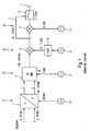
- the circuit arrangement in Fig. 1 comprises a plurality of signal processing stages, wherein the stages by a digital / analog converter 1, an I / Q modulator 2, the mixer 3 and 4, and a switch 5 are formed.
- the digital / analogue converter 1 is supplied with the in-phase (I) and quadrature (Q) components of a digital baseband signal via two supply lines.
- a clock signal is supplied, which is derived from a first oscillator 12.
- the converted analog signal is supplied to the inputs of an I / Q modulator 2 in its I and Q components.
- an oscillator signal is supplied, which is generated by the second oscillator 13.
- the I / Q modulated signal is fed to a first mixer 3 at its first input.
- a variable frequency signal from a synthesizer 10, such as a PLL (phased locked loop) is fed into the mixer 3, which is derived from a third oscillator 14 as a reference signal.
- the signal from the mixer 3 is fed to a first input of the mixer 4.
- a signal is fed, which is derived from a fourth oscillator 15.
- the output signal from the second mixer 4 is supplied to a changeover switch 6 at a first input.
- the output signal from the first mixer 3 is supplied to the switch 6 via a connection 5 at a second input.
- the switch 6 is connected to the output 7 of the signal conditioning circuit.
- the baseband signal fed to the digital-to-analog converter has a bandwidth of 0 to 40 MHz. This applies in each case to the I and Q channels of the baseband signal fed into the circuit for signal processing.
- the digital / analog converter 1 is supplied with a clock signal of 400 MHz.
- the analog I and Q channels at the output of the digital-to-analog converter 1 are respectively supplied to the I / Q modulator 2.
- the signal in the illustrated embodiment is in Fig. 3 a bandwidth between 60 and 140 MHz.
- the signal is at frequencies of 3.86 and 3.94 GHz.
- the thus modulated signal is mixed via a signal or frequency synthesizer 10 in the frequency range of 0.1 to 3.3 GHz.
- This signal can be connected via a line 5 and the switch 6 directly to the output 7.
- the mixer stage 4 is fed to an oscillator signal of a frequency of 6.4 GHz.
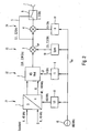
- FIG Fig. 2 A modified circuit arrangement according to the invention is shown in FIG Fig. 2 shown. This consists essentially of the same components as the circuit in Fig. 1 , The components have been provided with the same reference numerals for clarity.
- Fig. 2 In the circuit arrangement of Fig. 2 also find a digital / analog converter 1, an I / Q modulator 2, the mixer 3 and 4, the connection 5 and a switch 6. About the connection 5, the output signal of the mixer 3 also directly, via the switch 6, be given to the output 7.
- the circuit arrangement includes a frequency divider 8, frequency multiplier 9 and 11, as well as the frequency synthesizer 10.
- the interconnection of the components in Fig. 2 , as well as their function is essentially the same as in Fig. 1 , According to the invention, however, unlike the circuit according to the Fig. 3 the frequency divider 8, the frequency multipliers 9 and 11, as well as the frequency synthesizer 10 at their inputs, the signal supplied to only one common oscillator 16.
- FIGS. 3 and 4 explains the operation of an I / Q modulator and a frequency synthesizer.
- Fig. 3 shows a conventional I / Q modulator 2, which in Fig. 2 is used.
- the I and Q components of a complex baseband signal are converted via low-pass filters 30, 31, a pair of mixers 32, 33 and an adder 34 into an intermediate frequency position f IF .
- the I and Q components are low-pass filtered to eliminate possible harmonics or harmonics of the D / A converter 1.
- Fig. 4 shows a conventional frequency synthesizer 10, as in the circuit after Fig. 2 can be used.
- a phase comparator receives the reference frequency f osz as a first input signal . This reference frequency is compared with a signal from a variable frequency divider 43 with the partial factor 1 / n.
- a control signal is output, which is passed through the low-pass filter 41 integrally to the voltage-controlled oscillator, 42.
- the resonant frequency of the resonant circuit can be varied depending on the input voltage.
- the invention is not limited to the described embodiments.
- the circuit arrangement according to the invention for signal processing can be used in many ways.
Landscapes
- Engineering & Computer Science (AREA)
- Power Engineering (AREA)
- Amplitude Modulation (AREA)
- Transmitters (AREA)
- Digital Transmission Methods That Use Modulated Carrier Waves (AREA)
- Analogue/Digital Conversion (AREA)
- Stabilization Of Oscillater, Synchronisation, Frequency Synthesizers (AREA)
Description
- Die Erfindung betrifft eine Schaltung zur Signalaufbereitung in mehreren Stufen mit gemeinsamen Oszillator zur Minimierung des Rauschens.
- Bei der mehrstufigen Signalaufbereitung, beispielsweise bestehend aus einem Digital/Analog-Wandler, einem I/Q-Modulator und mehreren Mischern, wird das Signal/RauschVerhältnis an jeder Stufe verschlechtert. Ein wesentliches Problem dabei ist, dass die den einzelnen Stufen zugeordneten Oszillatoren unabhängig voneinander realisiert werden. Folglich sind die Phasenfluktuationen der einzelnen Oszillatoren und Taktgeneratoren völlig unkorreliert zueinander, so dass durch diese mangelnde Korrelation das Gesamtrauschen ansteigt.
- Aus der
WO 03/007564 A - Aus Der
GB 2 310 342 A - Aufgabe der Erfindung ist es, das Phasenrauschen in einer Schaltung zur mehrstufigen Signalaufbereitung zu minimieren.
- Die Aufgabe wird durch den einzigen Patentanspruch 1 gelöst.
- Erfindungsgemäß wird in einer mehrstufigen Schaltung zur Signalaufbereitung mit einem Digital/Analog-Wandler, einem I/Q-Modulator und zumindest einem Mischer statt einer Vielfachheit von Oszillatoren für die einzelnen Stufen ein einzelner gemeinsamer Oszillator verwendet.
- Damit sind die Phasenfluktuationen korreliert zueinander, so dass durch diese Korrelation das Gesamtrauschen absinkt.
- Anhand der Zeichnung wird nachfolgend ein Ausführungsbeispiel der Erfindung beschrieben. In der Zeichnung zeigen:
- Fig. 1
- eine Schaltungsanordnung zur mehrstufigen Signalaufbereitung gemäß dem Stand der Technik;
- Fig. 2
- eine Schaltungsanordnung zur mehrstufigen Signalaufbereitung gemäß der Erfindung;
- Fig. 3
- einen im Rahmen der Erfindung verwendbaren I/Q-Modulator und
- Fig. 4
- einen im Rahmen der Erfindung verwendbaren Frequenzsynthesizer.
- Die Schaltungsanordnung in
Fig. 1 gemäß dem Stand der Technik umfasst mehrere Signalverarbeitungsstufen, wobei die Stufen durch einen Digital/Analog-Wandler 1, einen I/Q-Modulator 2, die Mischer 3 und 4, sowie einen Umschalter 5 ausgebildet werden. - Dem Digital/Analog-Wandler 1 werden über zwei Zuleitungen die Inphase (I)- und Quadratur (Q)-Komponente eines digitalen Basisbandsignals zugeführt. An einem dritten Eingang wird dem Digital/Analog-Wandler 1 ein Taktsignal zugeführt, welches von einem ersten Oszillator 12 abgeleitet wird. Das gewandelte, analoge Signal wird in seinen I- und Q-Komponenten den Eingängen eines I/Q-Modulators 2 zugeführt. An einem dritten Eingang wird dem I/Q-Modulator 2 ein Oszillator-Signal zugeführt, welches von dem zweiten Oszillator 13 erzeugt wird.
- Das I/Q-modulierte Signal wird in einen ersten Mischer 3 an seinem ersten Eingang eingespeist. An einem zweiten Eingang wird in den Mischer 3 ein Signal mit variabler Frequenz aus einem Synthesizer 10, z.B. einer PLL (phaselocked-loop), eingespeist, welche von einem dritten Oszillator 14 als Referenzsignal abgeleitet ist. Das Signal aus dem Mischer 3 wird an einem ersten Eingang des Mischers 4 eingespeist. An einem zweiten Eingang des Mischers 4 wird ein Signal eingespeist, welche von einem vierten Oszillator 15 abgeleitet ist.
- Das Ausgangs-Signal aus dem zweiten Mischer 4 wird einem Umschalter 6 an einem ersten Eingang zugeführt. Das Ausgangs-Signal aus dem ersten Mischer 3 wird dem Umschalter 6 über eine Verbindung 5 an einem zweiten Eingang zugeführt. Der Umschalter 6 ist mit dem Ausgang 7 der Schaltung zur Signalaufbereitung verbunden.
- In der dargestellten Konfiguration weist das in den Digital/Analog-Wandler eingespeiste Basisbandsignal eine Bandbreite von 0 bis 40 MHz auf. Dies gilt jeweils für den I- und Q-Kanal des in die Schaltung zur Signalaufbereitung eingespeisten Basisbandsignals. Dem Digital/Analog-Wandler 1 wird ein Taktsignal von 400 MHz zugeführt.
- Die analogen I- und Q-Kanäle am Ausgang des Digital/Analog-Wandlers 1 werden jeweils dem I/Q-Modulator 2 zugeführt. Nach der Digital/Analog-Wandlung in der Stufe 21 besitzt das Signal in der dargestellten Ausführung in
Fig. 3 eine Bandbreite zwischen 60 und 140 MHz. Nach der I/Q-Modulation mit dem I/Q-Modulator 2 in der Stufe 22 und der gleichzeitigen Anhebung in den Zwischenfrequenzbereich von 4 GHz liegt das Signal um Frequenzen von 3,86 und 3,94 GHz. Mittels des ersten Mischers 3 in der ersten Mischerstufe 23 wird das so modulierte Signal über einen Signal- oder Frequenzsynthesizer 10 in den Frequenzbereich von 0,1 bis 3,3 GHz gemischt. Dieses Signal kann über eine Leitung 5 und den Umschalter 6 direkt mit dem Ausgang 7 verbunden werden. In einer weiteren Mischerstufe 24 mit dem zweiten Mischer 4 kann das Signal weiter umgesetzt werden. In der Darstellung wird der Mischerstufe 4 ein Oszillator-Signal einer Frequenz von 6,4 GHz zugeführt. - Eine veränderte Schaltungsanordnung gemäß der Erfindung ist in
Fig. 2 dargestellt. Dieses besteht im wesentlichen aus den gleichen Komponenten wie die Schaltung inFig. 1 . Die Komponenten wurden zur besseren Übersichtlichkeit mit der gleichen Bezugszeichen versehen. - In der Schaltungsanordnung der
Fig. 2 finden sich so ebenfalls ein Digital/Analog-Wandler 1, ein I/Q-Modulator 2, die Mischer 3 und 4, die Verbindung 5 sowie ein Umschalter 6. Über die Verbindung 5 kann das Ausgangssignal des Mischers 3 auch direkt, über den Umschalter 6, an den Ausgang 7 gegeben werden. - Die Schaltungsanordnung enthält einen Frequenzteiler 8, Frequenzvervielfacher 9 und 11, sowie den Frequenzsynthesizer 10. Die Verschaltung der Komponenten in
Fig. 2 , sowie deren Funktion ist im wesentlichen die gleiche wie inFig. 1 . Erfindungsgemäß wird jedoch im Unterschied zur Schaltung nach derFig. 3 dem Frequenzteiler 8, den Frequenzvervielfachern 9 und 11, sowie dem Frequenzsynthesizer 10 an deren Eingängen das Signal nur eines gemeinsamen Oszillators 16 zugeführt. - Durch die Nutzung dieses einzelnen Oszillators 16, dessen Signal den einzelnen Stufen 21-24 zugeführt wird, sind die Phasenfluktuationen der auftretenden Oszillatorsignale und somit auch der Ausgangs-Signale der einzelnen Stufen 21-24 korreliert, sodass durch die bestehende Korrelation das Gesamtrauschen der Schaltungsanordnung im Vergleich zu
Fig. 1 vermindert wird. Durch den Frequenzteiler 8 und die Frequenzvervielfacher 9 und 11 wird die Verwendung eines gemeinsamen Oszillatorsignals des Oszillators 16 ermöglicht. - Zum besseren Verständnis der Schaltungsanordnungen zur mehrstufigen Signalaufbereitung gemäß der Erfindung in
Fig. 2 werden nachfolgend anhand derFiguren 3 und 4 die Funktionsweise eines I/Q-Modulator und eines Frequenzsynthesizers erklärt. -
Fig. 3 zeigt einen üblichen I/Q-Modulator 2, der inFig. 2 verwendet wird. Der I- und Q- Anteil eines komplexen Basisband-Signales wird über Tiefpässe 30, 31 ein Paar von Mischern 32, 33 und einen Addierer 34 in eine Zwischenfrequenzlage fIF umgesetzt. Dazu wird zusätzlich ein Oszillatorsignal 5·fosz dem I/Q-Modulator zugeführt, wobei dieses Oszillatorsignal einem der Mischer 32 direkt und dem anderen Mischer 33 über einen 90°-Phasenschieber zugeführt wird. Zunächst werden der I und Q Anteil tiefpaßgefiltert um mögliche Oberwellen oder Harmonische des D/A-Wandlers 1 zu beseitigen. -
Fig. 4 zeigt einen üblichen Frequenzsynthesizer 10, wie er bei der Schaltung nachFig. 2 verwendet werden kann. Ein Phasenkomparator erhält als ein erstes Eingangssignal die Referenzfrequenz fosz. Diese Referenzfrequenz wird mit einem Signal aus einem variablen Frequenzteiler 43 mit dem Teilfaktor 1/n verglichen. Am Ausgang des Phasenkomparators 40 wird ein Regelsignal ausgegeben, welches über den Tiefpaß 41 integriert an den spannungsgesteuerten Oszillator, 42 weitergegeben wird. Meist werden in dem spannungsgesteuerten Oszillator Schwingkreise mit Kapazitätsdioden verwendet. Die Kapazitätsdioden weisen je nach Eingangsspannung eine variable Kapazität auf. Somit kann die Resonanzfrequenz des Schwingkreises je nach Eingangsspannung variiert werden. - Die Erfindung ist nicht auf die beschriebenen Ausführungsbeispiele beschränkt. Die erfindungsgemäße Schaltungsanordnung zur Signalaufbereitung kann vielfältig zum Einsatz kommen.
Claims (1)
- Schaltung zur Signalaufbereitung bestehend aus einer ersten Stufe (21) mit einem Digital/Analog-Wandler (1),
einer zweiten Stufe (22) mit einem I/Q-Modulator (2) und zumindest einer dritten Stufe (23) mit einem ersten Mischer (3),
wobei eine vierte Stufe (24) einen zweiten Mischer (4) enthält,
wobei die zweite Stufe (22) mit dem I/Q-Modulator (2) der ersten Stufe (21) mit dem Digital/Analog-Wandler (1) nachgeschaltet ist,
wobei statt einer Vielfachheit von unabhängigen Oszillatoren (12,13,14,15) für die einzelnen Stufen (21,22,23,24) ein gemeinsamer Oszillator (16) vorhanden ist, von dessen Ausgangssignal das jeweilige Oszillator- bzw. Taktsignal für die jeweilige Stufe (21, 22, 23, 24) abgeleitet ist,
wobei das Oszillator- bzw. Taktsignal des Oszillators (16) über einen Frequenzteiler (8) zumindest einer Stufe (21) zugeführt ist oder dass das Oszillatorsignal des Oszillators (16) über einen Frequenzvervielfacher (9;11) zumindest einer Stufe (22,24) zugeführt ist,
wobei das Oszillatorsignal des Oszillators (16) als Referenzsignal einem Frequenzsynthesizer (10) zumindest einer Stufe (23) zugeführt ist,
und wobei das Ausgangs-Signal aus dem zweiten Mischer (4) einem Umschalter (6) an einem ersten Eingang zugeführt ist und das Ausgangs-Signal aus dem ersten Mischer (3) dem Umschalter (6) über eine Verbindung (5) an einem zweiten Eingang zugeführt ist und der Umschalter (6) mit dem Ausgang (7) der Schaltung zur Signalaufbereitung verbunden ist.
Applications Claiming Priority (2)
| Application Number | Priority Date | Filing Date | Title |
|---|---|---|---|
| DE102005053723A DE102005053723A1 (de) | 2005-11-10 | 2005-11-10 | Schaltung zur Signalaufbereitung mit gemeinsamen Oszillator |
| PCT/EP2006/010611 WO2007054253A2 (de) | 2005-11-10 | 2006-11-06 | Schaltung zur signalaufbereitung mit gemeinsamen oszillator |
Publications (2)
| Publication Number | Publication Date |
|---|---|
| EP1946438A2 EP1946438A2 (de) | 2008-07-23 |
| EP1946438B1 true EP1946438B1 (de) | 2013-07-31 |
Family
ID=37932753
Family Applications (1)
| Application Number | Title | Priority Date | Filing Date |
|---|---|---|---|
| EP06828927.1A Active EP1946438B1 (de) | 2005-11-10 | 2006-11-06 | Schaltung zur signalaufbereitung mit gemeinsamen oszillator |
Country Status (10)
| Country | Link |
|---|---|
| US (1) | US7990186B2 (de) |
| EP (1) | EP1946438B1 (de) |
| JP (1) | JP5133893B2 (de) |
| KR (1) | KR101274131B1 (de) |
| CN (1) | CN101288225B (de) |
| CA (1) | CA2625334C (de) |
| DE (1) | DE102005053723A1 (de) |
| DK (1) | DK1946438T3 (de) |
| ES (1) | ES2424836T3 (de) |
| WO (1) | WO2007054253A2 (de) |
Citations (4)
| Publication number | Priority date | Publication date | Assignee | Title |
|---|---|---|---|---|
| GB2310342A (en) * | 1996-02-16 | 1997-08-20 | Northern Telecom Ltd | Dual mode radio transceiver front end |
| US5717719A (en) * | 1994-09-10 | 1998-02-10 | Samsung Electronics Co., Ltd. | Digital radio transmission-reception apparatus |
| WO2002029985A2 (en) * | 2000-10-02 | 2002-04-11 | Intersil Americas Inc. | A calibrated dc compensation system for a wireless communication device configured in a zero intermediate frequency architecture |
| US20020138854A1 (en) * | 2000-09-22 | 2002-09-26 | Narad Networks, Inc. | System and method for mapping end user identifiers to access device identifiers |
Family Cites Families (16)
| Publication number | Priority date | Publication date | Assignee | Title |
|---|---|---|---|---|
| US4926130A (en) * | 1988-01-19 | 1990-05-15 | Qualcomm, Inc. | Synchronous up-conversion direct digital synthesizer |
| JP2968350B2 (ja) * | 1991-01-11 | 1999-10-25 | 三菱電機株式会社 | 直交変調回路 |
| JPH06260961A (ja) * | 1993-03-04 | 1994-09-16 | Kyocera Corp | デジタル方式自動車電話機 |
| JP3191841B2 (ja) * | 1993-11-19 | 2001-07-23 | 日本ビクター株式会社 | スペクトル拡散変調及び/又は復調装置 |
| US5535432A (en) * | 1994-09-14 | 1996-07-09 | Ericsson Ge Mobile Communications Inc. | Dual-mode satellite/cellular phone with a frequency synthesizer |
| US5640698A (en) * | 1995-06-06 | 1997-06-17 | Stanford University | Radio frequency signal reception using frequency shifting by discrete-time sub-sampling down-conversion |
| US5712628A (en) * | 1995-08-31 | 1998-01-27 | Northrop Grumman Corporation | Digitally programmable radio modules for transponder systems |
| US5784413A (en) * | 1996-09-06 | 1998-07-21 | General Instrument Corporation | Direct digital synthesis frequency-agile QPSK modulator |
| FR2759220B1 (fr) * | 1997-01-31 | 1999-04-23 | Sextant Avionique | Circuit de traitement analogique de signal pour recepteur de positionnement par satellite |
| GB2337169A (en) | 1998-05-07 | 1999-11-10 | Nokia Mobile Phones Ltd | An adaptive predistorter for an amplifier |
| US6996213B1 (en) * | 1998-09-29 | 2006-02-07 | Sun Microsystems, Inc. | Superposition of data over voice |
| AU6520100A (en) * | 1999-08-04 | 2001-03-05 | Michael J. Bultman | Modem for wireless local area network |
| US6370185B1 (en) | 1999-08-10 | 2002-04-09 | Airnet Communications Corporation | Translating repeater system with improved backhaul efficiency |
| US20030112896A1 (en) * | 2001-07-11 | 2003-06-19 | Raghavan Sreen A. | Multi-channel communications transceiver |
| JP2005210330A (ja) * | 2004-01-21 | 2005-08-04 | Nec Compound Semiconductor Devices Ltd | 2値fsk変調波データ発生回路および方法 |
| EP1854259B1 (de) * | 2005-02-24 | 2013-09-04 | Unwired Planet, LLC | Iq-modulator-vorverzerrung |
-
2005
- 2005-11-10 DE DE102005053723A patent/DE102005053723A1/de not_active Withdrawn
-
2006
- 2006-11-06 US US12/093,269 patent/US7990186B2/en active Active
- 2006-11-06 CN CN2006800381219A patent/CN101288225B/zh active Active
- 2006-11-06 DK DK06828927.1T patent/DK1946438T3/da active
- 2006-11-06 JP JP2008539316A patent/JP5133893B2/ja active Active
- 2006-11-06 ES ES06828927T patent/ES2424836T3/es active Active
- 2006-11-06 WO PCT/EP2006/010611 patent/WO2007054253A2/de not_active Ceased
- 2006-11-06 CA CA2625334A patent/CA2625334C/en active Active
- 2006-11-06 EP EP06828927.1A patent/EP1946438B1/de active Active
- 2006-11-06 KR KR1020087010948A patent/KR101274131B1/ko active Active
Patent Citations (4)
| Publication number | Priority date | Publication date | Assignee | Title |
|---|---|---|---|---|
| US5717719A (en) * | 1994-09-10 | 1998-02-10 | Samsung Electronics Co., Ltd. | Digital radio transmission-reception apparatus |
| GB2310342A (en) * | 1996-02-16 | 1997-08-20 | Northern Telecom Ltd | Dual mode radio transceiver front end |
| US20020138854A1 (en) * | 2000-09-22 | 2002-09-26 | Narad Networks, Inc. | System and method for mapping end user identifiers to access device identifiers |
| WO2002029985A2 (en) * | 2000-10-02 | 2002-04-11 | Intersil Americas Inc. | A calibrated dc compensation system for a wireless communication device configured in a zero intermediate frequency architecture |
Also Published As
| Publication number | Publication date |
|---|---|
| CA2625334C (en) | 2014-02-25 |
| JP5133893B2 (ja) | 2013-01-30 |
| CN101288225B (zh) | 2012-02-01 |
| WO2007054253A2 (de) | 2007-05-18 |
| DK1946438T3 (da) | 2013-10-07 |
| JP2009515446A (ja) | 2009-04-09 |
| ES2424836T3 (es) | 2013-10-09 |
| KR101274131B1 (ko) | 2013-06-13 |
| US20090302896A1 (en) | 2009-12-10 |
| DE102005053723A1 (de) | 2007-05-24 |
| EP1946438A2 (de) | 2008-07-23 |
| US7990186B2 (en) | 2011-08-02 |
| WO2007054253A3 (de) | 2007-07-19 |
| KR20080066775A (ko) | 2008-07-16 |
| CN101288225A (zh) | 2008-10-15 |
| CA2625334A1 (en) | 2007-05-18 |
Similar Documents
| Publication | Publication Date | Title |
|---|---|---|
| EP0408983B1 (de) | Frequenzsynthesizer | |
| DE69834875T2 (de) | Frequenzumsetzungsschaltung | |
| DE69604648T2 (de) | Fernsehturner mit grosser bandbreite mit einem einzigen uberlagerungsoszillator | |
| DE69404434T2 (de) | Harmonischer frequenzsynthetisierer mit einstellbarem frequenzversatz | |
| DE60018440T2 (de) | Überlagerungsoszillator für hochfrequenzfunkgeräte | |
| EP1163727B1 (de) | Frequenzsynthesizer | |
| EP1405413B1 (de) | Multipliziererschaltung | |
| WO2004042928A1 (de) | Schaltungsanordnung zur frequenzteilung und phasenregelschleife mit der schaltungsanordnung | |
| DE19630335C2 (de) | Phasensynchronisierter Oszillator für die Mikrowellen/Millimeterwellen-Bereiche | |
| DE60006628T2 (de) | Frequenzsyntheseschaltung | |
| EP2664068B1 (de) | Hochfrequenzgenerator mit geringem phasenrauschen | |
| EP1782085B1 (de) | Verfahren zum messen des phasenrauschens eines hochfrequenzsignals und messgerät zum ausführen dieses verfahrens | |
| DE69423197T2 (de) | Überlagerungsoszillator | |
| DE3606250A1 (de) | Verfahren und vorrichtung zum umsetzen frequenzmodulierter signale ueber mindestens eine zwischenfrequenz in niederfrequenzsignale | |
| EP1938167B1 (de) | Signalgenerator mit direkt ausleitbarer dds-signalquelle | |
| DE102011002448B4 (de) | Frequenzteileranordnung und Verfahren zum Bereitstellen eines Quadraturausgangssignals | |
| DE69512571T2 (de) | Vorrichtung und Verfahren zur digitalen Phasenverschiebung | |
| WO2007054253A2 (de) | Schaltung zur signalaufbereitung mit gemeinsamen oszillator | |
| DE102004015022B4 (de) | Direktfrequenzsynthesizer für einen Versatzschleifensynthesizer | |
| DE19653022C2 (de) | Frequenzsynthesizer | |
| EP2070189A1 (de) | Funkempfänger | |
| EP0902532B1 (de) | Oszillatorschaltungsanordnung | |
| EP2388909B1 (de) | Signalgenerator mit digitaler Zwischenfrequenz und digitaler Frequenzfeineinstellung | |
| DE10210708A1 (de) | Schaltungsanordnung zur Frequenzumsetzung und Mobilfunkgerät mit der Schaltungsanordnung | |
| DE3412190A1 (de) | Integrierbare empfaengerschaltung |
Legal Events
| Date | Code | Title | Description |
|---|---|---|---|
| PUAI | Public reference made under article 153(3) epc to a published international application that has entered the european phase |
Free format text: ORIGINAL CODE: 0009012 |
|
| 17P | Request for examination filed |
Effective date: 20080313 |
|
| AK | Designated contracting states |
Kind code of ref document: A2 Designated state(s): AT BE BG CH CY CZ DE DK EE ES FI FR GB GR HU IE IS IT LI LT LU LV MC NL PL PT RO SE SI SK TR |
|
| 17Q | First examination report despatched |
Effective date: 20080825 |
|
| DAX | Request for extension of the european patent (deleted) | ||
| GRAP | Despatch of communication of intention to grant a patent |
Free format text: ORIGINAL CODE: EPIDOSNIGR1 |
|
| RIC1 | Information provided on ipc code assigned before grant |
Ipc: H03D 7/16 20060101AFI20130222BHEP Ipc: H03C 3/40 20060101ALI20130222BHEP |
|
| GRAS | Grant fee paid |
Free format text: ORIGINAL CODE: EPIDOSNIGR3 |
|
| GRAA | (expected) grant |
Free format text: ORIGINAL CODE: 0009210 |
|
| AK | Designated contracting states |
Kind code of ref document: B1 Designated state(s): AT BE BG CH CY CZ DE DK EE ES FI FR GB GR HU IE IS IT LI LT LU LV MC NL PL PT RO SE SI SK TR |
|
| REG | Reference to a national code |
Ref country code: GB Ref legal event code: FG4D Free format text: NOT ENGLISH Ref country code: CH Ref legal event code: EP |
|
| REG | Reference to a national code |
Ref country code: AT Ref legal event code: REF Ref document number: 625133 Country of ref document: AT Kind code of ref document: T Effective date: 20130815 |
|
| REG | Reference to a national code |
Ref country code: IE Ref legal event code: FG4D Free format text: LANGUAGE OF EP DOCUMENT: GERMAN |
|
| REG | Reference to a national code |
Ref country code: DE Ref legal event code: R096 Ref document number: 502006013083 Country of ref document: DE Effective date: 20130926 |
|
| REG | Reference to a national code |
Ref country code: DK Ref legal event code: T3 |
|
| REG | Reference to a national code |
Ref country code: SE Ref legal event code: TRGR |
|
| REG | Reference to a national code |
Ref country code: ES Ref legal event code: FG2A Ref document number: 2424836 Country of ref document: ES Kind code of ref document: T3 Effective date: 20131009 |
|
| REG | Reference to a national code |
Ref country code: NL Ref legal event code: T3 |
|
| REG | Reference to a national code |
Ref country code: LT Ref legal event code: MG4D |
|
| PG25 | Lapsed in a contracting state [announced via postgrant information from national office to epo] |
Ref country code: PT Free format text: LAPSE BECAUSE OF FAILURE TO SUBMIT A TRANSLATION OF THE DESCRIPTION OR TO PAY THE FEE WITHIN THE PRESCRIBED TIME-LIMIT Effective date: 20131202 Ref country code: CY Free format text: LAPSE BECAUSE OF FAILURE TO SUBMIT A TRANSLATION OF THE DESCRIPTION OR TO PAY THE FEE WITHIN THE PRESCRIBED TIME-LIMIT Effective date: 20130626 Ref country code: IS Free format text: LAPSE BECAUSE OF FAILURE TO SUBMIT A TRANSLATION OF THE DESCRIPTION OR TO PAY THE FEE WITHIN THE PRESCRIBED TIME-LIMIT Effective date: 20131130 Ref country code: LT Free format text: LAPSE BECAUSE OF FAILURE TO SUBMIT A TRANSLATION OF THE DESCRIPTION OR TO PAY THE FEE WITHIN THE PRESCRIBED TIME-LIMIT Effective date: 20130731 |
|
| PG25 | Lapsed in a contracting state [announced via postgrant information from national office to epo] |
Ref country code: SI Free format text: LAPSE BECAUSE OF FAILURE TO SUBMIT A TRANSLATION OF THE DESCRIPTION OR TO PAY THE FEE WITHIN THE PRESCRIBED TIME-LIMIT Effective date: 20130731 Ref country code: PL Free format text: LAPSE BECAUSE OF FAILURE TO SUBMIT A TRANSLATION OF THE DESCRIPTION OR TO PAY THE FEE WITHIN THE PRESCRIBED TIME-LIMIT Effective date: 20130731 Ref country code: LV Free format text: LAPSE BECAUSE OF FAILURE TO SUBMIT A TRANSLATION OF THE DESCRIPTION OR TO PAY THE FEE WITHIN THE PRESCRIBED TIME-LIMIT Effective date: 20130731 Ref country code: GR Free format text: LAPSE BECAUSE OF FAILURE TO SUBMIT A TRANSLATION OF THE DESCRIPTION OR TO PAY THE FEE WITHIN THE PRESCRIBED TIME-LIMIT Effective date: 20131101 |
|
| PG25 | Lapsed in a contracting state [announced via postgrant information from national office to epo] |
Ref country code: CY Free format text: LAPSE BECAUSE OF FAILURE TO SUBMIT A TRANSLATION OF THE DESCRIPTION OR TO PAY THE FEE WITHIN THE PRESCRIBED TIME-LIMIT Effective date: 20130731 |
|
| PG25 | Lapsed in a contracting state [announced via postgrant information from national office to epo] |
Ref country code: CZ Free format text: LAPSE BECAUSE OF FAILURE TO SUBMIT A TRANSLATION OF THE DESCRIPTION OR TO PAY THE FEE WITHIN THE PRESCRIBED TIME-LIMIT Effective date: 20130731 Ref country code: EE Free format text: LAPSE BECAUSE OF FAILURE TO SUBMIT A TRANSLATION OF THE DESCRIPTION OR TO PAY THE FEE WITHIN THE PRESCRIBED TIME-LIMIT Effective date: 20130731 Ref country code: SK Free format text: LAPSE BECAUSE OF FAILURE TO SUBMIT A TRANSLATION OF THE DESCRIPTION OR TO PAY THE FEE WITHIN THE PRESCRIBED TIME-LIMIT Effective date: 20130731 Ref country code: RO Free format text: LAPSE BECAUSE OF FAILURE TO SUBMIT A TRANSLATION OF THE DESCRIPTION OR TO PAY THE FEE WITHIN THE PRESCRIBED TIME-LIMIT Effective date: 20130731 |
|
| BERE | Be: lapsed |
Owner name: ROHDE & SCHWARZ G.M.B.H. & CO. KG Effective date: 20131130 |
|
| PLBE | No opposition filed within time limit |
Free format text: ORIGINAL CODE: 0009261 |
|
| STAA | Information on the status of an ep patent application or granted ep patent |
Free format text: STATUS: NO OPPOSITION FILED WITHIN TIME LIMIT |
|
| REG | Reference to a national code |
Ref country code: CH Ref legal event code: PL |
|
| 26N | No opposition filed |
Effective date: 20140502 |
|
| PG25 | Lapsed in a contracting state [announced via postgrant information from national office to epo] |
Ref country code: MC Free format text: LAPSE BECAUSE OF FAILURE TO SUBMIT A TRANSLATION OF THE DESCRIPTION OR TO PAY THE FEE WITHIN THE PRESCRIBED TIME-LIMIT Effective date: 20130731 Ref country code: CH Free format text: LAPSE BECAUSE OF NON-PAYMENT OF DUE FEES Effective date: 20131130 Ref country code: LI Free format text: LAPSE BECAUSE OF NON-PAYMENT OF DUE FEES Effective date: 20131130 |
|
| REG | Reference to a national code |
Ref country code: DE Ref legal event code: R097 Ref document number: 502006013083 Country of ref document: DE Effective date: 20140502 |
|
| REG | Reference to a national code |
Ref country code: IE Ref legal event code: MM4A |
|
| PG25 | Lapsed in a contracting state [announced via postgrant information from national office to epo] |
Ref country code: BE Free format text: LAPSE BECAUSE OF NON-PAYMENT OF DUE FEES Effective date: 20131130 |
|
| PG25 | Lapsed in a contracting state [announced via postgrant information from national office to epo] |
Ref country code: IE Free format text: LAPSE BECAUSE OF NON-PAYMENT OF DUE FEES Effective date: 20131106 |
|
| REG | Reference to a national code |
Ref country code: AT Ref legal event code: MM01 Ref document number: 625133 Country of ref document: AT Kind code of ref document: T Effective date: 20131106 |
|
| PG25 | Lapsed in a contracting state [announced via postgrant information from national office to epo] |
Ref country code: AT Free format text: LAPSE BECAUSE OF NON-PAYMENT OF DUE FEES Effective date: 20131106 |
|
| PG25 | Lapsed in a contracting state [announced via postgrant information from national office to epo] |
Ref country code: TR Free format text: LAPSE BECAUSE OF FAILURE TO SUBMIT A TRANSLATION OF THE DESCRIPTION OR TO PAY THE FEE WITHIN THE PRESCRIBED TIME-LIMIT Effective date: 20130731 |
|
| PG25 | Lapsed in a contracting state [announced via postgrant information from national office to epo] |
Ref country code: BG Free format text: LAPSE BECAUSE OF FAILURE TO SUBMIT A TRANSLATION OF THE DESCRIPTION OR TO PAY THE FEE WITHIN THE PRESCRIBED TIME-LIMIT Effective date: 20130731 Ref country code: LU Free format text: LAPSE BECAUSE OF NON-PAYMENT OF DUE FEES Effective date: 20131106 Ref country code: HU Free format text: LAPSE BECAUSE OF FAILURE TO SUBMIT A TRANSLATION OF THE DESCRIPTION OR TO PAY THE FEE WITHIN THE PRESCRIBED TIME-LIMIT; INVALID AB INITIO Effective date: 20061106 |
|
| REG | Reference to a national code |
Ref country code: FR Ref legal event code: PLFP Year of fee payment: 10 |
|
| REG | Reference to a national code |
Ref country code: FR Ref legal event code: PLFP Year of fee payment: 11 |
|
| REG | Reference to a national code |
Ref country code: FR Ref legal event code: PLFP Year of fee payment: 12 |
|
| P01 | Opt-out of the competence of the unified patent court (upc) registered |
Effective date: 20230525 |
|
| PGFP | Annual fee paid to national office [announced via postgrant information from national office to epo] |
Ref country code: NL Payment date: 20251119 Year of fee payment: 20 |
|
| PGFP | Annual fee paid to national office [announced via postgrant information from national office to epo] |
Ref country code: DE Payment date: 20251118 Year of fee payment: 20 |
|
| PGFP | Annual fee paid to national office [announced via postgrant information from national office to epo] |
Ref country code: GB Payment date: 20251120 Year of fee payment: 20 |
|
| PGFP | Annual fee paid to national office [announced via postgrant information from national office to epo] |
Ref country code: IT Payment date: 20251128 Year of fee payment: 20 Ref country code: FI Payment date: 20251118 Year of fee payment: 20 Ref country code: DK Payment date: 20251119 Year of fee payment: 20 |
|
| PGFP | Annual fee paid to national office [announced via postgrant information from national office to epo] |
Ref country code: FR Payment date: 20251120 Year of fee payment: 20 |
|
| PGFP | Annual fee paid to national office [announced via postgrant information from national office to epo] |
Ref country code: SE Payment date: 20251119 Year of fee payment: 20 |
|
| PGFP | Annual fee paid to national office [announced via postgrant information from national office to epo] |
Ref country code: ES Payment date: 20251216 Year of fee payment: 20 |