EP1946362B1 - Tin-silver solder bumping in electronics manufacture - Google Patents
Tin-silver solder bumping in electronics manufacture Download PDFInfo
- Publication number
- EP1946362B1 EP1946362B1 EP06801412A EP06801412A EP1946362B1 EP 1946362 B1 EP1946362 B1 EP 1946362B1 EP 06801412 A EP06801412 A EP 06801412A EP 06801412 A EP06801412 A EP 06801412A EP 1946362 B1 EP1946362 B1 EP 1946362B1
- Authority
- EP
- European Patent Office
- Prior art keywords
- ions
- electroplating composition
- bath
- substituted
- plating
- Prior art date
- Legal status (The legal status is an assumption and is not a legal conclusion. Google has not performed a legal analysis and makes no representation as to the accuracy of the status listed.)
- Active
Links
- 229910000679 solder Inorganic materials 0.000 title claims abstract description 55
- 238000004519 manufacturing process Methods 0.000 title claims abstract description 6
- QCEUXSAXTBNJGO-UHFFFAOYSA-N [Ag].[Sn] Chemical compound [Ag].[Sn] QCEUXSAXTBNJGO-UHFFFAOYSA-N 0.000 title description 2
- -1 Sn2+ ions Chemical class 0.000 claims abstract description 100
- 229910020836 Sn-Ag Inorganic materials 0.000 claims abstract description 58
- 229910020988 Sn—Ag Inorganic materials 0.000 claims abstract description 58
- 229910045601 alloy Inorganic materials 0.000 claims abstract description 29
- 239000000956 alloy Substances 0.000 claims abstract description 29
- 238000000034 method Methods 0.000 claims abstract description 24
- 239000002184 metal Substances 0.000 claims abstract description 22
- 229910052751 metal Inorganic materials 0.000 claims abstract description 22
- 239000004094 surface-active agent Substances 0.000 claims abstract description 19
- 125000001453 quaternary ammonium group Chemical group 0.000 claims abstract description 11
- 238000004377 microelectronic Methods 0.000 claims abstract description 7
- 238000009713 electroplating Methods 0.000 claims description 54
- 238000007747 plating Methods 0.000 claims description 49
- QIGBRXMKCJKVMJ-UHFFFAOYSA-N Hydroquinone Chemical compound OC1=CC=C(O)C=C1 QIGBRXMKCJKVMJ-UHFFFAOYSA-N 0.000 claims description 28
- 239000000203 mixture Substances 0.000 claims description 25
- 125000001072 heteroaryl group Chemical group 0.000 claims description 11
- 125000000592 heterocycloalkyl group Chemical group 0.000 claims description 9
- 125000001183 hydrocarbyl group Chemical group 0.000 claims description 8
- 125000003545 alkoxy group Chemical group 0.000 claims description 6
- 125000003118 aryl group Chemical group 0.000 claims description 6
- 150000004786 2-naphthols Chemical class 0.000 claims description 5
- 125000005415 substituted alkoxy group Chemical group 0.000 claims description 4
- 125000003107 substituted aryl group Chemical group 0.000 claims description 4
- 229910052717 sulfur Inorganic materials 0.000 claims description 4
- JBIROUFYLSSYDX-UHFFFAOYSA-M benzododecinium chloride Chemical compound [Cl-].CCCCCCCCCCCC[N+](C)(C)CC1=CC=CC=C1 JBIROUFYLSSYDX-UHFFFAOYSA-M 0.000 claims description 2
- OCBHHZMJRVXXQK-UHFFFAOYSA-M benzyl-dimethyl-tetradecylazanium;chloride Chemical compound [Cl-].CCCCCCCCCCCCCC[N+](C)(C)CC1=CC=CC=C1 OCBHHZMJRVXXQK-UHFFFAOYSA-M 0.000 claims description 2
- 229910052757 nitrogen Inorganic materials 0.000 claims description 2
- UMGDCJDMYOKAJW-UHFFFAOYSA-N aminothiocarboxamide Natural products NC(N)=S UMGDCJDMYOKAJW-UHFFFAOYSA-N 0.000 abstract description 4
- XSQUKJJJFZCRTK-UHFFFAOYSA-N Urea Natural products NC(N)=O XSQUKJJJFZCRTK-UHFFFAOYSA-N 0.000 abstract description 3
- 235000012431 wafers Nutrition 0.000 description 38
- 239000000243 solution Substances 0.000 description 31
- 239000000758 substrate Substances 0.000 description 16
- 238000006722 reduction reaction Methods 0.000 description 13
- 150000002500 ions Chemical class 0.000 description 11
- AFVFQIVMOAPDHO-UHFFFAOYSA-N Methanesulfonic acid Chemical compound CS(O)(=O)=O AFVFQIVMOAPDHO-UHFFFAOYSA-N 0.000 description 9
- 150000001875 compounds Chemical class 0.000 description 9
- OKGXJRGLYVRVNE-UHFFFAOYSA-N diaminomethylidenethiourea Chemical compound NC(N)=NC(N)=S OKGXJRGLYVRVNE-UHFFFAOYSA-N 0.000 description 9
- 238000006073 displacement reaction Methods 0.000 description 9
- HTKFORQRBXIQHD-UHFFFAOYSA-N allylthiourea Chemical class NC(=S)NCC=C HTKFORQRBXIQHD-UHFFFAOYSA-N 0.000 description 8
- 238000009792 diffusion process Methods 0.000 description 8
- 125000002887 hydroxy group Chemical group [H]O* 0.000 description 7
- 230000002378 acidificating effect Effects 0.000 description 6
- 239000000654 additive Substances 0.000 description 6
- 230000004907 flux Effects 0.000 description 6
- 230000002269 spontaneous effect Effects 0.000 description 6
- 150000003585 thioureas Chemical class 0.000 description 6
- XLYOFNOQVPJJNP-UHFFFAOYSA-N water Substances O XLYOFNOQVPJJNP-UHFFFAOYSA-N 0.000 description 6
- 125000000217 alkyl group Chemical group 0.000 description 5
- 238000000151 deposition Methods 0.000 description 5
- 238000002156 mixing Methods 0.000 description 5
- JWAZRIHNYRIHIV-UHFFFAOYSA-N 2-naphthol Chemical group C1=CC=CC2=CC(O)=CC=C21 JWAZRIHNYRIHIV-UHFFFAOYSA-N 0.000 description 4
- IAYPIBMASNFSPL-UHFFFAOYSA-N Ethylene oxide Chemical group C1CO1 IAYPIBMASNFSPL-UHFFFAOYSA-N 0.000 description 4
- 229910020816 Sn Pb Inorganic materials 0.000 description 4
- 229910001128 Sn alloy Inorganic materials 0.000 description 4
- 229910020922 Sn-Pb Inorganic materials 0.000 description 4
- 229910007637 SnAg Inorganic materials 0.000 description 4
- 229910008783 Sn—Pb Inorganic materials 0.000 description 4
- 239000002253 acid Substances 0.000 description 4
- 239000003963 antioxidant agent Substances 0.000 description 4
- 235000006708 antioxidants Nutrition 0.000 description 4
- 238000009826 distribution Methods 0.000 description 4
- 238000005259 measurement Methods 0.000 description 4
- 229940098779 methanesulfonic acid Drugs 0.000 description 4
- 238000002360 preparation method Methods 0.000 description 4
- 230000002829 reductive effect Effects 0.000 description 4
- 150000003839 salts Chemical class 0.000 description 4
- 0 *C(*)(C(*)=C(*)*)NC(N*)=S Chemical compound *C(*)(C(*)=C(*)*)NC(N*)=S 0.000 description 3
- QTBSBXVTEAMEQO-UHFFFAOYSA-N Acetic acid Chemical compound CC(O)=O QTBSBXVTEAMEQO-UHFFFAOYSA-N 0.000 description 3
- YMWUJEATGCHHMB-UHFFFAOYSA-N Dichloromethane Chemical compound ClCCl YMWUJEATGCHHMB-UHFFFAOYSA-N 0.000 description 3
- XUIMIQQOPSSXEZ-UHFFFAOYSA-N Silicon Chemical compound [Si] XUIMIQQOPSSXEZ-UHFFFAOYSA-N 0.000 description 3
- 238000006243 chemical reaction Methods 0.000 description 3
- 230000008021 deposition Effects 0.000 description 3
- 239000003792 electrolyte Substances 0.000 description 3
- 238000007654 immersion Methods 0.000 description 3
- 230000000670 limiting effect Effects 0.000 description 3
- 238000002844 melting Methods 0.000 description 3
- 230000008018 melting Effects 0.000 description 3
- 239000000178 monomer Substances 0.000 description 3
- 230000007772 nodular growth Effects 0.000 description 3
- 239000002736 nonionic surfactant Substances 0.000 description 3
- 239000002243 precursor Substances 0.000 description 3
- 229910052710 silicon Inorganic materials 0.000 description 3
- 239000010703 silicon Substances 0.000 description 3
- 125000001424 substituent group Chemical group 0.000 description 3
- 229910052718 tin Inorganic materials 0.000 description 3
- LYCAIKOWRPUZTN-UHFFFAOYSA-N Ethylene glycol Chemical compound OCCO LYCAIKOWRPUZTN-UHFFFAOYSA-N 0.000 description 2
- MHAJPDPJQMAIIY-UHFFFAOYSA-N Hydrogen peroxide Chemical compound OO MHAJPDPJQMAIIY-UHFFFAOYSA-N 0.000 description 2
- LSDPWZHWYPCBBB-UHFFFAOYSA-N Methanethiol Chemical compound SC LSDPWZHWYPCBBB-UHFFFAOYSA-N 0.000 description 2
- FLVIGYVXZHLUHP-UHFFFAOYSA-N N,N'-diethylthiourea Chemical compound CCNC(=S)NCC FLVIGYVXZHLUHP-UHFFFAOYSA-N 0.000 description 2
- GOOHAUXETOMSMM-UHFFFAOYSA-N Propylene oxide Chemical group CC1CO1 GOOHAUXETOMSMM-UHFFFAOYSA-N 0.000 description 2
- BQCADISMDOOEFD-UHFFFAOYSA-N Silver Chemical compound [Ag] BQCADISMDOOEFD-UHFFFAOYSA-N 0.000 description 2
- 239000003945 anionic surfactant Substances 0.000 description 2
- 150000001450 anions Chemical class 0.000 description 2
- 230000003078 antioxidant effect Effects 0.000 description 2
- 230000015572 biosynthetic process Effects 0.000 description 2
- YCIMNLLNPGFGHC-UHFFFAOYSA-N catechol Chemical compound OC1=CC=CC=C1O YCIMNLLNPGFGHC-UHFFFAOYSA-N 0.000 description 2
- 230000000536 complexating effect Effects 0.000 description 2
- 239000008139 complexing agent Substances 0.000 description 2
- 238000001816 cooling Methods 0.000 description 2
- 125000004093 cyano group Chemical group *C#N 0.000 description 2
- 239000013530 defoamer Substances 0.000 description 2
- 230000000694 effects Effects 0.000 description 2
- 125000001495 ethyl group Chemical group [H]C([H])([H])C([H])([H])* 0.000 description 2
- 230000012010 growth Effects 0.000 description 2
- 150000004820 halides Chemical class 0.000 description 2
- 230000002401 inhibitory effect Effects 0.000 description 2
- 239000000463 material Substances 0.000 description 2
- 238000001465 metallisation Methods 0.000 description 2
- 125000000449 nitro group Chemical group [O-][N+](*)=O 0.000 description 2
- 230000003647 oxidation Effects 0.000 description 2
- 238000007254 oxidation reaction Methods 0.000 description 2
- 229920002120 photoresistant polymer Polymers 0.000 description 2
- 229920001223 polyethylene glycol Polymers 0.000 description 2
- 238000006479 redox reaction Methods 0.000 description 2
- 229910052709 silver Inorganic materials 0.000 description 2
- 239000004332 silver Substances 0.000 description 2
- 238000012876 topography Methods 0.000 description 2
- 231100000331 toxic Toxicity 0.000 description 2
- 230000002588 toxic effect Effects 0.000 description 2
- KJCVRFUGPWSIIH-UHFFFAOYSA-N 1-naphthol Chemical group C1=CC=C2C(O)=CC=CC2=C1 KJCVRFUGPWSIIH-UHFFFAOYSA-N 0.000 description 1
- BRRSNXCXLSVPFC-UHFFFAOYSA-N 2,3,4-Trihydroxybenzoic acid Chemical class OC(=O)C1=CC=C(O)C(O)=C1O BRRSNXCXLSVPFC-UHFFFAOYSA-N 0.000 description 1
- QTBSBXVTEAMEQO-UHFFFAOYSA-M Acetate Chemical class CC([O-])=O QTBSBXVTEAMEQO-UHFFFAOYSA-M 0.000 description 1
- 229910001316 Ag alloy Inorganic materials 0.000 description 1
- 235000001674 Agaricus brunnescens Nutrition 0.000 description 1
- VHUUQVKOLVNVRT-UHFFFAOYSA-N Ammonium hydroxide Chemical compound [NH4+].[OH-] VHUUQVKOLVNVRT-UHFFFAOYSA-N 0.000 description 1
- VLCDUOXHFNUCKK-UHFFFAOYSA-N N,N'-Dimethylthiourea Chemical compound CNC(=S)NC VLCDUOXHFNUCKK-UHFFFAOYSA-N 0.000 description 1
- OKGXJRGLYVRVNE-UHFFFAOYSA-O NC(NC(N)=S)=[NH2+] Chemical compound NC(NC(N)=S)=[NH2+] OKGXJRGLYVRVNE-UHFFFAOYSA-O 0.000 description 1
- 229910002651 NO3 Inorganic materials 0.000 description 1
- NHNBFGGVMKEFGY-UHFFFAOYSA-N Nitrate Chemical class [O-][N+]([O-])=O NHNBFGGVMKEFGY-UHFFFAOYSA-N 0.000 description 1
- GRYLNZFGIOXLOG-UHFFFAOYSA-N Nitric acid Chemical compound O[N+]([O-])=O GRYLNZFGIOXLOG-UHFFFAOYSA-N 0.000 description 1
- 229910019142 PO4 Inorganic materials 0.000 description 1
- 239000002202 Polyethylene glycol Substances 0.000 description 1
- 229920002873 Polyethylenimine Polymers 0.000 description 1
- 229910009256 Sn(CH3SO3)2 Inorganic materials 0.000 description 1
- 229910020830 Sn-Bi Inorganic materials 0.000 description 1
- 229910020888 Sn-Cu Inorganic materials 0.000 description 1
- 229910018728 Sn—Bi Inorganic materials 0.000 description 1
- 229910019204 Sn—Cu Inorganic materials 0.000 description 1
- ULUAUXLGCMPNKK-UHFFFAOYSA-N Sulfobutanedioic acid Chemical class OC(=O)CC(C(O)=O)S(O)(=O)=O ULUAUXLGCMPNKK-UHFFFAOYSA-N 0.000 description 1
- NINIDFKCEFEMDL-UHFFFAOYSA-N Sulfur Chemical compound [S] NINIDFKCEFEMDL-UHFFFAOYSA-N 0.000 description 1
- ATJFFYVFTNAWJD-UHFFFAOYSA-N Tin Chemical compound [Sn] ATJFFYVFTNAWJD-UHFFFAOYSA-N 0.000 description 1
- 150000007513 acids Chemical class 0.000 description 1
- 230000000996 additive effect Effects 0.000 description 1
- 230000002411 adverse Effects 0.000 description 1
- 238000013019 agitation Methods 0.000 description 1
- 150000008055 alkyl aryl sulfonates Chemical class 0.000 description 1
- 125000005600 alkyl phosphonate group Chemical group 0.000 description 1
- 150000008051 alkyl sulfates Chemical class 0.000 description 1
- 229940045714 alkyl sulfonate alkylating agent Drugs 0.000 description 1
- 150000008052 alkyl sulfonates Chemical class 0.000 description 1
- 238000005275 alloying Methods 0.000 description 1
- 150000001412 amines Chemical class 0.000 description 1
- 239000000908 ammonium hydroxide Substances 0.000 description 1
- 238000004458 analytical method Methods 0.000 description 1
- 239000007864 aqueous solution Substances 0.000 description 1
- 125000005228 aryl sulfonate group Chemical group 0.000 description 1
- CADWTSSKOVRVJC-UHFFFAOYSA-N benzyl(dimethyl)azanium;chloride Chemical compound [Cl-].C[NH+](C)CC1=CC=CC=C1 CADWTSSKOVRVJC-UHFFFAOYSA-N 0.000 description 1
- 150000001733 carboxylic acid esters Chemical class 0.000 description 1
- 239000003093 cationic surfactant Substances 0.000 description 1
- WOWHHFRSBJGXCM-UHFFFAOYSA-M cetyltrimethylammonium chloride Chemical compound [Cl-].CCCCCCCCCCCCCCCC[N+](C)(C)C WOWHHFRSBJGXCM-UHFFFAOYSA-M 0.000 description 1
- 238000012512 characterization method Methods 0.000 description 1
- 239000007795 chemical reaction product Substances 0.000 description 1
- 238000000354 decomposition reaction Methods 0.000 description 1
- 239000008367 deionised water Substances 0.000 description 1
- 229910021641 deionized water Inorganic materials 0.000 description 1
- 238000005137 deposition process Methods 0.000 description 1
- 238000011161 development Methods 0.000 description 1
- 230000018109 developmental process Effects 0.000 description 1
- 238000004090 dissolution Methods 0.000 description 1
- DDXLVDQZPFLQMZ-UHFFFAOYSA-M dodecyl(trimethyl)azanium;chloride Chemical compound [Cl-].CCCCCCCCCCCC[N+](C)(C)C DDXLVDQZPFLQMZ-UHFFFAOYSA-M 0.000 description 1
- 239000012776 electronic material Substances 0.000 description 1
- 230000008030 elimination Effects 0.000 description 1
- 238000003379 elimination reaction Methods 0.000 description 1
- 230000007613 environmental effect Effects 0.000 description 1
- 230000005496 eutectics Effects 0.000 description 1
- 238000001914 filtration Methods 0.000 description 1
- 229910000078 germane Inorganic materials 0.000 description 1
- 150000002314 glycerols Chemical class 0.000 description 1
- 229910052739 hydrogen Inorganic materials 0.000 description 1
- 239000001257 hydrogen Substances 0.000 description 1
- 125000004435 hydrogen atom Chemical class [H]* 0.000 description 1
- 150000004679 hydroxides Chemical class 0.000 description 1
- WGCNASOHLSPBMP-UHFFFAOYSA-N hydroxyacetaldehyde Natural products OCC=O WGCNASOHLSPBMP-UHFFFAOYSA-N 0.000 description 1
- 239000004615 ingredient Substances 0.000 description 1
- 239000003112 inhibitor Substances 0.000 description 1
- 238000007689 inspection Methods 0.000 description 1
- LQBJWKCYZGMFEV-UHFFFAOYSA-N lead tin Chemical compound [Sn].[Pb] LQBJWKCYZGMFEV-UHFFFAOYSA-N 0.000 description 1
- 238000000691 measurement method Methods 0.000 description 1
- 229910021645 metal ion Inorganic materials 0.000 description 1
- 239000002923 metal particle Substances 0.000 description 1
- 150000002739 metals Chemical class 0.000 description 1
- PGGZKNHTKRUCJS-UHFFFAOYSA-N methanesulfonic acid;tin Chemical compound [Sn].CS(O)(=O)=O PGGZKNHTKRUCJS-UHFFFAOYSA-N 0.000 description 1
- 229910017604 nitric acid Inorganic materials 0.000 description 1
- 239000012299 nitrogen atmosphere Substances 0.000 description 1
- 125000004433 nitrogen atom Chemical group N* 0.000 description 1
- 230000024121 nodulation Effects 0.000 description 1
- 229910052760 oxygen Inorganic materials 0.000 description 1
- 125000004430 oxygen atom Chemical group O* 0.000 description 1
- 239000002245 particle Substances 0.000 description 1
- 238000002161 passivation Methods 0.000 description 1
- 235000011837 pasties Nutrition 0.000 description 1
- 230000000737 periodic effect Effects 0.000 description 1
- 235000021317 phosphate Nutrition 0.000 description 1
- 229910052697 platinum Inorganic materials 0.000 description 1
- 229920001451 polypropylene glycol Polymers 0.000 description 1
- 239000000047 product Substances 0.000 description 1
- 238000001314 profilometry Methods 0.000 description 1
- KCXFHTAICRTXLI-UHFFFAOYSA-N propane-1-sulfonic acid Chemical group CCCS(O)(=O)=O KCXFHTAICRTXLI-UHFFFAOYSA-N 0.000 description 1
- 150000003242 quaternary ammonium salts Chemical class 0.000 description 1
- 239000000376 reactant Substances 0.000 description 1
- 230000001105 regulatory effect Effects 0.000 description 1
- 239000004065 semiconductor Substances 0.000 description 1
- 239000007921 spray Substances 0.000 description 1
- 230000000087 stabilizing effect Effects 0.000 description 1
- 239000011593 sulfur Substances 0.000 description 1
- 125000004434 sulfur atom Chemical group 0.000 description 1
- 230000001629 suppression Effects 0.000 description 1
- 229910001432 tin ion Inorganic materials 0.000 description 1
- 239000003039 volatile agent Substances 0.000 description 1
- 239000002699 waste material Substances 0.000 description 1
- 238000009736 wetting Methods 0.000 description 1
Images


Classifications
-
- H—ELECTRICITY
- H01—ELECTRIC ELEMENTS
- H01L—SEMICONDUCTOR DEVICES NOT COVERED BY CLASS H10
- H01L21/00—Processes or apparatus adapted for the manufacture or treatment of semiconductor or solid state devices or of parts thereof
- H01L21/02—Manufacture or treatment of semiconductor devices or of parts thereof
- H01L21/04—Manufacture or treatment of semiconductor devices or of parts thereof the devices having at least one potential-jump barrier or surface barrier, e.g. PN junction, depletion layer or carrier concentration layer
- H01L21/18—Manufacture or treatment of semiconductor devices or of parts thereof the devices having at least one potential-jump barrier or surface barrier, e.g. PN junction, depletion layer or carrier concentration layer the devices having semiconductor bodies comprising elements of Group IV of the Periodic System or AIIIBV compounds with or without impurities, e.g. doping materials
- H01L21/28—Manufacture of electrodes on semiconductor bodies using processes or apparatus not provided for in groups H01L21/20 - H01L21/268
- H01L21/283—Deposition of conductive or insulating materials for electrodes conducting electric current
- H01L21/288—Deposition of conductive or insulating materials for electrodes conducting electric current from a liquid, e.g. electrolytic deposition
- H01L21/2885—Deposition of conductive or insulating materials for electrodes conducting electric current from a liquid, e.g. electrolytic deposition using an external electrical current, i.e. electro-deposition
-
- C—CHEMISTRY; METALLURGY
- C25—ELECTROLYTIC OR ELECTROPHORETIC PROCESSES; APPARATUS THEREFOR
- C25D—PROCESSES FOR THE ELECTROLYTIC OR ELECTROPHORETIC PRODUCTION OF COATINGS; ELECTROFORMING; APPARATUS THEREFOR
- C25D3/00—Electroplating: Baths therefor
- C25D3/02—Electroplating: Baths therefor from solutions
- C25D3/30—Electroplating: Baths therefor from solutions of tin
- C25D3/32—Electroplating: Baths therefor from solutions of tin characterised by the organic bath constituents used
-
- C—CHEMISTRY; METALLURGY
- C25—ELECTROLYTIC OR ELECTROPHORETIC PROCESSES; APPARATUS THEREFOR
- C25D—PROCESSES FOR THE ELECTROLYTIC OR ELECTROPHORETIC PRODUCTION OF COATINGS; ELECTROFORMING; APPARATUS THEREFOR
- C25D3/00—Electroplating: Baths therefor
- C25D3/02—Electroplating: Baths therefor from solutions
- C25D3/56—Electroplating: Baths therefor from solutions of alloys
- C25D3/60—Electroplating: Baths therefor from solutions of alloys containing more than 50% by weight of tin
-
- H—ELECTRICITY
- H01—ELECTRIC ELEMENTS
- H01L—SEMICONDUCTOR DEVICES NOT COVERED BY CLASS H10
- H01L24/00—Arrangements for connecting or disconnecting semiconductor or solid-state bodies; Methods or apparatus related thereto
- H01L24/01—Means for bonding being attached to, or being formed on, the surface to be connected, e.g. chip-to-package, die-attach, "first-level" interconnects; Manufacturing methods related thereto
- H01L24/10—Bump connectors ; Manufacturing methods related thereto
- H01L24/11—Manufacturing methods
-
- H—ELECTRICITY
- H01—ELECTRIC ELEMENTS
- H01L—SEMICONDUCTOR DEVICES NOT COVERED BY CLASS H10
- H01L24/00—Arrangements for connecting or disconnecting semiconductor or solid-state bodies; Methods or apparatus related thereto
- H01L24/01—Means for bonding being attached to, or being formed on, the surface to be connected, e.g. chip-to-package, die-attach, "first-level" interconnects; Manufacturing methods related thereto
- H01L24/10—Bump connectors ; Manufacturing methods related thereto
- H01L24/12—Structure, shape, material or disposition of the bump connectors prior to the connecting process
-
- C—CHEMISTRY; METALLURGY
- C25—ELECTROLYTIC OR ELECTROPHORETIC PROCESSES; APPARATUS THEREFOR
- C25D—PROCESSES FOR THE ELECTROLYTIC OR ELECTROPHORETIC PRODUCTION OF COATINGS; ELECTROFORMING; APPARATUS THEREFOR
- C25D21/00—Processes for servicing or operating cells for electrolytic coating
- C25D21/16—Regeneration of process solutions
- C25D21/18—Regeneration of process solutions of electrolytes
-
- H—ELECTRICITY
- H01—ELECTRIC ELEMENTS
- H01L—SEMICONDUCTOR DEVICES NOT COVERED BY CLASS H10
- H01L2224/00—Indexing scheme for arrangements for connecting or disconnecting semiconductor or solid-state bodies and methods related thereto as covered by H01L24/00
- H01L2224/01—Means for bonding being attached to, or being formed on, the surface to be connected, e.g. chip-to-package, die-attach, "first-level" interconnects; Manufacturing methods related thereto
- H01L2224/10—Bump connectors; Manufacturing methods related thereto
- H01L2224/11—Manufacturing methods
- H01L2224/114—Manufacturing methods by blanket deposition of the material of the bump connector
- H01L2224/1146—Plating
- H01L2224/11462—Electroplating
-
- H—ELECTRICITY
- H01—ELECTRIC ELEMENTS
- H01L—SEMICONDUCTOR DEVICES NOT COVERED BY CLASS H10
- H01L2224/00—Indexing scheme for arrangements for connecting or disconnecting semiconductor or solid-state bodies and methods related thereto as covered by H01L24/00
- H01L2224/01—Means for bonding being attached to, or being formed on, the surface to be connected, e.g. chip-to-package, die-attach, "first-level" interconnects; Manufacturing methods related thereto
- H01L2224/10—Bump connectors; Manufacturing methods related thereto
- H01L2224/12—Structure, shape, material or disposition of the bump connectors prior to the connecting process
- H01L2224/13—Structure, shape, material or disposition of the bump connectors prior to the connecting process of an individual bump connector
- H01L2224/13001—Core members of the bump connector
- H01L2224/13099—Material
-
- H—ELECTRICITY
- H01—ELECTRIC ELEMENTS
- H01L—SEMICONDUCTOR DEVICES NOT COVERED BY CLASS H10
- H01L2924/00—Indexing scheme for arrangements or methods for connecting or disconnecting semiconductor or solid-state bodies as covered by H01L24/00
- H01L2924/01—Chemical elements
- H01L2924/01006—Carbon [C]
-
- H—ELECTRICITY
- H01—ELECTRIC ELEMENTS
- H01L—SEMICONDUCTOR DEVICES NOT COVERED BY CLASS H10
- H01L2924/00—Indexing scheme for arrangements or methods for connecting or disconnecting semiconductor or solid-state bodies as covered by H01L24/00
- H01L2924/01—Chemical elements
- H01L2924/01013—Aluminum [Al]
-
- H—ELECTRICITY
- H01—ELECTRIC ELEMENTS
- H01L—SEMICONDUCTOR DEVICES NOT COVERED BY CLASS H10
- H01L2924/00—Indexing scheme for arrangements or methods for connecting or disconnecting semiconductor or solid-state bodies as covered by H01L24/00
- H01L2924/01—Chemical elements
- H01L2924/01016—Sulfur [S]
-
- H—ELECTRICITY
- H01—ELECTRIC ELEMENTS
- H01L—SEMICONDUCTOR DEVICES NOT COVERED BY CLASS H10
- H01L2924/00—Indexing scheme for arrangements or methods for connecting or disconnecting semiconductor or solid-state bodies as covered by H01L24/00
- H01L2924/01—Chemical elements
- H01L2924/01022—Titanium [Ti]
-
- H—ELECTRICITY
- H01—ELECTRIC ELEMENTS
- H01L—SEMICONDUCTOR DEVICES NOT COVERED BY CLASS H10
- H01L2924/00—Indexing scheme for arrangements or methods for connecting or disconnecting semiconductor or solid-state bodies as covered by H01L24/00
- H01L2924/01—Chemical elements
- H01L2924/01023—Vanadium [V]
-
- H—ELECTRICITY
- H01—ELECTRIC ELEMENTS
- H01L—SEMICONDUCTOR DEVICES NOT COVERED BY CLASS H10
- H01L2924/00—Indexing scheme for arrangements or methods for connecting or disconnecting semiconductor or solid-state bodies as covered by H01L24/00
- H01L2924/01—Chemical elements
- H01L2924/01029—Copper [Cu]
-
- H—ELECTRICITY
- H01—ELECTRIC ELEMENTS
- H01L—SEMICONDUCTOR DEVICES NOT COVERED BY CLASS H10
- H01L2924/00—Indexing scheme for arrangements or methods for connecting or disconnecting semiconductor or solid-state bodies as covered by H01L24/00
- H01L2924/01—Chemical elements
- H01L2924/01033—Arsenic [As]
-
- H—ELECTRICITY
- H01—ELECTRIC ELEMENTS
- H01L—SEMICONDUCTOR DEVICES NOT COVERED BY CLASS H10
- H01L2924/00—Indexing scheme for arrangements or methods for connecting or disconnecting semiconductor or solid-state bodies as covered by H01L24/00
- H01L2924/01—Chemical elements
- H01L2924/01041—Niobium [Nb]
-
- H—ELECTRICITY
- H01—ELECTRIC ELEMENTS
- H01L—SEMICONDUCTOR DEVICES NOT COVERED BY CLASS H10
- H01L2924/00—Indexing scheme for arrangements or methods for connecting or disconnecting semiconductor or solid-state bodies as covered by H01L24/00
- H01L2924/01—Chemical elements
- H01L2924/01047—Silver [Ag]
-
- H—ELECTRICITY
- H01—ELECTRIC ELEMENTS
- H01L—SEMICONDUCTOR DEVICES NOT COVERED BY CLASS H10
- H01L2924/00—Indexing scheme for arrangements or methods for connecting or disconnecting semiconductor or solid-state bodies as covered by H01L24/00
- H01L2924/01—Chemical elements
- H01L2924/01057—Lanthanum [La]
-
- H—ELECTRICITY
- H01—ELECTRIC ELEMENTS
- H01L—SEMICONDUCTOR DEVICES NOT COVERED BY CLASS H10
- H01L2924/00—Indexing scheme for arrangements or methods for connecting or disconnecting semiconductor or solid-state bodies as covered by H01L24/00
- H01L2924/01—Chemical elements
- H01L2924/01078—Platinum [Pt]
-
- H—ELECTRICITY
- H01—ELECTRIC ELEMENTS
- H01L—SEMICONDUCTOR DEVICES NOT COVERED BY CLASS H10
- H01L2924/00—Indexing scheme for arrangements or methods for connecting or disconnecting semiconductor or solid-state bodies as covered by H01L24/00
- H01L2924/01—Chemical elements
- H01L2924/01082—Lead [Pb]
-
- H—ELECTRICITY
- H01—ELECTRIC ELEMENTS
- H01L—SEMICONDUCTOR DEVICES NOT COVERED BY CLASS H10
- H01L2924/00—Indexing scheme for arrangements or methods for connecting or disconnecting semiconductor or solid-state bodies as covered by H01L24/00
- H01L2924/013—Alloys
- H01L2924/0132—Binary Alloys
- H01L2924/01322—Eutectic Alloys, i.e. obtained by a liquid transforming into two solid phases
-
- H—ELECTRICITY
- H01—ELECTRIC ELEMENTS
- H01L—SEMICONDUCTOR DEVICES NOT COVERED BY CLASS H10
- H01L2924/00—Indexing scheme for arrangements or methods for connecting or disconnecting semiconductor or solid-state bodies as covered by H01L24/00
- H01L2924/013—Alloys
- H01L2924/014—Solder alloys
Abstract
Description
- This invention relates to electroplating baths and methods for plating tin-based alloys, and more specifically, the invention relates to tin-silver (Sn-Ag) alloy solder wafer bumping in the manufacture of microelectronic devices.
- Solder wafer bumps conventionally comprise solders of the tin-lead (Sn-Pb) alloy group. The Sn-Pb solders may be formed in a variety of compositions including the low melting eutectic comprising 63% Sn and 37% lead. High Sn alloys are called fine solders and are used extensively in electrical work. Many Sn-Pb alloy compositions exhibit broad pasty temperature ranges which enhance their workability.
- Recent regulatory and environmental developments have increased interest in Pb-free solders. Accordingly, pure Sn, Sn-Cu, Sn-Bi, Sn-Ag, and ternary Sn alloys have been explored as potential alternatives to Sn-Pb alloys. Of particular interest are the Sn-Ag alloys because of their performance advantages such as low resistivity, stability, the ability to achieve a wide range of melting points, and the elimination of alpha particle emissions by using pure Sn sources.
US Patent Application Publication 2004/0253804 discloses electrolyte compositions for depositing a tin alloy on a substrate. The electrolyte compositions include tin ions, ions of one or more alloying metals, an acid, a thiourea derivative, and an additive selected from alkanol amines, polyethylene imines, alkoxylated aromatic alcohols, and combinations thereof. Also disclosed are methods of depositing a tin alloy on a substrate and methods of forming an interconnect bump on a semiconductor device. - A particular problem associated with the use of Ag in Sn-Ag alloy solder wafer bumping is associated with the spontaneous reduction of Ag ions from the electroplating bath. For example, Ag ions, being very noble, have a tendency toward immersion/displacement plating upon exposure to certain UBM layers, particularly Cu layers. Accordingly, precise control of the Ag ion concentration in the electroplating solution and therefore control of the Ag metal content and uniformity in the Sn-Ag solder wafer bump is rendered difficult. There is a need for a plating method which allows for control of the Ag ion content in solution, and thus control of the Ag metal content in the alloy solder wafer bump.
- Another problem facing microelectronic device manufacturers using Sn-Ag alloy solder wafer bumps is low throughput due to the limited current densities which may be achieved using conventional electroplating bath. For example, in
U.S. Pat. No. 6,638,847 , it was reported that current densities appropriate for electroplating Sn-based alloys, include Sn-Ag, were in the range of 3-5 ASD. Kim et al. report current densities for plating a Sn-Ag solder using thiourea as a complexing agent in the range of 1 to 3 ASD. See Effects of Electroplating Parameters in Composition of Sn-Ag Solder, J. Electronic Materials, Dec. 2004. Accordingly, there is a need for a plating composition which can plate at high current densities to achieve higher throughput. - Among the various aspects of the present invention may be noted the provision of electrolytic plating baths and methods for plating Sn-Ag alloy solder wafer bumps, the baths being characterized by additives which enhance the stability of Ag* ions in solution, allow for plating at high current densities, and plate Sn-Ag wafer bumps with substantially reduced or entirely eliminated voiding between the bumps and Cu UBM.
- Briefly, therefore, the present invention is directed to a process for forming a solder bump comprising exposing an under bump metal structure to an electroplating composition according to the invention; , and supplying an external source of electrons to the electrolytic bath to deposit a Sn-Ag alloy onto the under bump metal structure.
- Other objects and features of the invention will be in part apparent and in part pointed out hereinafter.
-
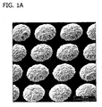
FIGS. 1A ,1B and1C are SEM photographs of solder bumps prepared according to the method described in Example 11. -
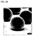
FIGS. 2A ,2B and2C are SEM photographs of reflowed solder bumps prepared according to the method described in Example 12. -
FIG. 3A shows a wafer having a patterned distribution of dies.FIG. 3B shows the measurement position of 5 wager bumps within each die. - In accordance with the present invention, Sn-Ag alloy solder bumps are deposited from an electroplating bath onto an under bump metal structure, such as a silicon wafer substrate overlaid by metallization layers, for use in the manufacture of a microelectronic device. For example, Sn-Ag alloy solder bumps can be deposited having uniform bump heights, uniform Ag content and distribution in the bumps, and good reflow characteristics. Advantageously, the electroplating bath exhibits good stability with respect to Ag immersion/displacement of the Cu under bump metal or soluble Sn anode and plates the Sn-Ag alloy at high current densities. For example, in practice, the plating baths can plate a Sn-Ag alloy at current densities up to 20 amps per square decimeter (Amp/dm2, hereinafter "ASD") with substantially no Ag displacement on Cu UBM or soluble Sn anode. Surprisingly, the plating baths plate Sn-Ag alloy bumps with substantially reduced or eliminated voiding between the bumps and Cu UBM. The invention is described herein in the context of Sn-Ag alloy solder bumps on microelectronic device substrates, which solder bumps are deposited in patterns to yield, for example, the pattern of as-deposited bumps shown in
Figs. 1A ,1B , and1C . These bumps are reflowed to yield the pattern of reflowed bumps shown inFigs. 2A ,2B , and2C . However, the nature of the substrate as an electronic device substrate is not critical to the applicability of the invention. - The present invention stems from the discovery that certain additives to a Sn-Ag electroplating bath increase Ag* ion stability and allow plating at high current densities. The discovered additives substantially reduce the aforementioned problem of spontaneous reduction of Ag* ion onto unintended surfaces, which had detracted from bath stability and uniformity in Sn-Ag proportions in the intended deposits. In one embodiment, to enhance Ag+ ion stability and extend the usable current densities and thereby achieve these advantages, an N-allyl thiourea compound which strongly complexes Ag+ ions is included in the bath. One particular such compound is an N-allyl-N'-hydroxyalkyl thiourea compound. In one embodiment, the alkyl group is ethyl, and the hydroxyl group is in the β position on the ethyl group. This compound, N-allyl-N'-β-hydroxyethyl-thiourea, is hereinafter referred to as "HEAT". The N-allyl thiourea compound which strongly complexes Ag+ ions substantially inhibits Ag+ ion displacement onto the Cu UBM and soluble Sn anode. In one embodiment, Ag+ ion stability is enhanced by including in the bath an amidinothiourea compound which also strongly complexes Ag+ ions. In one preferred embodiment, the amidinothiourea compound is amidinothiourea.
- The formation of the stable silver complex reduces the reduction potential closer to that of Sn2+, such that the current density is not limited by the otherwise rapid Ag+ ion diffusion rate. Instead, the current density is limited by the diffusion rate of Sn2+ ions, which are present typically in such high concentrations, up to about 50 g/L to about 60 g/L or more, that very high current densities can be employed.
- Selected N-allyl thiourea compounds act to increase the solubility of Ag+ ions in the bath by forming complexes with Ag+ ions at acidic pH and to inhibit displacement reactions between Ag+ ions and Cu UBM or soluble Sn anode. Additionally, these N-allyl thiourea compounds shift the Ag+ reduction potential closer to the reduction potential of Sn2+ , allowing for plating at high current densities. Exemplary N-allyl thiourea compounds include N-allyl thiourea, and HEAT. In selecting a suitable N-allyl thiourea compound, compounds which are unable to result in a water soluble complex with Ag+ ions at acidic pH or are toxic are avoided. Based on the HSAB (hard-soft-acid-base) concept and Pi-back bonding of sulfur-containing compounds, it is thought that N-allyl thiourea compounds, such as HEAT, are useful additives for forming complexes with Ag+ ions resulting in tetrahedral complexes with bridged 2e-3 center bonding between Ag-S-Ag. In general, suitable N-allyl thiourea compounds shown below in the following general structure (1):

- Where any of R1, R2, R3, R4, R5, and R6 are heterocycloalkyl or heteroaryl, the ring substituent may comprise O, S, or N atoms. Exemplary substituents on the substituted R groups include halide, hydroxyl, alkoxy, aryl, heteroaryl, nitro, cyano, and mercaptan. In one preferred embodiment, R2, R3, R4, R5, and R6 are H. In another preferred embodiment, R1, R2, R3, R4, R5, and R6 are H, and the compound is N-allyl thiourea. In a particularly preferred embodiment, R2, R3, R4, R5, and R6 are H and R1 is -CH2CH2OH, and the N-allyl thiourea compound is HEAT, which has the following structure (2):

- Selected amidinothiourea compounds act to increase the solubility of Ag+ ions in the bath by forming complexes with Ag+ ions at acidic pH and to inhibit displacement reactions between Ag+ ions and Cu UBM or soluble Sn anode. In selecting a suitable amidinothiourea compound, compounds which are unable to result in a water soluble complex with Ag+ ions at acidic pH or are toxic are avoided.' The general formula of suitable amidinothiourea compounds are shown below in the following formula (3):

- R8 and R9 are either S or N, and when R8 is S, R9 is N and when R8 is N, R9 is S; and
- R10, R11, R12, and R13 are each independently H, OH, hydrocarbyl, substituted hydrocarbyl, heterocycloalkyl, substituted heterocycloalkyl, alkoxy, substituted alkoxy, aryl, substituted aryl, heteroaryl, or substituted heteroaryl.
- Exemplary substituents on the substituted R10, R11, R12, and R13 include halide, hydroxyl, alkyl, alkoxy, aryl, heteroaryl, nitro, cyano, and mercaptan. In one preferred embodiment, R10, R11, R12, and R13 are all hydrogen, and the amidinothiourea compound is amidinothiourea, which has the following structure (4):

- In the baths of the present invention, the concentration of the N-allyl-thiourea compound or amidinothiourea compound is between about 0.5 g/L and about 24 g/L. Employing too much of the compound causes decomposition to free thiourea derivative. Employing too little results in insufficient complexing of Ag. In one embodiment, the concentration is at least about 1 g/L, such as about 1.4 g/L, about 1.5 g/L, about 1.75 g/L, or about 2.2 g/L. In one embodiment, the concentration is no greater than about 8 g/L, such as about 8 g/L, about 6 g/L, about 4 g/L, or about 3 g/L. In one embodiment, between about 0.5 g/L and about 16 g/L of HEAT is added to complex Ag+ ions and enhance their solubility, while also inhibiting displacement reactions between Ag+ ions and Cu UBM or soluble Sn anode. In one embodiment, between about 0.5 g/L and about 16 g/L, such as between about 1 and about 8 g/L of amidinothiourea is added to complex Ag+ ions and enhance their solubility.
- Silver immersion plating (also known as "displacement" plating) occurs in electroplating baths spontaneously due to high nobility of Ag+ ions. The reduction of Ag is described by the following reaction:
1) Ag+ + e- ---> Ag E° = +0.80 V v. S.H.E.
The positive value of E° for the reaction indicates the very positive redox potential of Ag+. Cu2+ and Sn4+ are less noble than Ag+ as shown by the lower reduction potentials of the following reduction reactions:
2) Cu2+ + 2e- ---> Cu E° = +0.34 V v. S.H.E.
3) Sn4+ + 2e- ---> Sn2+ E° = +0.15 V v. S.H.E.
Accordingly, upon exposure of aqueous Ag+ ions to aqueous Sn2+ ions and/or Cu UBM, Ag+ ions spontaneously oxidize Sn2+ ions to Sn4+ ions and Cu metal to Cu2+ ions. Concurrently, Ag+ ions are reduced to Ag metal, which may become a finely divided metal floating in solution or deposit spontaneously on the substrate, walls of the plating tank, or soluble Sn anode. Spontaneous Ag+ ion displacement plating renders difficult control of the concentration of Ag+ ions in the electroplating bath, which is a severe limitation in the use of Ag in electroplating alloys, such as in Sn-based solder wafer bumps. Accordingly, the thiourea compounds, such as HEAT and amidinothiourea, are added to the Sn-Ag electroplating bath to complex Ag+ ions and thereby control both the solubility and stability of Ag+ ions in the plating bath. Advantageously, HEAT and amidinothiourea also lower the reduction potential of Ag+ ions, bringing that potential closer to the reduction potential of Sn2+ ions, which allows for better control of the concentration and uniformity of Ag metal in the Sn-Ag alloy solder wafer bump and allows for plating at high current densities. - To further enhance the effect of thiourea compounds for extending the usable current density range, certain quaternary ammonium surfactants are added to the bath in the currently preferred embodiment. The quaternary ammonium surfactants which have been found useful for adding to the plating baths of the present invention include alkyl dimethyl benzyl ammonium salts in which the alkyl group is between 10 and 18 carbons long, preferably the alkyl group is 12 to 14 carbons long. The alkyl group may be substituted or unsubstituted. A particularly preferred quaternary ammonium surfactant is a C12/C14 dimethyl benzyl ammonium chloride salt sold under the trade name Dodigen 226, which comprises lauryl dimethyl benzyl ammonium chloride salt and myristyl dimethyl benzyl ammonium chloride salt. Advantageously, this compound acts additionally as a grain refiner and prevents nodular growth. The quaternary ammonium surfactants further extend the useful current density range, act as grain refiners, and inhibit nodular growth. Without being bound to a particular theory, it is thought that the quaternary ammonium surfactants further extend the current density range because the salts can bind both Sn2+ and Ag+ ions, thus inhibiting diffusion of those metal ions and allowing the plating current density range to be extended.
- In the baths of the present invention, the concentration of quaternary ammonium surfactant is between about 0.1 g/L and about 20 g/L, preferably between about 0.8 and about 15 g/L, such as about 0.8 g/L, about 1.6 g/L, or about 2.0 g/L. For example, between about 0.5 g/L and about 10 g/L of Dodigen 226 may be added to extend the useful current density range, refine the grain size, and prevent nodular growth in the Sn-Ag solder wafer bump. Employing too much of the compound causes bath instability and increased nodule formation at the center of wafers. Employing too little results in insufficient suppression of high current density plating, and therefore increases the risk of nodule growth at high current density areas.
- In conventional Sn-Ag electroplating baths, the plating rate is limited to low current densities. Typically, the current densities practically achievable in conventional plating baths are no greater than about 1 ASD. Limited current densities adversely affect plating throughput. Conventional baths are limited to such low current densities because of rapid diffusion rate of Ag+ ions in the bath. The electroplating baths of the current invention comprising thiourea compounds, such as HEAT and amidinothiourea, and quaternary ammonium surfactant salts, such as Dodigen 226, can be plated at current densities up to about 20 ASD. By incorporating these additives, the increased solubility and stability of Ag+ ions in the bath largely remove Ag+ ion diffusion rate as an overall rate limiting aspect, and makes it so Sn2+ diffusion rate is the overall rate limiting aspect. Since the Sn2+ ion concentration is in the range of about 50 g/L to about 60 g/L, the diffusion rate limited current is much higher. Taking advantage of this discovery, the process of the invention employs a current density of greater than about 4 ASD. One preferred embodiment employs a current density of greater than 8 ASD, and another preferred high-throughput embodiment employs a current density of more than 10 ASD.
- Among other components of the bath may be added a source of Sn2+ ions, a source of Ag+ ions, an anti-oxidant, and a surfactant.
- The source of Sn2+ ions may be a soluble anode comprising a Sn2+ salt, or, where an insoluble anode is used, a soluble Sn2+ salt. In both cases, the Sn2+ salt is Sn(CH3SO3)2 (Tin methane sulfonic acid, hereinafter "Sn(MSA)2") in one preferred embodiment. Sn(MSA)2 is a preferred source of Sn2+ ions because of its high solubility. Additionally, the pH of Sn-Ag plating baths of the present invention may be lowered using methane sulfonic acid, and the use of Sn(MSA)2 as the Sn source rather than, e.g., Sn(X), avoids the introduction of unnecessary additional anions, e.g., X2-, into the plating baths, especially those that render Ag+ substantially insoluble. Typically, the concentration of the source of Sn2+ ions-is sufficient to provide between about 10 g/L and about 100 g/L of Sn2+ ions into the bath, preferably between about 15 g/L and about 95 g/L, more preferably between about 40 g/L and about 60 g/L. For example, Sn(MSA)2 may be added to provide between about 30 g/L and about 60 g/L Sn2+ ions to the plating bath.
- Ag+ ions are sparingly soluble with most anions. Therefore, the source of Ag+ ions is limited to salts of nitrate, acetate, and preferably methane sulfonate. Typically, the concentration of the source of Ag+ ions is sufficient to provide between about 0.1 g/L and about 1.5 g/L of Ag+ ions into the bath, preferably between about 0.3 g/L and about 0.7 g/L, more preferably between about 0.4 g/L and about 0.6 g/L. For example, Ag (MSA) may be added to provide between about 0.2 g/L and about 1.0 g/L Ag+ ions to the plating bath.
- Anti-oxidants may be added to the baths of the present invention to stabilize the bath against oxidation of Sn2+ ions in solution. In the electroplating baths for plating Sn-Ag alloy solder wafer bumps, Ag+ ions, being nobler than Sn2+, can spontaneously oxidize Sn2+ to Sn4+, as explained above. This spontaneous redox reaction can cause Ag metal to deposit on the Cu UBM, the walls of the plating tank, or the soluble Sn anode, and to form finely divided Ag metal particles in solution. Additionally, reduction of Sn4+, which forms stable hydroxides and oxides, to Sn metal, being a 4-electron process, slows the reaction kinetics. Although HEAT and other thiourea compounds may be added to the bath to prevent the spontaneous reduction of Ag+/oxidation of Sn2+, it is preferable to add an anti-oxidant to the bath to further stabilize the bath against this redox reaction. Accordingly, preferred anti-oxidants such as hydroquinone, catechol, and any of the hydroxyl, dihydroxyl, or trihydroxyl benzoic acids may be added in a concentration between about and about, preferably between about 0.1 g/L and about 10 g/L, more preferably between about 0.5 g/L and about 3 g/L. For example, hydroquinone may be added to the bath at a concentration of about 2 g/L.
- Surfactants may be added to promote wetting of the under bump metal structure and resist material and enhance the deposition of the wafer bumps. The surfactant seems to serve as a mild deposition inhibitor which can suppress three-dimensional growth to an extent, thereby improving morphology and topography of the film. It can also help refine the grain size, which yields a more uniform bump. Exemplary anionic surfactants include alkyl phosphonates, alkyl ether phosphates, alkyl sulfates, alkyl ether sulfates, alkyl sulfonates, alkyl ether sulfonates, carboxylic acid ethers, carboxylic acid esters, alkyl aryl sulfonates, aryl alkylether sulfonates, aryl sulfonates, and sulfosuccinates. A particularly preferred anionic surfactant is Ralufon NAPE 14-90 (available from Raschig GmbH, Ludwigshafen, Germany) which is a sulfonated β-naphthol propoxylate/ethoxylate having a block of propylene oxide units bonded to the β-naphthol hydroxyl group, a block of ethylene oxide units bonded to the propylene oxide block, and a terminal propane sulfonate group. Exemplary cationic surfactants include quaternary ammonium salts such as dodecyl trimethyl ammonium chloride, cetyl trimethyl ammonium chloride, and the like. Exemplary non-ionic surfactants include glycol and glycerol esters, polyethylene glycols, and polypropylene glycol/polyethylene glycol. Preferred non-ionic surfactants include β-naphthol derivatives, such as β-naphtholethoxylates having between 1 and about 24 ethylene oxide monomer units bonded to the β-naphthol hydroxyl group, more preferably between about 8 and about 16 ethylene oxide monomer units. A particularly preferred non-ionic surfactant is Lugalvan BNO12 which is a β-naphtholethoxylate having 12 ethylene oxide monomer units bonded to the naphthol hydroxyl group. The surfactant can be present in the electroplating bath at a concentration between about 0.1 g/L and about 50 g/L, preferably between about 5 g/L and about 20 g/L.
- The electrolytic plating bath of the present invention preferably has an acidic pH to inhibit anodic passivation, achieve better cathodic efficiency, and achieve a more ductile deposit. Accordingly, the bath pH is preferably between about 0 and about 3. In the preferred embodiment the pH of the bath is 0. The choice of acids is limited by the poor solubility or substantial insolubility of most Ag salts. Accordingly, the preferred acidic pH can be achieved using nitric acid, acetic acid, and methane sulfonic acid. In one preferred embodiment, the acid is methane sulfonic acid. The concentration of the acid is preferably between about 50 g/L and about 200 g/L, more preferably between about 70 g/L and about 120 g/L. For example, between about 50 g/L and about 160 g/L methane sulfonic acid can be added to the electroplating bath to achieve a bath of pH 0 and act as the conductive electrolyte.
- The electroplating baths of the present invention are preferably employed to plate Sn-Ag alloy solder wafer bumps on Cu UBM in the manufacture of microelectronic devices, such as printed wiring boards (PWB). However, the plating baths may be used in any application requiring a Sn-based solder wafer bump. Advantageously, the plating baths may plate at.high rates due to the stability of the bath and the high current densities which may be applied.
- In one application for the invention, the goal of the process is to yield the product of
FIGS. 1 and2 , which is an electronic device substrate with individual solder bumps thereon. With regard to the specific process, a first step is substrate preparation. The substrate preparation is not narrowly germane to the present invention; but to place the invention in context, it is noted that the invention falls within the following overall context proceeding from substrate preparation through inspection: - 1) receiving photoresist patterned wafer with a sputtered Cu seed layer or Cu UBM (thickness of this layer is normally between 300Å and 3000Å)
- 2) deposit a second UBM layer to prevent diffusion of Cu into solder bumps such as SnAg (thickness of this layer is normally 1 to 3 microns)
- 3) deposit solder bumps such as SnAg, normally into mushroom shape (bump height varies from about 50 microns to 100 microns)
- 4) strip off photoresist
- 5) etch off Cu UBM
- 6) reflow SnAg bumps
- 7) inspect and characterization such as bump height and Ag alloy uniformity measurements, voiding analysis, etc.
- During the electrolytic plating operation of the invention for bumping, the plating solution is preferably maintained at a temperature between about 15°C and about 50°C. In one preferred embodiment, the temperature is between about 25°C and about 35°C. The substrate is immersed in or otherwise exposed to the plating bath. The current density applied is between about 1 A/dm2 and about 20 A/dm2, preferably between about 1 A/dm2 and about 16 A/dm2 as described above. At these current densities, the plating rate is between about 1 µm/min and about 10 µm/min. Typically, the thickness of the electrolytically deposited Sn-Ag alloy solder wafer bump is between about 10 µm and about 100 µm which, in view of the foregoing plating rates, corresponds to the substrate being immersed in the solution for a duration between about 10 minutes and about 30 minutes.
- The anode may be a soluble anode or insoluble anode. If a soluble anode is used, the anode preferably comprises Sn (MSA)2, such that the source of Sn2+ ions in the plating bath is the soluble anode. Use of a soluble anode is advantageous because it allows careful control of the Sn2+ ion concentration in the bath, such that the Sn2+ ion does not become either under- or over- concentrated. An insoluble anode may be used instead of a Sn-based soluble anode. Preferable insoluble anodes include Pt/Ti, Pt/Nb, and DSAs (dimensionally stable anodes). If an insoluble anode is used, the Sn2+ ions are introduced as a soluble Sn2+ salt.
- During the plating operation, Sn2+ ions and Ag+ ions are depleted from the electrolytic plating solution. Rapid depletion can occur especially with the high current densities achievable with the plating baths of the present invention. Therefore, Sn2+ ions and Ag+ ions may be replenished according to a variety of methods. If a Sn-based soluble anode is used, the Sn2+ ions are replenished by the dissolution of the anode during the plating operation. If an insoluble anode is used, the electrolytic plating solution may be replenished according to continuous mode plating methods or use-and-dispose plating methods. In the continuous mode, the same bath volume is used to treat a large number of substrates. In this mode, reactants must be periodically replenished, and reaction products accumulate, necessitating periodic filtering of the plating bath. Alternatively, the electrolytic plating compositions according to the present invention are suited for so-called "use-and-dispose" deposition processes. In the use-and-dispose mode, the plating composition is used to treat a substrate, and then the bath volume is directed to a waste stream. Although this latter method may be more expensive, the use-and-dispose mode requires no metrology; that is, measuring and adjusting the solution composition to maintain bath stability is not required.
- After electroplating of the SnAg solder bumps is complete, flux is generously applied with a spray to coat the entire wafer. Preferably, sufficient flux is applied to impregnate every bump with flux. After application of flux, the bumps may be reflowed according to methods known in the art.
- Electroplating baths of the present invention are advantageously stable to spontaneous Ag+ ion reduction and can be plated at current densities which are higher than those achievable by conventional plating baths. The electroplating baths can be used to plate Sn-Ag alloys having Ag metal content between about 1 wt. % and about 4 wt. %, preferably between about 2 wt. % and about 3 wt. %, the process therefore offering the capability to plate Sn-Ag alloys having a wide range of melting points between about 221°C and about 226°C. The Sn-Ag solder wafer bumps are plated with substantially reduced or eliminated voiding between the bump and the Cu UBM. Moreover, because of the Ag+ ion stabilizing components of the baths.of the present invention, the Ag metal is distributed uniformly in the Sn-Ag alloys. This uniformity is important for successful reflow. It also ensures that the bump properties and mechanical strength are uniform across the wafer or other substrate.
- The following examples further illustrate the present invention.
- A Sn-Ag bath for electroplating Sn-Ag alloy solder wafer bumps was prepared comprising the following components:
- 2.22 g/L HEAT
- 60 g/L Sn2+ as 156 g/L Sn (MSA)2
- 0,5 g/L Ag+ as 0.94 g/L Ag(MSA)
- 100 mL/L MSA (70% solution)
- 2 g/L Hydroquinone
- 7.0 g/L of Lugalvan BNO12
- 1.6 g/L of Dodigen 226
- pH 0
- Optionally, the bath may comprise 0.5 grams per liter of Defoamer SF.
- One liter of this bath was prepared according to the following protocol:
- 1) Water (about 400 mL) added to a 1 L flask.
- 2) MSA (100 mL of 70% solution) added and solution stirred.
- 3) HEAT (2.22 g) added and solution stirred for about 5 minutes.
- 4) Ag (MSA) (0.84 g) added and solution stirred for about 5 minutes.
- 5) Hydroquinone (2 g) added and solution stirred for about 5 minutes.
- 6) Sn(MSA)2 (156 g) added and solution stirred for about 5 minutes.
- 7) Lugalvan BNO12 (7.0 g) added and solution stirred for about 5 minutes.
- 8) With vigorous mixing, Dodigen 226 (1.6 g in aqueous solution) added dropwise.
- 9) Add water to 1 L.
- This mixing order has been discovered to advantageously result in increased stability. In particular, mixing the complexing agent and the Ag source together and providing a period of mixing prior to adding the Sn source, and prior to adding the surfactant, has been found to increase stability. It preliminarily appears to provide advantages in complexing to allow early intimate contact between the complexor and the Ag+ ions prior to the introduction of certain other ingredients. Accordingly, this preferred process involves combining the source of Ag+ ions with the complexor for Ag+ ions and water to form a bath precursor comprising Ag+ ion complex in a substantial absence of the source of Sn+2 ions. By "substantial absence" it is meant that 90% or more of the overall source of Sn+2 ions is not added until after intimate mixing of the complexor and the source of Ag+ ions. It is also seen that in this preferred embodiment, the bath precursor is substantially free of surfactant, and the process involves adding the surfactant to the bath precursor after formation of the Ag complex.
- Another Sn-Ag plating bath was prepared comprising the following components:
- 1.75 g/L HEAT
- 60 g/L Sn2+ as 156 g/L Sn(MSA)2
- 0.5 g/L Ag+ as 0.94 g/L Ag (MSA)
- 100 mL/L MSA (70% solution)
- 2 g/L Hydroquinone
- 7.0 g/L of Lugalvan BNO12
- 1.6 g/L of Dodigen 226.
- Another bath was prepared comprising the following components:
- 2.22 g/L HEAT
- 60 g/L Sn2+ as 156 g/L Sn (MSA)2
- 0.5 g/L Ag+ as 0.94 g/L Ag (MSA)
- 100 mL/L MSA (70% solution)
- 2 g/L Hydroquinone
- 7.0 g/L of Lugalvan BNO12
- 1.6 g/L of Dodigen 226
- 0.5 g/L of Defoamer SF.
- Another bath was prepared comprising the following components:
- 1.4 g/L HEAT
- 60 g/L Sn2+ as 156 g/L Sn (MSA)2
- 0.5 g/L Ag+ as 0.94 g/L Ag (MSA)
- 140 mL/L MSA (70% solution)
- 2 g/L Hydroquinone
- 6.7 g/L of Lugalvan BNO12
- 0.8 g/L of Dodigen 226.
- Another bath was prepared comprising the following components:
- 8 g/L HEAT
- 60 g/L Sn2+ as 156 g/L Sn (MSA)2
- 0.5 g/L Ag+ as 0.94 g/L Ag (MSA)
- 160 mL/L MSA (70% solution)
- 2 g/L Hydroquinone
- 8 g/L Ralufon NAPE 1490.
- Another bath was prepared comprising the following components:
- 6 g/L HEAT
- 40 g/L Sn2+ as 104 g/L Sn (MSA)2
- 0.4 g/L Ag+ as 0.75 g/L Ag (MSA)
- 300 mL/L MSA (70% solution)
- 2 g/L Hydroquinone
- 8 g/L Ralufon NAPE 1490.
- Another bath was prepared comprising the following components:
- 3 g/L N,N'-Diethylthiourea (DETU)
- 60 g/L Sn2+ as 156 g/L Sn (MSA)2
- 0.5 g/L Ag+ as 0.94 g/L Ag (MSA)
- 180 mL/L MSA (70% solution)
- 2 g/L Hydroquinone
- 7 g/L Lugalvan BNO 12
- 2 g/L Dodigen 226.
- Another bath was prepared comprising the following components:
- 1.5 g Amidinothiourea
- 60 g/L Sn2+ as 156 g/L Sn (MSA)2
- 1 g/L Ag+ as 1.88 g/L Ag(MSA)
- 180 mL/L MSA (70% solution)
- 2 g/L Hydroquinone.
- Another bath was prepared comprising the following components:
- 3 g/L N,N'-Dimethylthiourea
- 30 g/L Sn2+ as 78 g/L Sn(MSA)2
- 0.3 g/L Ag+ as 0.56 g/L Ag(MSA)
- 150 mL/L MSA (70% solution)
- 2 g/L Hydroquinone
- 8 g/L Ralufon NAPE 1490.
- Another bath was prepared comprising the following components:
- 4 g/L N-Allyl-thiourea
- 60 g/L Sn2+ as 156 g/L Sn (MSA)2
- 0.5 g/L Ag+ as 0.94 g/L Ag(MSA)
- 100 mL/L MSA (70% solution)
- 2 g/L Hydroquinone
- 7 g/L Lugalvan BNO 12
- 2 g/L Dodigen 226.
- Sn-Ag wafer bumps were plated on Cu UBM using the bath of Example 1. The silicon wafer and Cu UBM die pattern was prepared as described above. Uncrosslinked photo resistant material was stripped from the wafer using methylene chloride and ultrasonic agitation for between 30 and 60 minutes. Cu metallization was etched by a solution comprising deionized water (60 mL), ammonium hydroxide (60 mL, 20 to 24% solution), and hydrogen peroxide (10 mL, 3% solution).
- Sn-Ag solder wafer bumps were plated from the bath of Example 1 onto dies on patterned silicon wafer. The die positions on the wafer and bump positions within each die are shown in
FIGs. 3A and 3B . The bumps were plated at 12 ASD. Bump height distribution was measured by surface profilometry (DEKTAK 8000). Table I shows bump height distribution data obtained from the profilometer. Bump composition was measured by SEM/EDS (20 kV). Table II shows the Ag content (in wt. %) data obtained by SEM/EDS. Wafer bump topography was measured using SEM (20 kV, 45° tilt).FIGs. 1A ,1B ,1C are SEM photographs showing the Sn-Ag solder wafer bumps as deposited at 200x, 800x, and 3000x magnification, respectively. For each measurement technique, 5 bumps (bump pattern shown inFIG. 3B and designated 1, 2, 3, 4, and 5 in the horizontal axes in Tables I and II below) were analyzed at each of 3 die positions (die pattern shown inFIG. 3A and designated 3, 6, 7 in the vertical axes in Tables I and II below).Table I. Sn-Ag Solder Bump Height Measurements Plating Conditions: 12 ASD, 0.8 Hours Die No. Measured Bumps ( µm) 1 2 3 4 5 Die Average 3 64.0 62.0 64.0 62.0 58.0 62.0 6 64.0 63.0 64.0 65.0 58.0 62.8 7 64.0 62.0 64.0 64.0 59.0 62.6 Maximum Height (µm) Minimum Height (µm) Range (µm) Average Height (µm) Standard Deviation (µm) Range/ Average (%) Deviation/ Average (%) 65.0 58.0 7.0 62.5 2.3 11.2 3.7 Table II. Sn-Ag Solder Bump Ag Content Measurements Plating Conditions: 12 ASD, 0.8 Hours Die No. Measured Bumps (Ag wt. %) 1 2 3 4 5 Die Average 3 2.35 2.26 2.99 3.15 2.52 2.65 6 1.80 2.39 1.78 1.54 2.15 1.93 7 2.85 2.80 2.25 2.25 2.33 2.50 Maximum (Ag wt. %) Minimum (Ag wt. %) Range (Ag wt. %) Average (Ag wt. %) Standard Deviation (Ag wt. %) Range/ Average (%) Deviation/ Average (%) 3.15 1.54 1.61 2.36 0.45 68.20 19.22 - The Sn-Ag solder wafer bumps of Example 3 were reflowed using a hot plate in a glove box. Steps:
- 1. Flux application: Lonco 3355-11
- 2. Preheat: to evaporate volatiles, allow flux to activate, and bond to surface
- 3. Reflow: temperature of hot plate is 260°C and nitrogen atmosphere.
- 4. Cooling: air cooling
- Reflowed wafer bumps were photographed using SEM (20 kV, 75° tilt).
FIGs. 2A ,2B ,2C are SEM photographs showing reflowed Sn-Ag solder wafer bumps as deposited at 200x, 800x, and 3000x magnification, respectively. The reflowed bumps are smooth and show a uniform ball shape, and demonstrate zero voiding. - In view of the above, it will be seen that the several objects of the invention are achieved and other advantageous results attained.
- When introducing elements of the present invention or the preferred embodiment(s) thereof, the articles "a", "an", "the" and "said" are intended to mean that there are one or more of the elements. For example, that the foregoing description and following claims refer to "a" wafer bump means that there are one or more such bumps. The terms "comprising", "including" and "having" are intended to be inclusive and mean that there may be additional elements other than the listed elements.
- As various changes could be made in the above without departing from the scope of the invention, it is intended that all matter contained in the above description and shown in the accompanying drawings shall be interpreted as illustrative and not in a limiting sense.
Claims (12)
- An electroplating composition for plating a Sn-Ag solder bump comprising:a source of Sn2+ ions;a source of Ag+ ions; anda N-allyl-thiourea compound, wherein the N-allyl-thiourea compound has a formula (I):

- The electroplating composition of claim 1 wherein R2, R3, R4, R5, and R6 are H.
- The electroplating composition of claim 1 or 2 further comprising a quaternary ammonium surfactant.
- The electroplating composition of claim 3 wherein the quaternary ammonium surfactant comprises an alkyl dimethyl benzyl ammonium surfactant.
- The electroplating composition of claim 3 wherein the quaternary ammonium surfactant comprises lauryl benzyl dimethyl ammonium chloride and myristyl benzyl dimethyl ammonium chloride.
- The electroplating composition of any one of claims 1 through 5 wherein the electroplating composition further comprises a β-naphthol derivative.
- The electroplating composition of claim 6 wherein the β-naphthol derivative comprises a sulfonated β-naphthol propoxylate/ethoxylate.
- The electroplating composition of any one of claims 1 through 5 wherein the electroplating composition further comprises hydroquinone.
- An electroplating composition for plating a Sn-Ag solder bump comprising:a source of Sn2+ ions;a source of Ag+ ions; andan amidinothiourea compound.
- The electroplating composition of claim 9 wherein the amidinothiourea compound has the formula (II):
 R8 and R9 are either S or N, and when R8 is S, R9 is N and when R8 is N, R9 is S; andR10, R11, R12, and R13 are each independently H, OH, hydrocarbyl, substituted hydrocarbyl, heterocycloalkyl, substituted heterocycloalkyl, alkoxy, substituted alkoxy, aryl, substituted aryl, heteroaryl, or substituted heteroaryl.
 - The electroplating composition of claim 9 wherein the amidinothiourea compound has the formula (III):

- A process for forming a solder bump on an under bump metal structure in the manufacture of a microelectronic device, the process comprising:exposing the under bump metal structure to the electroplating composition of any one of claims 1 through 11; andsupplying an external source of electrons to the electrolytic bath to deposit a Sn-Ag alloy onto the under bump metal structure.
Applications Claiming Priority (3)
| Application Number | Priority Date | Filing Date | Title |
|---|---|---|---|
| US70832805P | 2005-08-15 | 2005-08-15 | |
| US11/463,355 US7713859B2 (en) | 2005-08-15 | 2006-08-09 | Tin-silver solder bumping in electronics manufacture |
| PCT/US2006/031618 WO2007022075A2 (en) | 2005-08-15 | 2006-08-14 | Tin-silver solder bumping in electronics manufacture |
Publications (3)
| Publication Number | Publication Date |
|---|---|
| EP1946362A2 EP1946362A2 (en) | 2008-07-23 |
| EP1946362A4 EP1946362A4 (en) | 2010-01-06 |
| EP1946362B1 true EP1946362B1 (en) | 2012-01-11 |
Family
ID=37743065
Family Applications (1)
| Application Number | Title | Priority Date | Filing Date |
|---|---|---|---|
| EP06801412A Active EP1946362B1 (en) | 2005-08-15 | 2006-08-14 | Tin-silver solder bumping in electronics manufacture |
Country Status (7)
| Country | Link |
|---|---|
| US (1) | US7713859B2 (en) |
| EP (1) | EP1946362B1 (en) |
| JP (1) | JP5207968B2 (en) |
| KR (1) | KR101361305B1 (en) |
| CN (1) | CN101622701B (en) |
| AT (1) | ATE541306T1 (en) |
| WO (1) | WO2007022075A2 (en) |
Families Citing this family (31)
| Publication number | Priority date | Publication date | Assignee | Title |
|---|---|---|---|---|
| US7291201B2 (en) * | 2004-08-30 | 2007-11-06 | National Tsing Hua University | Method for making nano-scale lead-free solder |
| TW200735198A (en) * | 2006-03-01 | 2007-09-16 | Advanced Semiconductor Eng | The method for removing the residual flux |
| US20090145764A1 (en) * | 2007-12-11 | 2009-06-11 | Enthone Inc. | Composite coatings for whisker reduction |
| US8226807B2 (en) * | 2007-12-11 | 2012-07-24 | Enthone Inc. | Composite coatings for whisker reduction |
| JP2009191335A (en) * | 2008-02-15 | 2009-08-27 | Ishihara Chem Co Ltd | Plating solution and electronic parts |
| JP4724192B2 (en) * | 2008-02-28 | 2011-07-13 | 株式会社東芝 | Manufacturing method of electronic parts |
| EP2221396A1 (en) * | 2008-12-31 | 2010-08-25 | Rohm and Haas Electronic Materials LLC | Lead-Free Tin Alloy Electroplating Compositions and Methods |
| US9175400B2 (en) * | 2009-10-28 | 2015-11-03 | Enthone Inc. | Immersion tin silver plating in electronics manufacture |
| US9005409B2 (en) | 2011-04-14 | 2015-04-14 | Tel Nexx, Inc. | Electro chemical deposition and replenishment apparatus |
| US9017528B2 (en) | 2011-04-14 | 2015-04-28 | Tel Nexx, Inc. | Electro chemical deposition and replenishment apparatus |
| US8113412B1 (en) * | 2011-05-13 | 2012-02-14 | Taiwan Semiconductor Manufacturing Company, Ltd | Methods for detecting defect connections between metal bumps |
| CN103540971A (en) * | 2013-10-29 | 2014-01-29 | 常熟市伟达电镀有限责任公司 | Highly-conductive electroplating liquid |
| US9303329B2 (en) | 2013-11-11 | 2016-04-05 | Tel Nexx, Inc. | Electrochemical deposition apparatus with remote catholyte fluid management |
| US8877630B1 (en) * | 2013-11-12 | 2014-11-04 | Chipmos Technologies Inc. | Semiconductor structure having a silver alloy bump body and manufacturing method thereof |
| US9368340B2 (en) * | 2014-06-02 | 2016-06-14 | Lam Research Corporation | Metallization of the wafer edge for optimized electroplating performance on resistive substrates |
| US9604316B2 (en) | 2014-09-23 | 2017-03-28 | Globalfoundries Inc. | Tin-based solder composition with low void characteristic |
| TWI559829B (en) * | 2014-10-22 | 2016-11-21 | 矽品精密工業股份有限公司 | Package structure and method of fabricating the same |
| WO2016152986A1 (en) * | 2015-03-26 | 2016-09-29 | 三菱マテリアル株式会社 | Plating solution using ammonium salt |
| JP6631349B2 (en) * | 2015-03-26 | 2020-01-15 | 三菱マテリアル株式会社 | Plating solution using ammonium salt |
| KR101722703B1 (en) | 2015-04-10 | 2017-04-03 | 엘티씨에이엠 주식회사 | Tin-silver solder bump plating solution |
| US20160308100A1 (en) * | 2015-04-17 | 2016-10-20 | Chipmos Technologies Inc | Semiconductor package and method of manufacturing thereof |
| US10793956B2 (en) * | 2015-08-29 | 2020-10-06 | Mitsubishi Materials Corporation | Additive for high-purity copper electrolytic refining and method of producing high-purity copper |
| JP6733313B2 (en) * | 2015-08-29 | 2020-07-29 | 三菱マテリアル株式会社 | High-purity copper electrolytic refining additive and high-purity copper manufacturing method |
| KR101722704B1 (en) * | 2015-12-16 | 2017-04-11 | 엘티씨에이엠 주식회사 | Tin-silver solder bump high speed plating solution and the manufacturing method thereof |
| CN106757212B (en) * | 2016-11-30 | 2018-02-02 | 昆山成功环保科技有限公司 | ELECTROPLATING Sn-Ag ALLOY solution for wafer-level packaging |
| KR102634249B1 (en) | 2018-12-27 | 2024-02-07 | 솔브레인 주식회사 | Plating Composition and Method for Forming The Solder Bump |
| CN111690958B (en) * | 2019-03-15 | 2023-07-28 | 上海新阳半导体材料股份有限公司 | Tin plating solution, preparation method and application thereof |
| US11280014B2 (en) | 2020-06-05 | 2022-03-22 | Macdermid Enthone Inc. | Silver/tin electroplating bath and method of using the same |
| CN112359380A (en) * | 2020-10-23 | 2021-02-12 | 珠海鑫通化工有限公司 | Electroplating solution for chemical tinning of passive component |
| CN115029745A (en) * | 2022-07-08 | 2022-09-09 | 云南锡业集团(控股)有限责任公司研发中心 | Method capable of reducing element plating process steps and improving welding spot reliability |
| CN115070259A (en) * | 2022-07-15 | 2022-09-20 | 深圳市同方电子新材料有限公司 | Novel environment-friendly lead-free soldering paste of superfine soldering tin powder |
Family Cites Families (28)
| Publication number | Priority date | Publication date | Assignee | Title |
|---|---|---|---|---|
| US4293391A (en) | 1980-04-02 | 1981-10-06 | Rohco, Inc. | Cadmium plating baths and methods for electrodepositing bright cadmium deposits |
| JPS5967387A (en) * | 1982-10-08 | 1984-04-17 | Hiyougoken | Tin, lead and tin-lead alloy plating bath |
| EP0126220A1 (en) * | 1983-04-26 | 1984-11-28 | Hüls Aktiengesellschaft | Pickling solution for metallic surfaces, and its use |
| US4582576A (en) | 1985-03-26 | 1986-04-15 | Mcgean-Rohco, Inc. | Plating bath and method for electroplating tin and/or lead |
| US4749626A (en) | 1985-08-05 | 1988-06-07 | Olin Corporation | Whisker resistant tin coatings and baths and methods for making such coatings |
| US4715894A (en) | 1985-08-29 | 1987-12-29 | Techno Instruments Investments 1983 Ltd. | Use of immersion tin and tin alloys as a bonding medium for multilayer circuits |
| JPS642330A (en) | 1987-06-25 | 1989-01-06 | Nippon Mining Co Ltd | Film carrier and manufacture thereof |
| JP3538499B2 (en) * | 1996-05-15 | 2004-06-14 | 株式会社大和化成研究所 | Tin-silver alloy electroplating bath |
| US6099713A (en) | 1996-11-25 | 2000-08-08 | C. Uyemura & Co., Ltd. | Tin-silver alloy electroplating bath and tin-silver alloy electroplating process |
| JP3776566B2 (en) * | 1997-07-01 | 2006-05-17 | 株式会社大和化成研究所 | Plating method |
| JP3782869B2 (en) * | 1997-07-01 | 2006-06-07 | 株式会社大和化成研究所 | Tin-silver alloy plating bath |
| JP3904333B2 (en) * | 1998-09-02 | 2007-04-11 | 株式会社大和化成研究所 | Tin or tin alloy plating bath |
| JP2000265294A (en) * | 1999-03-15 | 2000-09-26 | Matsushita Electric Ind Co Ltd | Tin and tin alloy plating bath, plating film and lead frame for semiconductor device |
| JP3433291B2 (en) | 1999-09-27 | 2003-08-04 | 石原薬品株式会社 | Tin-copper-containing alloy plating bath, tin-copper-containing alloy plating method, and article formed with tin-copper-containing alloy plating film |
| US6361823B1 (en) | 1999-12-03 | 2002-03-26 | Atotech Deutschland Gmbh | Process for whisker-free aqueous electroless tin plating |
| US6638847B1 (en) | 2000-04-19 | 2003-10-28 | Advanced Interconnect Technology Ltd. | Method of forming lead-free bump interconnections |
| DE10026680C1 (en) | 2000-05-30 | 2002-02-21 | Schloetter Fa Dr Ing Max | Electrolyte and method for depositing tin-silver alloy layers and use of the electrolyte |
| US6706418B2 (en) | 2000-07-01 | 2004-03-16 | Shipley Company L.L.C. | Metal alloy compositions and plating methods related thereto |
| CN1280452C (en) * | 2001-05-09 | 2006-10-18 | 荏原优莱特科技股份有限公司 | Copper plating bath and method for plating substrate by using the same |
| US20030000846A1 (en) | 2001-05-25 | 2003-01-02 | Shipley Company, L.L.C. | Plating method |
| WO2003014426A1 (en) | 2001-07-31 | 2003-02-20 | Sekisui Chemical Co., Ltd. | Method for producing electroconductive particles |
| JP3881614B2 (en) | 2002-05-20 | 2007-02-14 | 株式会社大和化成研究所 | Circuit pattern forming method |
| US7273540B2 (en) | 2002-07-25 | 2007-09-25 | Shinryo Electronics Co., Ltd. | Tin-silver-copper plating solution, plating film containing the same, and method for forming the plating film |
| US20040025384A1 (en) | 2002-08-09 | 2004-02-12 | Ptacek Robert J. | Point of purchase display |
| US7012333B2 (en) * | 2002-12-26 | 2006-03-14 | Ebara Corporation | Lead free bump and method of forming the same |
| JP4441726B2 (en) * | 2003-01-24 | 2010-03-31 | 石原薬品株式会社 | Method for producing tin or tin alloy aliphatic sulfonic acid plating bath |
| JP4758614B2 (en) | 2003-04-07 | 2011-08-31 | ローム・アンド・ハース・エレクトロニック・マテリアルズ,エル.エル.シー. | Electroplating composition and method |
| US7029761B2 (en) | 2003-04-30 | 2006-04-18 | Mec Company Ltd. | Bonding layer for bonding resin on copper surface |
-
2006
- 2006-08-09 US US11/463,355 patent/US7713859B2/en active Active
- 2006-08-14 CN CN2006800378536A patent/CN101622701B/en active Active
- 2006-08-14 EP EP06801412A patent/EP1946362B1/en active Active
- 2006-08-14 KR KR1020087006190A patent/KR101361305B1/en active IP Right Grant
- 2006-08-14 WO PCT/US2006/031618 patent/WO2007022075A2/en active Application Filing
- 2006-08-14 AT AT06801412T patent/ATE541306T1/en active
- 2006-08-14 JP JP2008527028A patent/JP5207968B2/en active Active
Also Published As
| Publication number | Publication date |
|---|---|
| CN101622701A (en) | 2010-01-06 |
| EP1946362A2 (en) | 2008-07-23 |
| ATE541306T1 (en) | 2012-01-15 |
| CN101622701B (en) | 2013-06-19 |
| JP2009510255A (en) | 2009-03-12 |
| WO2007022075A2 (en) | 2007-02-22 |
| JP5207968B2 (en) | 2013-06-12 |
| EP1946362A4 (en) | 2010-01-06 |
| US7713859B2 (en) | 2010-05-11 |
| KR101361305B1 (en) | 2014-02-21 |
| WO2007022075A3 (en) | 2009-04-30 |
| US20070037377A1 (en) | 2007-02-15 |
| KR20080034514A (en) | 2008-04-21 |
Similar Documents
| Publication | Publication Date | Title |
|---|---|---|
| EP1946362B1 (en) | Tin-silver solder bumping in electronics manufacture | |
| KR102220798B1 (en) | Tin or tin alloy plating liquid | |
| JP4116718B2 (en) | Electroless gold plating method and electroless gold plating solution used therefor | |
| KR101361555B1 (en) | Tin electroplating bath, tin-plated coating film, tin electroplating method, and electronic device component | |
| TWI373454B (en) | Indium compositions | |
| KR101319863B1 (en) | Tin electroplating solution and tin electroplating method | |
| KR20150051927A (en) | Plating bath and method | |
| CN101243210A (en) | Tin electrodeposits having properties or characteristics that minimize tin whisker growth | |
| JP2007070730A (en) | Metal duplex and method | |
| TWI723126B (en) | Aqueous indium or indium alloy plating bath and process for deposition of indium or an indium alloy | |
| KR101598470B1 (en) | Method of replenishing indium ions in indium electroplating compositions | |
| US6245208B1 (en) | Codepositing of gold-tin alloys | |
| JP2017218662A (en) | Plating liquid | |
| TWI703239B (en) | Plating solution of tin or tin alloy and method for forming bumps | |
| JP3632499B2 (en) | Tin-silver alloy electroplating bath | |
| KR101722703B1 (en) | Tin-silver solder bump plating solution | |
| KR101636361B1 (en) | Tin Alloy Electroplating Solution Containing Perfluorinated Alkyl Surfactant for Solder Bump | |
| CA2296900A1 (en) | Electroplating solution for electroplating lead and lead/tin alloys | |
| EP4230775A1 (en) | Tin alloy plating solution | |
| JP2003518552A (en) | Electroless gold plating composition and method of using the same | |
| TWI406976B (en) | Tin-silver solder bumping in electronics manufacture | |
| KR102533369B1 (en) | Tin-silver plating solution and method of forming tin-silver solder bumps using the same | |
| US20230407508A1 (en) | Tin-silver plating solution and method for forming tin-silver solder bump by using same | |
| EP3578693B1 (en) | Aqueous composition for depositing a tin silver alloy and method for electrolytically depositing such an alloy | |
| JPH08225985A (en) | Bismuth-tin alloy plating bath |
Legal Events
| Date | Code | Title | Description |
|---|---|---|---|
| PUAI | Public reference made under article 153(3) epc to a published international application that has entered the european phase |
Free format text: ORIGINAL CODE: 0009012 |
|
| 17P | Request for examination filed |
Effective date: 20080305 |
|
| AK | Designated contracting states |
Kind code of ref document: A2 Designated state(s): AT BE BG CH CY CZ DE DK EE ES FI FR GB GR HU IE IS IT LI LT LU LV MC NL PL PT RO SE SI SK TR |
|
| AX | Request for extension of the european patent |
Extension state: AL BA HR MK RS |
|
| R17D | Deferred search report published (corrected) |
Effective date: 20090430 |
|
| RIC1 | Information provided on ipc code assigned before grant |
Ipc: H01L 21/445 20060101AFI20090512BHEP |
|
| A4 | Supplementary search report drawn up and despatched |
Effective date: 20091204 |
|
| RIC1 | Information provided on ipc code assigned before grant |
Ipc: C25D 3/64 20060101ALI20091127BHEP Ipc: H01L 21/445 20060101AFI20090512BHEP Ipc: C25D 3/60 20060101ALI20091127BHEP |
|
| 17Q | First examination report despatched |
Effective date: 20100413 |
|
| GRAP | Despatch of communication of intention to grant a patent |
Free format text: ORIGINAL CODE: EPIDOSNIGR1 |
|
| DAX | Request for extension of the european patent (deleted) | ||
| GRAS | Grant fee paid |
Free format text: ORIGINAL CODE: EPIDOSNIGR3 |
|
| GRAA | (expected) grant |
Free format text: ORIGINAL CODE: 0009210 |
|
| AK | Designated contracting states |
Kind code of ref document: B1 Designated state(s): AT BE BG CH CY CZ DE DK EE ES FI FR GB GR HU IE IS IT LI LT LU LV MC NL PL PT RO SE SI SK TR |
|
| REG | Reference to a national code |
Ref country code: GB Ref legal event code: FG4D |
|
| REG | Reference to a national code |
Ref country code: CH Ref legal event code: EP |
|
| REG | Reference to a national code |
Ref country code: AT Ref legal event code: REF Ref document number: 541306 Country of ref document: AT Kind code of ref document: T Effective date: 20120115 |
|
| REG | Reference to a national code |
Ref country code: IE Ref legal event code: FG4D |
|
| REG | Reference to a national code |
Ref country code: DE Ref legal event code: R096 Ref document number: 602006027058 Country of ref document: DE Effective date: 20120308 |
|
| REG | Reference to a national code |
Ref country code: NL Ref legal event code: T3 |
|
| PG25 | Lapsed in a contracting state [announced via postgrant information from national office to epo] |
Ref country code: SI Free format text: LAPSE BECAUSE OF FAILURE TO SUBMIT A TRANSLATION OF THE DESCRIPTION OR TO PAY THE FEE WITHIN THE PRESCRIBED TIME-LIMIT Effective date: 20120111 |
|
| LTIE | Lt: invalidation of european patent or patent extension |
Effective date: 20120111 |
|
| PG25 | Lapsed in a contracting state [announced via postgrant information from national office to epo] |
Ref country code: BE Free format text: LAPSE BECAUSE OF FAILURE TO SUBMIT A TRANSLATION OF THE DESCRIPTION OR TO PAY THE FEE WITHIN THE PRESCRIBED TIME-LIMIT Effective date: 20120111 Ref country code: IS Free format text: LAPSE BECAUSE OF FAILURE TO SUBMIT A TRANSLATION OF THE DESCRIPTION OR TO PAY THE FEE WITHIN THE PRESCRIBED TIME-LIMIT Effective date: 20120511 Ref country code: LT Free format text: LAPSE BECAUSE OF FAILURE TO SUBMIT A TRANSLATION OF THE DESCRIPTION OR TO PAY THE FEE WITHIN THE PRESCRIBED TIME-LIMIT Effective date: 20120111 Ref country code: BG Free format text: LAPSE BECAUSE OF FAILURE TO SUBMIT A TRANSLATION OF THE DESCRIPTION OR TO PAY THE FEE WITHIN THE PRESCRIBED TIME-LIMIT Effective date: 20120411 |
|
| PG25 | Lapsed in a contracting state [announced via postgrant information from national office to epo] |
Ref country code: FI Free format text: LAPSE BECAUSE OF FAILURE TO SUBMIT A TRANSLATION OF THE DESCRIPTION OR TO PAY THE FEE WITHIN THE PRESCRIBED TIME-LIMIT Effective date: 20120111 Ref country code: GR Free format text: LAPSE BECAUSE OF FAILURE TO SUBMIT A TRANSLATION OF THE DESCRIPTION OR TO PAY THE FEE WITHIN THE PRESCRIBED TIME-LIMIT Effective date: 20120412 Ref country code: PT Free format text: LAPSE BECAUSE OF FAILURE TO SUBMIT A TRANSLATION OF THE DESCRIPTION OR TO PAY THE FEE WITHIN THE PRESCRIBED TIME-LIMIT Effective date: 20120511 Ref country code: LV Free format text: LAPSE BECAUSE OF FAILURE TO SUBMIT A TRANSLATION OF THE DESCRIPTION OR TO PAY THE FEE WITHIN THE PRESCRIBED TIME-LIMIT Effective date: 20120111 Ref country code: PL Free format text: LAPSE BECAUSE OF FAILURE TO SUBMIT A TRANSLATION OF THE DESCRIPTION OR TO PAY THE FEE WITHIN THE PRESCRIBED TIME-LIMIT Effective date: 20120111 |
|
| PG25 | Lapsed in a contracting state [announced via postgrant information from national office to epo] |
Ref country code: CY Free format text: LAPSE BECAUSE OF FAILURE TO SUBMIT A TRANSLATION OF THE DESCRIPTION OR TO PAY THE FEE WITHIN THE PRESCRIBED TIME-LIMIT Effective date: 20120111 |
|
| PG25 | Lapsed in a contracting state [announced via postgrant information from national office to epo] |
Ref country code: SE Free format text: LAPSE BECAUSE OF FAILURE TO SUBMIT A TRANSLATION OF THE DESCRIPTION OR TO PAY THE FEE WITHIN THE PRESCRIBED TIME-LIMIT Effective date: 20120111 Ref country code: EE Free format text: LAPSE BECAUSE OF FAILURE TO SUBMIT A TRANSLATION OF THE DESCRIPTION OR TO PAY THE FEE WITHIN THE PRESCRIBED TIME-LIMIT Effective date: 20120111 Ref country code: CZ Free format text: LAPSE BECAUSE OF FAILURE TO SUBMIT A TRANSLATION OF THE DESCRIPTION OR TO PAY THE FEE WITHIN THE PRESCRIBED TIME-LIMIT Effective date: 20120111 Ref country code: RO Free format text: LAPSE BECAUSE OF FAILURE TO SUBMIT A TRANSLATION OF THE DESCRIPTION OR TO PAY THE FEE WITHIN THE PRESCRIBED TIME-LIMIT Effective date: 20120111 Ref country code: DK Free format text: LAPSE BECAUSE OF FAILURE TO SUBMIT A TRANSLATION OF THE DESCRIPTION OR TO PAY THE FEE WITHIN THE PRESCRIBED TIME-LIMIT Effective date: 20120111 |
|
| PLBE | No opposition filed within time limit |
Free format text: ORIGINAL CODE: 0009261 |
|
| STAA | Information on the status of an ep patent application or granted ep patent |
Free format text: STATUS: NO OPPOSITION FILED WITHIN TIME LIMIT |
|
| PG25 | Lapsed in a contracting state [announced via postgrant information from national office to epo] |
Ref country code: SK Free format text: LAPSE BECAUSE OF FAILURE TO SUBMIT A TRANSLATION OF THE DESCRIPTION OR TO PAY THE FEE WITHIN THE PRESCRIBED TIME-LIMIT Effective date: 20120111 |
|
| 26N | No opposition filed |
Effective date: 20121012 |
|
| REG | Reference to a national code |
Ref country code: DE Ref legal event code: R097 Ref document number: 602006027058 Country of ref document: DE Effective date: 20121012 |
|
| REG | Reference to a national code |
Ref country code: NL Ref legal event code: V1 Effective date: 20130301 |
|
| REG | Reference to a national code |
Ref country code: CH Ref legal event code: PL |
|
| PG25 | Lapsed in a contracting state [announced via postgrant information from national office to epo] |
Ref country code: MC Free format text: LAPSE BECAUSE OF NON-PAYMENT OF DUE FEES Effective date: 20120831 |
|
| GBPC | Gb: european patent ceased through non-payment of renewal fee |
Effective date: 20120814 |
|
| PG25 | Lapsed in a contracting state [announced via postgrant information from national office to epo] |
Ref country code: CH Free format text: LAPSE BECAUSE OF NON-PAYMENT OF DUE FEES Effective date: 20120831 Ref country code: LI Free format text: LAPSE BECAUSE OF NON-PAYMENT OF DUE FEES Effective date: 20120831 Ref country code: NL Free format text: LAPSE BECAUSE OF NON-PAYMENT OF DUE FEES Effective date: 20130301 |
|
| REG | Reference to a national code |
Ref country code: FR Ref legal event code: ST Effective date: 20130430 |
|
| REG | Reference to a national code |
Ref country code: IE Ref legal event code: MM4A |
|
| PG25 | Lapsed in a contracting state [announced via postgrant information from national office to epo] |
Ref country code: GB Free format text: LAPSE BECAUSE OF NON-PAYMENT OF DUE FEES Effective date: 20120814 Ref country code: IE Free format text: LAPSE BECAUSE OF NON-PAYMENT OF DUE FEES Effective date: 20120814 |
|
| PG25 | Lapsed in a contracting state [announced via postgrant information from national office to epo] |
Ref country code: FR Free format text: LAPSE BECAUSE OF NON-PAYMENT OF DUE FEES Effective date: 20120831 |
|
| REG | Reference to a national code |
Ref country code: AT Ref legal event code: MM01 Ref document number: 541306 Country of ref document: AT Kind code of ref document: T Effective date: 20120831 |
|
| PG25 | Lapsed in a contracting state [announced via postgrant information from national office to epo] |
Ref country code: AT Free format text: LAPSE BECAUSE OF NON-PAYMENT OF DUE FEES Effective date: 20120831 Ref country code: ES Free format text: LAPSE BECAUSE OF FAILURE TO SUBMIT A TRANSLATION OF THE DESCRIPTION OR TO PAY THE FEE WITHIN THE PRESCRIBED TIME-LIMIT Effective date: 20120422 |
|
| PG25 | Lapsed in a contracting state [announced via postgrant information from national office to epo] |
Ref country code: TR Free format text: LAPSE BECAUSE OF FAILURE TO SUBMIT A TRANSLATION OF THE DESCRIPTION OR TO PAY THE FEE WITHIN THE PRESCRIBED TIME-LIMIT Effective date: 20120111 |
|
| PG25 | Lapsed in a contracting state [announced via postgrant information from national office to epo] |
Ref country code: LU Free format text: LAPSE BECAUSE OF NON-PAYMENT OF DUE FEES Effective date: 20120814 |
|
| PG25 | Lapsed in a contracting state [announced via postgrant information from national office to epo] |
Ref country code: HU Free format text: LAPSE BECAUSE OF FAILURE TO SUBMIT A TRANSLATION OF THE DESCRIPTION OR TO PAY THE FEE WITHIN THE PRESCRIBED TIME-LIMIT Effective date: 20060814 |
|
| REG | Reference to a national code |
Ref country code: DE Ref legal event code: R082 Ref document number: 602006027058 Country of ref document: DE Representative=s name: BRINKMANN & PARTNER PATENTANWAELTE PARTNERSCHA, DE Ref country code: DE Ref legal event code: R082 Ref document number: 602006027058 Country of ref document: DE Representative=s name: RAUSCH WANISCHECK-BERGMANN BRINKMANN PARTNERSC, DE |
|
| P01 | Opt-out of the competence of the unified patent court (upc) registered |
Effective date: 20230524 |
|
| PGFP | Annual fee paid to national office [announced via postgrant information from national office to epo] |
Ref country code: IT Payment date: 20230720 Year of fee payment: 18 |
|
| PGFP | Annual fee paid to national office [announced via postgrant information from national office to epo] |
Ref country code: DE Payment date: 20230720 Year of fee payment: 18 |