EP1930949A2 - Photoelectric converter - Google Patents
Photoelectric converter Download PDFInfo
- Publication number
- EP1930949A2 EP1930949A2 EP08152058A EP08152058A EP1930949A2 EP 1930949 A2 EP1930949 A2 EP 1930949A2 EP 08152058 A EP08152058 A EP 08152058A EP 08152058 A EP08152058 A EP 08152058A EP 1930949 A2 EP1930949 A2 EP 1930949A2
- Authority
- EP
- European Patent Office
- Prior art keywords
- photoelectric converter
- photoelectric conversion
- photoelectric
- substrates
- converter according
- Prior art date
- Legal status (The legal status is an assumption and is not a legal conclusion. Google has not performed a legal analysis and makes no representation as to the accuracy of the status listed.)
- Withdrawn
Links
- 238000006243 chemical reaction Methods 0.000 claims abstract description 107
- 238000001514 detection method Methods 0.000 claims abstract description 57
- 239000000758 substrate Substances 0.000 claims description 144
- 239000004065 semiconductor Substances 0.000 claims description 36
- 239000000969 carrier Substances 0.000 claims description 12
- OAICVXFJPJFONN-UHFFFAOYSA-N Phosphorus Chemical compound [P] OAICVXFJPJFONN-UHFFFAOYSA-N 0.000 claims 1
- 230000000903 blocking effect Effects 0.000 claims 1
- 238000002347 injection Methods 0.000 claims 1
- 239000007924 injection Substances 0.000 claims 1
- 238000010030 laminating Methods 0.000 claims 1
- 239000010408 film Substances 0.000 description 43
- 238000004519 manufacturing process Methods 0.000 description 33
- 238000000034 method Methods 0.000 description 30
- 238000010586 diagram Methods 0.000 description 20
- 230000002829 reductive effect Effects 0.000 description 18
- 238000012545 processing Methods 0.000 description 16
- 230000007547 defect Effects 0.000 description 12
- 239000003990 capacitor Substances 0.000 description 11
- 238000003491 array Methods 0.000 description 10
- 230000002265 prevention Effects 0.000 description 10
- 229910021417 amorphous silicon Inorganic materials 0.000 description 9
- 230000000694 effects Effects 0.000 description 7
- 238000007689 inspection Methods 0.000 description 7
- 238000003475 lamination Methods 0.000 description 6
- 230000005684 electric field Effects 0.000 description 5
- 239000000463 material Substances 0.000 description 5
- 150000004767 nitrides Chemical class 0.000 description 5
- 238000005268 plasma chemical vapour deposition Methods 0.000 description 5
- 230000002411 adverse Effects 0.000 description 4
- 238000012546 transfer Methods 0.000 description 4
- 210000000481 breast Anatomy 0.000 description 3
- 238000005530 etching Methods 0.000 description 3
- 230000005669 field effect Effects 0.000 description 3
- 229910052751 metal Inorganic materials 0.000 description 3
- 239000002184 metal Substances 0.000 description 3
- 230000035945 sensitivity Effects 0.000 description 3
- 208000026310 Breast neoplasm Diseases 0.000 description 2
- XQPRBTXUXXVTKB-UHFFFAOYSA-M caesium iodide Chemical compound [I-].[Cs+] XQPRBTXUXXVTKB-UHFFFAOYSA-M 0.000 description 2
- 238000000151 deposition Methods 0.000 description 2
- 230000006866 deterioration Effects 0.000 description 2
- 239000000428 dust Substances 0.000 description 2
- 239000011521 glass Substances 0.000 description 2
- 239000011159 matrix material Substances 0.000 description 2
- 230000003287 optical effect Effects 0.000 description 2
- 238000012216 screening Methods 0.000 description 2
- 239000010409 thin film Substances 0.000 description 2
- 206010006187 Breast cancer Diseases 0.000 description 1
- 229910052581 Si3N4 Inorganic materials 0.000 description 1
- XUIMIQQOPSSXEZ-UHFFFAOYSA-N Silicon Chemical compound [Si] XUIMIQQOPSSXEZ-UHFFFAOYSA-N 0.000 description 1
- 239000000853 adhesive Substances 0.000 description 1
- 230000001070 adhesive effect Effects 0.000 description 1
- 238000000137 annealing Methods 0.000 description 1
- 230000002457 bidirectional effect Effects 0.000 description 1
- 230000005540 biological transmission Effects 0.000 description 1
- 230000015572 biosynthetic process Effects 0.000 description 1
- 230000015556 catabolic process Effects 0.000 description 1
- 239000000919 ceramic Substances 0.000 description 1
- 239000000356 contaminant Substances 0.000 description 1
- 238000011109 contamination Methods 0.000 description 1
- 238000010924 continuous production Methods 0.000 description 1
- 238000013500 data storage Methods 0.000 description 1
- 230000003247 decreasing effect Effects 0.000 description 1
- 238000006731 degradation reaction Methods 0.000 description 1
- 230000000593 degrading effect Effects 0.000 description 1
- 230000008021 deposition Effects 0.000 description 1
- 238000011161 development Methods 0.000 description 1
- 230000010354 integration Effects 0.000 description 1
- 230000000873 masking effect Effects 0.000 description 1
- 238000005457 optimization Methods 0.000 description 1
- 239000002245 particle Substances 0.000 description 1
- 230000005855 radiation Effects 0.000 description 1
- 239000011347 resin Substances 0.000 description 1
- 229920005989 resin Polymers 0.000 description 1
- 229910052710 silicon Inorganic materials 0.000 description 1
- 239000010703 silicon Substances 0.000 description 1
- HQVNEWCFYHHQES-UHFFFAOYSA-N silicon nitride Chemical compound N12[Si]34N5[Si]62N3[Si]51N64 HQVNEWCFYHHQES-UHFFFAOYSA-N 0.000 description 1
- 230000003068 static effect Effects 0.000 description 1
- 238000003860 storage Methods 0.000 description 1
- 238000000427 thin-film deposition Methods 0.000 description 1
- 230000000007 visual effect Effects 0.000 description 1
Images


Classifications
-
- H—ELECTRICITY
- H01—ELECTRIC ELEMENTS
- H01L—SEMICONDUCTOR DEVICES NOT COVERED BY CLASS H10
- H01L27/00—Devices consisting of a plurality of semiconductor or other solid-state components formed in or on a common substrate
- H01L27/14—Devices consisting of a plurality of semiconductor or other solid-state components formed in or on a common substrate including semiconductor components sensitive to infrared radiation, light, electromagnetic radiation of shorter wavelength or corpuscular radiation and specially adapted either for the conversion of the energy of such radiation into electrical energy or for the control of electrical energy by such radiation
- H01L27/144—Devices controlled by radiation
- H01L27/1446—Devices controlled by radiation in a repetitive configuration
-
- H—ELECTRICITY
- H01—ELECTRIC ELEMENTS
- H01L—SEMICONDUCTOR DEVICES NOT COVERED BY CLASS H10
- H01L27/00—Devices consisting of a plurality of semiconductor or other solid-state components formed in or on a common substrate
- H01L27/14—Devices consisting of a plurality of semiconductor or other solid-state components formed in or on a common substrate including semiconductor components sensitive to infrared radiation, light, electromagnetic radiation of shorter wavelength or corpuscular radiation and specially adapted either for the conversion of the energy of such radiation into electrical energy or for the control of electrical energy by such radiation
- H01L27/144—Devices controlled by radiation
- H01L27/146—Imager structures
- H01L27/14601—Structural or functional details thereof
- H01L27/14603—Special geometry or disposition of pixel-elements, address-lines or gate-electrodes
-
- H—ELECTRICITY
- H01—ELECTRIC ELEMENTS
- H01L—SEMICONDUCTOR DEVICES NOT COVERED BY CLASS H10
- H01L27/00—Devices consisting of a plurality of semiconductor or other solid-state components formed in or on a common substrate
- H01L27/14—Devices consisting of a plurality of semiconductor or other solid-state components formed in or on a common substrate including semiconductor components sensitive to infrared radiation, light, electromagnetic radiation of shorter wavelength or corpuscular radiation and specially adapted either for the conversion of the energy of such radiation into electrical energy or for the control of electrical energy by such radiation
- H01L27/144—Devices controlled by radiation
- H01L27/146—Imager structures
- H01L27/14601—Structural or functional details thereof
- H01L27/14609—Pixel-elements with integrated switching, control, storage or amplification elements
-
- H—ELECTRICITY
- H01—ELECTRIC ELEMENTS
- H01L—SEMICONDUCTOR DEVICES NOT COVERED BY CLASS H10
- H01L27/00—Devices consisting of a plurality of semiconductor or other solid-state components formed in or on a common substrate
- H01L27/14—Devices consisting of a plurality of semiconductor or other solid-state components formed in or on a common substrate including semiconductor components sensitive to infrared radiation, light, electromagnetic radiation of shorter wavelength or corpuscular radiation and specially adapted either for the conversion of the energy of such radiation into electrical energy or for the control of electrical energy by such radiation
- H01L27/144—Devices controlled by radiation
- H01L27/146—Imager structures
- H01L27/14643—Photodiode arrays; MOS imagers
- H01L27/14658—X-ray, gamma-ray or corpuscular radiation imagers
- H01L27/14659—Direct radiation imagers structures
-
- H—ELECTRICITY
- H01—ELECTRIC ELEMENTS
- H01L—SEMICONDUCTOR DEVICES NOT COVERED BY CLASS H10
- H01L27/00—Devices consisting of a plurality of semiconductor or other solid-state components formed in or on a common substrate
- H01L27/14—Devices consisting of a plurality of semiconductor or other solid-state components formed in or on a common substrate including semiconductor components sensitive to infrared radiation, light, electromagnetic radiation of shorter wavelength or corpuscular radiation and specially adapted either for the conversion of the energy of such radiation into electrical energy or for the control of electrical energy by such radiation
- H01L27/144—Devices controlled by radiation
- H01L27/146—Imager structures
- H01L27/14643—Photodiode arrays; MOS imagers
- H01L27/14658—X-ray, gamma-ray or corpuscular radiation imagers
- H01L27/14663—Indirect radiation imagers, e.g. using luminescent members
-
- H—ELECTRICITY
- H01—ELECTRIC ELEMENTS
- H01L—SEMICONDUCTOR DEVICES NOT COVERED BY CLASS H10
- H01L27/00—Devices consisting of a plurality of semiconductor or other solid-state components formed in or on a common substrate
- H01L27/14—Devices consisting of a plurality of semiconductor or other solid-state components formed in or on a common substrate including semiconductor components sensitive to infrared radiation, light, electromagnetic radiation of shorter wavelength or corpuscular radiation and specially adapted either for the conversion of the energy of such radiation into electrical energy or for the control of electrical energy by such radiation
- H01L27/144—Devices controlled by radiation
- H01L27/146—Imager structures
- H01L27/14665—Imagers using a photoconductor layer
- H01L27/14676—X-ray, gamma-ray or corpuscular radiation imagers
-
- H—ELECTRICITY
- H04—ELECTRIC COMMUNICATION TECHNIQUE
- H04N—PICTORIAL COMMUNICATION, e.g. TELEVISION
- H04N23/00—Cameras or camera modules comprising electronic image sensors; Control thereof
- H04N23/30—Cameras or camera modules comprising electronic image sensors; Control thereof for generating image signals from X-rays
-
- H—ELECTRICITY
- H04—ELECTRIC COMMUNICATION TECHNIQUE
- H04N—PICTORIAL COMMUNICATION, e.g. TELEVISION
- H04N25/00—Circuitry of solid-state image sensors [SSIS]; Control thereof
- H04N25/40—Extracting pixel data from image sensors by controlling scanning circuits, e.g. by modifying the number of pixels sampled or to be sampled
- H04N25/41—Extracting pixel data from a plurality of image sensors simultaneously picking up an image, e.g. for increasing the field of view by combining the outputs of a plurality of sensors
-
- H—ELECTRICITY
- H04—ELECTRIC COMMUNICATION TECHNIQUE
- H04N—PICTORIAL COMMUNICATION, e.g. TELEVISION
- H04N5/00—Details of television systems
- H04N5/30—Transforming light or analogous information into electric information
- H04N5/32—Transforming X-rays
-
- H—ELECTRICITY
- H01—ELECTRIC ELEMENTS
- H01L—SEMICONDUCTOR DEVICES NOT COVERED BY CLASS H10
- H01L27/00—Devices consisting of a plurality of semiconductor or other solid-state components formed in or on a common substrate
- H01L27/14—Devices consisting of a plurality of semiconductor or other solid-state components formed in or on a common substrate including semiconductor components sensitive to infrared radiation, light, electromagnetic radiation of shorter wavelength or corpuscular radiation and specially adapted either for the conversion of the energy of such radiation into electrical energy or for the control of electrical energy by such radiation
- H01L27/144—Devices controlled by radiation
- H01L27/146—Imager structures
- H01L27/14601—Structural or functional details thereof
- H01L27/1462—Coatings
-
- H—ELECTRICITY
- H01—ELECTRIC ELEMENTS
- H01L—SEMICONDUCTOR DEVICES NOT COVERED BY CLASS H10
- H01L27/00—Devices consisting of a plurality of semiconductor or other solid-state components formed in or on a common substrate
- H01L27/14—Devices consisting of a plurality of semiconductor or other solid-state components formed in or on a common substrate including semiconductor components sensitive to infrared radiation, light, electromagnetic radiation of shorter wavelength or corpuscular radiation and specially adapted either for the conversion of the energy of such radiation into electrical energy or for the control of electrical energy by such radiation
- H01L27/144—Devices controlled by radiation
- H01L27/146—Imager structures
- H01L27/14643—Photodiode arrays; MOS imagers
- H01L27/14658—X-ray, gamma-ray or corpuscular radiation imagers
Definitions
- the present invention relates to a photoelectric converter, and in particular, to a two-dimensional photoelectric converter that is used for facsimile machines, digital copy machines, and X-ray machines.
- a scanning system that employs a reducing optical system and a CCD sensor is used for a scanning apparatus, such as a facsimile machine or a digital copy machine.
- a scanning apparatus such as a facsimile machine or a digital copy machine.
- photoelectric conversion semiconductor material such as amorphous silicon (hereinafter referred to as a-Si)
- a so-called close-contact sensor has been developed for which a photoelectric conversion device and a signal processor are formed on a large substrate, and by which data are scanned by using an optical system that has the same magnification rate as that of a data source.
- a-Si can be employed not only as a photoelectric conversion material but also as a thin film field-effect transistor film (hereinafter referred to as a TFT), both a photoelectric conversion semiconductor layer and a TFT semiconductor layer can be formed at the same time.
- Figs. 1 and 2 are plan views of a photoelectric converter that has 2000 ⁇ 2000 pixels.
- the number of photoelectric conversion devices that are included in an arrangement are increased in both the vertical and the horizontal directions.
- 2000 control lines scan lines
- 2000 signal lines data lines
- the sizes of a scanning circuit and an integrated circuit used for detection are increased because they have to control and handle 2000 signal lines.
- Fig. 1 20 chips (SR1-1 through SR1-20) are mounted along the left side (L) and another 20 chips (IC-1 through IC-20) are mounted across the down side (D). Connected to each chip by wire bonding are 100 control lines or signal lines.
- the portion that is enclosed by broken lines in Fig. 1 corresponds to a photoelectric conversion device array that is arranged as a two-dimensional area. The connection of the detection integrated circuit to an external device is not shown.
- 10 chips are mounted along the left side (L) and 10 chips (SR1-11 through SR1-20) are mounted along the right side (R); and 10 chips (IC-1 through IC-10) are mounted across the upper side (U) and 10 chips (IC-11 through IC-20) are mounted across the down side (D). Since in this structure 1000 lines are provided at each of the upper, down, left and right sides (U, D, L and R), the density of the lines arranged along each side is reduced and the concentration of the wire bonding required on each side is also decreased, thus providing an increased manufacturing yielding ratio.
- Lines g1, g3, g5, ..., and g1999 are arranged along the left side (L), while g2, g4, g6, ..., and g2000 are arranged along the right side (R). That is, the odd numbered control lines are distributed along the left side (L), and the even numbered control lines are distributed along the right side (R). With this arrangement, since each line is pulled out so that the liens are located at equal intervals, the lines are not overly concentrated and the yielding ratio is increased.
- the wiring across the upper side (U) and the down side (D) is performed in the same manner.
- lines g1 through g100, g201 through g300, ..., and g1801 through g1900 are provided on the left side (L), while lines g101 through g200, g301 through g400, ..., and g1901 through g2000 are provided on the right side (R).
- L left side
- R right side
- contiguous control lines it is possible for contiguous control lines to be distributed to each chip and for these chips to be alternately sorted to the left side and to be right side (to L and to R).
- the control lines for a single chip can be controlled sequentially, the adjustment and the setup of drive timing can be facilitated, a circuit does not become complicated, and an inexpensive IC can be used.
- the same arrangement can be applied for upper and the down sides (U and D), and an inexpensive IC that can perform a continuous process can be used.
- connection lines lines for connecting control lines to the output terminals of the scan circuits
- the structure of the connection lines becomes complicated and expensive, and the high-density mounting of scan circuits is prevented.
- a first object of the present invention to reduce a manufacturing costs for a photoelectric converter having large dimensions by providing an increased yielding ratio for each substrate during fabrication of photoelectric converter having large dimensions, and by reducing losses due to defects in each substrate.
- a photoelectric converter comprises:
- a photoelectric converter wherein four substrates on which a plurality of photoelectric conversion devices are arranged two-dimensionally are so bonded together two-dimensionally, with two each in a vertical direction and in a horizontal direction, that the photoelectric conversion devices are located adjacent to each other on a plane; wherein, from among the four substrates that are bonded together, two substrates that are not adjacent to each other have such a positional relationship that substrates having the same structure are rotated 180° relative to each other on a plane; and wherein the substrates are scanned in the same direction.
- a photoelectric converter wherein a plurality of substrates, on which photoelectric conversion devices are two-dimensionally mounted, are so located and bonded together that the photoelectric conversion devices are located adjacent to each other on a plane; and wherein the plurality of substrates are bonded together at the same locations as those when semiconductor layers are deposited that serve as the photoelectric conversion devices for each of the substrates.
- a photoelectric converter wherein the amount of incident light can be detected as the photoelectric conversion device has only one introduction prevention layer, can be provided at a low price; the optimizing of the process is easy and the yielding ratio can be increased; the manufacturing cost can be reduced; and the SN ratio is high.
- the exposure apparatus that employs the above converter differs from conventional X-ray film in that it can project its output very quickly, and in that image processing and data storage are also possible. It has better sensitivity than the film, and a clear image can be obtained with a weak X-ray that will have little adverse effect on a human body.
- the characteristics of the photoelectric conversion devices on different substrates that are at the least located at positions adjacent to each other on different substrates can be sequentially equalized.
- Fig. 3 is a plan view of the overall structure of a photoelectric converter according to a first embodiment of the present invention.
- the reference numerals are used to denote corresponding or identical components in Figs. 1 and 2 , and no explanation will be given for them.
- each pair of four substrates 100, 150, 100 and 150 are located at the positions they occupy after being relatively rotated 180°, and four photoelectric conversion device arrays (shaded portions enclosed by broken lines) are arranged adjacent to each other with substantially no gap between them. With this configuration, the four substrates are bonded together to constitute a single large photoelectric converter.
- Two diagonally located substrates have the same structures.
- the scanning direction indicated by arrows in Fig. 3
- the scanning direction also indicated by arrows in Fig. 3 for their detection integrated circuits, i.e., the directions for the parallel-serial conversion of detection signals
- the four photoelectric conversion device arrays are scanned in the same direction as when viewed as a whole, which is the feature of the photoelectric converter.
- each substrate 100 Located on each substrate 100 are 1000 x 1000 photoelectric devices that are connected to 2000 lines, i.e., 1000 control lines g1 through g1000 and 1000 signal lines sig1 through sig1000. And as there are 100 scan circuits SR1 formed on a single IC chip, there are a total of 10 IC chips SR1 through SR1-10 located on the substrate 100, the individual terminals of each IC chip being connected to the respective control lines g1 through g1000.
- 100 processing circuits are formed on a single IC chip, with 10 detection integrated circuit chips, IC-1 through IC-10, being located on each substrate and with the individual terminals of each IC chip being connected to the signal lines sig1 through sig1000.
- the substrate 150 has the same structured as the substrate 100, and has 1000 x 1000 photoelectric conversion devices arranged on it that are connected to 1000 control lines and 1000 signal lines. Also provided are 10 of the scan circuits and 10 of the detection integrated circuits. Although for each substrate these scan circuits and the integrated circuits may differ, it is preferable that a single type of IC be used for all the substrates, as will be described later. Thus, the four photoelectric conversion device arrays on the four substrates can be scanned at the same time. In this case, when compared with the example shown in Fig. 2 , the period of time required for the scanning can be reduced to 1/4 of that required for the example in Fig. 2 .
- the photoelectric device arrays are fabricated on the four substrates, as is shown in Fig. 3 , and the four substrates are bonded together with as a small gap as possible between them, so that a photoelectric converter having large dimensions can be constituted.
- the yielding ratio for each substrate can be increased, and the losses that are incurred due to defects on the individual substrates can be reduced.
- the total length of all of the control lines and all of the signal lines for the substrates in Fig. 3 is about 1/4 the total length of all the control lines and signal lines for the photoelectric converter in Fig. 1 .
- a short circuit or an open circuit in a control line or in a signal line causes all of the output signals of the photoelectric conversion devices connected to the line to become inaccurate, and the photoelectric converter can not be employed.
- the possibility of the occurrence of such a defect is substantially proportional to the total length of all the control lines and signal lines, and as a result of such a defect, the yielding ratio will be reduced.
- a yielding ratio due to a defect in the wiring for each substrate in Fig. 3 is about four times the yielding ratio for the photoelectric converter shown in Fig. 1 .
- the loss that is occasioned when a defect occurs on one substrate shown in Fig. 3 and the photoelectric converter can not be used is proportionate to the dimensions of all the substrates. The loss, therefore, is about 1/4 of that experienced as a loss by the photoelectric converter in Fig. 1 when a defect occurs and the converter can not be used.
- two of the substrates 100 are formed that have a first pattern photoelectric conversion device array, while two of the substrates 150 are formed that have a second pattern photoelectric conversion device array, and mounted on these four substrates are the same scan circuits and detection integrated circuits.
- Two of the substrates are rotated 180° and are diagonally positioned, and the four substrates are bonded together to constitute a photoelectric converter having large dimensions.
- the inspection procedure can be performed by two types of devices, and the efficiency of the inspection procedure and accompanying throughput can be increased. As a result, the cost of manufacturing a photoelectric converter having large dimensions can be reduced.
- the scan circuits and the integrated detection circuits which are mounted on the four substrates, can be driven bidirectionally, and the circuits are employed in the shift direction that is determined by the input of a signal for specifying the shift direction, so that the four substrates arranged in Fig. 3 can be scanned in the same direction.
- a simple circuit is required for processing read signals for all of the photoelectric conversion devices, and signals can be processed at a high speed.
- photoelectric conversion devices each of which is a laminate composed of a first electrode layer 2, an insulating layer 7, a semiconductor layer 4 that can perform photoelectric conversion, a semiconductor layer 5 for preventing introduction of a first conductive carrier, and a second electrode layer 6.
- the photoelectric converter comprises: photoelectric conversion means for accumulating, on the semiconductor layer 5, the first conductive carrier, which is induced by signal light that enters the semiconductor layer 5, and for providing an electric field to a light receiving device in a direction in which the second conductive carrier, which differs from the first conductive carrier, is to be guided to the second electrode layer 6; refresh means for providing an electric field for the light receiving devices in a direction in which the first conductive carrier is to be guided from the semiconductor layer to the second electrode layer; and a signal detector for detecting the first conductive carrier, which is accumulated on the semiconductor layer, or the second conductive carrier, which is guided to the second electrode layer, during photoelectric conversion performed by the photoelectric conversion means.
- S11 denotes a light-receiving device; T11, a TFT; C11, a capacitor, and SIG, a signal line.
- the capacitor C12 and the light-receiving device S11 are not separated from each other, and they can be integrally formed because the light-receiving device, the capacitor and the TFT have substantially the same layer structure.
- a silicon nitride film SiN is deposited as a passivated film on the upper portion of a pixel. When light enters the photoelectric conversion device from upward, the light is converted into an electric signal (accumulated electric change amount).
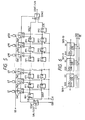
- the scan circuit includes AND gates, which are provided in a number that is equivalent to the count of the output lines, select switches SW1, two-stage delay flip-flops (D flip-flops) FF1 and FF2, and select switches SSW1 and SSW2.
- Fig. 6 is a diagram showing an example structure, for scan circuits of a single photoelectric converter, in which 10 scan circuit chips SR1-1 through SR1-10 are connected in series.
- Fig. 7 is a diagram showing the structure of a single integrated circuit detection chip.
- the IC chip includes a multiplexer, and employs a structure wherein an electric rotary switch for selecting the order for the output of received signals (or the order for the input of signals) is controlled by using a control signal input at a control terminal CONT.
- Fig. 8 is a diagram showing an example wherein 10 detection integrated circuit chips IC-1 through IC-10 are connected in series.
- the order in which the terminals of the chips that are connected to the gate lines or the signal lines of the photoelectric conversion device array are physically located, and the direction in which the chips are shifted are reversed.
- the shift directions for the IC chips shown in Figs. 5 through 8 are selectively determined in consonance with signals input at the control terminals DIR and CONT. IC chips of the same type can be mounted on both of the substrates 100 and 150.
- the scan circuits that are mounted on the upper left hand substrate 100 and the lower left hand substrate 150 are so determined that when a high voltage is applied to the terminal DIR the shift direction is toward the control lines g1, g2, ..., and g100.
- the scan circuits that are mounted on the upper right hand substrate 150 and the lower right hand substrate 100 are so determined that when a low voltage is applied to the terminal DIR the shift direction is toward the control lines g100, g99, ..., and g1.
- the scan select signals from the IC chips are output from the upper and lower left hand substrates in the order SR1-1 to SR1-10, while they are output from the upper and lower right hand substrates in the order SR1-10 to SR1-1.
- a high level pulse is input at the terminal CONT of the detection IC chips that are mounted on the upper right and left hand substrates in Fig. 3 , and detection signals are rearranged into a time series and are output from the terminals in the order sig1, sig2, ..., and sig100.
- a low level pulse is input at the terminals CONT of the detection IC chips that are mounted on the lower right and left hand substrates in Fig. 3 , and detection signals are rearranged into a time series and are output from the terminals in the order sig100, sig99, ..., and sig1.
- the outputs of the individual chips on the upper right and left hand substrates are performed in a time series in the order IC-1 to IC-10, while the outputs of the chips on the lower right and left hand substrates are performed in a time series in the order IC-10 to IC-1.
- IC chips There are four methods for mounting IC chips which can be employed for the photoelectric converter of the present invention. They are: a chip-on-glass system (COG method) for mounting chips directly on four substrates using a flip-chip system; a method (a TAB method) for employing a tape carrier package IC with which chips are connected to and mounted on a flexible printed wiring substrate; a wire bonding method for arranging IC chips on four substrates; and a monolithic integration method for fabricating scan circuits and detection circuits on the same substrate by using a thin semiconductor film that constitutes a photoelectric conversion device.
- COG method chip-on-glass system
- TAB method for employing a tape carrier package IC with which chips are connected to and mounted on a flexible printed wiring substrate
- wire bonding method for arranging IC chips on four substrates
- monolithic integration method for fabricating scan circuits and detection circuits on the same substrate by using a thin semiconductor film that constitutes a photoelectric conversion device.
- control lines or signal lines be connected to the terminals of a tape carrier package IC by using an anisotropic conductive adhesive.
- the four substrates can be laminated with a mothersubstrate having large dimensions that is made of glass, ceramic, metal or resin, and bonded together.
- Fig. 9 is a plan view of a photoelectric converter according to a second embodiment of the present invention.
- the same reference numerals as are used in Figs. 1 and 2 are also used in Fig. 3 to denote corresponding or identical components, and an explanation for them will be given only as needed.
- the feature of the photoelectric converter shown in Fig. 9 is that the substrates in at least one pair of the four substrates have different shapes.
- Fig. 9 a photoelectric converter having large dimensions in which a plane of a photoelectric conversion portion results in a rectangular shape for which four substrates are bonded together. That is, a pair or devices on substrates 50 that are diagonally located relative to each other have the same structure, while a pair of devices on substrates 250 that are diagonally located relative to each other have the same structure.
- the photoelectric conversion portion of a photoelectric converter having large dimensions that is obtained by bonding four substrates in a plane together may be shaped like a square. Taking ease of fabrication and manufacturing costs into consideration, however, the device shown in Fig. 9 is more preferable.
- the shape in a plane of the photoelectric conversion portion may be a rectangle, as in the second embodiment.
- paired substrates are so formed that each of them has the same pattern, and that on each of them the same scan circuits and detection integrated circuits are mounted.
- the resultant two substrates are rotated 180° and are bonded together with as small a gap as possible between them, so as to constitute a photoelectric converter having large dimensions.
- the inspection procedure can be performed by two types of devices, and the efficiency of the inspection procedure and the accompanying throughput can be increased. As a result, the cost of manufacturing a photoelectric converter having large dimensions can be reduced.
- the scan circuits and the detection integrated circuits that are mounted on the four substrates can be driven bidirectionally, and circuits can be employed for which the shift directions are determined by the input of signals specifying the shift directions, so that the four substrates arranged in Fig. 3 can be scanned in the same direction.
- a simple circuit is possible for processing read signals for all of the photoelectric conversion devices, and signals can be processed at a high speed. Therefore, a photoelectric converter having large dimensions and high performance can be provided at a low manufacturing cost.
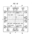
- Fig. 10 is a plan view of the overall structure of a photoelectric converter according to a third embodiment of the present invention.
- the reference numerals employed are those used to denote corresponding or identical components in Figs. 1 through 3 , and no explanation will be given for them.
- photoelectric conversion device arrays (shaded portions enclosed by broken lines) that are mounted on substrates 100, 200, 300 and 400 are arranged closely adjacent to each other, and are bonded together to constitute a single large photoelectric converter having large dimensions.
- each substrate 100 Located on each substrate 100 are 1000 ⁇ 1000 photoelectric devices that are connected to 2000 lines, i.e., 1000 control lines g1 through g1000 and 1000 signal lines sig1 through sig1000. And as there are 100 scan circuits formed on a single IC chip, there are a total of 10 IC chips SR1 through SR1-10 located on the substrate 100 and are connected to the respective control lines g1 through g1000.
- 100 processing circuits are integrated on a single IC chip, so that 10 IC chips, IC-1 through IC-10, are located on the substrate 100 and are connected to the signal lines sig1 through sig1000.
- the other substrates 200, 300 and 400 have the same structure as the substrate 100. Arranged on them are 1000 ⁇ 1000 photoelectric conversion devices that are connected to 1000 control lines and 1000 signal lines. Also provided are 10 of the scan circuits and 10 of the integrated detection circuits. Although these scan circuits and the integrated circuits may be same or may differ for each substrate, it is preferable that the above described ICs that can be driven bidirectionally be used for all the substrates.
- the four photoelectric conversion device arrays on the four substrates can be scanned at the same time. In this case, when compared with the example shown in Fig. 9 , the time period for the scanning can be reduced to 1/4 of that for the example shown in Fig. 9 .
- Fig. 11 is a diagram illustrating the arrangement of substrates in a plasma CVD device for fabricating a photoelectric converter according to the third embodiment of the present invention.
- the additional feature of the photoelectric converter in Fig. 10 is that the direction in which substrates 101, 201, 301 and 401, which respectively constitute the photoelectric converters 100, 200, 300 and 400 shown in Fig. 11 , are arranged in the plasma CVD device is the same as the direction in which the photoelectric converters 100, 200, 300 and 400 are arranged.
- the substrates 101, 201, 301 and 401 are so arranged that their corners pp face the center.
- tools 500 are employed to hold the substrates, and virtual cut lines 600 are employed along which the substrates are cut after thin film is deposited thereon.
- the film deposition speed tends to vary at the center of the substrates and at the center of the electrodes.
- an amorphous semiconductor layer such as an amorphous silicon layer, is deposited on the four substrates as arranged shown in Fig. 11 , and the substrates are bonded together in the illustrated direction.
- the characteristics of the photoelectric conversion devices at the seams of the four photoelectric converters are sequentially equalized, and as a result, a photoelectric converter that has large dimensions and has high performance can be provided.
- photoelectric conversion devices each of which is a lamination of a first electrode layer 2, an insulating layer 7, a semiconductor layer 4, a semiconductor layer 5 for preventing introduction of a first conductive carrier, and a second electrode layer 6.
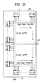
- Fig. 12 is a plan view of a photoelectric converter according to a fourth embodiment of the present invention.
- the same reference numerals as are used in Figs. 1 and 2 are also used in Fig. 3 to denote corresponding or identical components, and an explanation for them will be given only as needed.
- the feature of the photoelectric converter shown in Fig. 12 is that photoelectric converters 100 and 400 are bonded together with as small a gap as possible between them to constitute a single, large photoelectric converter.
- amorphous silicon is deposited on the photoelectric converters 100 and 400 that are arranged as is shown in Fig. 11 for the plasma CVD device.
- amorphous silicon is deposited on the substrates that are arranged as in Fig. 11 .
- the two substrates are bonded together as is shown in Fig. 12 so that the corners PP of the substrates 101 and 401 are aligned, and the photoelectric converter having large dimensions is thus fabricated.
- the characteristics of the photoelectric conversion devices at the seams of the two photoelectric converters become sequentially equal, and a photoelectric converter having large dimensions and a high performance can be produced.
- the two photoelectric converters that are arranged as is shown in Fig. 12 can be scanned in the direction indicated by the arrows in Fig. 12 .
- an X-ray machine in which a fluoresent member is provided on the photoelectric conversion device in the first to the fourth embodiment.
- the basic structure on the substrate is one wherein a light emitting layer that absorbs a high energy beam and generates visual radiation is provided on the light entering side in Fig. 5 .
- This structure is shown in Fig. 13 .
- a fluoresent member is deposited as a light-emitting element on a passivated film SiN.
- the fluor may be composed of cesium iodide (CsI), and generate fluorescence when struck by an X-ray.
- CsI cesium iodide
- the light-receiving device performs photoelectric conversion of the fluorescence.
- an X-ray detector of 40 cm ⁇ 40 cm can be acquired.
- a combination of this detector, which replaces an X-ray film, and an X-ray generator constitutes an X-ray machine that can be used for roentgen screening of breasts, or for examinations for mammary cancer.
- this X-ray detector can immediately display its output on a CRT, and the output can also be converted into digital output, for which image processing is performed by a computer, so that the output can be converted into an output that is consonant with the purpose of the device.
- the output data can be stored on a magneto-optical disk, and a quick search for previous images can be performed.
- the sensitivity of the detector is better than that of film, and a clear image can be provided by using an X-ray that has less adverse effect on a human body.
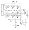
- Figs. 14 and 15 there are three scan lines for scan circuits on a single chip, while there are three data lines for the integrated detection circuits on a single chip, and a photoelectric conversion device array having a 3 ⁇ 3 matrix that can be driven is employed.
- a photoelectric conversion device array having a 3 ⁇ 3 matrix that can be driven is employed.
- Fig. 14 is a circuit diagram for explaining a method for driving a photoelectric converter according to the present invention.
- the structure of individual photoelectric conversion devices (pixels) is the same as that shown in Fig. 4A, 4B , 5 , or 13 .
- S11 through S33 denote light-receiving devices, each of which has a lower electrode G and an upper electrode D.
- Reference numerals C11 through C33 denote storage capacitors; and T11 through T33, transfer TFTs.
- a reading power source is denoted by Vs and a refresh power source is denoted by Vg.
- the power sources Vs and Vg are connected to the electrodes G of all the photoelectric conversion devices S11 through S33 via switches SWs and SWg.
- the switch SWs is connected to a refresh controller RF via an inverter, while the switch SWg is connected directly to the refresh controller RF.
- the refresh controller RF renders switch SWg on during a refresh period.
- One pixel is constituted by one light-receiving device, a capacitor and a TFT, and its output signal is transmitted to a detection integrated circuit IC across a signal line SIG.
- Fig. 14 The portion that is enclosed by broken lines in Fig. 14 is formed on the same insulating substrate having large dimensions.
- Fig. 15 is a timing chart showing the operation in Fig. 14 .
- a high level pulse is applied to control lines g1 through g3 and s1 through s3 by the scan circuits SR1 and SR2.
- the transfer TFTs T11 through T33, and switches M1 through M3 are rendered on and become conductive, and the electrodes D of all the light-receiving devices S11 through S33 acquire a GND potential as a reference potential because the input terminal of an integrating amplifier Amp is designed to be a GND potential.
- the refresh controller RF outputs a high level pulse and the SWg is turned on, the electrodes G of all the light-receiving devices S11 through S33 acquire a positive potential from the refresh power source Vg.
- all of the light-receiving devices S11 through S33 are placed in the refresh mode and are refreshed. Sequentially, when the refresh controller RF outputs a low level pulse and SWs is turned on, the electrodes G of all the light-receiving devices S11 through S33 acquire a negative potential from the reading power source Vs. The light-receiving devices S11 through S33 are placed in a photoelectric conversion mode, and at the same time, the capacitors C11 through C33 are initialized. While the device is in this condition, a low level pulse is applied to the control lines g1 through g3 and s1 through s3 by the scan circuits SR1 and SR2.
- the transfer TFTs T11 through T33 and the switches M1 through M3 are rendered off, and the electrodes D of all the light-receiving devices S11 through S33 are opened, but with their potentials being held by the capacitors C11 through C33.
- a high level control pulse is applied to the control line g1 by the scan circuit SR1, and a control pulse is applied to the control lines s1 through s3 by the scan circuit SR2.
- v1 through v3 are sequentially output via the switches M1 through M3 for the transfer TFTs T11 through T33.
- the other light signals are sequentially output under the control of the scan circuits SR1 and SR2.
- Two-dimensional photo data are converted into electric signals v1 through v9.
- a static image is obtained by performing the above processing, while a moving image is obtained by repeating the above processing.
- a combination of the photoelectric converter of the present invention and an X-ray generator can constitute an innovative X-ray machine that can be used for roentgen screening of breasts and the examinations for mammary cancers.
- the output can be immediately displayed on a CRT, and the output can also be converted into digital output, for which image processing is performed by a computer, so that the output can be converted into an output that is consonant with the purpose for which intended.
- the output data can be stored on a magneto-optical disk, and a search for previous images can be instituted without delay.
- the sensitivity provided is better than that for film, and a clear image can be provided by using an X-ray has less adverse effect on a human body.
- a photoconductive device or a photovoltaic device is employed as the light-receiving device for the photoelectric converter of the present invention.
- the photoelectric conversion device shown in Fig. 4A, 4B , 5 or 13 is preferable.
- Figs. 16A through 16C are diagrams illustrating the structure of a photosensor that servers as a light-receiving device.
- Figs. 16A and 16B are diagrams illustrating the structure of the layers of two types of photosensors, and Fig. 16C is a diagram showing a typical, commonly used driving system.
- the photosensors in Figs. 16A and 16B are photosensors of a photodiode type; the photosensor in Fig. 16A being called a PIN diode and the photosensor in Fig. 16B being called a Schottky diode.
- reference numeral 1 denotes an insulating substrate; 2, a lower electrode; 3, a p semiconductor layer (hereinafter referred to as a p layer); 4, an intrinsic semiconductor layer (hereinafter referred to as an i layer); 5, an n semiconductor layer (hereinafter referred to as an n layer); and 6, a transparent electrode.
- a Schottky diode in Fig. 16B the material that is correct for the lower electrode 2 is selected, and a Schottky-barrier layer is formed so that electrons from the lower electrode 2 are not introduced into the i layer 4.
- reference numeral 10 denotes the above described photosensor that is represented by using a symbol; 11, a power source; and 12, a detector, such as a current amplifier.
- C denotes the transparent electrode 6 side in Figs. 16A and 16B
- A denotes the lower electrode 2 side.
- the power source 11 is so set that when a positive voltage is applied at side A it is transmitted to side C.
- Figs. 16A and 16B when light enters in the direction indicated by an arrow and reaches the i layer 4, the light is absorbed and electrons and hole carriers are generated. Since an electric field is applied to the i layer 4 by the power source 11, the electrons pass through the side C, i.e., the n layer 5, and move to the transparent electrode 6, while the hole carriers are shifted to the side A, i.e., to the lower electrode 2. As a result, a photocurrent flows across the photosensor 10. When no light enters, electrons and hole carriers are not generated in the i layer 4.
- the n layer 5 serves as a layer for preventing the introduction of hole carriers into the transparent electrode 6. In the PIN photosensor in Fig.
- the p layer 3 serves as a layer for preventing the introduction of electrons into the lower electrode 2
- the Schottky-barrier layer serves as a layer for preventing the introduction of the electrons into the lower electrode 2. Therefore, the electrons and the hole carriers can not be moved and no current flows. Therefore, a current is varied depending on whether or not light enters. When this is detected by the detector 12 in Fig. 16C , the entire structure operates as a photosensor.
- the PIN photosensor in Fig. 16A and the Schottky photosensor in Fig. 16B require introduction prevention layers at two places.
- the n layer 5, which is an introduction prevention layer must have such characteristics that when electrons are guided to the transparent electrode 6, that at the same time, hole carriers are prevented from being introduced into the i layer 4. If either characteristic is missing from the n layer 5, a photocurrent is reduced, or when light does not enter, a current (hereinafter referred to as a dark current) is generated and increases, which results in the deterioration of an SN ratio.
- the dark current is itself considered as noise, and also includes fluctuation called Schottky noise, i.e., so-called quantum noise.
- the Schottky-barrier layer is employed as one of the introduction prevention layers, a difference between the work functions of the lower electrode 2 and the i layer 4 is utilized.
- the material for the lower electrode 2 is limited, and the local level for an interface greatly affects its characteristics, so that it is more difficult to satisfy the above described condition. It is reported that a thin oxide film or a nitride film of silicon or metal of around 100 angstroms can be deposited between the lower electrode 2 and the i layer 4 in order to enhance the characteristics of the Schottky-barrier layer.
- hole carriers are guided to the lower electrode 2 by utilizing the tunnel effect, and the effect for the prevention of the introduction of electrons into the i layer 4 is improved. Since a difference in the work functions is also employed by this method, the material employed for the lower electrode 2 must be limited. Further, since opposite properties, i.e., the prevention of the introduction of electrons and the shifting of the hole carriers by using the tunnel effect, are employed, the oxide film or the nitride film that is formed must be very thin, around 100 angstroms, and as control of the thickness and the film quality is difficult, productivity is degraded.
- the introduction prevention layer Since the introduction prevention layer must be deposited at two places, productivity is degraded and manufacturing costs are increased. Since the characteristics of the introduction prevention layer are important, a photosensor wherein a defect occurs in even one of these layers can not provide the characteristics required for a photosensor.
- Fig. 17 is a diagram illustrating the layered structure of a field-effect transistor (TFT) that is constituted by a thin semiconductor film.
- TFT field-effect transistor
- the TFT is sometime used as a part of a control section in order to fabricate a photoelectric converter.
- the same reference numerals as are used in Fig. 16 are also used to denote corresponding or identical layers.
- reference numeral 7 denotes an insulating film and 60 denotes an upper electrode. The deposition method will be sequentially described.
- a lower electrode 2 that serves as a gate electrode (G), a gate insulating film 7, an i layer 4, an n layer 5, and an upper electrode 60 that serves as a source electrode (S) and a drain electrode (D).
- Etching is performed on the upper electrode 60 to form the source electrode (S) and the drain electrode (D), and then etching is performed on the n layer 5 to form a channel portion. Since, as a characteristic of the TFT, it is sensitive to the condition of the interface between the gate insulating layer 7 and the i layer 4, generally, the above layers are sequentially formed in a vacuum to prevent contamination.
- the above described layer structure becomes a problem, and results in an increase in manufacturing costs and in the degrading of the characteristics.
- the structures of the photosensors in Figs. 16A to 16C and of the TFT are different; the structure of the PIN photosensor in Fig. 16A is an electrode/p layer/i layer/n layer/electrode lamination, and the structure of the Schottky photosensor in Fig. 16B is an electrode/i layer/n layer/electrode lamination, while the structure of the TFT is an electrode/insulating film/i layer/n layer/electrode lamination.
- the etching procedure for the gate insulating layer 7 and the p layer 3 is required in order to use the i layer/n layer in common.
- the p layer 3 and the i layer 4, which are the above described important introduction prevention layers for the photosensor, can not be deposited in the same vacuum, for the interface between the gate insulating film 7 and the i layer 4, which is important for the TFT, is contaminated when the gate insulating film is etched. As a result, the characteristics are deteriorated and the SN ratio is reduced.
- the oxide film or the nitride film must be so formed that it is around 100 angstroms, as is described above, and it is difficult to employ that film as the gate insulating film.
- Fig. 18 is a graph showing our experimental results for the gate insulating film and the yielding ratio for the TFT.
- a gate insulating film of 1000 angstroms or less the yielding ratio dropped drastically.
- the yielding ratio was about 30%; with a film of 500 angstroms, the yielding ratio was 0%; and with a film of 250 angstroms, it was not even possible to confirm the operation of the TFT.
- a capacity device hereafter referred to as a capacitor
- a capacitor which is a device that is required for obtaining the integral values of electric charges or of a current, to be fabricated so that it has the same structure as that of the photosensor, and so that it has a preferable characteristic for reducing leakage. Since the capacitor stores electric charges between two electrodes, a layer for preventing the movement of electrons and hole carriers must be formed as an intermediate layer between the electrodes. However, since the conventional photosensor uses only a semiconductor layer between the electrodes, it is difficult to obtain an intermediate layer that has a preferable characteristic for thermally reducing leakage.
- the processing and the characteristics of the TFT and the capacitor, which are important devices for a photoelectric converter, do not correspond with each other. Because of this problem, procedures are increased and are made more complicated for the fabrication of a system wherein a plurality of photosensors are two-dimensionally arranged and light signals are sequentially detected. This results in a deterioration of the yielding ratio, and prevents the production of a device having a low manufacturing cost and high performance and multiple functions.
- the photoelectric converter can be so driven that only for the photoelectric conversion device array on the upper right hand substrate 150, scanning and detection is performed, with no scanning and detection being performed for the other three substrates.
- signal detection can not be performed only for devices that are located at the intersections of the 100 control lines, g1, g2, ..., and g100, and the 100 signal lines sig1, sig2, ..., and sig100.
- signals are read from all the devices on the upper right hand substrate 150, and then only the required signals are reproduced.
- scan circuit chips and detection chips include a decoder, and a control line and a signal line to be selected are determined based on address data received from a controller, with only a terminal that is connected to these selected lines being selected.
- a photoelectric conversion device array is mounted on four substrates 710, 720, 730 and 740.
- Control lines are connected to 10 scan selector chips CP1, which are provided on each of the right and the left hand sides, and signal lines are connected to 10 detection IC chips CP2, which are provided on each of the upper and the down sides.
- a controller CRL selectively supplies, via wiring circuits DB1 and DB2, address data for a photoelectric device, which is to be selected for scanning, to chips CP1 and CP2 that have terminals which correspond to the address data.
- the chips CP1 or CP2 decode the data and enable the terminals that are to be selected. In this manner, a masking process is easily performed wherein only signals from a photoelectric conversion device that is located in a required region are reproduced.
- each chip has a decoder
- the scan selector chips having the same structure can be located on either the right or the left hand side. This can be applied for the IC detection chips.
- a plurality of control lines can be selected at the same time, or the chips can be selected for scanning by skipping a predetermined number of lines. This can be applied for the IC detection chips.
- a 40 cm ⁇ 40 cm array that is constituted by 2000 ⁇ 2000 photoelectric conversion devices is treated as a 400 ⁇ 400 array of 1 mm ⁇ 1 mm unit pixels (5 ⁇ 5 photoelectric conversion device group). Signals can be detected by sequentially scanning these unit pixels.
- the output signal of the unit pixels is an averaged value for 5 ⁇ 5 photoelectric conversion devices.
- the present invention it is possible to improve the throughput by providing improved efficiency on an inspection procedure that is performed during the fabrication of a photoelectric converter having large dimensions, and to reduce the total manufacturing cost by reducing the number of components.
- a photoelectric converter comprises a plurality of substrates, which are located adjacent to each other and on which a plurality of photoelectric conversion devices are two-dimensionally arranged, either scan circuits or detection circuits, at least, that are arranged on two opposing sides of the photoelectric converter, whereby scanning directions either from the scan circuits or from the detection circuits, which are arranged on the two opposing sides, are capable of being set so as to be performed in like directions.
Landscapes
- Engineering & Computer Science (AREA)
- Physics & Mathematics (AREA)
- Power Engineering (AREA)
- Computer Hardware Design (AREA)
- Condensed Matter Physics & Semiconductors (AREA)
- General Physics & Mathematics (AREA)
- Electromagnetism (AREA)
- Microelectronics & Electronic Packaging (AREA)
- Health & Medical Sciences (AREA)
- Toxicology (AREA)
- Signal Processing (AREA)
- Multimedia (AREA)
- Solid State Image Pick-Up Elements (AREA)
- Transforming Light Signals Into Electric Signals (AREA)
- Light Receiving Elements (AREA)
- Photometry And Measurement Of Optical Pulse Characteristics (AREA)
- Facsimile Heads (AREA)
Abstract
Description
- The present invention relates to a photoelectric converter, and in particular, to a two-dimensional photoelectric converter that is used for facsimile machines, digital copy machines, and X-ray machines.
- Conventionally, a scanning system that employs a reducing optical system and a CCD sensor is used for a scanning apparatus, such as a facsimile machine or a digital copy machine. Recently, however, as a consequence of the development of photoelectric conversion semiconductor material, such as amorphous silicon (hereinafter referred to as a-Si), a so-called close-contact sensor has been developed for which a photoelectric conversion device and a signal processor are formed on a large substrate, and by which data are scanned by using an optical system that has the same magnification rate as that of a data source. Furthermore, since a-Si can be employed not only as a photoelectric conversion material but also as a thin film field-effect transistor film (hereinafter referred to as a TFT), both a photoelectric conversion semiconductor layer and a TFT semiconductor layer can be formed at the same time.
- The basic structure of a photoelectric converter that uses a-Si is described in the specification for
USP 4,376,888 , or inJapanese Patent Publication No. 62-23944 Japanese Patent Publication No. 63-6617 - A specific example for the integral forming of an a-Si photosensor and an a-Si TFT is described in the specifications for
USP 4,931,661 ,USP 5,338,690 andUSP 5,306,648 . - Based on the techniques disclosed in these specifications, the present inventors produced as a sample photoelectric converter a two-dimensional area type in which the number of pixels was drastically increased. The outline of the photoelectric converter will now be described while referring to
Figs. 1 and2 . This device is disclosed inEuropean Patent Publication No. 0660421 . -
Figs. 1 and2 are plan views of a photoelectric converter that has 2000 × 2000 pixels. To provide 2000 × 2000 sensors, the number of photoelectric conversion devices that are included in an arrangement are increased in both the vertical and the horizontal directions. For this converter, 2000 control lines (scan lines) are also required, as is indicated by g1 through g2000, and accordingly, 2000 signal lines (data lines) are required, as is indicated by sig1 through sig2000. In addition, the sizes of a scanning circuit and an integrated circuit used for detection (a detection IC) are increased because they have to control and handle 2000 signal lines. When these processes are performed by single, one-chip ICs, the sizes of the chips must be increased, and the yielding manufacturing ratio and the prices are adversely affected. As is shown inFigs. 1 and2 , in a scan circuit, therefore, sufficient shift registers to handle 100 stages, for example, are formed on a single chip and 20 of these scan circuit chips (SR1-1 through SR1-20) are used. For the detection process for the integrated circuit, 100 processing circuits are formed on a single chip, and 20 of these integrated circuit detection chips (IC-1 through IC-20) are used. - In
Fig. 1 , 20 chips (SR1-1 through SR1-20) are mounted along the left side (L) and another 20 chips (IC-1 through IC-20) are mounted across the down side (D). Connected to each chip by wire bonding are 100 control lines or signal lines. The portion that is enclosed by broken lines inFig. 1 corresponds to a photoelectric conversion device array that is arranged as a two-dimensional area. The connection of the detection integrated circuit to an external device is not shown. - In another example, shown in
Fig. 2 ,10 chips (SR1-1 through SR1-10) are mounted along the left side (L) and 10 chips (SR1-11 through SR1-20) are mounted along the right side (R); and 10 chips (IC-1 through IC-10) are mounted across the upper side (U) and 10 chips (IC-11 through IC-20) are mounted across the down side (D). Since in thisstructure 1000 lines are provided at each of the upper, down, left and right sides (U, D, L and R), the density of the lines arranged along each side is reduced and the concentration of the wire bonding required on each side is also decreased, thus providing an increased manufacturing yielding ratio. Lines g1, g3, g5, ..., and g1999 are arranged along the left side (L), while g2, g4, g6, ..., and g2000 are arranged along the right side (R). That is, the odd numbered control lines are distributed along the left side (L), and the even numbered control lines are distributed along the right side (R). With this arrangement, since each line is pulled out so that the liens are located at equal intervals, the lines are not overly concentrated and the yielding ratio is increased. The wiring across the upper side (U) and the down side (D) is performed in the same manner. - Though not shown, in an additional example, lines g1 through g100, g201 through g300, ..., and g1801 through g1900 are provided on the left side (L), while lines g101 through g200, g301 through g400, ..., and g1901 through g2000 are provided on the right side (R). In other words, it is possible for contiguous control lines to be distributed to each chip and for these chips to be alternately sorted to the left side and to be right side (to L and to R). With this arrangement, the control lines for a single chip can be controlled sequentially, the adjustment and the setup of drive timing can be facilitated, a circuit does not become complicated, and an inexpensive IC can be used. The same arrangement can be applied for upper and the down sides (U and D), and an inexpensive IC that can perform a continuous process can be used.
- During the manufacturing process for a photoelectric converter having large dimensions, however, it is difficult to completely remove minute dust particles; it is especially difficult to remove a contaminant that is peeled off the wall of a thin film deposition device before a semiconductor layer, such as an amorphous layer, is deposited on a substrate, and it is also difficult to remove dust that remains on a substrate before a metal layer is deposited on the substrate. Therefore, it is difficult to eliminate wiring defects, i.e., short circuits or open circuits in lines.
- When the short circuits or open circuits in the control lines or the signal lines occur in a photoelectric converter having large dimensions, all of the output signals of the photoelectric converter devices that are connected to the short-circuited are rendered inexact, and the converter can not function as a photoelectric converter.
- In other words, as the size of one substrate is increased for the fabrication of a photoelectric converter having large dimensions, losses due to defects that occur during the manufacture of a substrate are also increased.
- Further, if the selection of control lines (scanning) is so designed that it is performed in the order corresponding to the direction indicated by arrow AL1 in
Fig. 2 , the order in which the output terminals for each of the scan circuits SR1-1 through SR1-10 are arranged on the left side (L) inFig. 2 is the opposite of the order in which the output terminals for each of the scan circuits SR1-11 through SR1-20 are arranged on the right side (R). When the scan circuits that are arranged on both sides are formed by using IC chips having the same structure, connection lines (lines for connecting control lines to the output terminals of the scan circuits) on either the right side (R) or the left side (L) must be formed of multi-layer lines, etc. As a result, the structure of the connection lines becomes complicated and expensive, and the high-density mounting of scan circuits is prevented. - Two types of ICs are prepared for which the orders in which output terminals are located differ, and ICs of one type are arranged on the left side (L), while ICs of the other type are arranged on the right side (R). However, the manufacture of two types of ICs, even though their basic operations are the same, results in higher manufacturing costs.
- The above described shortcomings not only apply to scan circuits, but also apply to detection ICs (IC-1 through IC-20) for the output of read signals in a time series.
- It is, therefore, a first object of the present invention to reduce a manufacturing costs for a photoelectric converter having large dimensions by providing an increased yielding ratio for each substrate during fabrication of photoelectric converter having large dimensions, and by reducing losses due to defects in each substrate.
- It is a second object of the present invention to provide better throughput to accompany an improved efficiency for an inspection procedure during fabrication of photoelectric converters having large dimensions, and to reduce total manufacturing costs that accompany a reduction in the number of components.
- It is a third object of the present invention to provide an enhanced function for a photoelectric converter having large dimensions by scanning all of the photoelectric conversion devices in the same direction, and by simplifying signal processing.
- It is a fourth object of the present invention to provide a photoelectric converter wherein one type of IC can be easily mounted on all sides, upper, down, right and left (U, D, R and L), of a photoelectric conversion device array.
- To achieve the above objects, according to a first aspect of the present invention, a photoelectric converter comprises:
- a plurality of substrates, which are located adjacent to each other and on which a plurality of photoelectric conversion devices are two-dimensionally arranged;
- either scan circuits or detection circuits, at least, that are arranged on two opposing sides of the photoelectric converter, whereby scanning directions either from the scan circuits or from the detection circuits, which are arranged on the two opposing sides, are capable of being set so as to be performed in like directions.
- Furthermore, to achieve the above objects according to a second aspect of the present invention, provided is a photoelectric converter wherein four substrates on which a plurality of photoelectric conversion devices are arranged two-dimensionally are so bonded together two-dimensionally, with two each in a vertical direction and in a horizontal direction, that the photoelectric conversion devices are located adjacent to each other on a plane; wherein, from among the four substrates that are bonded together, two substrates that are not adjacent to each other have such a positional relationship that substrates having the same structure are rotated 180° relative to each other on a plane; and wherein the substrates are scanned in the same direction.
- According to a third aspect of the present invention, provided is a photoelectric converter wherein a plurality of substrates, on which photoelectric conversion devices are two-dimensionally mounted, are so located and bonded together that the photoelectric conversion devices are located adjacent to each other on a plane; and wherein the plurality of substrates are bonded together at the same locations as those when semiconductor layers are deposited that serve as the photoelectric conversion devices for each of the substrates.
- Since a yielding ratio for each substrate during the fabrication process can be increased and losses due to defects on the substrates are reduced, the cost of manufacturing a photoelectric converter having large dimensions can be reduced.
- Further, as it is possible to improve the efficiency of an inspection procedure and the throughput that accompanies it, and to reduce the number of required components, and as a result, the cost of manufacturing a photoelectric converter having large dimensions can be reduced.
- In addition, since all of the photoelectric conversion devices can be scanned in the same direction and signal processing can be performed at a high speed by a simple device, the cost of manufacturing the photoelectric converter can be reduced, while the function of the photoelectric converter can be improved.
- Furthermore, a photoelectric converter wherein the amount of incident light can be detected, as the photoelectric conversion device has only one introduction prevention layer, can be provided at a low price; the optimizing of the process is easy and the yielding ratio can be increased; the manufacturing cost can be reduced; and the SN ratio is high.
- The exposure apparatus that employs the above converter differs from conventional X-ray film in that it can project its output very quickly, and in that image processing and data storage are also possible. It has better sensitivity than the film, and a clear image can be obtained with a weak X-ray that will have little adverse effect on a human body.
- When the substrates are bonded in consonance with the locations of the substrates when the film is deposited, the characteristics of the photoelectric conversion devices on different substrates that are at the least located at positions adjacent to each other on different substrates can be sequentially equalized.
-
-
Fig. 1 is a plan view of a conventional photoelectric converter that has 2000 × 2000 pixels; -
Fig. 2 is a plan view of another conventional photoelectric converter that has 2000 × 2000 pixels; -
Fig. 3 is a plan view of the overall structure of a photoelectric converter according to a first embodiment of the present invention; -
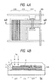
Fig. 4A is a cross sectional view of a photoelectric conversion device according to the first embodiment of the present invention; -
Fig. 4B is a cross sectional view of the scan structure taken alongline 4B - 4B inFig. 4A ; -
Fig. 5 is a diagram illustrating the structure of the scan circuits shown inFig. 3 ; -
Fig. 6 is a diagram showing an example structure of the scan circuits for a single photoelectric converter in which 10 scan circuit chips SR1-1 through SR1-10 are connected in series; -
Fig. 7 is a diagram showing the structure of a single integrated circuit detection chip; -
Fig. 8 is a diagram showing an example wherein 10 detection integrated circuit chips IC-1 through IC-10 are connected in series; -
Fig. 9 is a plan view of a photoelectric converter according to a second embodiment of the present invention; -
Fig. 10 is a plan view of the overall structure of a photoelectric converter according to a third embodiment of the present invention; -
Fig. 11 is a diagram illustrating the arrangement of substrates in a plasma CVD device for fabricating a photoelectric converter according to the third embodiment of the present invention; -
Fig. 12 is a plan view of a photoelectric converter according to a fourth embodiment of the present invention; -
Fig. 13 is a cross sectional view of a structure according to a fifth embodiment of the present invention wherein a fluoresence member is provided on the photoelectric conversion device in the first to the fourth embodiment; -
Fig. 14 is a circuit diagram for explaining a method for driving a photoelectric converter according to the present invention; -
Fig. 15 is a timing chart showing the operation inFig. 14 ; -
Fig. 16A is a diagram illustrating the structure of the layers of a PIN photosensor; -
Fig. 16B is a diagram illustrating the structure of the layers of a Schottky photosensor; -
Fig. 16C is a diagram illustrating a typical commonly used driving system; -
Fig. 17 is a diagram illustrating the layer structure of a field-effect transistor (TFT) that is constituted by a thin semiconductor film; -
Fig. 18 is a graph showing our experimental results for an gate insulating film and a yielding ratio for the TFT; and -
Fig. 19 is a diagram illustrating photoelectric conversion device arrays that are mounted on four substrates. -
Fig. 3 is a plan view of the overall structure of a photoelectric converter according to a first embodiment of the present invention. The reference numerals are used to denote corresponding or identical components inFigs. 1 and2 , and no explanation will be given for them. - As the feature of the photoelectric converter shown in
Fig. 3 , while each pair of foursubstrates - Two diagonally located substrates have the same structures.
- Further, when the scanning direction, indicated by arrows in
Fig. 3 , for the scan circuits of the photoelectric device arrays on the four substrates and the scanning direction, also indicated by arrows inFig. 3 for their detection integrated circuits, i.e., the directions for the parallel-serial conversion of detection signals, are set to be bidirectional, the four photoelectric conversion device arrays are scanned in the same direction as when viewed as a whole, which is the feature of the photoelectric converter. - Located on each
substrate 100 are 1000 x 1000 photoelectric devices that are connected to 2000 lines, i.e., 1000 control lines g1 through g1000 and 1000 signal lines sig1 through sig1000. And as there are 100 scan circuits SR1 formed on a single IC chip, there are a total of 10 IC chips SR1 through SR1-10 located on thesubstrate 100, the individual terminals of each IC chip being connected to the respective control lines g1 through g1000. - As for the detection integrated circuits, 100 processing circuits are formed on a single IC chip, with 10 detection integrated circuit chips, IC-1 through IC-10, being located on each substrate and with the individual terminals of each IC chip being connected to the signal lines sig1 through sig1000. The
substrate 150 has the same structured as thesubstrate 100, and has 1000 x 1000 photoelectric conversion devices arranged on it that are connected to 1000 control lines and 1000 signal lines. Also provided are 10 of the scan circuits and 10 of the detection integrated circuits. Although for each substrate these scan circuits and the integrated circuits may differ, it is preferable that a single type of IC be used for all the substrates, as will be described later. Thus, the four photoelectric conversion device arrays on the four substrates can be scanned at the same time. In this case, when compared with the example shown inFig. 2 , the period of time required for the scanning can be reduced to 1/4 of that required for the example inFig. 2 . - The photoelectric device arrays are fabricated on the four substrates, as is shown in
Fig. 3 , and the four substrates are bonded together with as a small gap as possible between them, so that a photoelectric converter having large dimensions can be constituted. As a result, the yielding ratio for each substrate can be increased, and the losses that are incurred due to defects on the individual substrates can be reduced. - Specifically, when the area of the photoelectric converter in
Fig. 3 on which photoelectric conversion devices are mounted is the same as the area of the photoelectric converter inFig. 1 on which photoelectric conversion devices are mounted, the total length of all of the control lines and all of the signal lines for the substrates inFig. 3 is about 1/4 the total length of all the control lines and signal lines for the photoelectric converter inFig. 1 . - In such a photoelectric converter, a short circuit or an open circuit in a control line or in a signal line causes all of the output signals of the photoelectric conversion devices connected to the line to become inaccurate, and the photoelectric converter can not be employed. The possibility of the occurrence of such a defect is substantially proportional to the total length of all the control lines and signal lines, and as a result of such a defect, the yielding ratio will be reduced.
- Therefore, a yielding ratio due to a defect in the wiring for each substrate in
Fig. 3 is about four times the yielding ratio for the photoelectric converter shown inFig. 1 . The loss that is occasioned when a defect occurs on one substrate shown inFig. 3 and the photoelectric converter can not be used is proportionate to the dimensions of all the substrates. The loss, therefore, is about 1/4 of that experienced as a loss by the photoelectric converter inFig. 1 when a defect occurs and the converter can not be used. - As is shown in
Fig. 3 , two of thesubstrates 100 are formed that have a first pattern photoelectric conversion device array, while two of thesubstrates 150 are formed that have a second pattern photoelectric conversion device array, and mounted on these four substrates are the same scan circuits and detection integrated circuits. Two of the substrates are rotated 180° and are diagonally positioned, and the four substrates are bonded together to constitute a photoelectric converter having large dimensions. As a result, the number of required components can be reduced. The inspection procedure can be performed by two types of devices, and the efficiency of the inspection procedure and accompanying throughput can be increased. As a result, the cost of manufacturing a photoelectric converter having large dimensions can be reduced. - The scan circuits and the integrated detection circuits, which are mounted on the four substrates, can be driven bidirectionally, and the circuits are employed in the shift direction that is determined by the input of a signal for specifying the shift direction, so that the four substrates arranged in
Fig. 3 can be scanned in the same direction. As a result, a simple circuit is required for processing read signals for all of the photoelectric conversion devices, and signals can be processed at a high speed. - Therefore, a photoelectric converter having large dimensions and high performance can be provided at a low manufacturing cost.
- As is shown in
Figs. 4A and 4B , provided as the structure on the photoelectric converter are photoelectric conversion devices, each of which is a laminate composed of afirst electrode layer 2, an insulatinglayer 7, asemiconductor layer 4 that can perform photoelectric conversion, asemiconductor layer 5 for preventing introduction of a first conductive carrier, and asecond electrode layer 6. The photoelectric converter comprises: photoelectric conversion means for accumulating, on thesemiconductor layer 5, the first conductive carrier, which is induced by signal light that enters thesemiconductor layer 5, and for providing an electric field to a light receiving device in a direction in which the second conductive carrier, which differs from the first conductive carrier, is to be guided to thesecond electrode layer 6; refresh means for providing an electric field for the light receiving devices in a direction in which the first conductive carrier is to be guided from the semiconductor layer to the second electrode layer; and a signal detector for detecting the first conductive carrier, which is accumulated on the semiconductor layer, or the second conductive carrier, which is guided to the second electrode layer, during photoelectric conversion performed by the photoelectric conversion means. - In
Figs. 4A, 4B and5 , S11 denotes a light-receiving device; T11, a TFT; C11, a capacitor, and SIG, a signal line. The capacitor C12 and the light-receiving device S11 are not separated from each other, and they can be integrally formed because the light-receiving device, the capacitor and the TFT have substantially the same layer structure. A silicon nitride film SiN is deposited as a passivated film on the upper portion of a pixel. When light enters the photoelectric conversion device from upward, the light is converted into an electric signal (accumulated electric change amount). - The structure of the scan circuit shown in
Fig. 3 will now be explained while referring toFig. 5 . - The scan circuit includes AND gates, which are provided in a number that is equivalent to the count of the output lines, select switches SW1, two-stage delay flip-flops (D flip-flops) FF1 and FF2, and select switches SSW1 and SSW2.
- When a high level voltage is applied, as a signal for specifying a shift direction, to terminal DIR, the select switches SSW1, SSW2 and SW1 are shifted to high (H). In consonance with a shift pulse, which is input at input/output terminal SIN/SOUT on the left side (L20) in
Fig. 5 , and a clock, which is input at a clock input terminal, the D flip-flops FF1 sequentially output a series of "1s", indicating which gate lines are selected, to the AND gates via the select switches SW1. When, at this time, an output-enable pulse "1" is input at control terminal OE, the output of the AND gates is "1" and an output terminal is selected. In this manner, the output terminals are selected in the order g1, g2, g3, ..., g98, g99, and g100. - The operation for performing shift in the opposite direction will now be described. When a low level voltage is applied in the shift direction to control terminal DIR, the select switches SSW2, SW1 and SSW1 are shifted to low (L).
- When a shift pulse is input at the input/output terminal SOUT/SIN on the right side (R) in
Fig. 5 , the D flip-flops FF2 sequentially output a series of "1s" to the AND gates via the select switches SW1. When, at this time, an output enable pulse "1" is input at the control terminal OE, the output of the AND gates is "1" and an output line is selected. In this manner, the output lines are selected in the order g100, g99, g98, ..., g3, g2, and g1. -
Fig. 6 is a diagram showing an example structure, for scan circuits of a single photoelectric converter, in which 10 scan circuit chips SR1-1 through SR1-10 are connected in series.Fig. 7 is a diagram showing the structure of a single integrated circuit detection chip. The IC chip includes a multiplexer, and employs a structure wherein an electric rotary switch for selecting the order for the output of received signals (or the order for the input of signals) is controlled by using a control signal input at a control terminal CONT. -
Fig. 8 is a diagram showing an example wherein 10 detection integrated circuit chips IC-1 through IC-10 are connected in series. - The operation performed by the converter in
Fig. 3 , for which the scan circuits and the detection integrated circuits shown inFigs. 5 through 8 are employed, will now be described. - Depending on whether a chip is mounted on the
substrate 100 or on thesubstrate 150, the order in which the terminals of the chips that are connected to the gate lines or the signal lines of the photoelectric conversion device array are physically located, and the direction in which the chips are shifted are reversed. - The shift directions for the IC chips shown in
Figs. 5 through 8 are selectively determined in consonance with signals input at the control terminals DIR and CONT. IC chips of the same type can be mounted on both of thesubstrates - The scan circuits that are mounted on the upper
left hand substrate 100 and the lowerleft hand substrate 150 are so determined that when a high voltage is applied to the terminal DIR the shift direction is toward the control lines g1, g2, ..., and g100. - On the other hand, the scan circuits that are mounted on the upper
right hand substrate 150 and the lowerright hand substrate 100 are so determined that when a low voltage is applied to the terminal DIR the shift direction is toward the control lines g100, g99, ..., and g1. - The scan select signals from the IC chips are output from the upper and lower left hand substrates in the order SR1-1 to SR1-10, while they are output from the upper and lower right hand substrates in the order SR1-10 to SR1-1.
- Similarly, a high level pulse is input at the terminal CONT of the detection IC chips that are mounted on the upper right and left hand substrates in
Fig. 3 , and detection signals are rearranged into a time series and are output from the terminals in the order sig1, sig2, ..., and sig100. - On the other hand, a low level pulse is input at the terminals CONT of the detection IC chips that are mounted on the lower right and left hand substrates in
Fig. 3 , and detection signals are rearranged into a time series and are output from the terminals in the order sig100, sig99, ..., and sig1. - The outputs of the individual chips on the upper right and left hand substrates are performed in a time series in the order IC-1 to IC-10, while the outputs of the chips on the lower right and left hand substrates are performed in a time series in the order IC-10 to IC-1.
- There are four methods for mounting IC chips which can be employed for the photoelectric converter of the present invention. They are: a chip-on-glass system (COG method) for mounting chips directly on four substrates using a flip-chip system; a method (a TAB method) for employing a tape carrier package IC with which chips are connected to and mounted on a flexible printed wiring substrate; a wire bonding method for arranging IC chips on four substrates; and a monolithic integration method for fabricating scan circuits and detection circuits on the same substrate by using a thin semiconductor film that constitutes a photoelectric conversion device. When the size of an IC chip is too large to ignore and the size of the external region (external frame) of a photoelectric conversion device array is to be reduced, the use of the TAB method, with which a substrate can be bent, is preferable. According to the TAB method, it is preferable that control lines or signal lines be connected to the terminals of a tape carrier package IC by using an anisotropic conductive adhesive.
- The four substrates can be laminated with a mothersubstrate having large dimensions that is made of glass, ceramic, metal or resin, and bonded together.
-
Fig. 9 is a plan view of a photoelectric converter according to a second embodiment of the present invention. The same reference numerals as are used inFigs. 1 and2 are also used inFig. 3 to denote corresponding or identical components, and an explanation for them will be given only as needed. - The feature of the photoelectric converter shown in
Fig. 9 is that the substrates in at least one pair of the four substrates have different shapes. InFig. 9 is provided a photoelectric converter having large dimensions in which a plane of a photoelectric conversion portion results in a rectangular shape for which four substrates are bonded together. That is, a pair or devices onsubstrates 50 that are diagonally located relative to each other have the same structure, while a pair of devices onsubstrates 250 that are diagonally located relative to each other have the same structure. When a pair of substrates on a plane differ in shape, the photoelectric conversion portion of a photoelectric converter having large dimensions that is obtained by bonding four substrates in a plane together may be shaped like a square. Taking ease of fabrication and manufacturing costs into consideration, however, the device shown inFig. 9 is more preferable. - When the photoelectric converter of the present invention having large dimensions of the present invention is employed for an X-ray machine for human breasts, the shape in a plane of the photoelectric conversion portion may be a rectangle, as in the second embodiment.
- In this case, also, paired substrates are so formed that each of them has the same pattern, and that on each of them the same scan circuits and detection integrated circuits are mounted. The resultant two substrates are rotated 180° and are bonded together with as small a gap as possible between them, so as to constitute a photoelectric converter having large dimensions. As a result, the number of required components can be reduced. The inspection procedure can be performed by two types of devices, and the efficiency of the inspection procedure and the accompanying throughput can be increased. As a result, the cost of manufacturing a photoelectric converter having large dimensions can be reduced.
- The scan circuits and the detection integrated circuits that are mounted on the four substrates can be driven bidirectionally, and circuits can be employed for which the shift directions are determined by the input of signals specifying the shift directions, so that the four substrates arranged in
Fig. 3 can be scanned in the same direction. As a result, a simple circuit is possible for processing read signals for all of the photoelectric conversion devices, and signals can be processed at a high speed. Therefore, a photoelectric converter having large dimensions and high performance can be provided at a low manufacturing cost. -
Fig. 10 is a plan view of the overall structure of a photoelectric converter according to a third embodiment of the present invention. The reference numerals employed are those used to denote corresponding or identical components inFigs. 1 through 3 , and no explanation will be given for them. - As the feature of the photoelectric converter shown in
Fig. 10 , photoelectric conversion device arrays (shaded portions enclosed by broken lines) that are mounted onsubstrates - Located on each
substrate 100 are 1000 × 1000 photoelectric devices that are connected to 2000 lines, i.e., 1000 control lines g1 through g1000 and 1000 signal lines sig1 through sig1000. And as there are 100 scan circuits formed on a single IC chip, there are a total of 10 IC chips SR1 through SR1-10 located on thesubstrate 100 and are connected to the respective control lines g1 through g1000. - As for the integrated detection circuits, 100 processing circuits are integrated on a single IC chip, so that 10 IC chips, IC-1 through IC-10, are located on the
substrate 100 and are connected to the signal lines sig1 through sig1000. Theother substrates substrate 100. Arranged on them are 1000 × 1000 photoelectric conversion devices that are connected to 1000 control lines and 1000 signal lines. Also provided are 10 of the scan circuits and 10 of the integrated detection circuits. Although these scan circuits and the integrated circuits may be same or may differ for each substrate, it is preferable that the above described ICs that can be driven bidirectionally be used for all the substrates. The four photoelectric conversion device arrays on the four substrates can be scanned at the same time. In this case, when compared with the example shown inFig. 9 , the time period for the scanning can be reduced to 1/4 of that for the example shown inFig. 9 . -
Fig. 11 is a diagram illustrating the arrangement of substrates in a plasma CVD device for fabricating a photoelectric converter according to the third embodiment of the present invention. The additional feature of the photoelectric converter inFig. 10 is that the direction in whichsubstrates photoelectric converters Fig. 11 , are arranged in the plasma CVD device is the same as the direction in which thephotoelectric converters substrates - In
Fig. 11 ,tools 500 are employed to hold the substrates, andvirtual cut lines 600 are employed along which the substrates are cut after thin film is deposited thereon. - Since generally a device for a parallel flat plate that ejects gas through holes in one of its electrodes is employed as a plasma CVD device, the film deposition speed tends to vary at the center of the substrates and at the center of the electrodes. On the other hand, an amorphous semiconductor layer, such as an amorphous silicon layer, is deposited on the four substrates as arranged shown in
Fig. 11 , and the substrates are bonded together in the illustrated direction. In the thus fabricated photoelectric converter having large dimensions, the characteristics of the photoelectric conversion devices at the seams of the four photoelectric converters are sequentially equalized, and as a result, a photoelectric converter that has large dimensions and has high performance can be provided. - As is shown in
Figs. 4 and5 , on each of the substrates are provided photoelectric conversion devices, each of which is a lamination of afirst electrode layer 2, an insulatinglayer 7, asemiconductor layer 4, asemiconductor layer 5 for preventing introduction of a first conductive carrier, and asecond electrode layer 6. -
Fig. 12 is a plan view of a photoelectric converter according to a fourth embodiment of the present invention. The same reference numerals as are used inFigs. 1 and2 are also used inFig. 3 to denote corresponding or identical components, and an explanation for them will be given only as needed. - The feature of the photoelectric converter shown in
Fig. 12 is thatphotoelectric converters photoelectric converters Fig. 11 for the plasma CVD device. Thus, amorphous silicon is deposited on the substrates that are arranged as inFig. 11 . While maintaining this arrangement, the two substrates are bonded together as is shown inFig. 12 so that the corners PP of thesubstrates - Furthermore, as well as in the first through the third embodiments, since the scan circuits and detection integrated circuits that are mounted on the two substrates can be driven bidirectionally, the two photoelectric converters that are arranged as is shown in
Fig. 12 can be scanned in the direction indicated by the arrows inFig. 12 . - According to a fifth embodiment, provided is an X-ray machine in which a fluoresent member is provided on the photoelectric conversion device in the first to the fourth embodiment.
- The basic structure on the substrate is one wherein a light emitting layer that absorbs a high energy beam and generates visual radiation is provided on the light entering side in
Fig. 5 . This structure is shown inFig. 13 . A fluoresent member is deposited as a light-emitting element on a passivated film SiN. The fluor may be composed of cesium iodide (CsI), and generate fluorescence when struck by an X-ray. The light-receiving device performs photoelectric conversion of the fluorescence. When 2000 × 2000 pixels are arranged two-dimensionally, with, for example, 5 × 5 pixels per 1-mm square, an X-ray detector of 40 cm × 40 cm can be acquired. - A combination of this detector, which replaces an X-ray film, and an X-ray generator constitutes an X-ray machine that can be used for roentgen screening of breasts, or for examinations for mammary cancer. Unlike X-ray films, this X-ray detector can immediately display its output on a CRT, and the output can also be converted into digital output, for which image processing is performed by a computer, so that the output can be converted into an output that is consonant with the purpose of the device. The output data can be stored on a magneto-optical disk, and a quick search for previous images can be performed. The sensitivity of the detector is better than that of film, and a clear image can be provided by using an X-ray that has less adverse effect on a human body.
- The method for driving a photoelectric conversion device array that is employed for the present invention will now be explained while referring to
Figs. 14 and15 . In this case, there are three scan lines for scan circuits on a single chip, while there are three data lines for the integrated detection circuits on a single chip, and a photoelectric conversion device array having a 3 × 3 matrix that can be driven is employed. When 10 scan circuit chips and 10 detection integrated circuit chips are employed, and when 1000 scan lines and 1000 data lines are provided and the photoelectric conversion device is a 1000 × 1000 matrix, it is apparent that scanning and detection for a single substrate inFig. 3 can be performed. -
Fig. 14 is a circuit diagram for explaining a method for driving a photoelectric converter according to the present invention. The structure of individual photoelectric conversion devices (pixels) is the same as that shown inFig. 4A, 4B ,5 , or13 . - In
Fig. 14 , S11 through S33 denote light-receiving devices, each of which has a lower electrode G and an upper electrode D. Reference numerals C11 through C33 denote storage capacitors; and T11 through T33, transfer TFTs. A reading power source is denoted by Vs and a refresh power source is denoted by Vg. The power sources Vs and Vg are connected to the electrodes G of all the photoelectric conversion devices S11 through S33 via switches SWs and SWg. The switch SWs is connected to a refresh controller RF via an inverter, while the switch SWg is connected directly to the refresh controller RF. The refresh controller RF renders switch SWg on during a refresh period. One pixel is constituted by one light-receiving device, a capacitor and a TFT, and its output signal is transmitted to a detection integrated circuit IC across a signal line SIG. - The portion that is enclosed by broken lines in
Fig. 14 is formed on the same insulating substrate having large dimensions. -
Fig. 15 is a timing chart showing the operation inFig. 14 . - First, a high level pulse is applied to control lines g1 through g3 and s1 through s3 by the scan circuits SR1 and SR2. When the transfer TFTs T11 through T33, and switches M1 through M3 are rendered on and become conductive, and the electrodes D of all the light-receiving devices S11 through S33 acquire a GND potential as a reference potential because the input terminal of an integrating amplifier Amp is designed to be a GND potential. At the same time, when the refresh controller RF outputs a high level pulse and the SWg is turned on, the electrodes G of all the light-receiving devices S11 through S33 acquire a positive potential from the refresh power source Vg. Then, all of the light-receiving devices S11 through S33 are placed in the refresh mode and are refreshed. Sequentially, when the refresh controller RF outputs a low level pulse and SWs is turned on, the electrodes G of all the light-receiving devices S11 through S33 acquire a negative potential from the reading power source Vs. The light-receiving devices S11 through S33 are placed in a photoelectric conversion mode, and at the same time, the capacitors C11 through C33 are initialized. While the device is in this condition, a low level pulse is applied to the control lines g1 through g3 and s1 through s3 by the scan circuits SR1 and SR2. Then, the transfer TFTs T11 through T33 and the switches M1 through M3 are rendered off, and the electrodes D of all the light-receiving devices S11 through S33 are opened, but with their potentials being held by the capacitors C11 through C33.
- Since no light beam is received at this time, no light is transmitted to the light-receiving devices S11 through S33 and a photocurrent does not flow across them. In this condition, a light beam pulse is emitted and is transmitted to the light-receiving devices S11 through S33 via an object to be exposed. An induced photocurrent that flows due to this light is stored as electric charges in the capacitors C11 through C33, and the electric charges are held therein after the transmission of a light beam has been completed.
- Following this, a high level control pulse is applied to the control line g1 by the scan circuit SR1, and a control pulse is applied to the control lines s1 through s3 by the scan circuit SR2. Then, v1 through v3 are sequentially output via the switches M1 through M3 for the transfer TFTs T11 through T33. Similarly, the other light signals are sequentially output under the control of the scan circuits SR1 and SR2. Two-dimensional photo data are converted into electric signals v1 through v9. A static image is obtained by performing the above processing, while a moving image is obtained by repeating the above processing.
- In this photoelectric converter, since the electrodes G of the light-receiving devices are connected in common, and the line that is used in common is connected to both the refresh power source Vg and the reading power source Vs via the switches SWg and SWs, respectively, to control the potentials of the electrodes G, all of the light-receiving devices can be switched to the refresh mode and to the photoelectric conversion mode at the same time. Therefore, light output can be obtained by using one TFT for each pixel and without requiring a complicated control system.
- Instead of the X-ray film that is used in a conventional X-ray machine, a combination of the photoelectric converter of the present invention and an X-ray generator can constitute an innovative X-ray machine that can be used for roentgen screening of breasts and the examinations for mammary cancers. Unlike the X-ray film, the output can be immediately displayed on a CRT, and the output can also be converted into digital output, for which image processing is performed by a computer, so that the output can be converted into an output that is consonant with the purpose for which intended. The output data can be stored on a magneto-optical disk, and a search for previous images can be instituted without delay. The sensitivity provided is better than that for film, and a clear image can be provided by using an X-ray has less adverse effect on a human body.
- A photoconductive device or a photovoltaic device is employed as the light-receiving device for the photoelectric converter of the present invention. For a reason that will be described later, however, the photoelectric conversion device shown in
Fig. 4A, 4B ,5 or13 is preferable. -
Figs. 16A through 16C are diagrams illustrating the structure of a photosensor that servers as a light-receiving device.Figs. 16A and 16B are diagrams illustrating the structure of the layers of two types of photosensors, andFig. 16C is a diagram showing a typical, commonly used driving system. The photosensors inFigs. 16A and 16B are photosensors of a photodiode type; the photosensor inFig. 16A being called a PIN diode and the photosensor inFig. 16B being called a Schottky diode. - In
Figs. 16A and 16B ,reference numeral 1 denotes an insulating substrate; 2, a lower electrode; 3, a p semiconductor layer (hereinafter referred to as a p layer); 4, an intrinsic semiconductor layer (hereinafter referred to as an i layer); 5, an n semiconductor layer (hereinafter referred to as an n layer); and 6, a transparent electrode. In the Schottky diode inFig. 16B , the material that is correct for thelower electrode 2 is selected, and a Schottky-barrier layer is formed so that electrons from thelower electrode 2 are not introduced into thei layer 4. InFig. 16C ,reference numeral 10 denotes the above described photosensor that is represented by using a symbol; 11, a power source; and 12, a detector, such as a current amplifier. At thephotosensor 10, C denotes thetransparent electrode 6 side inFigs. 16A and 16B , and A denotes thelower electrode 2 side. Thepower source 11 is so set that when a positive voltage is applied at side A it is transmitted to side C. - The processing will now be briefly described. As is shown in
Figs. 16A and 16B , when light enters in the direction indicated by an arrow and reaches thei layer 4, the light is absorbed and electrons and hole carriers are generated. Since an electric field is applied to thei layer 4 by thepower source 11, the electrons pass through the side C, i.e., then layer 5, and move to thetransparent electrode 6, while the hole carriers are shifted to the side A, i.e., to thelower electrode 2. As a result, a photocurrent flows across thephotosensor 10. When no light enters, electrons and hole carriers are not generated in thei layer 4. Then layer 5 serves as a layer for preventing the introduction of hole carriers into thetransparent electrode 6. In the PIN photosensor inFig. 16A , thep layer 3 serves as a layer for preventing the introduction of electrons into thelower electrode 2, while in the Schottky photosensor inFig. 16B , the Schottky-barrier layer serves as a layer for preventing the introduction of the electrons into thelower electrode 2. Therefore, the electrons and the hole carriers can not be moved and no current flows. Therefore, a current is varied depending on whether or not light enters. When this is detected by thedetector 12 inFig. 16C , the entire structure operates as a photosensor. - It is, however, difficult for the above described photosensor to be employed to produce a photoelectric converter having a high SN ratio and a low manufacturing cost. An explanation of the reasons will now be given.
- The first reason is that the PIN photosensor in
Fig. 16A and the Schottky photosensor inFig. 16B require introduction prevention layers at two places. In the PIN photosensor inFig. 16A , then layer 5, which is an introduction prevention layer, must have such characteristics that when electrons are guided to thetransparent electrode 6, that at the same time, hole carriers are prevented from being introduced into thei layer 4. If either characteristic is missing from then layer 5, a photocurrent is reduced, or when light does not enter, a current (hereinafter referred to as a dark current) is generated and increases, which results in the deterioration of an SN ratio. The dark current is itself considered as noise, and also includes fluctuation called Schottky noise, i.e., so-called quantum noise. Even when a process for restricting a dark current is performed by thedetector 12, quantum noise that accompanies the dark current can not be reduced. In order to improve the characteristics normally, generally the conditions for forming thei layer 4 and then layer 5, and the annealing conditions after the photosensor is fabricated, must be optimized. Thep layer 3, another introduction projection layer, requires the same characteristics, even though it prevents the introduction of electrons, not hole carriers, and the above described conditions for this layer must also be optimized. Normally, the conditions for optimization of the n layer and those for the p layer are not the same, and thus it is difficult to satisfy the conditions for both. In other words, it is difficult to fabricate a photosensor having a high SN ratio for which an introduction prevention layer is required at two places. - The same principle can be applied to the Schottky photosensor in
Fig. 16B . Further, although for the Schottky type inFig. 16B the Schottky-barrier layer is employed as one of the introduction prevention layers, a difference between the work functions of thelower electrode 2 and thei layer 4 is utilized. The material for thelower electrode 2 is limited, and the local level for an interface greatly affects its characteristics, so that it is more difficult to satisfy the above described condition. It is reported that a thin oxide film or a nitride film of silicon or metal of around 100 angstroms can be deposited between thelower electrode 2 and thei layer 4 in order to enhance the characteristics of the Schottky-barrier layer. According to this, hole carriers are guided to thelower electrode 2 by utilizing the tunnel effect, and the effect for the prevention of the introduction of electrons into thei layer 4 is improved. Since a difference in the work functions is also employed by this method, the material employed for thelower electrode 2 must be limited. Further, since opposite properties, i.e., the prevention of the introduction of electrons and the shifting of the hole carriers by using the tunnel effect, are employed, the oxide film or the nitride film that is formed must be very thin, around 100 angstroms, and as control of the thickness and the film quality is difficult, productivity is degraded. - Since the introduction prevention layer must be deposited at two places, productivity is degraded and manufacturing costs are increased. Since the characteristics of the introduction prevention layer are important, a photosensor wherein a defect occurs in even one of these layers can not provide the characteristics required for a photosensor.
- The second reason will now be described while referring to
Fig. 17. Fig. 17 is a diagram illustrating the layered structure of a field-effect transistor (TFT) that is constituted by a thin semiconductor film. The TFT is sometime used as a part of a control section in order to fabricate a photoelectric converter. The same reference numerals as are used inFig. 16 are also used to denote corresponding or identical layers. InFig. 17 ,reference numeral 7 denotes an insulating film and 60 denotes an upper electrode. The deposition method will be sequentially described. On an insulatingsubstrate 1 are sequentially deposited alower electrode 2 that serves as a gate electrode (G), agate insulating film 7, ani layer 4, ann layer 5, and anupper electrode 60 that serves as a source electrode (S) and a drain electrode (D). Etching is performed on theupper electrode 60 to form the source electrode (S) and the drain electrode (D), and then etching is performed on then layer 5 to form a channel portion. Since, as a characteristic of the TFT, it is sensitive to the condition of the interface between thegate insulating layer 7 and thei layer 4, generally, the above layers are sequentially formed in a vacuum to prevent contamination. - When a conventional photosensor is to be formed on the same substrate as the TFT, the above described layer structure becomes a problem, and results in an increase in manufacturing costs and in the degrading of the characteristics. This is because the structures of the photosensors in
Figs. 16A to 16C and of the TFT are different; the structure of the PIN photosensor inFig. 16A is an electrode/p layer/i layer/n layer/electrode lamination, and the structure of the Schottky photosensor inFig. 16B is an electrode/i layer/n layer/electrode lamination, while the structure of the TFT is an electrode/insulating film/i layer/n layer/electrode lamination. This means that the photosensor and the TFT can not be fabricated by the same process, and complicated processing results in a degradation of the yielding ratio and an increase in the manufacturing costs. The etching procedure for thegate insulating layer 7 and thep layer 3 is required in order to use the i layer/n layer in common. Thep layer 3 and thei layer 4, which are the above described important introduction prevention layers for the photosensor, can not be deposited in the same vacuum, for the interface between thegate insulating film 7 and thei layer 4, which is important for the TFT, is contaminated when the gate insulating film is etched. As a result, the characteristics are deteriorated and the SN ratio is reduced. - In the Schottky photosensor in
Fig. 16B , wherein an oxide film or a nitride film is formed between thelower electrode 2 and thei layer 4 to enhance its characteristics, although the order of film formation is the same as that shown inFig. 17 , the oxide film or the nitride film must be so formed that it is around 100 angstroms, as is described above, and it is difficult to employ that film as the gate insulating film. -
Fig. 18 is a graph showing our experimental results for the gate insulating film and the yielding ratio for the TFT. With a gate insulating film of 1000 angstroms or less, the yielding ratio dropped drastically. With a gate insulating film of 800 angstroms, the yielding ratio was about 30%; with a film of 500 angstroms, the yielding ratio was 0%; and with a film of 250 angstroms, it was not even possible to confirm the operation of the TFT. As is apparent from the data, it is difficult to use an oxide film or a nitride film of a photosensor that employs the tunnel effect as the gate insulating film for a TFT that must insulate electrons and hole carriers. - Further, though not shown, it is difficult for a capacity device (hereafter referred to as a capacitor), which is a device that is required for obtaining the integral values of electric charges or of a current, to be fabricated so that it has the same structure as that of the photosensor, and so that it has a preferable characteristic for reducing leakage. Since the capacitor stores electric charges between two electrodes, a layer for preventing the movement of electrons and hole carriers must be formed as an intermediate layer between the electrodes. However, since the conventional photosensor uses only a semiconductor layer between the electrodes, it is difficult to obtain an intermediate layer that has a preferable characteristic for thermally reducing leakage.
- As is described above, the processing and the characteristics of the TFT and the capacitor, which are important devices for a photoelectric converter, do not correspond with each other. Because of this problem, procedures are increased and are made more complicated for the fabrication of a system wherein a plurality of photosensors are two-dimensionally arranged and light signals are sequentially detected. This results in a deterioration of the yielding ratio, and prevents the production of a device having a low manufacturing cost and high performance and multiple functions.
- On the other hand, the above shortcoming can be resolved by using the photoelectric device previously described while referring to
Figs. 4A, 4B ,5 ,13 ,14 and15 . - In the above described embodiment shown in
Fig. 3 , the photoelectric converter can be so driven that only for the photoelectric conversion device array on the upperright hand substrate 150, scanning and detection is performed, with no scanning and detection being performed for the other three substrates. - However, in the device array on the upper
right hand substrate 150, signal detection can not be performed only for devices that are located at the intersections of the 100 control lines, g1, g2, ..., and g100, and the 100 signal lines sig1, sig2, ..., and sig100. When only signals for the devices at the intersections are to be reproduced, signals are read from all the devices on the upperright hand substrate 150, and then only the required signals are reproduced. - In a photoelectric converter in the following embodiment, scan circuit chips and detection chips include a decoder, and a control line and a signal line to be selected are determined based on address data received from a controller, with only a terminal that is connected to these selected lines being selected.
- In
Fig. 19 , a photoelectric conversion device array is mounted on foursubstrates - A controller CRL selectively supplies, via wiring circuits DB1 and DB2, address data for a photoelectric device, which is to be selected for scanning, to chips CP1 and CP2 that have terminals which correspond to the address data. Upon the receipt of the address data, the chips CP1 or CP2 decode the data and enable the terminals that are to be selected. In this manner, a masking process is easily performed wherein only signals from a photoelectric conversion device that is located in a required region are reproduced.
- As is described above, since each chip has a decoder, the scan selector chips having the same structure can be located on either the right or the left hand side. This can be applied for the IC detection chips.
- Further, since the decoder is included, a plurality of control lines can be selected at the same time, or the chips can be selected for scanning by skipping a predetermined number of lines. This can be applied for the IC detection chips.
- For example, while a group of 5 × 5 adjacent photoelectric conversion devices are regarded as one unit, a 40 cm × 40 cm array that is constituted by 2000 × 2000 photoelectric conversion devices is treated as a 400 × 400 array of 1 mm × 1 mm unit pixels (5 × 5 photoelectric conversion device group). Signals can be detected by sequentially scanning these unit pixels.
- In this case, the output signal of the unit pixels is an averaged value for 5 × 5 photoelectric conversion devices.
- As is described above, according to the present invention, it is possible during the fabrication process to reduce the manufacturing cost of a photoelectric converter having large dimensions by increasing a yielding ratio for each substrate, and by reducing losses due to defects on each substrate.
- Further, according to the present invention, it is possible to improve the throughput by providing improved efficiency on an inspection procedure that is performed during the fabrication of a photoelectric converter having large dimensions, and to reduce the total manufacturing cost by reducing the number of components.
- In addition, according to the present invention, it is possible to enhance the function of a photoelectric converter having large dimensions by scanning all of the photoelectric conversion devices in the same direction and by simplifying the signal processing.
- Disclosed is a photoelectric converter.
- According to the present invention, a photoelectric converter comprises a plurality of substrates, which are located adjacent to each other and on which a plurality of photoelectric conversion devices are two-dimensionally arranged, either scan circuits or detection circuits, at least, that are arranged on two opposing sides of the photoelectric converter, whereby scanning directions either from the scan circuits or from the detection circuits, which are arranged on the two opposing sides, are capable of being set so as to be performed in like directions.
- This application is a divisional application of
European patent application no. 96 114 152.0 EP-A-0762504 . The original claims of the parent application are repeated below in the present specification and form a part of the content of this divisional application as filed. - 1. A photoelectric converter comprising:
- a plurality of substrates, which are located adjacent to each other and on which a plurality of photoelectric conversion devices are two-dimensionally arranged;
- either scan circuits or detection circuits, at least, that are arranged on two opposing sides of said photoelectric converter, whereby scanning directions either from said scan circuits or from said detection circuits, which are arranged on said two opposing sides, are capable of being set so as to be performed in like directions.
- 2. A photoelectric converter according to
claim - 3. A photoelectric converter according to
claim 1, wherein said scanning directions are determined in consonance with the switching order for multiplexers. - 4. A photoelectric converter according to
claim 1, wherein said scan circuits each have a decoder, and said scanning direction is determined in accordance with input address data. - 5. A photoelectric converter according to
claim - 6. A photoelectric converter according to
claim 1, wherein said detection circuits receive parallel signals from said photoelectric conversion devices, and output serial signals in consonance with said scanning direction. - 7. A photoelectric converter according to
claim 1, wherein said detection circuits receives serial signals from said photoelectric conversion devices and outputs serial signals. - 8. A photoelectric converter according to
claim 1, wherein said scan circuits and said detection circuits are constituted by a plurality of IC chips. - 9. A photoelectric converter according to
claim 1 or 8, wherein a signal for determining a scanning direction is at least transmitted either to said scan circuits or to said detection circuits. - 10. A photoelectric converter according to
claim 1, wherein the number of said substrates are four, and said scan circuits are provided on two opposite sides of each of said substrates while said detection circuits are provided on the other two opposite sides. - 11. A photoelectric converter according to
claim - 12. A photoelectric converter according to
claim - 13. A photoelectric converter according to
claim 1, wherein light conversion elements are arranged on said photoelectric conversion devices. - 14. A photoelectric converter according to claim 13, wherein said light conversion elements are fluoresence members.
- 15. A photoelectric converter wherein four substrates on which a plurality of photoelectric conversion devices are arranged two-dimensionally are so bonded together two-dimensionally, with two each in a vertical direction and in a horizontal direction, that said photoelectric conversion devices are located adjacent to each other on a plane; wherein, from among said four substrates that are bonded together, two substrates that are not adjacent to each other have such a positional relationship that substrates having the same structure are rotated 180° relative to each other on a plane; and wherein said substrates are scanned in the same direction.
- 16. A photoelectric converter according to claim 15, wherein each of said substrates has a side on which is formed a photoelectric conversion device array; wherein said plurality of photoelectric conversion devices are arranged on a plane, and a side on which formed is a circuit that is connected to said photoelectric conversion device array; and wherein said substrates are so bonded together that said photoelectric conversion arrays of said substrates are closely adjacent to each other on a plane.
- 17. A photoelectric converter according to claim 15, wherein each of said photoelectric conversion devices is a lamination of a first electrode layer, an insulating layer, a semiconductor layer, a semiconductor layer for preventing introduction of a first conductive carrier, and a second electrode layer.
- 18. A photoelectric converter wherein a plurality of substrates, on which photoelectric conversion devices are two-dimensionally mounted, are so located and bonded together that said photoelectric conversion devices are located adjacent to each other on a plane; and wherein said plurality of substrates are bonded together at the same locations as those when semiconductor layers are deposited that serve as said photoelectric conversion devices for each of said substrates.
- 19. A photoelectric converter according to any one of
claim 1, 15 or 18, wherein said semiconductor layers that serve as said photoelectric devices are amorphous semiconductor layers. - 20. A photoelectric converter according to claim 18, wherein each of said substrates has a side on which is formed a photoelectric conversion device array in which said plurality of photoelectric conversion devices are arranged on a plane, and a side on which formed is a circuit that is connected to said photoelectric conversion device array, and wherein said substrates are so bonded together that said photoelectric conversion arrays of said substrates are closely adjacent to each other on a plane.
- 21. A photoelectric converter according to any one of
claim 1, 15 or 18, wherein on each of said substrates are mounted:- photoelectric conversion devices, each of which is a lamination of a first electrode layer, an insulating layer, a semiconductor layer, another semiconductor layer for preventing introduction of a first conductive carrier, and a second electrode layer;
- means for accumulating, on said semiconductor layer, a first conductive carrier that occurs due to signal light that has entered said semiconductor layer, and for providing said photoelectric conversion devices with an electric field in a direction in which a second conductive carrier that differs from said first conductive carrier is to be guided to said second electrode layer;
- refresh means for providing said photoelectric conversion devices with an electric field in a direction in which said first conductive carrier is to be guided from said semiconductor layer to said second electrode layer; and
- a signal detector for detecting said first conductive carrier, which is accumulated on said semiconductor layer, or said second conductive carrier, which is guided to said second electrode layer, during photoelectric conversion performed by said means.
- 22. A photoelectric converter according to any one of
claim 1, 15 or 18, wherein a light conversion element is located on an upper portion of each of said photoelectric conversion devices to provide an X-ray machine. - 23. A photoelectric converter according to claim 22, wherein said light conversion element is a fluoresent member.
- 24. An image pick-up device comprising:
- a photoelectric converter according to any one of
claim 1, 14 or 15, and a device for irradiation high energy ray.
- a photoelectric converter according to any one of
- 25. An image pick-up device according to claim 24, wherein said high energy ray is an X-ray.
Claims (11)
- A photoelectric converter comprising:a scan circuit for scanning an array of photoelectric conversion devices arranged two-dimensionally; anda detection circuit for detecting a signal outputted from said array of photoelectric conversion devices,characterized in that
said detection circuit comprises a plurality of IC chips capable of driving bi-directionally, having the same circuit structure respectively, and being disposed on two opposed sides of said conversion device array, wherein a driving direction for said IC chips disposed on the two sides of the array is determined according to one or more common input signals inputted into respective IC chips, and wherein each IC chip receives as an input one of said one or more common input signals that determine the driving direction. - A photoelectric converter according to claim 1, wherein each said IC chip is mounted on a flexible wiring substrate.
- A photoelectric converter according to claim 1, wherein each said IC chip is mounted on said substrate or on a mother board supporting said substrate.
- A photoelectric converter according to claim 1, wherein the driving directions for the IC chips disposed on opposed sides are determined as the same direction according to a shift direction of a shift register.
- A photoelectric converter according to claim 1, wherein the driving directions for the IC chips disposed on opposed sides are determined as the same direction according to a switching order of a multiplexer.
- A photoelectric converter according to claim 1, wherein said plurality of photoelectric conversion devices are disposed over an insulating substrate.
- A photoelectric converter according to claim 6, further comprising:a plurality of switching elements arranged correspondingly each to each of said plurality of photoelectric conversion devices; anda control line connected to the switching elements arranged in a row direction.
- A photoelectric converter according to claim 7, wherein the switching element is TFT arranged on the insulating substrate.
- A photoelectric converter according to claim 1, wherein on said plurality of photoelectric conversion devices, a phosphor is disposed.
- A photoelectric converter according to claim 1, wherein each of said photoelectric conversion devices is formed by laminating a first electrode layer, an insulating layer, a semiconductor layer, a semiconductor layer blocking injection of carriers of a first conductivity type and a second electrode layer.
- A photoelectric converter according to claim 9, wherein said semiconductor layer of said photoelectric conversion device is a non-monocrystalline semiconductor layer.
Priority Applications (1)
| Application Number | Priority Date | Filing Date | Title |
|---|---|---|---|
| EP10184183A EP2317556A3 (en) | 1995-09-05 | 1996-09-04 | Photoelectric converter |
Applications Claiming Priority (4)
| Application Number | Priority Date | Filing Date | Title |
|---|---|---|---|
| JP22785295 | 1995-09-05 | ||
| JP22785195 | 1995-09-05 | ||
| JP23287296A JP3183390B2 (en) | 1995-09-05 | 1996-09-03 | Photoelectric conversion device and imaging device using the same |
| EP96114152A EP0762504B1 (en) | 1995-09-05 | 1996-09-04 | Photoelectric converter |
Related Parent Applications (2)
| Application Number | Title | Priority Date | Filing Date |
|---|---|---|---|
| EP96114152.0 Division | 1996-09-04 | ||
| EP96114152A Division EP0762504B1 (en) | 1995-09-05 | 1996-09-04 | Photoelectric converter |
Related Child Applications (1)
| Application Number | Title | Priority Date | Filing Date |
|---|---|---|---|
| EP10184183.1 Division-Into | 2010-09-30 |
Publications (2)
| Publication Number | Publication Date |
|---|---|
| EP1930949A2 true EP1930949A2 (en) | 2008-06-11 |
| EP1930949A3 EP1930949A3 (en) | 2011-10-12 |
Family
ID=27331329
Family Applications (4)
| Application Number | Title | Priority Date | Filing Date |
|---|---|---|---|
| EP96114152A Expired - Lifetime EP0762504B1 (en) | 1995-09-05 | 1996-09-04 | Photoelectric converter |
| EP08152058A Withdrawn EP1930949A3 (en) | 1995-09-05 | 1996-09-04 | Photoelectric converter |
| EP04028244A Expired - Lifetime EP1511083B1 (en) | 1995-09-05 | 1996-09-04 | Photoelectric converter |
| EP10184183A Withdrawn EP2317556A3 (en) | 1995-09-05 | 1996-09-04 | Photoelectric converter |
Family Applications Before (1)
| Application Number | Title | Priority Date | Filing Date |
|---|---|---|---|
| EP96114152A Expired - Lifetime EP0762504B1 (en) | 1995-09-05 | 1996-09-04 | Photoelectric converter |
Family Applications After (2)
| Application Number | Title | Priority Date | Filing Date |
|---|---|---|---|
| EP04028244A Expired - Lifetime EP1511083B1 (en) | 1995-09-05 | 1996-09-04 | Photoelectric converter |
| EP10184183A Withdrawn EP2317556A3 (en) | 1995-09-05 | 1996-09-04 | Photoelectric converter |
Country Status (5)
| Country | Link |
|---|---|
| US (9) | US5914485A (en) |
| EP (4) | EP0762504B1 (en) |
| JP (1) | JP3183390B2 (en) |
| DE (2) | DE69637703D1 (en) |
| TW (1) | TW551616U (en) |
Families Citing this family (63)
| Publication number | Priority date | Publication date | Assignee | Title |
|---|---|---|---|---|
| JP3066944B2 (en) * | 1993-12-27 | 2000-07-17 | キヤノン株式会社 | Photoelectric conversion device, driving method thereof, and system having the same |
| US5912465A (en) * | 1995-09-05 | 1999-06-15 | Canon Kabushiki Kaisha | Photoelectric converter |
| JP4557763B2 (en) * | 1995-09-05 | 2010-10-06 | キヤノン株式会社 | Photoelectric conversion device and radiation imaging device |
| JP4750878B2 (en) * | 1995-09-05 | 2011-08-17 | キヤノン株式会社 | Photoelectric conversion device and radiation imaging device |
| JP3183390B2 (en) * | 1995-09-05 | 2001-07-09 | キヤノン株式会社 | Photoelectric conversion device and imaging device using the same |
| US6448561B1 (en) | 1996-02-26 | 2002-09-10 | Canon Kabushiki Kaisha | Photoelectric conversion apparatus and driving method of the apparatus |
| JP3620936B2 (en) * | 1996-10-11 | 2005-02-16 | 浜松ホトニクス株式会社 | Back-illuminated light receiving device and manufacturing method thereof |
| JP3847889B2 (en) * | 1997-04-08 | 2006-11-22 | キヤノン株式会社 | Photoelectric conversion device |
| JP3805100B2 (en) * | 1997-04-10 | 2006-08-02 | キヤノン株式会社 | Photoelectric conversion device |
| JP3847918B2 (en) * | 1997-10-01 | 2006-11-22 | キヤノン株式会社 | Photoelectric conversion device |
| JP3636579B2 (en) * | 1997-11-04 | 2005-04-06 | キヤノン株式会社 | Photoelectric conversion device, method for driving photoelectric conversion device, and system having the photoelectric conversion device |
| JPH11307756A (en) * | 1998-02-20 | 1999-11-05 | Canon Inc | Photoelectric converter and radiation beam reader |
| JP2000046645A (en) * | 1998-07-31 | 2000-02-18 | Canon Inc | Photoelectric conversion device and its manufacture and x-ray image pick-up device |
| EP1049171B1 (en) * | 1998-10-30 | 2005-01-12 | Hamamatsu Photonics K.K. | Solid-state imaging array |
| US7129985B1 (en) | 1998-11-24 | 2006-10-31 | Canon Kabushiki Kaisha | Image sensing apparatus arranged on a single substrate |
| JP2000184282A (en) * | 1998-12-15 | 2000-06-30 | Canon Inc | Image pickup device, drive method for the image pickup device, image processing method, information recording medium and image processing system |
| US6051867A (en) * | 1999-05-06 | 2000-04-18 | Hewlett-Packard Company | Interlayer dielectric for passivation of an elevated integrated circuit sensor structure |
| JP4181703B2 (en) * | 1999-09-02 | 2008-11-19 | キヤノン株式会社 | Photoelectric conversion device |
| JP4621161B2 (en) * | 2000-05-08 | 2011-01-26 | キヤノン株式会社 | Semiconductor device |
| JP3984808B2 (en) | 2000-09-07 | 2007-10-03 | キヤノン株式会社 | Signal processing apparatus, imaging apparatus using the same, and radiation imaging system |
| JP4724313B2 (en) * | 2001-05-18 | 2011-07-13 | キヤノン株式会社 | Imaging apparatus, radiation imaging apparatus, and radiation imaging system using the same |
| JP4208491B2 (en) * | 2002-06-11 | 2009-01-14 | キヤノン株式会社 | Imaging device and fingerprint recognition device |
| JP4109944B2 (en) * | 2002-09-20 | 2008-07-02 | キヤノン株式会社 | Method for manufacturing solid-state imaging device |
| WO2005017058A1 (en) * | 2003-08-01 | 2005-02-24 | Dow Corning Corporation | Silicone based dielectric coatings and films for photovoltaic applications |
| EP1542272B1 (en) * | 2003-10-06 | 2016-07-20 | Semiconductor Energy Laboratory Co., Ltd. | Semiconductor device and method for manufacturing the same |
| US7145152B2 (en) * | 2003-10-14 | 2006-12-05 | General Electric Company | Storage capacitor design for a solid state imager |
| US7521683B2 (en) * | 2003-12-10 | 2009-04-21 | Koninklijke Philips Electronics N.V. | X-ray detector |
| JP4455435B2 (en) * | 2004-08-04 | 2010-04-21 | キヤノン株式会社 | Solid-state imaging device and camera using the solid-state imaging device |
| JP4498149B2 (en) * | 2005-01-17 | 2010-07-07 | キヤノン株式会社 | Image reading device |
| JP5197915B2 (en) * | 2005-06-20 | 2013-05-15 | 浜松ホトニクス株式会社 | Image sensor |
| JP4142066B2 (en) * | 2006-06-01 | 2008-08-27 | エプソンイメージングデバイス株式会社 | Electro-optical device and electronic apparatus |
| US20080308585A1 (en) * | 2006-09-27 | 2008-12-18 | John Foley | Nozzle |
| US7751863B2 (en) * | 2007-02-06 | 2010-07-06 | Glumetrics, Inc. | Optical determination of ph and glucose |
| US8088097B2 (en) | 2007-11-21 | 2012-01-03 | Glumetrics, Inc. | Use of an equilibrium intravascular sensor to achieve tight glycemic control |
| EP2120680A2 (en) | 2007-02-06 | 2009-11-25 | Glumetrics, Inc. | Optical systems and methods for rationmetric measurement of blood glucose concentration |
| JP2007288777A (en) * | 2007-03-27 | 2007-11-01 | Canon Inc | Photoelectric conversion device and its manufacturing method, and x-ray image sensing device |
| EP2162057A1 (en) | 2007-05-10 | 2010-03-17 | Glumetrics, Inc. | Equilibrium non-consuming fluorescence sensor for real time intravascular glucose measurement |
| EP2150814A2 (en) * | 2007-05-10 | 2010-02-10 | Glumetrics, Inc. | Device and methods for calibrating analyte sensors |
| JP2008306080A (en) * | 2007-06-11 | 2008-12-18 | Hitachi Ltd | Optical sensor element, and optical sensor apparatus and image display apparatus using the same |
| US7495227B2 (en) * | 2007-07-10 | 2009-02-24 | General Electric Company | Digital x-ray detectors |
| FR2921756B1 (en) * | 2007-09-27 | 2009-12-25 | Commissariat Energie Atomique | PIXEL MATRIX HAVING VOLTAGE REGULATORS. |
| JP4971091B2 (en) * | 2007-09-27 | 2012-07-11 | 富士フイルム株式会社 | Radiation imaging equipment |
| KR101393633B1 (en) * | 2007-10-31 | 2014-05-09 | 삼성디스플레이 주식회사 | X-ray detecting panel, x-ray detector and driving method of x-ray detector |
| WO2009129186A2 (en) | 2008-04-17 | 2009-10-22 | Glumetrics, Inc. | Sensor for percutaneous intravascular deployment without an indwelling cannula |
| JP2009272540A (en) * | 2008-05-09 | 2009-11-19 | Canon Inc | Electronic instrument |
| US8124938B1 (en) * | 2008-08-18 | 2012-02-28 | X-Scan Imaging Corporation | Linear X-ray detector with monolithic detector chip including both photodiode array and peripheral circuits spaced apart |
| KR101761108B1 (en) * | 2008-10-03 | 2017-07-25 | 가부시키가이샤 한도오따이 에네루기 켄큐쇼 | Semiconductor device |
| WO2011041546A1 (en) | 2009-09-30 | 2011-04-07 | Glumetrics, Inc. | Sensors with thromboresistant coating |
| US8467843B2 (en) | 2009-11-04 | 2013-06-18 | Glumetrics, Inc. | Optical sensor configuration for ratiometric correction of blood glucose measurement |
| US7902512B1 (en) * | 2009-12-04 | 2011-03-08 | Carestream Health, Inc. | Coplanar high fill factor pixel architecture |
| US20110152658A1 (en) * | 2009-12-17 | 2011-06-23 | Glumetrics, Inc. | Identification of aberrant measurements of in vivo glucose concentration using temperature |
| WO2011145171A1 (en) | 2010-05-18 | 2011-11-24 | キヤノン株式会社 | Imaging system and method for controlling same |
| CN102736095A (en) * | 2011-03-30 | 2012-10-17 | Ge医疗系统环球技术有限公司 | Imaging plane plate for x-ray detector and module arrangement method thereof |
| US9270904B2 (en) * | 2012-08-28 | 2016-02-23 | General Electric Company | X-ray system and method with digital image acquisition using a photovoltaic device |
| CN105764579B (en) | 2013-09-11 | 2017-12-08 | 赛百斯国际健身器材有限公司 | Exercise device |
| FR3013175B1 (en) * | 2013-11-08 | 2015-11-06 | Trixell | INTEGRATED CIRCUIT HAVING MULTIPLE IDENTICAL IDENTIFIED BLOCKS |
| EP2874187B1 (en) * | 2013-11-15 | 2020-01-01 | Evonik Operations GmbH | Low contact resistance thin film transistor |
| CN106457023A (en) | 2014-03-11 | 2017-02-22 | 赛百斯国际健身器材有限公司 | Pull down exercise apparatus |
| US9457224B2 (en) | 2014-11-11 | 2016-10-04 | Cybex International, Inc. | Exercise apparatus |
| JP6731874B2 (en) * | 2017-03-22 | 2020-07-29 | 富士フイルム株式会社 | Radiation detector and radiation image capturing device |
| EP3444843B8 (en) * | 2017-08-14 | 2021-03-24 | ams International AG | Assembly for detecting electromagnetic radiation and method of producing an assembly for detecting electromagnetic radiation |
| CN110346039A (en) * | 2018-04-02 | 2019-10-18 | 群创光电股份有限公司 | Light detection means and light detection method |
| FR3102885B1 (en) * | 2019-10-31 | 2022-03-18 | Trixell | Photosensitive sensor with joined elementary sensors |
Citations (7)
| Publication number | Priority date | Publication date | Assignee | Title |
|---|---|---|---|---|
| US4376888A (en) | 1978-04-20 | 1983-03-15 | Canon Kabushiki Kaisha | Photoelectric conversion type information processing device |
| JPS6223944A (en) | 1985-07-22 | 1987-01-31 | Nippon Yakin Kogyo Co Ltd | Refining method for nickel oxide or the like |
| JPS636617A (en) | 1986-06-26 | 1988-01-12 | Canon Inc | Data processor |
| US4931661A (en) | 1986-01-24 | 1990-06-05 | Canon Kabushiki Kaisha | Photoelectric conversion device having a common semiconductor layer for a portion of the photoelectric conversion element and a portion of the transfer transistor section |
| US5306648A (en) | 1986-01-24 | 1994-04-26 | Canon Kabushiki Kaisha | Method of making photoelectric conversion device |
| EP0660421A2 (en) | 1993-12-27 | 1995-06-28 | Canon Kabushiki Kaisha | Photoelectric converter, its driving method, and system including the photoelectric converter |
| EP0762504A2 (en) | 1995-09-05 | 1997-03-12 | Canon Kabushiki Kaisha | Photoelectric converter |
Family Cites Families (18)
| Publication number | Priority date | Publication date | Assignee | Title |
|---|---|---|---|---|
| JP2680002B2 (en) * | 1987-11-14 | 1997-11-19 | キヤノン株式会社 | Photoelectric conversion device |
| JPH01302972A (en) | 1988-05-31 | 1989-12-06 | Canon Inc | Image pickup element |
| US5233442A (en) * | 1989-06-07 | 1993-08-03 | Canon Kabushiki Kaisha | Photosensor and image reading device with improved correction means for signal correction and image reading method |
| JP2929550B2 (en) * | 1989-06-07 | 1999-08-03 | キヤノン株式会社 | Optical sensor and image reading device |
| JP2911519B2 (en) * | 1990-02-06 | 1999-06-23 | キヤノン株式会社 | Photoelectric conversion device |
| JP2991354B2 (en) * | 1990-11-07 | 1999-12-20 | キヤノン株式会社 | Picture reader and picture information processing unit having the same |
| GB9202693D0 (en) * | 1992-02-08 | 1992-03-25 | Philips Electronics Uk Ltd | A method of manufacturing a large area active matrix array |
| JP3396039B2 (en) | 1992-04-20 | 2003-04-14 | オリンパス光学工業株式会社 | Solid-state imaging device |
| JPH05316438A (en) * | 1992-05-11 | 1993-11-26 | Sony Corp | Solid-state image pickup device |
| JPH06104434A (en) | 1992-09-18 | 1994-04-15 | Sharp Corp | Film transistor element and active matrix display and image sensor |
| JP3154850B2 (en) | 1992-12-21 | 2001-04-09 | キヤノン株式会社 | Photoelectric conversion device and method of manufacturing the same |
| US5333690A (en) * | 1992-12-31 | 1994-08-02 | Shell Oil Company | Cementing with blast furnace slag using spacer |
| JPH0794697A (en) | 1993-09-20 | 1995-04-07 | Fuji Xerox Co Ltd | Two-dimensional image sensor |
| JP3478612B2 (en) * | 1993-11-16 | 2003-12-15 | 浜松ホトニクス株式会社 | Semiconductor device inspection system |
| US6878977B1 (en) * | 1999-02-25 | 2005-04-12 | Canon Kabushiki Kaisha | Photoelectric conversion device, and image sensor and image input system making use of the same |
| JP3992504B2 (en) * | 2002-02-04 | 2007-10-17 | 富士通株式会社 | CMOS image sensor |
| US20070041063A1 (en) * | 2005-08-18 | 2007-02-22 | Matsushita Electric Industrial Co., Ltd. | Image sensor |
| JP4968681B2 (en) * | 2007-07-17 | 2012-07-04 | Nltテクノロジー株式会社 | Semiconductor circuit, display device using the same, and driving method thereof |
-
1996
- 1996-09-03 JP JP23287296A patent/JP3183390B2/en not_active Expired - Fee Related
- 1996-09-04 DE DE69637703T patent/DE69637703D1/en not_active Expired - Lifetime
- 1996-09-04 EP EP96114152A patent/EP0762504B1/en not_active Expired - Lifetime
- 1996-09-04 EP EP08152058A patent/EP1930949A3/en not_active Withdrawn
- 1996-09-04 EP EP04028244A patent/EP1511083B1/en not_active Expired - Lifetime
- 1996-09-04 DE DE69637898T patent/DE69637898D1/en not_active Expired - Lifetime
- 1996-09-04 EP EP10184183A patent/EP2317556A3/en not_active Withdrawn
- 1996-09-05 US US08/708,490 patent/US5914485A/en not_active Expired - Lifetime
- 1996-09-07 TW TW091217259U patent/TW551616U/en not_active IP Right Cessation
-
1999
- 1999-05-12 US US09/310,122 patent/US6297493B1/en not_active Expired - Lifetime
-
2001
- 2001-05-14 US US09/853,683 patent/US6664527B2/en not_active Expired - Fee Related
-
2003
- 2003-11-10 US US10/703,513 patent/US7170042B2/en not_active Expired - Fee Related
-
2007
- 2007-01-12 US US11/622,971 patent/US7285765B2/en not_active Expired - Fee Related
- 2007-08-24 US US11/844,839 patent/US7381938B2/en not_active Expired - Fee Related
-
2008
- 2008-04-16 US US12/104,287 patent/US7635835B2/en not_active Expired - Fee Related
-
2009
- 2009-12-16 US US12/639,372 patent/US7915573B2/en not_active Expired - Fee Related
-
2011
- 2011-02-25 US US13/035,589 patent/US8274033B2/en not_active Expired - Fee Related
Patent Citations (8)
| Publication number | Priority date | Publication date | Assignee | Title |
|---|---|---|---|---|
| US4376888A (en) | 1978-04-20 | 1983-03-15 | Canon Kabushiki Kaisha | Photoelectric conversion type information processing device |
| JPS6223944A (en) | 1985-07-22 | 1987-01-31 | Nippon Yakin Kogyo Co Ltd | Refining method for nickel oxide or the like |
| US4931661A (en) | 1986-01-24 | 1990-06-05 | Canon Kabushiki Kaisha | Photoelectric conversion device having a common semiconductor layer for a portion of the photoelectric conversion element and a portion of the transfer transistor section |
| US5306648A (en) | 1986-01-24 | 1994-04-26 | Canon Kabushiki Kaisha | Method of making photoelectric conversion device |
| US5338690A (en) | 1986-01-24 | 1994-08-16 | Canon Kabushiki Kaisha | Photoelectronic conversion device |
| JPS636617A (en) | 1986-06-26 | 1988-01-12 | Canon Inc | Data processor |
| EP0660421A2 (en) | 1993-12-27 | 1995-06-28 | Canon Kabushiki Kaisha | Photoelectric converter, its driving method, and system including the photoelectric converter |
| EP0762504A2 (en) | 1995-09-05 | 1997-03-12 | Canon Kabushiki Kaisha | Photoelectric converter |
Also Published As
| Publication number | Publication date |
|---|---|
| US20070114363A1 (en) | 2007-05-24 |
| JP3183390B2 (en) | 2001-07-09 |
| US7285765B2 (en) | 2007-10-23 |
| US6297493B1 (en) | 2001-10-02 |
| US20110147598A1 (en) | 2011-06-23 |
| US20040108463A1 (en) | 2004-06-10 |
| US7635835B2 (en) | 2009-12-22 |
| DE69637898D1 (en) | 2009-05-20 |
| US8274033B2 (en) | 2012-09-25 |
| JPH09135013A (en) | 1997-05-20 |
| DE69637703D1 (en) | 2008-11-20 |
| US20080001091A1 (en) | 2008-01-03 |
| EP2317556A3 (en) | 2011-06-08 |
| EP0762504B1 (en) | 2008-10-08 |
| US7915573B2 (en) | 2011-03-29 |
| EP0762504A3 (en) | 1998-09-16 |
| US7381938B2 (en) | 2008-06-03 |
| US20080224058A1 (en) | 2008-09-18 |
| US6664527B2 (en) | 2003-12-16 |
| US20010025916A1 (en) | 2001-10-04 |
| US20100108899A1 (en) | 2010-05-06 |
| US5914485A (en) | 1999-06-22 |
| US7170042B2 (en) | 2007-01-30 |
| EP1511083A2 (en) | 2005-03-02 |
| EP1511083B1 (en) | 2009-04-08 |
| EP1930949A3 (en) | 2011-10-12 |
| EP0762504A2 (en) | 1997-03-12 |
| EP1511083A3 (en) | 2007-03-14 |
| TW551616U (en) | 2003-09-01 |
| EP2317556A2 (en) | 2011-05-04 |
Similar Documents
| Publication | Publication Date | Title |
|---|---|---|
| US5914485A (en) | Photoelectric converter having respective circuits provided on opposite sides thereof capable of scanning in like directions | |
| US6075256A (en) | Photoelectric converter, its driving method, and system including the photoelectric converter | |
| US6034406A (en) | Photoelectric conversion apparatus having a shielding member between an arbitrary conversion element and a wavelength converter | |
| US5912465A (en) | Photoelectric converter | |
| JPH0992807A (en) | Photoelectric converter and its drive method and x-ray photographing equipment | |
| JP3544075B2 (en) | Method for manufacturing photoelectric conversion device | |
| JP4557763B2 (en) | Photoelectric conversion device and radiation imaging device | |
| JP3880324B2 (en) | Photoelectric conversion device, imaging device using the same, and manufacturing method | |
| JP4750878B2 (en) | Photoelectric conversion device and radiation imaging device | |
| JP2001309123A (en) | Photoelectric converter and image pickup device using it |
Legal Events
| Date | Code | Title | Description |
|---|---|---|---|
| PUAI | Public reference made under article 153(3) epc to a published international application that has entered the european phase |
Free format text: ORIGINAL CODE: 0009012 |
|
| AC | Divisional application: reference to earlier application |
Ref document number: 0762504 Country of ref document: EP Kind code of ref document: P |
|
| AK | Designated contracting states |
Kind code of ref document: A2 Designated state(s): DE FR GB NL |
|
| RIC1 | Information provided on ipc code assigned before grant |
Ipc: H04N 3/15 20060101ALI20080716BHEP Ipc: H01L 27/146 20060101AFI20080716BHEP Ipc: H01L 31/0232 20060101ALI20080716BHEP |
|
| RIN1 | Information on inventor provided before grant (corrected) |
Inventor name: ENDO, TADAO Inventor name: KAMESHIMA, TOSHIO Inventor name: TAKEDA, SHINICHI Inventor name: TASHIRO, KAZUAKI Inventor name: KOBAYASHI, ISAO Inventor name: KAIFU, NORIYUKI |
|
| PUAL | Search report despatched |
Free format text: ORIGINAL CODE: 0009013 |
|
| AK | Designated contracting states |
Kind code of ref document: A3 Designated state(s): DE FR GB NL |
|
| RIC1 | Information provided on ipc code assigned before grant |
Ipc: H01L 31/0232 20060101ALI20110908BHEP Ipc: H01L 27/146 20060101AFI20110908BHEP |
|
| 17P | Request for examination filed |
Effective date: 20120412 |
|
| AKX | Designation fees paid |
Designated state(s): DE FR GB NL |
|
| STAA | Information on the status of an ep patent application or granted ep patent |
Free format text: STATUS: THE APPLICATION HAS BEEN WITHDRAWN |
|
| 18W | Application withdrawn |
Effective date: 20140903 |