EP1925618A1 - Imidazopyridine-based compounds and organic light emitting diode including organic layer comprising the imidazopyridine-based compounds - Google Patents
Imidazopyridine-based compounds and organic light emitting diode including organic layer comprising the imidazopyridine-based compounds Download PDFInfo
- Publication number
- EP1925618A1 EP1925618A1 EP07120635A EP07120635A EP1925618A1 EP 1925618 A1 EP1925618 A1 EP 1925618A1 EP 07120635 A EP07120635 A EP 07120635A EP 07120635 A EP07120635 A EP 07120635A EP 1925618 A1 EP1925618 A1 EP 1925618A1
- Authority
- EP
- European Patent Office
- Prior art keywords
- groups
- unsubstituted
- substituted
- compound
- group
- Prior art date
- Legal status (The legal status is an assumption and is not a legal conclusion. Google has not performed a legal analysis and makes no representation as to the accuracy of the status listed.)
- Granted
Links
- 150000001875 compounds Chemical class 0.000 title claims abstract description 90
- GAMYYCRTACQSBR-UHFFFAOYSA-N 4-azabenzimidazole Chemical compound C1=CC=C2NC=NC2=N1 GAMYYCRTACQSBR-UHFFFAOYSA-N 0.000 title claims abstract description 37
- 239000012044 organic layer Substances 0.000 title claims abstract description 24
- 239000010410 layer Substances 0.000 claims description 89
- 125000004435 hydrogen atom Chemical group [H]* 0.000 claims description 20
- 238000002347 injection Methods 0.000 claims description 20
- 239000007924 injection Substances 0.000 claims description 20
- 125000003118 aryl group Chemical group 0.000 claims description 17
- 125000001997 phenyl group Chemical group [H]C1=C([H])C([H])=C(*)C([H])=C1[H] 0.000 claims description 13
- 230000005525 hole transport Effects 0.000 claims description 12
- 125000000923 (C1-C30) alkyl group Chemical group 0.000 claims description 11
- 125000001072 heteroaryl group Chemical group 0.000 claims description 10
- 230000000903 blocking effect Effects 0.000 claims description 8
- 125000000304 alkynyl group Chemical group 0.000 claims description 7
- 125000001624 naphthyl group Chemical group 0.000 claims description 7
- 125000000008 (C1-C10) alkyl group Chemical group 0.000 claims description 6
- 229920006395 saturated elastomer Polymers 0.000 claims description 6
- 125000000739 C2-C30 alkenyl group Chemical group 0.000 claims description 5
- 125000002252 acyl group Chemical group 0.000 claims description 5
- 125000003545 alkoxy group Chemical group 0.000 claims description 5
- 125000005037 alkyl phenyl group Chemical group 0.000 claims description 5
- 125000005059 halophenyl group Chemical group 0.000 claims description 5
- 125000006374 C2-C10 alkenyl group Chemical group 0.000 claims description 4
- 125000005036 alkoxyphenyl group Chemical group 0.000 claims description 4
- 125000004093 cyano group Chemical group *C#N 0.000 claims description 4
- 125000005843 halogen group Chemical group 0.000 claims description 4
- 125000002887 hydroxy group Chemical group [H]O* 0.000 claims description 4
- 125000000843 phenylene group Chemical group C1(=C(C=CC=C1)*)* 0.000 claims description 4
- 125000002947 alkylene group Chemical group 0.000 claims description 3
- 125000000732 arylene group Chemical group 0.000 claims description 3
- 125000001495 ethyl group Chemical group [H]C([H])([H])C([H])([H])* 0.000 claims description 3
- 125000005549 heteroarylene group Chemical group 0.000 claims description 3
- 125000002183 isoquinolinyl group Chemical group C1(=NC=CC2=CC=CC=C12)* 0.000 claims description 3
- 125000002496 methyl group Chemical group [H]C([H])([H])* 0.000 claims description 3
- 125000001147 pentyl group Chemical group C(CCCC)* 0.000 claims description 3
- 125000001436 propyl group Chemical group [H]C([*])([H])C([H])([H])C([H])([H])[H] 0.000 claims description 3
- 125000004076 pyridyl group Chemical group 0.000 claims description 3
- 125000002943 quinolinyl group Chemical group N1=C(C=CC2=CC=CC=C12)* 0.000 claims description 3
- 125000000484 butyl group Chemical group [H]C([*])([H])C([H])([H])C([H])([H])C([H])([H])[H] 0.000 claims description 2
- 125000000262 haloalkenyl group Chemical group 0.000 claims description 2
- 125000001188 haloalkyl group Chemical group 0.000 claims description 2
- 238000004519 manufacturing process Methods 0.000 claims description 2
- 125000004957 naphthylene group Chemical group 0.000 claims description 2
- 230000015572 biosynthetic process Effects 0.000 description 37
- 239000000543 intermediate Substances 0.000 description 36
- 238000003786 synthesis reaction Methods 0.000 description 31
- 239000000463 material Substances 0.000 description 29
- -1 phenyloxy groups Chemical group 0.000 description 29
- 239000000203 mixture Substances 0.000 description 27
- 239000002019 doping agent Substances 0.000 description 18
- YMWUJEATGCHHMB-UHFFFAOYSA-N Dichloromethane Chemical compound ClCCl YMWUJEATGCHHMB-UHFFFAOYSA-N 0.000 description 15
- 238000000151 deposition Methods 0.000 description 14
- 230000008021 deposition Effects 0.000 description 13
- HEDRZPFGACZZDS-MICDWDOJSA-N Trichloro(2H)methane Chemical compound [2H]C(Cl)(Cl)Cl HEDRZPFGACZZDS-MICDWDOJSA-N 0.000 description 12
- 238000001771 vacuum deposition Methods 0.000 description 11
- 125000005577 anthracene group Chemical group 0.000 description 10
- 239000011248 coating agent Substances 0.000 description 10
- 238000000576 coating method Methods 0.000 description 10
- 125000001424 substituent group Chemical group 0.000 description 10
- CSNNHWWHGAXBCP-UHFFFAOYSA-L Magnesium sulfate Chemical compound [Mg+2].[O-][S+2]([O-])([O-])[O-] CSNNHWWHGAXBCP-UHFFFAOYSA-L 0.000 description 9
- 238000004528 spin coating Methods 0.000 description 9
- 239000000758 substrate Substances 0.000 description 9
- 230000000052 comparative effect Effects 0.000 description 8
- 125000004857 imidazopyridinyl group Chemical group N1C(=NC2=C1C=CC=N2)* 0.000 description 8
- 239000007787 solid Substances 0.000 description 7
- QFLWZFQWSBQYPS-AWRAUJHKSA-N (3S)-3-[[(2S)-2-[[(2S)-2-[5-[(3aS,6aR)-2-oxo-1,3,3a,4,6,6a-hexahydrothieno[3,4-d]imidazol-4-yl]pentanoylamino]-3-methylbutanoyl]amino]-3-(4-hydroxyphenyl)propanoyl]amino]-4-[1-bis(4-chlorophenoxy)phosphorylbutylamino]-4-oxobutanoic acid Chemical compound CCCC(NC(=O)[C@H](CC(O)=O)NC(=O)[C@H](Cc1ccc(O)cc1)NC(=O)[C@@H](NC(=O)CCCCC1SC[C@@H]2NC(=O)N[C@H]12)C(C)C)P(=O)(Oc1ccc(Cl)cc1)Oc1ccc(Cl)cc1 QFLWZFQWSBQYPS-AWRAUJHKSA-N 0.000 description 6
- 238000005160 1H NMR spectroscopy Methods 0.000 description 6
- OKKJLVBELUTLKV-UHFFFAOYSA-N Methanol Chemical compound OC OKKJLVBELUTLKV-UHFFFAOYSA-N 0.000 description 6
- 238000006069 Suzuki reaction reaction Methods 0.000 description 6
- 238000006243 chemical reaction Methods 0.000 description 6
- 229940125904 compound 1 Drugs 0.000 description 6
- 239000000843 powder Substances 0.000 description 6
- 229940125782 compound 2 Drugs 0.000 description 5
- 229940126214 compound 3 Drugs 0.000 description 5
- 239000000243 solution Substances 0.000 description 5
- WYURNTSHIVDZCO-UHFFFAOYSA-N tetrahydrofuran Substances C1CCOC1 WYURNTSHIVDZCO-UHFFFAOYSA-N 0.000 description 5
- TVIVIEFSHFOWTE-UHFFFAOYSA-K tri(quinolin-8-yloxy)alumane Chemical compound [Al+3].C1=CN=C2C([O-])=CC=CC2=C1.C1=CN=C2C([O-])=CC=CC2=C1.C1=CN=C2C([O-])=CC=CC2=C1 TVIVIEFSHFOWTE-UHFFFAOYSA-K 0.000 description 5
- ICSNLGPSRYBMBD-UHFFFAOYSA-N 2-aminopyridine Chemical compound NC1=CC=CC=N1 ICSNLGPSRYBMBD-UHFFFAOYSA-N 0.000 description 4
- RTZKZFJDLAIYFH-UHFFFAOYSA-N Diethyl ether Chemical compound CCOCC RTZKZFJDLAIYFH-UHFFFAOYSA-N 0.000 description 4
- LFQSCWFLJHTTHZ-UHFFFAOYSA-N Ethanol Chemical compound CCO LFQSCWFLJHTTHZ-UHFFFAOYSA-N 0.000 description 4
- VEXZGXHMUGYJMC-UHFFFAOYSA-N Hydrochloric acid Chemical compound Cl VEXZGXHMUGYJMC-UHFFFAOYSA-N 0.000 description 4
- 229910052943 magnesium sulfate Inorganic materials 0.000 description 4
- 229910052757 nitrogen Inorganic materials 0.000 description 4
- 229920000767 polyaniline Polymers 0.000 description 4
- 239000002904 solvent Substances 0.000 description 4
- XLYOFNOQVPJJNP-UHFFFAOYSA-N water Substances O XLYOFNOQVPJJNP-UHFFFAOYSA-N 0.000 description 4
- VQGHOUODWALEFC-UHFFFAOYSA-N 2-phenylpyridine Chemical compound C1=CC=CC=C1C1=CC=CC=N1 VQGHOUODWALEFC-UHFFFAOYSA-N 0.000 description 3
- QTBSBXVTEAMEQO-UHFFFAOYSA-N Acetic acid Chemical compound CC(O)=O QTBSBXVTEAMEQO-UHFFFAOYSA-N 0.000 description 3
- WEVYAHXRMPXWCK-UHFFFAOYSA-N Acetonitrile Chemical compound CC#N WEVYAHXRMPXWCK-UHFFFAOYSA-N 0.000 description 3
- XEKOWRVHYACXOJ-UHFFFAOYSA-N Ethyl acetate Chemical compound CCOC(C)=O XEKOWRVHYACXOJ-UHFFFAOYSA-N 0.000 description 3
- KFZMGEQAYNKOFK-UHFFFAOYSA-N Isopropanol Chemical compound CC(C)O KFZMGEQAYNKOFK-UHFFFAOYSA-N 0.000 description 3
- HEMHJVSKTPXQMS-UHFFFAOYSA-M Sodium hydroxide Chemical compound [OH-].[Na+] HEMHJVSKTPXQMS-UHFFFAOYSA-M 0.000 description 3
- YXFVVABEGXRONW-UHFFFAOYSA-N Toluene Chemical compound CC1=CC=CC=C1 YXFVVABEGXRONW-UHFFFAOYSA-N 0.000 description 3
- 125000000217 alkyl group Chemical group 0.000 description 3
- 238000005266 casting Methods 0.000 description 3
- VLKZOEOYAKHREP-UHFFFAOYSA-N n-Hexane Chemical compound CCCCCC VLKZOEOYAKHREP-UHFFFAOYSA-N 0.000 description 3
- 239000012299 nitrogen atmosphere Substances 0.000 description 3
- 229920003227 poly(N-vinyl carbazole) Polymers 0.000 description 3
- NLKNQRATVPKPDG-UHFFFAOYSA-M potassium iodide Chemical compound [K+].[I-] NLKNQRATVPKPDG-UHFFFAOYSA-M 0.000 description 3
- 150000003839 salts Chemical class 0.000 description 3
- KETXQNLMOUVTQB-UHFFFAOYSA-N 2,3,7,8,12,13,17,18-octaethylporphyrin;platinum Chemical compound [Pt].C=1C(C(=C2CC)CC)=NC2=CC(C(=C2CC)CC)=NC2=CC(C(=C2CC)CC)=NC2=CC2=NC=1C(CC)=C2CC KETXQNLMOUVTQB-UHFFFAOYSA-N 0.000 description 2
- MFYSUUPKMDJYPF-UHFFFAOYSA-N 2-[(4-methyl-2-nitrophenyl)diazenyl]-3-oxo-n-phenylbutanamide Chemical compound C=1C=CC=CC=1NC(=O)C(C(=O)C)N=NC1=CC=C(C)C=C1[N+]([O-])=O MFYSUUPKMDJYPF-UHFFFAOYSA-N 0.000 description 2
- FKJSFKCZZIXQIP-UHFFFAOYSA-N 2-bromo-1-(4-bromophenyl)ethanone Chemical compound BrCC(=O)C1=CC=C(Br)C=C1 FKJSFKCZZIXQIP-UHFFFAOYSA-N 0.000 description 2
- DIVZFUBWFAOMCW-UHFFFAOYSA-N 4-n-(3-methylphenyl)-1-n,1-n-bis[4-(n-(3-methylphenyl)anilino)phenyl]-4-n-phenylbenzene-1,4-diamine Chemical compound CC1=CC=CC(N(C=2C=CC=CC=2)C=2C=CC(=CC=2)N(C=2C=CC(=CC=2)N(C=2C=CC=CC=2)C=2C=C(C)C=CC=2)C=2C=CC(=CC=2)N(C=2C=CC=CC=2)C=2C=C(C)C=CC=2)=C1 DIVZFUBWFAOMCW-UHFFFAOYSA-N 0.000 description 2
- VFUDMQLBKNMONU-UHFFFAOYSA-N 9-[4-(4-carbazol-9-ylphenyl)phenyl]carbazole Chemical group C12=CC=CC=C2C2=CC=CC=C2N1C1=CC=C(C=2C=CC(=CC=2)N2C3=CC=CC=C3C3=CC=CC=C32)C=C1 VFUDMQLBKNMONU-UHFFFAOYSA-N 0.000 description 2
- NLXLAEXVIDQMFP-UHFFFAOYSA-N Ammonia chloride Chemical compound [NH4+].[Cl-] NLXLAEXVIDQMFP-UHFFFAOYSA-N 0.000 description 2
- 0 Cc1c(*)c2ccccc2c(*)c1C=C=IC Chemical compound Cc1c(*)c2ccccc2c(*)c1C=C=IC 0.000 description 2
- HEDRZPFGACZZDS-UHFFFAOYSA-N Chloroform Chemical compound ClC(Cl)Cl HEDRZPFGACZZDS-UHFFFAOYSA-N 0.000 description 2
- OAKJQQAXSVQMHS-UHFFFAOYSA-N Hydrazine Chemical compound NN OAKJQQAXSVQMHS-UHFFFAOYSA-N 0.000 description 2
- NFHFRUOZVGFOOS-UHFFFAOYSA-N Pd(PPh3)4 Substances [Pd].C1=CC=CC=C1P(C=1C=CC=CC=1)C1=CC=CC=C1.C1=CC=CC=C1P(C=1C=CC=CC=1)C1=CC=CC=C1.C1=CC=CC=C1P(C=1C=CC=CC=1)C1=CC=CC=C1.C1=CC=CC=C1P(C=1C=CC=CC=1)C1=CC=CC=C1 NFHFRUOZVGFOOS-UHFFFAOYSA-N 0.000 description 2
- 229920001609 Poly(3,4-ethylenedioxythiophene) Polymers 0.000 description 2
- FAPWRFPIFSIZLT-UHFFFAOYSA-M Sodium chloride Chemical compound [Na+].[Cl-] FAPWRFPIFSIZLT-UHFFFAOYSA-M 0.000 description 2
- 125000003342 alkenyl group Chemical group 0.000 description 2
- 229910052782 aluminium Inorganic materials 0.000 description 2
- 150000001412 amines Chemical class 0.000 description 2
- 239000011203 carbon fibre reinforced carbon Substances 0.000 description 2
- 238000004440 column chromatography Methods 0.000 description 2
- 230000002950 deficient Effects 0.000 description 2
- 239000011521 glass Substances 0.000 description 2
- 229910052744 lithium Inorganic materials 0.000 description 2
- YLVLCBHNULZXLQ-UHFFFAOYSA-M magnesium;2h-naphthalen-2-ide;bromide Chemical compound [Mg+2].[Br-].C1=[C-]C=CC2=CC=CC=C21 YLVLCBHNULZXLQ-UHFFFAOYSA-M 0.000 description 2
- 229910052751 metal Inorganic materials 0.000 description 2
- 239000002184 metal Substances 0.000 description 2
- 238000000034 method Methods 0.000 description 2
- 239000012046 mixed solvent Substances 0.000 description 2
- IBHBKWKFFTZAHE-UHFFFAOYSA-N n-[4-[4-(n-naphthalen-1-ylanilino)phenyl]phenyl]-n-phenylnaphthalen-1-amine Chemical compound C1=CC=CC=C1N(C=1C2=CC=CC=C2C=CC=1)C1=CC=C(C=2C=CC(=CC=2)N(C=2C=CC=CC=2)C=2C3=CC=CC=C3C=CC=2)C=C1 IBHBKWKFFTZAHE-UHFFFAOYSA-N 0.000 description 2
- 150000004866 oxadiazoles Chemical class 0.000 description 2
- 229910052760 oxygen Inorganic materials 0.000 description 2
- HXITXNWTGFUOAU-UHFFFAOYSA-N phenylboronic acid Chemical compound OB(O)C1=CC=CC=C1 HXITXNWTGFUOAU-UHFFFAOYSA-N 0.000 description 2
- TYJJADVDDVDEDZ-UHFFFAOYSA-M potassium hydrogencarbonate Chemical compound [K+].OC([O-])=O TYJJADVDDVDEDZ-UHFFFAOYSA-M 0.000 description 2
- 125000004805 propylene group Chemical group [H]C([H])([H])C([H])([*:1])C([H])([H])[*:2] 0.000 description 2
- 238000004544 sputter deposition Methods 0.000 description 2
- XOLBLPGZBRYERU-UHFFFAOYSA-N tin dioxide Chemical compound O=[Sn]=O XOLBLPGZBRYERU-UHFFFAOYSA-N 0.000 description 2
- MIOPJNTWMNEORI-GMSGAONNSA-N (S)-camphorsulfonic acid Chemical compound C1C[C@@]2(CS(O)(=O)=O)C(=O)C[C@@H]1C2(C)C MIOPJNTWMNEORI-GMSGAONNSA-N 0.000 description 1
- OGNSDRMLWYNUED-UHFFFAOYSA-N 1-cyclohexyl-4-[4-[4-(4-cyclohexylcyclohexyl)cyclohexyl]cyclohexyl]cyclohexane Chemical group C1CCCCC1C1CCC(C2CCC(CC2)C2CCC(CC2)C2CCC(CC2)C2CCCCC2)CC1 OGNSDRMLWYNUED-UHFFFAOYSA-N 0.000 description 1
- DLMYHUARHITGIJ-UHFFFAOYSA-N 1-ethyl-2-phenylbenzene Chemical group CCC1=CC=CC=C1C1=CC=CC=C1 DLMYHUARHITGIJ-UHFFFAOYSA-N 0.000 description 1
- MCZUXEWWARACSP-UHFFFAOYSA-N 1-ethynylnaphthalene Chemical group C1=CC=C2C(C#C)=CC=CC2=C1 MCZUXEWWARACSP-UHFFFAOYSA-N 0.000 description 1
- XOGPDSATLSAZEK-UHFFFAOYSA-N 2-Aminoanthraquinone Chemical compound C1=CC=C2C(=O)C3=CC(N)=CC=C3C(=O)C2=C1 XOGPDSATLSAZEK-UHFFFAOYSA-N 0.000 description 1
- GKALOSTUZMFUQB-UHFFFAOYSA-N 2-bromo-1-(4-bromophenyl)propan-1-one Chemical compound CC(Br)C(=O)C1=CC=C(Br)C=C1 GKALOSTUZMFUQB-UHFFFAOYSA-N 0.000 description 1
- 125000004198 2-fluorophenyl group Chemical group [H]C1=C([H])C(F)=C(*)C([H])=C1[H] 0.000 description 1
- PPWNCLVNXGCGAF-UHFFFAOYSA-N 3,3-dimethylbut-1-yne Chemical group CC(C)(C)C#C PPWNCLVNXGCGAF-UHFFFAOYSA-N 0.000 description 1
- WSNKEJIFARPOSQ-UHFFFAOYSA-N 3-[4-(aminomethyl)-6-(trifluoromethyl)pyridin-2-yl]oxy-N-(1-benzothiophen-2-ylmethyl)benzamide Chemical compound NCC1=CC(=NC(=C1)C(F)(F)F)OC=1C=C(C(=O)NCC2=CC3=C(S2)C=CC=C3)C=CC=1 WSNKEJIFARPOSQ-UHFFFAOYSA-N 0.000 description 1
- 125000004180 3-fluorophenyl group Chemical group [H]C1=C([H])C(*)=C([H])C(F)=C1[H] 0.000 description 1
- USCSRAJGJYMJFZ-UHFFFAOYSA-N 3-methyl-1-butyne Chemical group CC(C)C#C USCSRAJGJYMJFZ-UHFFFAOYSA-N 0.000 description 1
- OGGKVJMNFFSDEV-UHFFFAOYSA-N 3-methyl-n-[4-[4-(n-(3-methylphenyl)anilino)phenyl]phenyl]-n-phenylaniline Chemical compound CC1=CC=CC(N(C=2C=CC=CC=2)C=2C=CC(=CC=2)C=2C=CC(=CC=2)N(C=2C=CC=CC=2)C=2C=C(C)C=CC=2)=C1 OGGKVJMNFFSDEV-UHFFFAOYSA-N 0.000 description 1
- BWGRDBSNKQABCB-UHFFFAOYSA-N 4,4-difluoro-N-[3-[3-(3-methyl-5-propan-2-yl-1,2,4-triazol-4-yl)-8-azabicyclo[3.2.1]octan-8-yl]-1-thiophen-2-ylpropyl]cyclohexane-1-carboxamide Chemical compound CC(C)C1=NN=C(C)N1C1CC2CCC(C1)N2CCC(NC(=O)C1CCC(F)(F)CC1)C1=CC=CS1 BWGRDBSNKQABCB-UHFFFAOYSA-N 0.000 description 1
- AWXGSYPUMWKTBR-UHFFFAOYSA-N 4-carbazol-9-yl-n,n-bis(4-carbazol-9-ylphenyl)aniline Chemical compound C12=CC=CC=C2C2=CC=CC=C2N1C1=CC=C(N(C=2C=CC(=CC=2)N2C3=CC=CC=C3C3=CC=CC=C32)C=2C=CC(=CC=2)N2C3=CC=CC=C3C3=CC=CC=C32)C=C1 AWXGSYPUMWKTBR-UHFFFAOYSA-N 0.000 description 1
- 125000001255 4-fluorophenyl group Chemical group [H]C1=C([H])C(*)=C([H])C([H])=C1F 0.000 description 1
- HIHOEGPXVVKJPP-JTQLQIEISA-N 5-fluoro-2-[[(1s)-1-(5-fluoropyridin-2-yl)ethyl]amino]-6-[(5-methyl-1h-pyrazol-3-yl)amino]pyridine-3-carbonitrile Chemical compound N([C@@H](C)C=1N=CC(F)=CC=1)C(C(=CC=1F)C#N)=NC=1NC=1C=C(C)NN=1 HIHOEGPXVVKJPP-JTQLQIEISA-N 0.000 description 1
- VIJYEGDOKCKUOL-UHFFFAOYSA-N 9-phenylcarbazole Chemical compound C1=CC=CC=C1N1C2=CC=CC=C2C2=CC=CC=C21 VIJYEGDOKCKUOL-UHFFFAOYSA-N 0.000 description 1
- 229910001148 Al-Li alloy Inorganic materials 0.000 description 1
- WSFRPDVLCGKOKJ-UHFFFAOYSA-N Brc(cc1)ccc1-c(nc1[n]2cccc1)c2I Chemical compound Brc(cc1)ccc1-c(nc1[n]2cccc1)c2I WSFRPDVLCGKOKJ-UHFFFAOYSA-N 0.000 description 1
- MIVKNYUGPASSPY-UHFFFAOYSA-N Brc(cc1)ccc1-c1c(-c2ccccc2)[n](cccc2)c2n1 Chemical compound Brc(cc1)ccc1-c1c(-c2ccccc2)[n](cccc2)c2n1 MIVKNYUGPASSPY-UHFFFAOYSA-N 0.000 description 1
- QVKHZQKLTQWPAU-UHFFFAOYSA-N C=[Br]c(cc1)ccc1-c1c[n](cccc2)c2n1 Chemical compound C=[Br]c(cc1)ccc1-c1c[n](cccc2)c2n1 QVKHZQKLTQWPAU-UHFFFAOYSA-N 0.000 description 1
- OKTJSMMVPCPJKN-UHFFFAOYSA-N Carbon Chemical group [C] OKTJSMMVPCPJKN-UHFFFAOYSA-N 0.000 description 1
- VTJWFNDXMBRAMS-UHFFFAOYSA-N Cc1c(C(CC2)=CC=C2c(cc2)cc3c2c(-c2ccccc2)c(cccc2)c2c3-c2ccccc2)nc2[n]1cccc2 Chemical compound Cc1c(C(CC2)=CC=C2c(cc2)cc3c2c(-c2ccccc2)c(cccc2)c2c3-c2ccccc2)nc2[n]1cccc2 VTJWFNDXMBRAMS-UHFFFAOYSA-N 0.000 description 1
- 241000284156 Clerodendrum quadriloculare Species 0.000 description 1
- UEXCJVNBTNXOEH-UHFFFAOYSA-N Ethynylbenzene Chemical group C#CC1=CC=CC=C1 UEXCJVNBTNXOEH-UHFFFAOYSA-N 0.000 description 1
- 229910052693 Europium Inorganic materials 0.000 description 1
- 101000837344 Homo sapiens T-cell leukemia translocation-altered gene protein Proteins 0.000 description 1
- FUJCRWPEOMXPAD-UHFFFAOYSA-N Li2O Inorganic materials [Li+].[Li+].[O-2] FUJCRWPEOMXPAD-UHFFFAOYSA-N 0.000 description 1
- 229910019015 Mg-Ag Inorganic materials 0.000 description 1
- LFZAGIJXANFPFN-UHFFFAOYSA-N N-[3-[4-(3-methyl-5-propan-2-yl-1,2,4-triazol-4-yl)piperidin-1-yl]-1-thiophen-2-ylpropyl]acetamide Chemical compound C(C)(C)C1=NN=C(N1C1CCN(CC1)CCC(C=1SC=CC=1)NC(C)=O)C LFZAGIJXANFPFN-UHFFFAOYSA-N 0.000 description 1
- CBENFWSGALASAD-UHFFFAOYSA-N Ozone Chemical compound [O-][O+]=O CBENFWSGALASAD-UHFFFAOYSA-N 0.000 description 1
- NBIIXXVUZAFLBC-UHFFFAOYSA-N Phosphoric acid Chemical group OP(O)(O)=O NBIIXXVUZAFLBC-UHFFFAOYSA-N 0.000 description 1
- UIIMBOGNXHQVGW-UHFFFAOYSA-M Sodium bicarbonate Chemical class [Na+].OC([O-])=O UIIMBOGNXHQVGW-UHFFFAOYSA-M 0.000 description 1
- 102100028692 T-cell leukemia translocation-altered gene protein Human genes 0.000 description 1
- 229910052771 Terbium Inorganic materials 0.000 description 1
- 229910052775 Thulium Inorganic materials 0.000 description 1
- 239000007983 Tris buffer Substances 0.000 description 1
- 125000004054 acenaphthylenyl group Chemical group C1(=CC2=CC=CC3=CC=CC1=C23)* 0.000 description 1
- 125000002777 acetyl group Chemical group [H]C([H])([H])C(*)=O 0.000 description 1
- 239000002253 acid Substances 0.000 description 1
- 239000000956 alloy Substances 0.000 description 1
- 229910045601 alloy Inorganic materials 0.000 description 1
- XAGFODPZIPBFFR-UHFFFAOYSA-N aluminium Chemical compound [Al] XAGFODPZIPBFFR-UHFFFAOYSA-N 0.000 description 1
- 125000003277 amino group Chemical group 0.000 description 1
- 235000019270 ammonium chloride Nutrition 0.000 description 1
- 125000002178 anthracenyl group Chemical group C1(=CC=CC2=CC3=CC=CC=C3C=C12)* 0.000 description 1
- QVGXLLKOCUKJST-UHFFFAOYSA-N atomic oxygen Chemical compound [O] QVGXLLKOCUKJST-UHFFFAOYSA-N 0.000 description 1
- 125000003828 azulenyl group Chemical group 0.000 description 1
- QVQLCTNNEUAWMS-UHFFFAOYSA-N barium oxide Inorganic materials [Ba]=O QVQLCTNNEUAWMS-UHFFFAOYSA-N 0.000 description 1
- LPTWEDZIPSKWDG-UHFFFAOYSA-N benzenesulfonic acid;dodecane Chemical compound OS(=O)(=O)C1=CC=CC=C1.CCCCCCCCCCCC LPTWEDZIPSKWDG-UHFFFAOYSA-N 0.000 description 1
- RWCCWEUUXYIKHB-UHFFFAOYSA-N benzophenone Chemical group C=1C=CC=CC=1C(=O)C1=CC=CC=C1 RWCCWEUUXYIKHB-UHFFFAOYSA-N 0.000 description 1
- 125000003236 benzoyl group Chemical group [H]C1=C([H])C([H])=C(C([H])=C1[H])C(*)=O 0.000 description 1
- 239000004305 biphenyl Substances 0.000 description 1
- JRXXLCKWQFKACW-UHFFFAOYSA-N biphenylacetylene Chemical group C1=CC=CC=C1C#CC1=CC=CC=C1 JRXXLCKWQFKACW-UHFFFAOYSA-N 0.000 description 1
- SXDBWCPKPHAZSM-UHFFFAOYSA-N bromic acid Chemical compound OBr(=O)=O SXDBWCPKPHAZSM-UHFFFAOYSA-N 0.000 description 1
- ODWXUNBKCRECNW-UHFFFAOYSA-M bromocopper(1+) Chemical compound Br[Cu+] ODWXUNBKCRECNW-UHFFFAOYSA-M 0.000 description 1
- XJHCXCQVJFPJIK-UHFFFAOYSA-M caesium fluoride Inorganic materials [F-].[Cs+] XJHCXCQVJFPJIK-UHFFFAOYSA-M 0.000 description 1
- 229910052791 calcium Inorganic materials 0.000 description 1
- 125000003739 carbamimidoyl group Chemical group C(N)(=N)* 0.000 description 1
- 150000001716 carbazoles Chemical class 0.000 description 1
- 125000000609 carbazolyl group Chemical group C1(=CC=CC=2C3=CC=CC=C3NC12)* 0.000 description 1
- 229910052799 carbon Inorganic materials 0.000 description 1
- 125000003178 carboxy group Chemical group [H]OC(*)=O 0.000 description 1
- 125000002676 chrysenyl group Chemical group C1(=CC=CC=2C3=CC=C4C=CC=CC4=C3C=CC12)* 0.000 description 1
- 238000009833 condensation Methods 0.000 description 1
- 230000005494 condensation Effects 0.000 description 1
- 229920001940 conductive polymer Polymers 0.000 description 1
- 125000003336 coronenyl group Chemical group C1(=CC2=CC=C3C=CC4=CC=C5C=CC6=CC=C1C1=C6C5=C4C3=C21)* 0.000 description 1
- 125000006639 cyclohexyl carbonyl group Chemical group 0.000 description 1
- 125000002933 cyclohexyloxy group Chemical group C1(CCCCC1)O* 0.000 description 1
- 230000003247 decreasing effect Effects 0.000 description 1
- 230000002542 deteriorative effect Effects 0.000 description 1
- 125000004188 dichlorophenyl group Chemical group 0.000 description 1
- XUCJHNOBJLKZNU-UHFFFAOYSA-M dilithium;hydroxide Chemical compound [Li+].[Li+].[OH-] XUCJHNOBJLKZNU-UHFFFAOYSA-M 0.000 description 1
- USIUVYZYUHIAEV-UHFFFAOYSA-N diphenyl ether Chemical group C=1C=CC=CC=1OC1=CC=CC=C1 USIUVYZYUHIAEV-UHFFFAOYSA-N 0.000 description 1
- 229940060296 dodecylbenzenesulfonic acid Drugs 0.000 description 1
- 230000000694 effects Effects 0.000 description 1
- 125000005677 ethinylene group Chemical group [*:2]C#C[*:1] 0.000 description 1
- 125000001301 ethoxy group Chemical group [H]C([H])([H])C([H])([H])O* 0.000 description 1
- 229940093499 ethyl acetate Drugs 0.000 description 1
- 235000019439 ethyl acetate Nutrition 0.000 description 1
- 229940035423 ethyl ether Drugs 0.000 description 1
- 125000004672 ethylcarbonyl group Chemical group [H]C([H])([H])C([H])([H])C(*)=O 0.000 description 1
- 125000000816 ethylene group Chemical group [H]C([H])([*:1])C([H])([H])[*:2] 0.000 description 1
- 238000011156 evaluation Methods 0.000 description 1
- 230000005281 excited state Effects 0.000 description 1
- 125000003983 fluorenyl group Chemical group C1(=CC=CC=2C3=CC=CC=C3CC12)* 0.000 description 1
- JVZRCNQLWOELDU-UHFFFAOYSA-N gamma-Phenylpyridine Natural products C1=CC=CC=C1C1=CC=NC=C1 JVZRCNQLWOELDU-UHFFFAOYSA-N 0.000 description 1
- 239000007789 gas Substances 0.000 description 1
- 230000005283 ground state Effects 0.000 description 1
- 229910052735 hafnium Inorganic materials 0.000 description 1
- 238000010438 heat treatment Methods 0.000 description 1
- RBTKNAXYKSUFRK-UHFFFAOYSA-N heliogen blue Chemical compound [Cu].[N-]1C2=C(C=CC=C3)C3=C1N=C([N-]1)C3=CC=CC=C3C1=NC([N-]1)=C(C=CC=C3)C3=C1N=C([N-]1)C3=CC=CC=C3C1=N2 RBTKNAXYKSUFRK-UHFFFAOYSA-N 0.000 description 1
- 208000006359 hepatoblastoma Diseases 0.000 description 1
- 125000003824 heptacenyl group Chemical group C1(=CC=CC2=CC3=CC4=CC5=CC6=CC7=CC=CC=C7C=C6C=C5C=C4C=C3C=C12)* 0.000 description 1
- 125000002192 heptalenyl group Chemical group 0.000 description 1
- 150000002390 heteroarenes Chemical class 0.000 description 1
- 125000004446 heteroarylalkyl group Chemical group 0.000 description 1
- 125000005842 heteroatom Chemical group 0.000 description 1
- 125000001633 hexacenyl group Chemical group C1(=CC=CC2=CC3=CC4=CC5=CC6=CC=CC=C6C=C5C=C4C=C3C=C12)* 0.000 description 1
- 125000004836 hexamethylene group Chemical group [H]C([H])([*:2])C([H])([H])C([H])([H])C([H])([H])C([H])([H])C([H])([H])[*:1] 0.000 description 1
- 125000004051 hexyl group Chemical group [H]C([H])([H])C([H])([H])C([H])([H])C([H])([H])C([H])([H])C([H])([H])* 0.000 description 1
- 150000007857 hydrazones Chemical class 0.000 description 1
- BHEPBYXIRTUNPN-UHFFFAOYSA-N hydridophosphorus(.) (triplet) Chemical compound [PH] BHEPBYXIRTUNPN-UHFFFAOYSA-N 0.000 description 1
- 125000002883 imidazolyl group Chemical group 0.000 description 1
- 125000003454 indenyl group Chemical group C1(C=CC2=CC=CC=C12)* 0.000 description 1
- 229910052738 indium Inorganic materials 0.000 description 1
- 125000001041 indolyl group Chemical group 0.000 description 1
- 238000000025 interference lithography Methods 0.000 description 1
- 125000000959 isobutyl group Chemical group [H]C([H])([H])C([H])(C([H])([H])[H])C([H])([H])* 0.000 description 1
- 125000001972 isopentyl group Chemical group [H]C([H])([H])C([H])(C([H])([H])[H])C([H])([H])C([H])([H])* 0.000 description 1
- OSILBMSORKFRTB-UHFFFAOYSA-N isoquinolin-1-amine Chemical compound C1=CC=C2C(N)=NC=CC2=C1 OSILBMSORKFRTB-UHFFFAOYSA-N 0.000 description 1
- PQXKHYXIUOZZFA-UHFFFAOYSA-M lithium fluoride Inorganic materials [Li+].[F-] PQXKHYXIUOZZFA-UHFFFAOYSA-M 0.000 description 1
- 125000000040 m-tolyl group Chemical group [H]C1=C([H])C(*)=C([H])C(=C1[H])C([H])([H])[H] 0.000 description 1
- 229910052749 magnesium Inorganic materials 0.000 description 1
- 239000011777 magnesium Substances 0.000 description 1
- 238000005259 measurement Methods 0.000 description 1
- 150000002736 metal compounds Chemical class 0.000 description 1
- 125000000956 methoxy group Chemical group [H]C([H])([H])O* 0.000 description 1
- 229940073584 methylene chloride Drugs 0.000 description 1
- 238000012986 modification Methods 0.000 description 1
- 230000004048 modification Effects 0.000 description 1
- 125000005186 naphthyloxy group Chemical group C1(=CC=CC2=CC=CC=C12)O* 0.000 description 1
- 125000000449 nitro group Chemical group [O-][N+](*)=O 0.000 description 1
- 125000003261 o-tolyl group Chemical group [H]C1=C([H])C(*)=C(C([H])=C1[H])C([H])([H])[H] 0.000 description 1
- 150000002894 organic compounds Chemical class 0.000 description 1
- 125000001715 oxadiazolyl group Chemical group 0.000 description 1
- 125000002971 oxazolyl group Chemical group 0.000 description 1
- 239000001301 oxygen Substances 0.000 description 1
- 125000001037 p-tolyl group Chemical group [H]C1=C([H])C(=C([H])C([H])=C1*)C([H])([H])[H] 0.000 description 1
- 125000003933 pentacenyl group Chemical group C1(=CC=CC2=CC3=CC4=CC5=CC=CC=C5C=C4C=C3C=C12)* 0.000 description 1
- JQQSUOJIMKJQHS-UHFFFAOYSA-N pentaphenyl group Chemical group C1=CC=CC2=CC3=CC=C4C=C5C=CC=CC5=CC4=C3C=C12 JQQSUOJIMKJQHS-UHFFFAOYSA-N 0.000 description 1
- 239000003208 petroleum Substances 0.000 description 1
- 125000001828 phenalenyl group Chemical group C1(C=CC2=CC=CC3=CC=CC1=C23)* 0.000 description 1
- 125000001792 phenanthrenyl group Chemical group C1(=CC=CC=2C3=CC=CC=C3C=CC12)* 0.000 description 1
- 150000005041 phenanthrolines Chemical class 0.000 description 1
- ANRQGKOBLBYXFM-UHFFFAOYSA-M phenylmagnesium bromide Chemical compound Br[Mg]C1=CC=CC=C1 ANRQGKOBLBYXFM-UHFFFAOYSA-M 0.000 description 1
- 229910052698 phosphorus Inorganic materials 0.000 description 1
- IEQIEDJGQAUEQZ-UHFFFAOYSA-N phthalocyanine Chemical class N1C(N=C2C3=CC=CC=C3C(N=C3C4=CC=CC=C4C(=N4)N3)=N2)=C(C=CC=C2)C2=C1N=C1C2=CC=CC=C2C4=N1 IEQIEDJGQAUEQZ-UHFFFAOYSA-N 0.000 description 1
- 125000001388 picenyl group Chemical group C1(=CC=CC2=CC=C3C4=CC=C5C=CC=CC5=C4C=CC3=C21)* 0.000 description 1
- 229920003023 plastic Polymers 0.000 description 1
- 229910052697 platinum Inorganic materials 0.000 description 1
- BASFCYQUMIYNBI-UHFFFAOYSA-N platinum Substances [Pt] BASFCYQUMIYNBI-UHFFFAOYSA-N 0.000 description 1
- 125000003226 pyrazolyl group Chemical group 0.000 description 1
- 125000001725 pyrenyl group Chemical group 0.000 description 1
- 125000002098 pyridazinyl group Chemical group 0.000 description 1
- 150000003230 pyrimidines Chemical class 0.000 description 1
- 125000000714 pyrimidinyl group Chemical group 0.000 description 1
- 238000010791 quenching Methods 0.000 description 1
- 230000000171 quenching effect Effects 0.000 description 1
- 150000003248 quinolines Chemical class 0.000 description 1
- 125000002914 sec-butyl group Chemical group [H]C([H])([H])C([H])([H])C([H])(*)C([H])([H])[H] 0.000 description 1
- 239000011780 sodium chloride Substances 0.000 description 1
- ACUGTEHQOFWBES-UHFFFAOYSA-M sodium hypophosphite monohydrate Chemical compound O.[Na+].[O-]P=O ACUGTEHQOFWBES-UHFFFAOYSA-M 0.000 description 1
- AKHNMLFCWUSKQB-UHFFFAOYSA-L sodium thiosulfate Chemical class [Na+].[Na+].[O-]S([O-])(=O)=S AKHNMLFCWUSKQB-UHFFFAOYSA-L 0.000 description 1
- 239000000126 substance Substances 0.000 description 1
- 125000000542 sulfonic acid group Chemical group 0.000 description 1
- 229910052717 sulfur Inorganic materials 0.000 description 1
- 229940042055 systemic antimycotics triazole derivative Drugs 0.000 description 1
- 125000000383 tetramethylene group Chemical group [H]C([H])([*:1])C([H])([H])C([H])([H])C([H])([H])[*:2] 0.000 description 1
- 125000003831 tetrazolyl group Chemical group 0.000 description 1
- 150000004867 thiadiazoles Chemical class 0.000 description 1
- 125000000335 thiazolyl group Chemical group 0.000 description 1
- 239000010409 thin film Substances 0.000 description 1
- 239000012780 transparent material Substances 0.000 description 1
- 125000004306 triazinyl group Chemical group 0.000 description 1
- 125000001425 triazolyl group Chemical group 0.000 description 1
- WRECIMRULFAWHA-UHFFFAOYSA-N trimethyl borate Chemical compound COB(OC)OC WRECIMRULFAWHA-UHFFFAOYSA-N 0.000 description 1
- 125000005580 triphenylene group Chemical group 0.000 description 1
- 229910052726 zirconium Inorganic materials 0.000 description 1
Images
Classifications
-
- C—CHEMISTRY; METALLURGY
- C07—ORGANIC CHEMISTRY
- C07D—HETEROCYCLIC COMPOUNDS
- C07D471/00—Heterocyclic compounds containing nitrogen atoms as the only ring hetero atoms in the condensed system, at least one ring being a six-membered ring with one nitrogen atom, not provided for by groups C07D451/00 - C07D463/00
- C07D471/02—Heterocyclic compounds containing nitrogen atoms as the only ring hetero atoms in the condensed system, at least one ring being a six-membered ring with one nitrogen atom, not provided for by groups C07D451/00 - C07D463/00 in which the condensed system contains two hetero rings
- C07D471/04—Ortho-condensed systems
-
- C—CHEMISTRY; METALLURGY
- C07—ORGANIC CHEMISTRY
- C07D—HETEROCYCLIC COMPOUNDS
- C07D519/00—Heterocyclic compounds containing more than one system of two or more relevant hetero rings condensed among themselves or condensed with a common carbocyclic ring system not provided for in groups C07D453/00 or C07D455/00
-
- C—CHEMISTRY; METALLURGY
- C09—DYES; PAINTS; POLISHES; NATURAL RESINS; ADHESIVES; COMPOSITIONS NOT OTHERWISE PROVIDED FOR; APPLICATIONS OF MATERIALS NOT OTHERWISE PROVIDED FOR
- C09K—MATERIALS FOR MISCELLANEOUS APPLICATIONS, NOT PROVIDED FOR ELSEWHERE
- C09K11/00—Luminescent, e.g. electroluminescent, chemiluminescent materials
- C09K11/06—Luminescent, e.g. electroluminescent, chemiluminescent materials containing organic luminescent materials
-
- H—ELECTRICITY
- H05—ELECTRIC TECHNIQUES NOT OTHERWISE PROVIDED FOR
- H05B—ELECTRIC HEATING; ELECTRIC LIGHT SOURCES NOT OTHERWISE PROVIDED FOR; CIRCUIT ARRANGEMENTS FOR ELECTRIC LIGHT SOURCES, IN GENERAL
- H05B33/00—Electroluminescent light sources
- H05B33/12—Light sources with substantially two-dimensional radiating surfaces
- H05B33/14—Light sources with substantially two-dimensional radiating surfaces characterised by the chemical or physical composition or the arrangement of the electroluminescent material, or by the simultaneous addition of the electroluminescent material in or onto the light source
-
- C—CHEMISTRY; METALLURGY
- C09—DYES; PAINTS; POLISHES; NATURAL RESINS; ADHESIVES; COMPOSITIONS NOT OTHERWISE PROVIDED FOR; APPLICATIONS OF MATERIALS NOT OTHERWISE PROVIDED FOR
- C09K—MATERIALS FOR MISCELLANEOUS APPLICATIONS, NOT PROVIDED FOR ELSEWHERE
- C09K2211/00—Chemical nature of organic luminescent or tenebrescent compounds
- C09K2211/10—Non-macromolecular compounds
- C09K2211/1003—Carbocyclic compounds
- C09K2211/1007—Non-condensed systems
-
- C—CHEMISTRY; METALLURGY
- C09—DYES; PAINTS; POLISHES; NATURAL RESINS; ADHESIVES; COMPOSITIONS NOT OTHERWISE PROVIDED FOR; APPLICATIONS OF MATERIALS NOT OTHERWISE PROVIDED FOR
- C09K—MATERIALS FOR MISCELLANEOUS APPLICATIONS, NOT PROVIDED FOR ELSEWHERE
- C09K2211/00—Chemical nature of organic luminescent or tenebrescent compounds
- C09K2211/10—Non-macromolecular compounds
- C09K2211/1003—Carbocyclic compounds
- C09K2211/1011—Condensed systems
-
- H—ELECTRICITY
- H10—SEMICONDUCTOR DEVICES; ELECTRIC SOLID-STATE DEVICES NOT OTHERWISE PROVIDED FOR
- H10K—ORGANIC ELECTRIC SOLID-STATE DEVICES
- H10K50/00—Organic light-emitting devices
- H10K50/10—OLEDs or polymer light-emitting diodes [PLED]
- H10K50/11—OLEDs or polymer light-emitting diodes [PLED] characterised by the electroluminescent [EL] layers
-
- H—ELECTRICITY
- H10—SEMICONDUCTOR DEVICES; ELECTRIC SOLID-STATE DEVICES NOT OTHERWISE PROVIDED FOR
- H10K—ORGANIC ELECTRIC SOLID-STATE DEVICES
- H10K85/00—Organic materials used in the body or electrodes of devices covered by this subclass
- H10K85/60—Organic compounds having low molecular weight
- H10K85/615—Polycyclic condensed aromatic hydrocarbons, e.g. anthracene
- H10K85/626—Polycyclic condensed aromatic hydrocarbons, e.g. anthracene containing more than one polycyclic condensed aromatic rings, e.g. bis-anthracene
-
- H—ELECTRICITY
- H10—SEMICONDUCTOR DEVICES; ELECTRIC SOLID-STATE DEVICES NOT OTHERWISE PROVIDED FOR
- H10K—ORGANIC ELECTRIC SOLID-STATE DEVICES
- H10K85/00—Organic materials used in the body or electrodes of devices covered by this subclass
- H10K85/60—Organic compounds having low molecular weight
- H10K85/649—Aromatic compounds comprising a hetero atom
- H10K85/657—Polycyclic condensed heteroaromatic hydrocarbons
Definitions
- the invention refers to new imidazopyridine-based compounds of Formula 1 and their use in an organic layer, preferably as an electron transport layer of an organic light emitting diode (OLED). Furthermore the invention refers to an OLED comprising at least an imidazopyridine-based compound of Formula 1.
- the present invention relates to imidazopyridine-based compounds and to organic light emitting diodes including organic layers comprising the imidazopyridine-based compounds. More particularly, the invention is directed to imidazopyridine-based compounds suitable for electron transport layers of organic light emitting diodes and to organic light emitting diodes including organic layers comprising the imidazopyridine-based compounds.
- OLEDs Organic Light emitting diodes
- organic light emitting diodes have good luminance, operating voltage and response times, and can realize multicolor images.
- an anode is formed on a substrate, and a hole transport layer, an emissive layer, an electron transport layer and a cathode are sequentially formed on the anode.
- the hole transport layer, the emissive layer and the electron transport layer are organic thin films formed of organic compounds.
- An organic light emitting diode having such a structure operates as follows. When a voltage is applied to the anode and cathode, holes injected from the anode migrate to the emissive layer via the hole transport layer. The electrons injected from the cathode migrate to the emissive layer via the electron transport layer. The holes and the electrons recombine with each other in the emissive layer to generate excitons.
- Heteroaromatic compounds such as oxadiazoles, thiadiazoles, pyrimidines and the like may be used as the material for forming the electron transport layer.
- conventional organic light emitting diodes do not have satisfactory driving voltages, luminance, current densities, power efficiencies, life-times and the like.
- imidazopyridine-based compounds of Formula 1 which have high electron transport capabilities.
- an organic light emitting diode using such a imidazopyridine-based compound of Formula 1 has high efficiency, low driving voltage, high luminance and a long life-time.
- the new imidazopyridine-based compounds are represented by Formula 1 below.
- p and q are each independently selected from integers ranging from 1 to 5
- m and n are each independently selected from integers ranging from 0 to 4, and both m and n are not 0.
- R 1 , R 2 , R 3 , R 4 , R 5 , R 6 , R 7 , R 8 , R 9 , R 10 , R 11 and R 12 are each independently selected from hydrogen atoms, halogen atoms, hydroxyl groups, cyano groups, substituted or unsubstituted C 1 -C 30 alkyl groups, substituted or unsubstituted C 1 -C 30 alkoxy groups, substituted or unsubstituted C 1 -C 30 acyl groups, substituted or unsubstituted C 2 -C 30 alkenyl groups, substituted or unsubstituted C 2 -C 30 alkynyl groups, substituted or unsubstituted C 6 -C 30 aryl groups, and substituted or unsubstituted C 3 -C 30 heteroaryl groups.
- At least two of R 4 , R 5 , R 6 and R 7 are bound to each other to form a saturated or unsaturated ring. At least two of R 9 , R 10 , R 11 and R 12 are bound to each other to form a saturated or unsaturated ring.
- L 1 and L 2 may each be independently selected from single bonds, substituted or unsubstituted C 1 -C 30 alkylene groups, substituted or unsubstituted C 6 -C 30 arylene groups, and substituted or unsubstituted C 3 -C 30 heteroarylene groups.
- Ar 1 and Ar 2 may each be independently selected from substituted or unsubstituted C 6 -C 30 aryl groups, and substituted or unsubstituted C 3 -C 30 heteroaryl groups.
- x and y are independently of each other 0, 1, 2, 3 or 4.
- an organic light emitting diode comprises a first electrode, a second electrode, and an organic layer between the first second electrodes, the organic layer including a imidazopyridine-based compound of Formula 1.
- the imidazopyridine-based compounds represented by Formula 1 have high electron transporting abilities, enabling organic light emitting diodes including organic layers having an imidazopyridine-based compound to have low driving voltages, high current densities, high luminance, high efficiencies and long life-times.
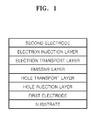
- FIG. 1 is a schematic illustrating an organic light emitting diode according to an embodiment of the present invention
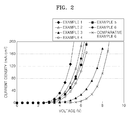
- FIG. 2 is a graph comparing voltage-current density properties of the organic light emitting diodes prepared according to Examples 2 through 6 and the organic light emitting diode prepared according to the Comparative Example;
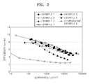
- FIG. 3 is a graph comparing luminance-efficiency properties of the organic light emitting diodes prepared according to Examples 2 through 6 and the organic light emitting diode prepared according to the Comparative Example.
- Subject-matter of the invention is an imidazopyridine-based compound according to an embodiment of the present invention which is represented by Formula 1 below.
- L 1 or L 2 bind an imidazopyridine ring to at least one of the 1 st through 8 th positions of an anthracene ring, but not to the 9 th or 10 th position of the ring.
- the imidazopyridine ring is not bound to the 9 th or 10 th position of the anthracene ring because the 9 th and 10 th positions are structurally weak points.
- the group can be easily decomposed from the anthracene ring by heat, oxygen, moisture or the like.
- an imidazopyridine ring which is electron deficient
- the imidazopyridine ring can be easily decomposed from the anthracene ring by heat generated during formation of the organic layer (for example, by deposition or the like) of an organic light emitting diode (OLED).
- the imidazopyridine ring can also be decomposed from the anthracene ring during operation of the organic light emitting diode, thus deteriorating the characteristics of the organic light emitting diode.
- an aromatic ring such as an aryl group or a heteroaryl group is bound to the 9 th or 10 th position of the anthracene ring.
- an imidazopyridine ring (which is electron deficient) is bound to at least one of the 1 st through 8 th positions of the anthracene ring, preferably over L 1 or L 2 . Accordingly, the imidazopyridine-based compound shows improved structural stability and electron mobility.
- R 1 , R 2 , R 3 , R 4 , R 5 , R 6 , R 7 , R 8 , R 9 , R 10 , R 11 and R 12 are each independently selected from hydrogen atoms, halogen atoms, hydroxyl groups, cyano groups, substituted or unsubstituted C 1 -C 30 alkyl groups, substituted or unsubstituted C 1 -C 3o alkoxy groups, substituted or unsubstituted C 1 -C 30 acyl groups, substituted or unsubstituted C 2 -C 30 alkenyl groups, substituted or unsubstituted C 2 -C 30 alkynyl groups, substituted or unsubstituted C 6 -C 30 aryl groups, and substituted or unsubstituted C 3 -C 30 heteroaryl groups.
- R 4 , R 5 , R 6 and R 7 may be bound to each other to form a saturated or unsaturated ring, and/or at least two of adjoining R 9 , R 10 , R 11 and R 12 may be bound to each other to form a saturated or unsaturated ring.
- x and y are independently of each other 0, 1,2,3 or 4.
- R 1 through R 12 may each be independently selected from hydrogen atoms, substituted or unsubstituted C 1 -C 10 alkyl groups, substituted or unsubstituted C 2 -C 10 alkenyl groups, substituted or unsubstituted C 6 -C 12 aryl groups, and substituted or unsubstituted C 3 -C 12 heteroaryl groups.
- At least two of R 4 , R 5 , R 6 and R 7 , or at least two of Rg, R 10 , R 11 and R 12 are bound to one another to form a substituted or unsubstituted C 6 -C 12 aromatic ring.
- L 1 and L 2 may each be independently selected from single bonds, substituted or unsubstituted C 1 -C 30 alkylene groups, substituted or unsubstituted C 6 -C 30 arylene groups, and substituted or unsubstituted C 3 -C 30 heteroarylene groups.
- L 1 and L 2 may each be independently selected from substituted or unsubstituted C 6 -C 12 arylene groups, and substituted or unsubstituted C 3 -C 12 heteroarylene groups.
- L 1 and/or L 2 are preferably a phenylene group.
- Ar 1 and Ar 2 may each be independently selected from substituted or unsubstituted C 6 -C 30 aryl groups, and substituted or unsubstituted C 3 -C 30 heteroaryl groups.
- Ar 1 and Ar 2 may each be independently selected from substituted or unsubstituted C 6 -C l2 aryl groups, and substituted or unsubstituted C 3 -C 12 heteroaryl groups.
- Ar 1 and Ar 2 are identical and selected from substituted or unsubstituted C 6 -C 12 aryl groups, especially preferable is an unsubstituted phenyl or naphthyl group.
- p and q are each independently selected from integers ranging from 1 to 5. In one embodiment, for example, p and q are each integers ranging from 1 to 3. That is, at least one imidazopyridine ring can be bound to L 1 or L 2 , which can be determined by the chemical structure of L 1 or L 2 .
- m and n are each independently selected from integers ranging from 0 to 4, but both m and n are not 0. That is, in an imidazopyridine-based compound according to one embodiment of the present invention, at least one of the 1 st through 8 th positions of the anthracene ring is bound to an imidazopyridine ring, preferably over L 1 and L 2 respectively.
- m and n can be 0 and 1.
- m may be 0, and n may be 1.
- both m and n may be 1.
- Nonlimiting examples of suitable unsubstituted C 1 -C 30 alkyl groups for use in the compounds represented by Formula 1 include methyl groups, ethyl groups, propyl groups, isobutyl groups, sec-butyl groups, pentyl groups, iso-amyl groups, hexyl groups, and the like.
- At least one hydrogen atom of the alkyl group may be substituted with a substituent selected from halogen atoms, hydroxyl groups, nitro groups, cyano groups, amino groups, amidino groups, hydrazine, hydrazone, carboxyl groups or salts thereof, sulfonic acid groups or salts thereof, phosphoric acid groups or salts thereof, C 1 -C 30 alkyl groups, C 1 -C 30 alkenyl groups, C 1 -C 30 alkynyl groups, C 6 -C 30 aryl groups, C 7 -C 20 arylalkyl groups, C 2 -C 20 heteroaryl groups and C 3 -C 30 heteroarylalkyl groups.
- a substituent selected from halogen atoms, hydroxyl groups, nitro groups, cyano groups, amino groups, amidino groups, hydrazine, hydrazone, carboxyl groups or salts thereof, sulfonic acid groups or salts thereof, phosphoric acid groups
- Nonlimiting examples of suitable unsubstituted C 1 -C 30 alkoxy groups for use in compounds represented by Formula 1 include methoxy groups, ethoxy groups, phenyloxy groups, cyclohexyloxy groups, naphthyloxy groups, isopropyloxy groups, diphenyloxy groups and the like. At least one hydrogen atom of the alkoxy group can be substituted with a substituent selected from those discussed above with respect to the C 1 -C 30 alkyl groups.
- Nonlimiting examples of suitable unsubstituted C 1 -C 30 acyl groups for use in compounds represented by Formula 1 include acetyl groups, ethylcarbonyl groups, isopropylcarbonyl groups, phenylcarbonyl groups, naphthylenecarbonyl groups, diphenylcarbonyl groups, cyclohexylcarbonyl groups, and the like. At least one hydrogen atom of the C 1 -C 30 acyl group can be substituted with a substituent selected from those discussed above with respect to the C 1 -C 30 alkyl groups.
- Nonlimiting examples of suitable unsubstituted C 2 -C 30 alkenyl groups for use in the compounds represented by Formula 1 include compounds containing a carbon-carbon double bond in the middle or end of an alkyl group defined above.
- the unsubstituted C 2 -C 30 alkenyl group may be selected from ethylene groups, propylene groups, butylene groups, hexylene groups, and the like.
- At least one hydrogen atom of the alkenyl group can be substituted with a substituent selected from those discussed above with respect to the C 1 -C 30 alkyl groups.
- Nonlimiting examples of suitable unsubstituted C 2 -C 30 alkynyl groups for use in compounds represented by Formula 1 include compounds containing a carbon-carbon triple bond in the middle or end of an alkyl group defined above.
- the unsubstituted C 2 -C 30 alkynyl group may be selected from acetylene groups, propylene groups, phenylacetylene groups, naphthylacetylene groups, isopropylacetylene groups, t-butylacetylene groups, diphenylacetylene groups, and the like.
- At least one hydrogen atom of the alkynyl group can be substituted with a substituent selected from those discussed above with respect to the C 1 -C 30 alkyl groups.
- Nonlimiting examples of suitable unsubstituted C 6 -C 30 aryl groups for use in compounds represented by Formula 1 include C 6 -C 30 carbocyclic aromatic systems containing at least one aromatic ring.
- the at least one aromatic ring can include at least two rings fused with each other, or bound to each other by a single bond, or the like.
- At least one hydrogen atom of the aryl group can be substituted with a substituent selected from those discussed above with respect to the C 1 -C 30 alkyl groups.
- the substituted or unsubstituted C 6 -C 30 aryl group can be selected from phenyl groups, C 1 -C 10 alkylphenyl groups (for example, an ethylphenyl group), C 1 -C 10 alkylbiphenyl groups (for example, an ethylbiphenyl group), halophenyl groups (for example, o-, m- and p-fluorophenyl groups, and dichlorophenyl groups), dicyanophenyl groups, trifluoro methoxy phenyl groups, o-, m-, and p-tolyl groups, o-, m- and p-cumenyl groups, mesityl groups, phenoxy phenyl groups, ( ⁇ , ⁇ -dimethylbenzyl)phenyl groups, (N,N'-dimethyl)aminophenyl groups, (N,N'-diphenyl)aminophenyl groups, pen
- Nonlimiting examples of suitable unsubstituted C 3 -C 30 heteroaryl groups for use in compounds represented by Formula 1 include systems having at least one aromatic ring that includes at least one hetero atom selected from N, O, P and S, where the remaining ring member is carbon.
- the at least one aromatic ring can be at least two rings that are fused with each other, or bound to each other by a single bond, or the like.
- At least one hydrogen atom of the heteroaryl group can be substituted with a substituent selected from those discussed above with respect to the C 1 -C 30 alkyl groups.
- Nonlimiting examples of suitable unsubstituted C 3 -C 30 heteroaryl groups for use in compounds represented by Formula 1 include pyrazolyl groups, imidazolyl groups, oxazolyl groups, thiazolyl groups, triazolyl groups, tetrazolyl groups, oxadiazolyl groups, pyridinyl groups, pyridazinyl groups, pyrimidinyl groups, triazinyl groups, carbazolyl groups, indolyl groups, quinolinyl groups, isoquinolinyl groups, and the like.
- Nonlimiting examples of suitable substituents for R 1 through R 12 of Formula 1 include hydrogen atoms, C 1 -C 10 alkyl groups, C 1 -C 10 haloalkyl groups, C 2 -C 10 alkenyl groups, C 2 -C 10 haloalkenyl groups, phenyl groups, halophenyl groups, C 1 -C 10 alkylphenyl groups, C 1 -C 10 alkoxyphenyl groups, naphthyl groups, halonaphthyl groups, C 1 -C 10 alkylnaphthyl groups, and C 1 -C 10 alkoxynaphthyl groups.
- Nonlimiting examples of suitable substituents for L 1 and L 2 of Formula 1 include phenylene groups, halophenylene groups, C 1 -C 10 alkylphenylene groups, C 1 -C 10 alkoxyphenylene groups, naphthylene groups, halonaphthylene groups, C 1 -C 10 alkylnaphthylene groups, and C 1 -C 10 alkoxynaphthylene groups.
- Nonlimiting examples of suitable substituents for Ar 1 and Ar 2 of Formula 1 include phenyl groups, halophenyl groups, C 1 -C 10 alkylphenyl groups, C 1 -C 10 alkoxyphenyl groups, naphthyl groups, halonaphthyl groups, C 1 -C 10 alkylnaphthyl groups, C 1 -C 10 alkoxynaphthyl groups, pyridinyl groups, halopyridinyl groups, C 1 -C 10 alkylpyridinyl groups, C 1 -C 10 alkoxypyridinyl groups, quinolinyl groups, haloquinolinyl groups, C 1 -C 10 alkylquinolinyl groups, C 1 -C 10 alkoxyquinolinyl groups, isoquinolinyl groups, haloisoquinolinyl groups, C 1 -C 10 alkylisoquinolinyl groups, and C 1 -
- the imidazopyridine-based compound may be represented by one of Formulae 1a, 1b, 1c and 1d.
- R 3 through R 12 , Ar 1 and Ar 2 are the same as described above with respect to Formula 1.
- R 3 and R 8 is independently selected from the group consisting of hydrogen atoms, C 1 -C 10 alkyl groups, preferably methyl, ethyl, propyl, butyl, pentyl, and/or C 6 -C l2 aryl groups
- R 4 , R 5 , R 6 and R 7 is a hydrogen atom and/or at least two of R 4 , R 5 , R 6 and R 7 form a phenyl ring
- R 9 , R 10 , R 11 and R 12 is a hydrogen atom and/or at least two of R 9 , R 10 , R 11 and R 12 form a phenyl ring
- Ar 1 and Ar 2 are identical and selected from the group consisting of C 6 -C 12 aryl groups.
- Nonlimiting examples of suitable compounds for use as the imidazopyridine-based compound represented by Formula 1 include Compounds 1 through 11 below.
- the imidazopyridine-based compound represented by Formula 1 can be prepared using various methods.
- the imidazopyridine-based compound represented by Formula 1 can be obtained by reacting a compound represented by Formula 2 below with at least one of a compound represented by Formula 3 and a compound represented by Formula 4, both shown below.
- R 1 through R 12 , L 1 , L 2 , Ar 1 , Ar 2 , p, q, n and m, x and y are the same as defined above.
- the imidazopyridine-based compound represented by Formula 1 can be prepared by a Suzuki reaction method.
- an imidazopyridine-based compound represented by Formula 1 can be used to form an organic layer preferably for use of an organic light emitting diode.
- an organic light emitting diode includes a first electrode, a second electrode, and an organic layer including an imidazopyridine-based compound represented by Formula 1 between the first and second electrodes.
- the organic layer may be an electron transport layer.
- the organic light emitting diode may further include a layer selected from a hole injection layer, a hole transport layer, an electron blocking layer, an emissive layer, a hole blocking layer, an electron transport layer, an electron injection layer, and combinations thereof.
- the organic light emitting diode may further include a hole injection layer, a hole transport layer, an emissive layer and an electron injection layer.
- the organic light emitting diode may further include a hole blocking layer.
- the organic light emitting diode may have various other structures.
- FIG. 1 illustrates a structure of the organic light emitting diode according to one embodiment of the present invention.
- the organic light emitting diode illustrated in FIG. 1 has a first electrode/hole injection layer/hole transport layer/emissive layer/electron transport layer/electron injection layer/second electrode structure.
- the organic light emitting diode is not limited to this structure and may have various other structures, such as a first electrode/hole injection layer/emissive layer/electron transport layer/electron injection layer/second electrode structure, or a first electrode/hole injection layer/hole transport layer/emissive layer/hole blocking layer/electron transport layer/electron injection layer/second electrode structure.
- the electron transport layer can be formed of an imidazopyridine-based compound represented by Formula 1.
- the emissive layer of the organic light emitting diode may include a red, green, blue or white phosphorescent or fluorescent dopant.
- the phosphorescent dopant may be an organic metal compound which contains a metal selected from lr, Pt, Os, Ti, Zr, Hf, Eu, Tb, Tm, and combinations thereof.
- a first electrode is formed by depositing or sputtering a high work-function material on a substrate.
- the first electrode can be an anode or a cathode.
- the substrate which can be any substrate used in conventional organic light emitting devices, may be a glass substrate or a transparent plastic substrate that can be easily treated, is waterproof, and has excellent mechanical strength, thermal stability, transparency, and surface smoothness.
- the first electrode can be formed of ITO, IZO, SnO 2 , ZnO, or any transparent material that has high conductivity.
- a hole injection layer can be formed on the first electrode by vacuum deposition, spin coating, casting, Langmuir Blodgett (LB) deposition, or the like.
- the vacuum deposition conditions may vary depending on the compound used to form the HIL, and the desired structure and thermal properties of the HIL to be formed. In general, however, vacuum deposition may be performed at a deposition temperature ranging from about 100°C to about 500°C, a pressure ranging from about 10 -8 to about 10 -3 torr, a deposition speed ranging from about 0.01 to about 100 ⁇ /sec.
- the thickness of the vacuum deposited layer may range from about 10 ⁇ to about 5 ⁇ m.
- coating conditions may vary depending on the compound used to form the HIL, and the desired structure and thermal properties of the HIL to be formed. In general, however, the coating speed may range from about 2,000 to about 5,000 rpm, and the temperature for heat treatment (which is performed to remove solvent after coating) may range from about 80 to about 200°C.
- the HIL material is not particularly limited and can be any known material used to form HILs.
- suitable HIL materials include phthalocyanine compounds (such as copperphthalocyanine), star-burst type amine derivatives (such as TCTA (shown below), m-MTDATA (shown below), and m-MTDAPB), soluble and conductive polymers (such as polyaniline/Dodecylbenzenesulfonic acid (Pani/DBSA), poly(3,4-ethylenedioxythiophene)/poly(4-styrenesulfonate) (PEDOT/PSS), polyaniline/camphor sulfonic acid (Pani/CSA), (polyaniline)/poly(4-styrenesulfonate) (PANI/PSS)), and the like.
- phthalocyanine compounds such as copperphthalocyanine
- star-burst type amine derivatives such as TCTA (shown below), m-MTDATA (shown below), and
- the thickness of the HIL may range from about 100 to about 10,000 ⁇ . In one embodiment, for example, the thickness may range from about 100 to about 1,000 ⁇ . When the thickness of the HIL is within the above described ranges, the HIL has excellent hole injecting abilities, and organic light emitting diodes having excellent driving voltages can be obtained.
- a hole transport layer can be formed on the HIL by vacuum deposition, spin coating, casting, LB deposition, or the like.
- the conditions for deposition and coating are similar to those for the formation of the HIL, although the deposition or coating conditions may vary according to the material used to form the HTL.
- the HTL material is not particularly limited and can be any known material for use as a HTL.
- suitable HTL materials include carbazole derivatives (such as N-phenylcarbazole and polyvinylcarbazole), typical amine derivatives having aromatic condensation rings (such as N,N'-bis(3-methylphenyl)-N,N'-diphenyl-[1,1-biphenyl]-4,4'-diamine (TPD shown below), and N,N'-di(naphthalene-1-yl)-N,N'-diphenyl benzydine ( ⁇ -NPD shown below)), and the like.
- carbazole derivatives such as N-phenylcarbazole and polyvinylcarbazole
- typical amine derivatives having aromatic condensation rings such as N,N'-bis(3-methylphenyl)-N,N'-diphenyl-[1,1-biphenyl]-4,4'-diamine (TPD shown below), and
- the thickness of the HTL may range from about 50 to about 1,000 ⁇ . ln one embodiment, for example, the thickness ranges from about 100 to about 600 ⁇ . When the thickness of the HTL is within the above described ranges, the HTL has excellent hole transporting abilities, and organic light emitting diodes having excellent driving voltages can be obtained.
- An emissive layer can be formed on the HTL by vacuum deposition, spin coating, casting, LB deposition, or the like.
- EML emissive layer
- the conditions for deposition and coating are similar to those for the formation of the HIL, although the deposition and coating conditions may vary according to the material used to form the EML.
- the emissive layer can be formed of various known emissive materials, and can include known hosts and dopants.
- the dopant can be a known fluorescent dopant or a known phosphorescent dopant.
- suitable host materials include Alq 3 , 4,4'-N,N'-dicarbazole-biphenyl (CBP), poly(n-vinylcarbazole) (PVK), distyrylarylene (DSA), and the like.
- Nonlimiting examples of suitable fluorescent dopants include IDE102 and IDE105 obtained from Idemitsu Co.
- suitable phosphorescent dopants include green phosphorescent dopants (such as Ir(ppy) 3 (ppy is an abbreviation of phenylpyridine), (4,6-F2ppy) 2 Irpic, TEB002 obtained from Covion, Ltd.), red phosphorescent dopants (such as platinum(II) octaethylporphyrin (PtOEP)), compounds represented by Formula 5 below, Firpric, TBPe, and the like.
- the dopant may be present in an amount ranging from about 0.1 to about 20 parts by weight based on 100 parts by weight of the total weight of the emissive layer (that is, the total weight of the host and dopant). In one embodiment, the dopant is present in an amount ranging from about 0.5 to about 12 parts by weight. When the dopant is present in an amount greater than about 0.1 parts by weight, the effect of the addition of the dopant increases. Also, when the amount of either the phosphorescent or fluorescent dopant is less than about 20 parts by weight, concentration quenching can be substantially prevented.
- the thickness of the EML may range from about 100 to about 1,000 ⁇ . In one embodiment, for example, the thickness ranges from about 200 to about 600 ⁇ . When the thickness of the EML is within these ranges, the EML has excellent emissive abilities, and organic light emitting diodes having excellent driving voltages can be obtained.
- HBL hole blocking layer
- EML electron transport layer
- the HBL material is not particularly limited and can be any known material used to form HBLs.
- suitable HBL materials include oxadiazole derivatives, triazole derivatives, phenanthroline derivatives, Balq, BCP, and the like.
- the thickness of the HBL may range from about 50 to about 1,000 ⁇ . In one embodiment, for example, the thickness ranges from about 100 to about 300 ⁇ . When the thickness of the HBL is within these ranges, the HBL has excellent hole blocking abilities, and organic light emitting devices having excellent driving voltages can be obtained.
- An electron transport layer may be formed on the HBL by vacuum deposition, spin coating, casting, or the like.
- the conditions for deposition and coating are, in general, similar to those for the formation of the HIL, although the deposition and coating conditions may vary according to the material used to form the ETL.
- the ETL may be formed of an imidazopyridine-based compound represented by Formula 1.
- the ETL may also be formed of a quinoline derivative, for example, tris(8-quinolinorate)aluminum (Alq 3 ), TAZ, or the like, which are known in the art.
- the thickness of the ETL may range from about 100 to about 1,000 ⁇ . In one embodiment, for example, the thickness ranges from about 100 to about 500 ⁇ . When the thickness of the ETL is within these ranges, the ETL has excellent electron transporting abilities, and organic light emitting diodes having excellent driving voltages can be obtained.
- an electron injection layer may be deposited on the ETL.
- the EIL makes it easy for electrons to be injected from a cathode.
- the EIL may be formed of LiF, NaCl, CsF, Li 2 O, BaO, or the like, which materials are known in the art.
- Deposition and coating conditions for formation of the EIL are, in general, similar to the conditions for the formation of the HIL, although they may vary according to the material used to form the EIL.
- the thickness of the EIL may range from about 1 to about 100 ⁇ . ln one embodiment, for example, the thickness ranges from about 5 to about 90 ⁇ . When the thickness of the EIL is within these ranges, the EIL has excellent electron injecting abilities, and organic light emitting diodes having excellent driving voltages can be obtained.
- a second electrode can be formed on the EIL by vacuum deposition, sputtering, or the like.
- the second electrode can be used as a cathode or an anode.
- the second electrode may be formed of a low work-function metal, an alloy, an electrically conductive compound, or a combination thereof.
- suitable materials for the second electrode include Li, Mg, Al, Al-Li, Ca, Mg-In, Mg-Ag, and the like.
- a transparent cathode formed of ITO or IZO can be used to produce a front surface light emitting diode.
- Compound 3 was prepared in the same manner as in Synthesis Example 1, except that Intermediate 3d was used instead of intermediate 1d. Intermediate 3d was obtained using 2,4'-dibromopropiophenone instead of 2,4'-dibromoacetophenone. 5 g of Intermediate 1c (10.54 mmol) and 2.75 g of Intermediate 3d (9.58 mmol) were subjected to a Suzuki reaction, yielding 4.15 g of Compound 3 in the form of a pale yellow powder (yield 68%).
- Compound 2 was prepared in the same manner as in Synthesis Example 1, except that Intermediate 2c was used instead of Intermediates 1b and 1c. Intermediate 2c was obtained using phenylmagnesiumbromide instead of 2-naphthylmagnesiumbromide. 5 g of Intermediate 2c (13.36 mmol) and 3.32 g of Intermediate 1d (12.15 mmol) were subjected to a Suzuki reaction, yielding 4.64 g of Compound 2 in the form of pale yellow powder (yield 73%).
- ITO glass substrate was cut to a size of 50 mm x 50 mm x 0.7 mm, ultrasonically washed with isopropyl alcohol for five minutes and with pure water for 5 minutes. The substrate was then washed with UV ozone for 30 minutes.
- m-MTDATA was vacuum deposited on the substrate to form a hole injection layer with a thickness of 750 ⁇ .
- ⁇ -NPD was then vacuum deposited on the hole injection layer to form a hole transport layer with a thickness of 150 ⁇ .
- An emissive layer with a thickness of 300 ⁇ was formed on the hole transport layer using 97wt% of DSA as a host, and 3 wt% of TBPe as a dopant.
- Compound 1 prepared by Synthesis Example 1 was vacuum deposited on the emissive layer to form an electron transport layer with a thickness of 200 ⁇ .
- LiF was vacuum deposited on the electron transport layer to form an electron injection layer with a thickness of 80 ⁇ , and then Al was vacuum deposited on the electron injection layer to form a cathode with a thickness of 3000 ⁇ to complete an organic light emitting diode.
- An organic light emitting diode was manufactured as in Example 1, except that Compound 4 prepared in Synthesis Example 2 was used as the material of the electron transport layer.
- An organic light emitting diode was manufactured as in Example 1, except that Compound 7 prepared in Synthesis Example 3 was used as the material of the electron transport layer.
- An organic light emitting diode was manufactured as in Example 1, except that Compound 3 prepared in Synthesis Example 4 was used as the material of the electron transport layer.
- An organic light emitting diode was manufactured as in Example 1, except that Compound 2 prepared in Synthesis Example 5 was used as the material of the electron transport layer.
- An organic light emitting diode was manufactured as in Example 1, except that Compound 11 prepared in Synthesis Example 6 was used as the material of the electron transport layer.
- An organic light emitting diode was manufactured as in Example 1, except that Alq 3 (8-hydroxyquinoline aluminum complex) was used as the material of the electron transport layer.
- FIG. 2 is a graph comparing the voltage-current density properties of the organic light emitting diode of Examples 1 through 6 and the organic light emitting diode of the Comparative Example.
- FIG. 2 is a graph comparing the luminance-efficiency properties of the organic light emitting diode of Examples 1 through 6 and the organic light emitting diode of the Comparative Example.
- an organic light emitting diode including an organic layer formed of an imidazopyridine-based compound represented by Formula 1 has higher luminance, higher efficiency, lower driving voltage and a longer life-time than a conventional organic light emitting diode.
- the imidazopyridine-based compounds represented by Formula 1 have high electron transporting abilities, and organic light emitting diodes including organic layers having the imidazopyridine-based compounds represented by Formula 1 have low driving voltages, high luminance, high efficiencies and long life-times.
Abstract
Description
- The invention refers to new imidazopyridine-based compounds of Formula 1 and their use in an organic layer, preferably as an electron transport layer of an organic light emitting diode (OLED). Furthermore the invention refers to an OLED comprising at least an imidazopyridine-based compound of
Formula 1. - The present invention relates to imidazopyridine-based compounds and to organic light emitting diodes including organic layers comprising the imidazopyridine-based compounds. More particularly, the invention is directed to imidazopyridine-based compounds suitable for electron transport layers of organic light emitting diodes and to organic light emitting diodes including organic layers comprising the imidazopyridine-based compounds.
- Organic Light emitting diodes (OLEDs) are self-emitting diodes having wide viewing angles, excellent contrast, and quick response times.
- Further, organic light emitting diodes have good luminance, operating voltage and response times, and can realize multicolor images.
- In a conventional organic light emitting diode, an anode is formed on a substrate, and a hole transport layer, an emissive layer, an electron transport layer and a cathode are sequentially formed on the anode. The hole transport layer, the emissive layer and the electron transport layer are organic thin films formed of organic compounds. An organic light emitting diode having such a structure operates as follows. When a voltage is applied to the anode and cathode, holes injected from the anode migrate to the emissive layer via the hole transport layer. The electrons injected from the cathode migrate to the emissive layer via the electron transport layer. The holes and the electrons recombine with each other in the emissive layer to generate excitons. When the excitons drop from an excited state to a ground state, fluorescent molecules of the emissive layer emit light. Heteroaromatic compounds such as oxadiazoles, thiadiazoles, pyrimidines and the like may be used as the material for forming the electron transport layer. However, conventional organic light emitting diodes do not have satisfactory driving voltages, luminance, current densities, power efficiencies, life-times and the like.
- It is an object of the invention to find materials able as an organic layer in an OLED, especially materials for forming an electron transport layer which improves the above properties.
- According to one embodiment of the present invention, imidazopyridine-based compounds of Formula 1 are provided which have high electron transport capabilities.
- In another embodiment of the present invention, an organic light emitting diode using such a imidazopyridine-based compound of Formula 1 has high efficiency, low driving voltage, high luminance and a long life-time.
According to an embodiment of the present invention, the new imidazopyridine-based compounds are represented by Formula 1 below.
Formula 1, p and q are each independently selected from integers ranging from 1 to 5, m and n are each independently selected from integers ranging from 0 to 4, and both m and n are not 0. R1, R2, R3, R4, R5, R6, R7, R8, R9, R10, R11 and R12 are each independently selected from hydrogen atoms, halogen atoms, hydroxyl groups, cyano groups, substituted or unsubstituted C1-C30 alkyl groups, substituted or unsubstituted C1-C30 alkoxy groups, substituted or unsubstituted C1-C30 acyl groups, substituted or unsubstituted C2-C30 alkenyl groups, substituted or unsubstituted C2-C30 alkynyl groups, substituted or unsubstituted C6-C30 aryl groups, and substituted or unsubstituted C3-C30 heteroaryl groups. At least two of R4, R5, R6 and R7 are bound to each other to form a saturated or unsaturated ring. At least two of R9, R10, R11 and R12 are bound to each other to form a saturated or unsaturated ring. L1 and L2 may each be independently selected from single bonds, substituted or unsubstituted C1-C30 alkylene groups, substituted or unsubstituted C6-C30 arylene groups, and substituted or unsubstituted C3-C30 heteroarylene groups. Ar1 and Ar2 may each be independently selected from substituted or unsubstituted C6-C30 aryl groups, and substituted or unsubstituted C3-C30 heteroaryl groups. x and y are independently of each other 0, 1, 2, 3 or 4. - According to another embodiment of the present invention, an organic light emitting diode (OLED) comprises a first electrode, a second electrode, and an organic layer between the first second electrodes, the organic layer including a imidazopyridine-based compound of Formula 1.
- The imidazopyridine-based compounds represented by Formula 1 have high electron transporting abilities, enabling organic light emitting diodes including organic layers having an imidazopyridine-based compound to have low driving voltages, high current densities, high luminance, high efficiencies and long life-times.
- The above and other features and advantages of the present invention will become more apparent by reference to the following detailed description when considered in conjunction with the attached drawings in which:
- FIG. 1 is a schematic illustrating an organic light emitting diode according to an embodiment of the present invention;
- FIG. 2 is a graph comparing voltage-current density properties of the organic light emitting diodes prepared according to Examples 2 through 6 and the organic light emitting diode prepared according to the Comparative Example; and
- FIG. 3 is a graph comparing luminance-efficiency properties of the organic light emitting diodes prepared according to Examples 2 through 6 and the organic light emitting diode prepared according to the Comparative Example.
- Subject-matter of the invention is an imidazopyridine-based compound according to an embodiment of the present invention which is represented by Formula 1 below.

Formula 1, L1 or L2 bind an imidazopyridine ring to at least one of the 1st through 8th positions of an anthracene ring, but not to the 9th or 10th position of the ring. The imidazopyridine ring is not bound to the 9th or 10th position of the anthracene ring because the 9th and 10th positions are structurally weak points. Thus, when the 9th and 10th positions of the anthracene ring are substituted with a group having a specific function, the group can be easily decomposed from the anthracene ring by heat, oxygen, moisture or the like. For example, when an imidazopyridine ring (which is electron deficient) is bound to the 9th or 10th position of the anthracene ring, the imidazopyridine ring can be easily decomposed from the anthracene ring by heat generated during formation of the organic layer (for example, by deposition or the like) of an organic light emitting diode (OLED). The imidazopyridine ring can also be decomposed from the anthracene ring during operation of the organic light emitting diode, thus deteriorating the characteristics of the organic light emitting diode. However, in the imidazopyridine-based compound according to one embodiment of the present invention, an aromatic ring such as an aryl group or a heteroaryl group is bound to the 9th or 10th position of the anthracene ring. In addition, an imidazopyridine ring (which is electron deficient) is bound to at least one of the 1st through 8th positions of the anthracene ring, preferably over L1 or L2. Accordingly, the imidazopyridine-based compound shows improved structural stability and electron mobility. - In
Formula 1, R1, R2, R3, R4, R5, R6, R7, R8, R9, R10, R11 and R12 are each independently selected from hydrogen atoms, halogen atoms, hydroxyl groups, cyano groups, substituted or unsubstituted C1-C30 alkyl groups, substituted or unsubstituted C1-C3o alkoxy groups, substituted or unsubstituted C1-C30 acyl groups, substituted or unsubstituted C2-C30 alkenyl groups, substituted or unsubstituted C2-C30 alkynyl groups, substituted or unsubstituted C6-C30 aryl groups, and substituted or unsubstituted C3-C30 heteroaryl groups. Furthermore at least two of adjoining R4, R5, R6 and R7 may be bound to each other to form a saturated or unsaturated ring, and/or at least two of adjoining R9, R10, R11 and R12 may be bound to each other to form a saturated or unsaturated ring.
x and y are independently of each other 0, 1,2,3 or 4. - In one embodiment, R1 through R12 may each be independently selected from hydrogen atoms, substituted or unsubstituted C1-C10 alkyl groups, substituted or unsubstituted C2-C10 alkenyl groups, substituted or unsubstituted C6-C12 aryl groups, and substituted or unsubstituted C3-C12 heteroaryl groups.
- According to another embodiment, at least two of R4, R5, R6 and R7, or at least two of Rg, R10, R11 and R12, are bound to one another to form a substituted or unsubstituted C6-C12 aromatic ring.
- In
Formula 1, L1 and L2 may each be independently selected from single bonds, substituted or unsubstituted C1-C30 alkylene groups, substituted or unsubstituted C6-C30 arylene groups, and substituted or unsubstituted C3-C30 heteroarylene groups. In one embodiment, for example, L1 and L2 may each be independently selected from substituted or unsubstituted C6-C12 arylene groups, and substituted or unsubstituted C3-C12 heteroarylene groups.
L1 and/or L2 are preferably a phenylene group. - In
Formula 1, Ar1 and Ar2 may each be independently selected from substituted or unsubstituted C6-C30 aryl groups, and substituted or unsubstituted C3-C30 heteroaryl groups. In one embodiment, for example, Ar1 and Ar2 may each be independently selected from substituted or unsubstituted C6-Cl2 aryl groups, and substituted or unsubstituted C3-C12 heteroaryl groups.
Preferably Ar1 and Ar2 are identical and selected from substituted or unsubstituted C6-C12 aryl groups, especially preferable is an unsubstituted phenyl or naphthyl group. - In Formula 1, p and q are each independently selected from integers ranging from 1 to 5. In one embodiment, for example, p and q are each integers ranging from 1 to 3. That is, at least one imidazopyridine ring can be bound to L1 or L2, which can be determined by the chemical structure of L1 or L2.
- In Formula 1, m and n are each independently selected from integers ranging from 0 to 4, but both m and n are not 0. That is, in an imidazopyridine-based compound according to one embodiment of the present invention, at least one of the 1st through 8th positions of the anthracene ring is bound to an imidazopyridine ring, preferably over L1 and L2 respectively. In one embodiment, for example, m and n can be 0 and 1. Preferably m may be 0, and n may be 1. In another embodiment, both m and n may be 1.
- Nonlimiting examples of suitable unsubstituted C1-C30 alkyl groups for use in the compounds represented by
Formula 1 include methyl groups, ethyl groups, propyl groups, isobutyl groups, sec-butyl groups, pentyl groups, iso-amyl groups, hexyl groups, and the like. At least one hydrogen atom of the alkyl group may be substituted with a substituent selected from halogen atoms, hydroxyl groups, nitro groups, cyano groups, amino groups, amidino groups, hydrazine, hydrazone, carboxyl groups or salts thereof, sulfonic acid groups or salts thereof, phosphoric acid groups or salts thereof, C1-C30 alkyl groups, C1-C30 alkenyl groups, C1-C30 alkynyl groups, C6-C30 aryl groups, C7-C20 arylalkyl groups, C2-C20 heteroaryl groups and C3-C30 heteroarylalkyl groups. - Nonlimiting examples of suitable unsubstituted C1-C30 alkoxy groups for use in compounds represented by
Formula 1 include methoxy groups, ethoxy groups, phenyloxy groups, cyclohexyloxy groups, naphthyloxy groups, isopropyloxy groups, diphenyloxy groups and the like. At least one hydrogen atom of the alkoxy group can be substituted with a substituent selected from those discussed above with respect to the C1-C30 alkyl groups. - Nonlimiting examples of suitable unsubstituted C1-C30 acyl groups for use in compounds represented by
Formula 1 include acetyl groups, ethylcarbonyl groups, isopropylcarbonyl groups, phenylcarbonyl groups, naphthylenecarbonyl groups, diphenylcarbonyl groups, cyclohexylcarbonyl groups, and the like. At least one hydrogen atom of the C1-C30 acyl group can be substituted with a substituent selected from those discussed above with respect to the C1-C30 alkyl groups. - Nonlimiting examples of suitable unsubstituted C2-C30 alkenyl groups for use in the compounds represented by
Formula 1 include compounds containing a carbon-carbon double bond in the middle or end of an alkyl group defined above. For example, the unsubstituted C2-C30 alkenyl group may be selected from ethylene groups, propylene groups, butylene groups, hexylene groups, and the like. At least one hydrogen atom of the alkenyl group can be substituted with a substituent selected from those discussed above with respect to the C1-C30 alkyl groups. - Nonlimiting examples of suitable unsubstituted C2-C30 alkynyl groups for use in compounds represented by
Formula 1 include compounds containing a carbon-carbon triple bond in the middle or end of an alkyl group defined above. For example, the unsubstituted C2-C30 alkynyl group may be selected from acetylene groups, propylene groups, phenylacetylene groups, naphthylacetylene groups, isopropylacetylene groups, t-butylacetylene groups, diphenylacetylene groups, and the like. At least one hydrogen atom of the alkynyl group can be substituted with a substituent selected from those discussed above with respect to the C1-C30 alkyl groups. - Nonlimiting examples of suitable unsubstituted C6-C30 aryl groups for use in compounds represented by
Formula 1 include C6-C30 carbocyclic aromatic systems containing at least one aromatic ring. The at least one aromatic ring can include at least two rings fused with each other, or bound to each other by a single bond, or the like. At least one hydrogen atom of the aryl group can be substituted with a substituent selected from those discussed above with respect to the C1-C30 alkyl groups. - The substituted or unsubstituted C6-C30 aryl group can be selected from phenyl groups, C1-C10 alkylphenyl groups (for example, an ethylphenyl group), C1-C10 alkylbiphenyl groups (for example, an ethylbiphenyl group), halophenyl groups (for example, o-, m- and p-fluorophenyl groups, and dichlorophenyl groups), dicyanophenyl groups, trifluoro methoxy phenyl groups, o-, m-, and p-tolyl groups, o-, m- and p-cumenyl groups, mesityl groups, phenoxy phenyl groups, (α,α-dimethylbenzyl)phenyl groups, (N,N'-dimethyl)aminophenyl groups, (N,N'-diphenyl)aminophenyl groups, pentalenyl groups, indenyl groups, naphthyl groups, halonaphthyl groups (for example, a fluoronaphthyl group), C1-C10 alkylnaphthyl groups (for example, a methylnaphthyl group), C1-C10 alkoxynaphthyl groups (for example, a methoxynaphthyl group), anthracenyl groups, azulenyl groups, heptalenyl groups, acenaphthylenyl groups, phenalenyl groups, fluorenyl groups, anthraquinolyl groups, methylanthryl groups, phenanthrenyl groups, triphenylene groups, pyrenyl groups, chrysenyl groups, ethyl-chrysenyl groups, picenyl groups, pherylenyl groups, chloropherylenyl groups, pentaphenyl groups, pentacenyl groups, tetraphenylenyl groups, hexaphenyl groups, hexacenyl groups, rubicenyl groups, coronenyl groups, trinaphthylenyl groups, heptaphenyl groups, heptacenyl groups, pyranthrenyl groups, ovalenyl groups, and the like.
- Nonlimiting examples of suitable unsubstituted C3-C30 heteroaryl groups for use in compounds represented by
Formula 1 include systems having at least one aromatic ring that includes at least one hetero atom selected from N, O, P and S, where the remaining ring member is carbon. The at least one aromatic ring can be at least two rings that are fused with each other, or bound to each other by a single bond, or the like. At least one hydrogen atom of the heteroaryl group can be substituted with a substituent selected from those discussed above with respect to the C1-C30 alkyl groups. - Nonlimiting examples of suitable unsubstituted C3-C30 heteroaryl groups for use in compounds represented by
Formula 1 include pyrazolyl groups, imidazolyl groups, oxazolyl groups, thiazolyl groups, triazolyl groups, tetrazolyl groups, oxadiazolyl groups, pyridinyl groups, pyridazinyl groups, pyrimidinyl groups, triazinyl groups, carbazolyl groups, indolyl groups, quinolinyl groups, isoquinolinyl groups, and the like. - Nonlimiting examples of suitable substituents for R1 through R12 of
Formula 1 include hydrogen atoms, C1-C10 alkyl groups, C1-C10 haloalkyl groups, C2-C10 alkenyl groups, C2-C10 haloalkenyl groups, phenyl groups, halophenyl groups, C1-C10 alkylphenyl groups, C1-C10 alkoxyphenyl groups, naphthyl groups, halonaphthyl groups, C1-C10 alkylnaphthyl groups, and C1-C10 alkoxynaphthyl groups. - Nonlimiting examples of suitable substituents for L1 and L2 of
Formula 1 include phenylene groups, halophenylene groups, C1-C10 alkylphenylene groups, C1-C10 alkoxyphenylene groups, naphthylene groups, halonaphthylene groups, C1-C10 alkylnaphthylene groups, and C1-C10 alkoxynaphthylene groups. - Nonlimiting examples of suitable substituents for Ar1 and Ar2 of
Formula 1 include phenyl groups, halophenyl groups, C1-C10 alkylphenyl groups, C1-C10 alkoxyphenyl groups, naphthyl groups, halonaphthyl groups, C1-C10 alkylnaphthyl groups, C1-C10 alkoxynaphthyl groups, pyridinyl groups, halopyridinyl groups, C1-C10 alkylpyridinyl groups, C1-C10 alkoxypyridinyl groups, quinolinyl groups, haloquinolinyl groups, C1-C10 alkylquinolinyl groups, C1-C10 alkoxyquinolinyl groups, isoquinolinyl groups, haloisoquinolinyl groups, C1-C10 alkylisoquinolinyl groups, and C1-C10 alkoxyisoquinolinyl groups. - In one embodiment, the imidazopyridine-based compound may be represented by one of Formulae 1a, 1b, 1c and 1d.


Formula 1. ln one embodiment of the invention especially preferred compounds are compounds of Formulae 1a to 1d wherein R3 and R8 is independently selected from the group consisting of hydrogen atoms, C1-C10 alkyl groups, preferably methyl, ethyl, propyl, butyl, pentyl, and/or C6-Cl2 aryl groups, R4, R5, R6 and R7 is a hydrogen atom and/or at least two of R4, R5, R6 and R7 form a phenyl ring; R9, R10, R11 and R12 is a hydrogen atom and/or at least two of R9, R10, R11 and R12 form a phenyl ring; Ar1 and Ar2 are identical and selected from the group consisting of C6-C12 aryl groups. - Nonlimiting examples of suitable compounds for use as the imidazopyridine-based compound represented by
Formula 1 includeCompounds 1 through 11 below.


- The imidazopyridine-based compound represented by
Formula 1 can be prepared using various methods. For example, the imidazopyridine-based compound represented byFormula 1 can be obtained by reacting a compound represented byFormula 2 below with at least one of a compound represented by Formula 3 and a compound represented by Formula 4, both shown below.

- In
Formulae 2 through 4, R1 through R12, L1, L2, Ar1, Ar2, p, q, n and m, x and y are the same as defined above. The imidazopyridine-based compound represented byFormula 1 can be prepared by a Suzuki reaction method. - According to one embodiment of the present invention, an imidazopyridine-based compound represented by
Formula 1 can be used to form an organic layer preferably for use of an organic light emitting diode. In one embodiment, for example, an organic light emitting diode includes a first electrode, a second electrode, and an organic layer including an imidazopyridine-based compound represented byFormula 1 between the first and second electrodes. According to one embodiment, the organic layer may be an electron transport layer. The organic light emitting diode may further include a layer selected from a hole injection layer, a hole transport layer, an electron blocking layer, an emissive layer, a hole blocking layer, an electron transport layer, an electron injection layer, and combinations thereof. For example, when the organic layer including an imidazopyridine-based compound represented byFormula 1 is an electron transport layer, the organic light emitting diode may further include a hole injection layer, a hole transport layer, an emissive layer and an electron injection layer. In addition, when the emissive layer is formed of a phosphorous material, the organic light emitting diode may further include a hole blocking layer. The organic light emitting diode may have various other structures. - FIG. 1 illustrates a structure of the organic light emitting diode according to one embodiment of the present invention. The organic light emitting diode illustrated in FIG. 1 has a first electrode/hole injection layer/hole transport layer/emissive layer/electron transport layer/electron injection layer/second electrode structure. However, it is understood that the organic light emitting diode is not limited to this structure and may have various other structures, such as a first electrode/hole injection layer/emissive layer/electron transport layer/electron injection layer/second electrode structure, or a first electrode/hole injection layer/hole transport layer/emissive layer/hole blocking layer/electron transport layer/electron injection layer/second electrode structure. The electron transport layer can be formed of an imidazopyridine-based compound represented by
Formula 1. - According to one embodiment of the present invention, the emissive layer of the organic light emitting diode may include a red, green, blue or white phosphorescent or fluorescent dopant. The phosphorescent dopant may be an organic metal compound which contains a metal selected from lr, Pt, Os, Ti, Zr, Hf, Eu, Tb, Tm, and combinations thereof.
- Hereinafter, a method of manufacturing an organic light emitting diode according to an embodiment of the present invention will be described with reference to the organic light emitting device illustrated in FIG. 1. First, a first electrode is formed by depositing or sputtering a high work-function material on a substrate. The first electrode can be an anode or a cathode. The substrate, which can be any substrate used in conventional organic light emitting devices, may be a glass substrate or a transparent plastic substrate that can be easily treated, is waterproof, and has excellent mechanical strength, thermal stability, transparency, and surface smoothness. The first electrode can be formed of ITO, IZO, SnO2, ZnO, or any transparent material that has high conductivity.
- Next, a hole injection layer (HIL) can be formed on the first electrode by vacuum deposition, spin coating, casting, Langmuir Blodgett (LB) deposition, or the like. When the HIL is formed by vacuum deposition, the vacuum deposition conditions may vary depending on the compound used to form the HIL, and the desired structure and thermal properties of the HIL to be formed. In general, however, vacuum deposition may be performed at a deposition temperature ranging from about 100°C to about 500°C, a pressure ranging from about 10-8 to about 10-3 torr, a deposition speed ranging from about 0.01 to about 100 Å/sec. The thickness of the vacuum deposited layer may range from about 10 Å to about 5 µm.
- When the HIL is formed by spin coating, coating conditions may vary depending on the compound used to form the HIL, and the desired structure and thermal properties of the HIL to be formed. In general, however, the coating speed may range from about 2,000 to about 5,000 rpm, and the temperature for heat treatment (which is performed to remove solvent after coating) may range from about 80 to about 200°C.
- The HIL material is not particularly limited and can be any known material used to form HILs. Nonlimiting examples of suitable HIL materials include phthalocyanine compounds (such as copperphthalocyanine), star-burst type amine derivatives (such as TCTA (shown below), m-MTDATA (shown below), and m-MTDAPB), soluble and conductive polymers (such as polyaniline/Dodecylbenzenesulfonic acid (Pani/DBSA), poly(3,4-ethylenedioxythiophene)/poly(4-styrenesulfonate) (PEDOT/PSS), polyaniline/camphor sulfonic acid (Pani/CSA), (polyaniline)/poly(4-styrenesulfonate) (PANI/PSS)), and the like.

- The thickness of the HIL may range from about 100 to about 10,000 Å. In one embodiment, for example, the thickness may range from about 100 to about 1,000Å. When the thickness of the HIL is within the above described ranges, the HIL has excellent hole injecting abilities, and organic light emitting diodes having excellent driving voltages can be obtained.
- A hole transport layer (HTL) can be formed on the HIL by vacuum deposition, spin coating, casting, LB deposition, or the like. When the HTL is formed by vacuum deposition or spin coating, the conditions for deposition and coating are similar to those for the formation of the HIL, although the deposition or coating conditions may vary according to the material used to form the HTL.
- The HTL material is not particularly limited and can be any known material for use as a HTL. Nonlimiting examples of suitable HTL materials include carbazole derivatives (such as N-phenylcarbazole and polyvinylcarbazole), typical amine derivatives having aromatic condensation rings (such as N,N'-bis(3-methylphenyl)-N,N'-diphenyl-[1,1-biphenyl]-4,4'-diamine (TPD shown below), and N,N'-di(naphthalene-1-yl)-N,N'-diphenyl benzydine (α-NPD shown below)), and the like.

- The thickness of the HTL may range from about 50 to about 1,000 Å. ln one embodiment, for example, the thickness ranges from about 100 to about 600 Å. When the thickness of the HTL is within the above described ranges, the HTL has excellent hole transporting abilities, and organic light emitting diodes having excellent driving voltages can be obtained.
- An emissive layer (EML) can be formed on the HTL by vacuum deposition, spin coating, casting, LB deposition, or the like. When the EML is formed by vacuum deposition or spin coating, the conditions for deposition and coating are similar to those for the formation of the HIL, although the deposition and coating conditions may vary according to the material used to form the EML.
- The emissive layer can be formed of various known emissive materials, and can include known hosts and dopants. The dopant can be a known fluorescent dopant or a known phosphorescent dopant. Nonlimiting examples of suitable host materials include Alq3, 4,4'-N,N'-dicarbazole-biphenyl (CBP), poly(n-vinylcarbazole) (PVK), distyrylarylene (DSA), and the like.
- Nonlimiting examples of suitable fluorescent dopants include IDE102 and IDE105 obtained from Idemitsu Co. Nonlimiting examples of suitable phosphorescent dopants include green phosphorescent dopants (such as Ir(ppy)3 (ppy is an abbreviation of phenylpyridine), (4,6-F2ppy)2Irpic, TEB002 obtained from Covion, Ltd.), red phosphorescent dopants (such as platinum(II) octaethylporphyrin (PtOEP)), compounds represented by
Formula 5 below, Firpric, TBPe, and the like.

- The dopant may be present in an amount ranging from about 0.1 to about 20 parts by weight based on 100 parts by weight of the total weight of the emissive layer (that is, the total weight of the host and dopant). In one embodiment, the dopant is present in an amount ranging from about 0.5 to about 12 parts by weight. When the dopant is present in an amount greater than about 0.1 parts by weight, the effect of the addition of the dopant increases. Also, when the amount of either the phosphorescent or fluorescent dopant is less than about 20 parts by weight, concentration quenching can be substantially prevented.
- The thickness of the EML may range from about 100 to about 1,000 Å. In one embodiment, for example, the thickness ranges from about 200 to about 600 Å. When the thickness of the EML is within these ranges, the EML has excellent emissive abilities, and organic light emitting diodes having excellent driving voltages can be obtained.
- When the EML includes a phosphorescent dopant, a hole blocking layer (HBL) can be formed on the EML in order to prevent triplet excitons or holes from migrating into an electron transport layer (ETL) (not shown in FIG. 1). The HBL material is not particularly limited and can be any known material used to form HBLs. Nonlimiting examples of suitable HBL materials include oxadiazole derivatives, triazole derivatives, phenanthroline derivatives, Balq, BCP, and the like.
- The thickness of the HBL may range from about 50 to about 1,000 Å. In one embodiment, for example, the thickness ranges from about 100 to about 300 Å. When the thickness of the HBL is within these ranges, the HBL has excellent hole blocking abilities, and organic light emitting devices having excellent driving voltages can be obtained.
- An electron transport layer (ETL) may be formed on the HBL by vacuum deposition, spin coating, casting, or the like. When the ETL is formed by vacuum deposition or spin coating, the conditions for deposition and coating are, in general, similar to those for the formation of the HIL, although the deposition and coating conditions may vary according to the material used to form the ETL.
- The ETL may be formed of an imidazopyridine-based compound represented by
Formula 1. The ETL may also be formed of a quinoline derivative, for example, tris(8-quinolinorate)aluminum (Alq3), TAZ, or the like, which are known in the art. - The thickness of the ETL may range from about 100 to about 1,000 Å. In one embodiment, for example, the thickness ranges from about 100 to about 500 Å. When the thickness of the ETL is within these ranges, the ETL has excellent electron transporting abilities, and organic light emitting diodes having excellent driving voltages can be obtained.
- In addition, an electron injection layer (EIL) may be deposited on the ETL. The EIL makes it easy for electrons to be injected from a cathode.
- The EIL may be formed of LiF, NaCl, CsF, Li2O, BaO, or the like, which materials are known in the art. Deposition and coating conditions for formation of the EIL are, in general, similar to the conditions for the formation of the HIL, although they may vary according to the material used to form the EIL.
- The thickness of the EIL may range from about 1 to about 100 Å. ln one embodiment, for example, the thickness ranges from about 5 to about 90 Å. When the thickness of the EIL is within these ranges, the EIL has excellent electron injecting abilities, and organic light emitting diodes having excellent driving voltages can be obtained.
- Finally, a second electrode can be formed on the EIL by vacuum deposition, sputtering, or the like. The second electrode can be used as a cathode or an anode. The second electrode may be formed of a low work-function metal, an alloy, an electrically conductive compound, or a combination thereof. Nonlimiting examples of suitable materials for the second electrode include Li, Mg, Al, Al-Li, Ca, Mg-In, Mg-Ag, and the like. Alternatively, a transparent cathode formed of ITO or IZO can be used to produce a front surface light emitting diode.
- The following Synthesis Examples detailing the synthesis of
Compounds 1, 4 and 7, and Examples detailing the making of organic light emitting diodes according to embodiments of the present invention are presented for illustrative purposes only and are not intended to limit the scope of the present invention. - Synthesis Example 1 : Synthesis of
Compound 1 -
Compound 1 was synthesized throughReaction Scheme 1 below:
- 10 g of copper bromide (44 mmol) and 8 g of 2-aminoanthraquinone (35.8 mmol) were added to 250 ml of bromic acid, and the mixture was heated at 65°C. After gas generation was terminated, the mixture was cooled to room temperature. Then, the mixture was added to 1,000 ml of 20% aqueous hydrochloric acid, and was extracted with dichloromethane. Moisture remaining in an organic layer was removed with anhydrous MgSO4, and the resulting product was dried under pressure. The resulting product was purified by column chromatography (dichloromethane:normal hexane=4:1) to obtain 7.7 g of Intermediate 1a (yield 75%).
- 10 g of Intermediate 1a (34.8 mmol) was added to 100 ml of TNF dried under nitrogen atmosphere, and the temperature of the mixture was decreased to -78°C. 0.5 M of 2-naphthylmagnesiumbromide (10 mmol) was slowly added to the mixture. The temperature of the mixture was increased to room temperature and the mixture was stirred for 3 hours. An aqueous ammonium chloride solution was added to the reacted mixture, and then the resulting product was extracted with methylenechloride. An organic layer was dried using anhydrous MgSO4 and the solvent was removed. The mixture obtained therefrom was dissolved with a small amount of ethylether. Then, petroleum ether was added to the mixture, and stirred for several hours to obtain a solid compound. The obtained solid compound was filtered and then vacuum dried to obtain 17.6 g of dinaphthyl dialcohol.
- 17.6 g of the dinaphthyl dialcohol (32.4 mmol) was dispersed in 200 ml of acetic acid under a nitrogen atmosphere. Then, 53.4 g of potassium iodide (330 mmol) and 58 g of sodium hypophosphite hydrate (660 mmol) were added to the mixture, and then stirred and refluxed for 3 hours. The resulting product was cooled to room temperature, filtered, washed with water and methanol, and then vacuum dried to obtain 11.3 g of light-yellow Intermediate 1b.
- 5 g of Intermediate 1b (9.81 mmol) was dissolved in 70 ml of THF dried under nitrogen atmosphere, and 4.7 ml of lithium butyl (11.8 mmol) was added to the mixture at -78°C. The mixture was stirred for one hour at the same temperature, and then 2.20ml of trimethyl borate (29.4 mmol) was added to the mixture. The temperature of the mixture was increased to room temperature, and one hour later, 2N of an aqueous hydrochloric acid solution was added to the mixture and stirred for 3 hours. The obtained solid compound was filtered while being washed with toluene to obtain 3.27 g of light-yellow Intermediate 1c (yield 70%).
- 3.39 g of 2-aminopyridine (35.98 mmol) and 10 g of 2,4'-dibromo acetophenone (35.98 mmol) were dissolved in 150 ml of ethanol, and the mixture was refluxed for 12 hours. The mixture was cooled to room temperature to obtain a white solid. The obtained white solid was washed with a saturated NaHCO3 solution. Moisture remaining in the organic layer was removed with anhydrous MgSO4, dried under reduced pressure, and then recrystallized (dichloromethane/normal hexane) to obtain 8.02 g of Intermediate 1d having a plate crystalline form (yield 82%).
- 1.85 g of Intermediate 1c (3.90 mmol) and 1 g of Intermediate 1d (3.90 mmol) were added to a mixed solvent of 2.7 g of an aqueous potassium carbonate solution (19.5 mmol) and THF. 225 mg of Pd(PPh3)4 (19.5 mmol) was added to the mixture while the mixture was stirred, and the mixture was refluxed for 6 hours. The mixture was cooled to room temperature, and then the obtained solid compound was filtered while being washed with water, ethanol and THF to obtain 1.73 g of
Compound 1 in the form of a pale yellow powder (yield 71%). (1H NMR (400MHz, CDCl3) 8.13-8.04 (7H), 8.01 (1H), 7.97-7.92 (4H), 7.86-7.82 (2H), 7.75 (2H), 7.71-7.58 (10H), 7.32 (2H), 7.15 (1H),6.75(1H)). - Compound 4 was synthesized through
Reaction Scheme 2 below:
- 5 g of imidazopyridine compound 1d (refer to Synthesis Example 1) (18.3 mmol) and 4.12 g of N-iodosuccinic acid (NIS) (18.3 mmol) were dissolved in acetonitrile as a solvent. The mixture was stirred at room temperature for one hour, and then 100 ml of chloroform was added thereto. The mixture was washed with 10% of an aqueous sodium hydroxide solution, and then washed with an aqueous saturated sodium thiosulfate solution and water and dried with anhydrous magnesium sulfate. Then, the resulting product was filtered and the solvent was removed. The obtained solid was washed with methanol and filtered to obtain 5.8 g of an iodo compound (yield 79%).
- The obtained iodo compound and 1.76 g of phenylboronic acid (14.5 mmol) were added to a mixed solvent of 10 g of an aqueous potassium carbonate solution and THF. 335 mg of Pd(PPh3)4 was added to the mixture while the mixture was stirred and the mixture was refluxed for 24 hours. The resulting product was extracted with dichloromethane. Moisture remaining in the organic layer was removed with anhydrous MgSO4 and dried under reduced pressure. The resulting product was purified by column chromatography (ethylacetate:normal hexane=2:3) to obtain 2.93 g of Intermediate 4d (yield 58%).
- Compound 4 was prepared in the same manner as in
Compound 1 according to Synthesis Example 1, except that Intermediate 4d was used instead of Intermediate 1d. 10 g of Intermediate 1c (21.08 mmol) and 6.69 g of Intermediate 4d (19.16 mmol) were subjected to a Suzuki reaction, yielding 9.72 g of Compound 4 in the form of a pale yellow powder (yield 73%). (1H NMR (400MHz, CDCl3) 8.08(1H), 8.03-8.01 (2H), 7.97-7.88(3H), 7.81(1H), 7.74-7.58(12), 7.51-7.40(10), 7.29-7.23(3H), 7.15(1H), 6.69(1H)). - Compound 7 was synthesized through Reaction Scheme 3 below:

- Compound 7 was prepared in the same manner as in Synthesis Example 1, except that Intermediate 7d was used instead of Intermediate 1d. Intermediate 7d was obtained using 1-aminoisoquinoline instead of 2-aminopyridine. 10 g of Intermediate 1c (21.08 mmol) and 6.19 g of Intermediate 7d (19.16 mmol) were subjected to a Suzuki reaction, yielding 9.03 g of Compound 7 in the form of a pale yellow powder (yield 70%) (1H NMR(400MHz, CDCl3) 8.69(1H), 8.12(2H), 8.07-8.02(5H), 7.99-7.95(4H), 7.89-7.84(2H), 7.79-7.75(3H), 7.71-7.65(4H), 7.64-7.54(8H), 7.33(2H), 7.02(1H)).
- Compound 3 was synthesized through Reaction Scheme 4 below:

- Compound 3 was prepared in the same manner as in Synthesis Example 1, except that Intermediate 3d was used instead of intermediate 1d. Intermediate 3d was obtained using 2,4'-dibromopropiophenone instead of 2,4'-dibromoacetophenone. 5 g of Intermediate 1c (10.54 mmol) and 2.75 g of Intermediate 3d (9.58 mmol) were subjected to a Suzuki reaction, yielding 4.15 g of Compound 3 in the form of a pale yellow powder (yield 68%). (1H NMR(400MHz, CDCl3) 8.12(2H), 8.07-8.02(5H), 7.97-7.95(2H), 7.89-7.84(2H), 7.80-7.71 (4H), 7.70-7.66(3H), 7.63-7.60(7H), 7.32(2H), 7.15(1H), 6.83(1H), 2.62(3H)).
-
Compound 2 was synthesized throughReaction Scheme 5 below:
-
Compound 2 was prepared in the same manner as in Synthesis Example 1, except that Intermediate 2c was used instead of Intermediates 1b and 1c. Intermediate 2c was obtained using phenylmagnesiumbromide instead of 2-naphthylmagnesiumbromide. 5 g of Intermediate 2c (13.36 mmol) and 3.32 g of Intermediate 1d (12.15 mmol) were subjected to a Suzuki reaction, yielding 4.64 g ofCompound 2 in the form of pale yellow powder (yield 73%). (1H NMR(400MHz, CDCl3) 8.11(1H), 7.99(2H), 7.95(1H), 7.86(1H), 7.64(1H), 7.73-7.70(2H), 7.69(1H), 7.66-7.61(7H), 7.58(2H), 7.56-7.50(4H), 7.34(2H), 7.17(1H), 6.78(1H)). - Compound 11 was synthesized through
Reaction Scheme 6 below:

- Compound 11 was prepared in the same manner as in Synthesis Examples 5 and 4 using Intermediates 2c and 3d. 5 g of Intermediate 2c (13.36 mmol) and 3.49 g of Intermediate 3d (12.15 mmol) were subjected to a Suzuki reaction, yielding 4.72 g of Compound 11 in the form of pale yellow powder (yield 72%). (1H NMR(400MHz, CDCl3) 7.97(1H), 7.91 (1H), 7.85(2H), 7.80(1H), 7.73-7.70(2H), 7.69(1H), 7.66-7.61(7H), 7.58(2H), 7.56-7.50(4H), 7.34(2H), 7.19(1H), 6.86(1H), 2.67(3H)).
- A 15 Ω/cm2 (1200A), ITO glass substrate was cut to a size of 50 mm x 50 mm x 0.7 mm, ultrasonically washed with isopropyl alcohol for five minutes and with pure water for 5 minutes. The substrate was then washed with UV ozone for 30 minutes. m-MTDATA was vacuum deposited on the substrate to form a hole injection layer with a thickness of 750 Å. α-NPD was then vacuum deposited on the hole injection layer to form a hole transport layer with a thickness of 150 Å. An emissive layer with a thickness of 300 Å was formed on the hole transport layer using 97wt% of DSA as a host, and 3 wt% of TBPe as a dopant.
Compound 1 prepared by Synthesis Example 1 was vacuum deposited on the emissive layer to form an electron transport layer with a thickness of 200 Å. LiF was vacuum deposited on the electron transport layer to form an electron injection layer with a thickness of 80 Å, and then Al was vacuum deposited on the electron injection layer to form a cathode with a thickness of 3000 Å to complete an organic light emitting diode. - An organic light emitting diode was manufactured as in Example 1, except that Compound 4 prepared in Synthesis Example 2 was used as the material of the electron transport layer.
- An organic light emitting diode was manufactured as in Example 1, except that Compound 7 prepared in Synthesis Example 3 was used as the material of the electron transport layer.
- An organic light emitting diode was manufactured as in Example 1, except that Compound 3 prepared in Synthesis Example 4 was used as the material of the electron transport layer.
- An organic light emitting diode was manufactured as in Example 1, except that
Compound 2 prepared in Synthesis Example 5 was used as the material of the electron transport layer. - An organic light emitting diode was manufactured as in Example 1, except that Compound 11 prepared in Synthesis Example 6 was used as the material of the electron transport layer.
- An organic light emitting diode was manufactured as in Example 1, except that Alq3 (8-hydroxyquinoline aluminum complex) was used as the material of the electron transport layer.
- Current density (mA/cm2), driving voltage (V), luminance (cd/m2) and efficiency (lm/W) of each of the organic light emitting diodes prepared according to Examples 1 through 3 and the Comparative Example were measured using a PR650 (Spectroscan) Source Measurement Unit (PhotoResearch Ltd). The results are shown in Table 1 below and in FIGs. 2 and 3. In particular, FIG. 2 is a graph comparing the voltage-current density properties of the organic light emitting diode of Examples 1 through 6 and the organic light emitting diode of the Comparative Example. FIG. 2 is a graph comparing the luminance-efficiency properties of the organic light emitting diode of Examples 1 through 6 and the organic light emitting diode of the Comparative Example.
Table 1 Electron Transport Layer forming material Current Density (mA/cm2) Driving Voltage (V) Luminance (cd/m2) Efficiency (lm/W) Example 1 Compound 110 3.4 780 7.25 Example 2 Compound 4 10 3.6 774 6.67 Example 3 Compound 7 10 5.1 996 6.06 Example 4 Compound 3 10 4.0 1049 8.12 Example 5 Compound 210 3.7 868 7.38 Example 6 Compound 11 10 3.8 905 7.54 Comparative Example Alq 3 10 5.9 581 2.9 - As shown in Table 1 and FIGs. 2 and 3, the organic light emitting diodes of Examples 1 through 6 have improved current density, driving voltage, luminance and efficiency compared to the organic light emitting diode of the Comparative Example. Therefore, it can be seen that an organic light emitting diode including an organic layer formed of an imidazopyridine-based compound represented by
Formula 1 has higher luminance, higher efficiency, lower driving voltage and a longer life-time than a conventional organic light emitting diode. - The imidazopyridine-based compounds represented by
Formula 1 have high electron transporting abilities, and organic light emitting diodes including organic layers having the imidazopyridine-based compounds represented byFormula 1 have low driving voltages, high luminance, high efficiencies and long life-times. - While the present invention has been illustrated and described with reference to certain exemplary embodiments, it will be understood by those of ordinary skill in the art that various changes and modifications may be made to the described embodiments without departing from the spirit and scope of the present invention as defined by the following claims.
Claims (18)
- An imidazopyridine-based compound represented by Formula 1:
 each of R1, R2, R3, R4, R5, R6, R7, R8, R9, R10, R11 and R12 is independently selected from the group consisting of hydrogen atoms, halogen atoms, hydroxyl groups, cyano groups, substituted and unsubstituted C1-C30 alkyl groups, substituted and unsubstituted C1-C30 alkoxy groups, substituted and unsubstituted C1-C30 acyl groups, substituted and unsubstituted C2-C30 alkenyl groups, substituted and unsubstituted C2-C30 alkynyl groups, substituted and unsubstituted C6-C30 aryl groups, and substituted and unsubstituted C3-C30 heteroaryl groups; and/or at least two of R4, R5, R6 and R7 form a saturated or unsaturated ring; and/or at least two of R9, R10, R11 and R12 form a saturated or unsaturated ring;each of L1 and L2 is independently selected from the group consisting of single bonds, substituted and unsubstituted C1-C30 alkylene groups, substituted and unsubstituted C6-C30 arylene groups, and substituted and unsubstituted C3-C30 heteroarylene groups;each of Ar1 and Ar2 is independently selected from the group consisting of substituted and unsubstituted C6-C30 aryl groups, and substituted and unsubstituted C3-C30 heteroaryl groups;each of p and q is independently an integer ranging from 1 to 5; andeach of m and n is independently an integer ranging from 0 to 4, wherein both m and n are not 0,x and y are independently of each other 0, 1, 2, 3 or 4.
 - The compound of claim 1, wherein each of R1 through R12 is independently selected from the group consisting of hydrogen atoms, substituted and unsubstituted C1-C10 alkyl groups, substituted and unsubstituted C2-C10 alkenyl groups, substituted and unsubstituted C6-C12 aryl groups, and substituted and unsubstituted C3-C12 heteroaryl groups.
- The compound of claim 1 or 2, wherein each of R1 through R12 is independently selected from hydrogen atoms, C1-C10 alkyl groups, C1-C10 haloalkyl groups, C2-C10 alkenyl groups, C2-C10 haloalkenyl groups, phenyl groups, halophenyl groups, C1-C10 alkylphenyl groups, C1-C10 alkoxyphenyl groups, naphthyl groups, halonaphthyl groups, C1-C10 alkylnaphthyl groups, and C1-C10 alkoxynaphthyl groups.
- The compound of any one of claims 1 to 3, wherein the at least two of R4 through R7 and/or the at least two of R9 through R12 form a substituted or unsubstituted C6-C12 aromatic ring, preferably a phenyl ring.
- The compound of any one of claims 1 to 4, wherein each of L1 and L2 is independently selected from the group consisting of substituted and unsubstituted C6-C12 arylene groups, and substituted and unsubstituted C3-Cl2 heteroarylene groups.
- The compound of any one of claims 1 to 5, wherein each of L1 and L2 is independently selected from the group consisting of phenylene groups, halophenylene groups, C1-C10 alkylphenylene groups, C1-C10 alkoxyphenylene groups, naphthylene groups, halonaphthylene groups, C1-C10 alkylnaphthylene groups, and C1-C10 alkoxynaphthylene groups, preferably phenylene groups.
- The compound of any one of claims 1 to 6, wherein each of Ar1 and Ar2 is independently selected from the group consisting of substituted and unsubstituted C6-C12 aryl groups, and substituted and unsubstituted C3-C12 heteroaryl groups.
- The compound of any one of claims 1 to 7, wherein each of Ar1 and Ar2 is independently selected from the group consisting of phenyl groups, halophenyl groups, C1-C10 alkylphenyl groups, C1-C10 alkoxyphenyl groups, naphthyl groups, halonaphthyl groups, C1-C10 alkylnaphthyl groups, C1-C10 alkoxynaphthyl groups, pyridinyl groups, halopyridinyl groups, C1-C10 alkylpyridinyl groups, C1-C10 alkoxypyridinyl groups, quinolinyl groups, haloquinolinyl groups, C1-C10 alkylquinolinyl groups, C1-C10 alkoxyquinolinyl groups, isoquinolinyl groups, haloisoquinolinyl groups, C1-C10 alkylisoquinolinyl groups, and C1-C10 alkoxyisoquinolinyl groups, preferably Ar1 and Ar2 are identical and selected from phenyl or naphthyl groups.
- The compound of any one of claims 1 to 8, wherein m and n are 0 and 1, but both m and n are not 0.
- The compound of any one of claims 1 to 9, wherein m is 0, and n is 1 or both m and n are 1.
- The compound of any one of claims 1 to 10, represented by Formulae 1a, 1b, 1c and 1d:


- The compound of claim 11,
wherein R1, R2, R3, R8, is independently selected from the group consisting of hydrogen atoms, C1-C10 alkyl groups, preferably methyl, ethyl, propyl, butyl, pentyl, and C6-C12 aryl groups,
R4, R5, R6 and R7 is a hydrogen atom and/or at least two of R4, R5, R6 and R7 form a phenyl ring;
R9, R10, R11 and R12 is a hydrogen atom and/or at least two of Rg, R10, R11 and R12 form a phenyl ring;
Ar1 and Ar2 are identical and selected from the group consisting of C6-C12 aryl groups. - The compound of any one of claims 1 to 12, wherein the imidazopyridine-based compound is selected from the group consisting of Compounds 1 through 11:


- An organic light emitting diode (OLED) comprising:a first electrode;a second electrode; andan organic layer between the first and second electrodes which comprises a compound according to any one of claims 1 to 13.
- The organic light emitting diode of claim 14, wherein the organic layer is an electron transport layer.
- The organic light emitting diode of claim 14 or 15, further comprising a layer selected from the group consisting of hole injection layers, hole transport layers, electron blocking layers, emissive layers, hole blocking layers, and electron injection layers.
- The organic light emitting diode comprising an electron transport layer of claim 15, further comprising a hole injection layer, a hole transport layer, an emissive layer and an electron injection layer..
- Use of a compound according to any one of claims 1 to 13 for the production of an organic layer.
Applications Claiming Priority (2)
| Application Number | Priority Date | Filing Date | Title |
|---|---|---|---|
| KR20060117092 | 2006-11-24 | ||
| KR1020070074097A KR100903102B1 (en) | 2006-11-24 | 2007-07-24 | An imidazopyridine-based compound and an organic light emitting diode employing an organic layer comprising the same |
Publications (2)
| Publication Number | Publication Date |
|---|---|
| EP1925618A1 true EP1925618A1 (en) | 2008-05-28 |
| EP1925618B1 EP1925618B1 (en) | 2013-03-13 |
Family
ID=39060196
Family Applications (1)
| Application Number | Title | Priority Date | Filing Date |
|---|---|---|---|
| EP07120635A Active EP1925618B1 (en) | 2006-11-24 | 2007-11-14 | Imidazopyridine-based compounds and organic light emitting diode including organic layer comprising the imidazopyridine-based compounds |
Country Status (3)
| Country | Link |
|---|---|
| US (1) | US7622584B2 (en) |
| EP (1) | EP1925618B1 (en) |
| JP (1) | JP4787228B2 (en) |
Cited By (2)
| Publication number | Priority date | Publication date | Assignee | Title |
|---|---|---|---|---|
| EP2157627A1 (en) * | 2008-08-18 | 2010-02-24 | Samsung Mobile Display Co., Ltd. | Organic light emitting diode including light-efficiency-improvement layer |
| WO2016193243A1 (en) * | 2015-06-03 | 2016-12-08 | Udc Ireland Limited | Highly efficient oled devices with very short decay times |
Families Citing this family (16)
| Publication number | Priority date | Publication date | Assignee | Title |
|---|---|---|---|---|
| KR101030007B1 (en) * | 2007-06-15 | 2011-04-20 | 삼성모바일디스플레이주식회사 | Heteroaromatic cycle containing compound method of preparing the same and an organic light emitting device comprising the same |
| DE102008064200A1 (en) * | 2008-12-22 | 2010-07-01 | Merck Patent Gmbh | Organic electroluminescent device |
| MX2012004990A (en) | 2009-10-30 | 2012-06-12 | Janssen Pharmaceutica Nv | IMIDAZO[1,2-b]PYRIDAZINE DERIVATIVES AND THEIR USE AS PDE10 INHIBITORS. |
| AR080754A1 (en) | 2010-03-09 | 2012-05-09 | Janssen Pharmaceutica Nv | IMIDAZO DERIVATIVES (1,2-A) PIRAZINA AND ITS USE AS PDE10 INHIBITORS |
| CN106025099B (en) | 2011-04-12 | 2018-09-07 | 精工爱普生株式会社 | Light-emitting component, light-emitting device, authentication device and electronic equipment |
| EP2723744B1 (en) | 2011-06-27 | 2016-03-23 | Janssen Pharmaceutica, N.V. | 1-ARYL-4-METHYL-[1,2,4]TRIAZOLO[4,3-a]QUINOXALINE DERIVATIVES |
| JP5879804B2 (en) * | 2011-08-09 | 2016-03-08 | セイコーエプソン株式会社 | LIGHT EMITTING ELEMENT, LIGHT EMITTING DEVICE, AUTHENTICATION DEVICE, AND ELECTRONIC DEVICE |
| KR20130018547A (en) | 2011-08-09 | 2013-02-25 | 세이코 엡슨 가부시키가이샤 | Thiadiazole, light-emitting element, light-emitting apparatus, authentication apparatus, and electronic device |
| JP5790279B2 (en) | 2011-08-09 | 2015-10-07 | セイコーエプソン株式会社 | LIGHT EMITTING ELEMENT, LIGHT EMITTING DEVICE, AND ELECTRONIC DEVICE |
| JP2013093541A (en) | 2011-10-06 | 2013-05-16 | Udc Ireland Ltd | Organic electroluminescent element and compound and material for organic electroluminescent element usable therefor, and luminescent device, display device and lighting device using the element |
| JP5970811B2 (en) | 2011-12-28 | 2016-08-17 | セイコーエプソン株式会社 | LIGHT EMITTING ELEMENT, LIGHT EMITTING DEVICE, AND ELECTRONIC DEVICE |
| US9324952B2 (en) | 2012-02-28 | 2016-04-26 | Seiko Epson Corporation | Thiadiazole, compound for light-emitting elements, light-emitting element, light-emitting apparatus, authentication apparatus, and electronic device |
| JP6426603B2 (en) | 2012-06-26 | 2018-11-21 | ヤンセン ファーマシューティカ エヌ.ベー. | A PDE2 inhibitor such as a 1-aryl-4-methyl- [1,2,4] triazolo [4,3-a] -quinoxaline compound and a PDE10 inhibitor for use in the treatment of a neurological or metabolic disorder combination |
| EP2869822B1 (en) | 2012-07-09 | 2016-09-14 | Janssen Pharmaceutica, N.V. | Inhibitors of phosphodiesterase 10 enzyme |
| CN107011365A (en) | 2012-10-18 | 2017-08-04 | 精工爱普生株式会社 | Thiadiazoles system compound, light-emitting component compound, light-emitting component, light-emitting device, authentication device and electronic equipment |
| CN103113413B (en) * | 2013-02-07 | 2016-03-02 | 合肥京东方光电科技有限公司 | Dicyclo complex of iridium and preparation method, organic electroluminescence device and preparation method |
Citations (2)
| Publication number | Priority date | Publication date | Assignee | Title |
|---|---|---|---|---|
| EP1582516A1 (en) | 2003-01-10 | 2005-10-05 | Idemitsu Kosan Co., Ltd. | Nitrogenous heterocyclic derivative and organic electroluminescent element employing the same |
| EP1651012A1 (en) | 2003-07-11 | 2006-04-26 | Idemitsu Kosan Co., Ltd. | White organic electroluminescence device |
Family Cites Families (9)
| Publication number | Priority date | Publication date | Assignee | Title |
|---|---|---|---|---|
| US4356429A (en) | 1980-07-17 | 1982-10-26 | Eastman Kodak Company | Organic electroluminescent cell |
| US6559256B2 (en) | 1994-12-28 | 2003-05-06 | Cambridge Display Technology Ltd. | Polymers for use in optical devices |
| JPH11329734A (en) | 1998-03-10 | 1999-11-30 | Mitsubishi Chemical Corp | Organic electroluminescence element |
| JP4032566B2 (en) * | 1999-06-21 | 2008-01-16 | 東レ株式会社 | Light emitting element |
| JP4646494B2 (en) * | 2002-04-11 | 2011-03-09 | 出光興産株式会社 | Novel nitrogen-containing heterocyclic derivative and organic electroluminescence device using the same |
| JP4693336B2 (en) * | 2003-01-14 | 2011-06-01 | 出光興産株式会社 | Nitrogen-containing heterocyclic derivative and organic electroluminescence device using the same |
| JP4363098B2 (en) * | 2003-07-11 | 2009-11-11 | 三菱化学株式会社 | Bisimidazopyrazinone derivatives and bisaminopyrazine derivatives |
| KR100537621B1 (en) | 2004-02-02 | 2005-12-19 | 삼성에스디아이 주식회사 | Iridium compound and organic electroluminescent display device using the same |
| JP4782130B2 (en) * | 2004-09-24 | 2011-09-28 | エルジー・ケム・リミテッド | New organic light emitting device material and organic light emitting device using the same (7) |
-
2007
- 2007-10-24 US US11/923,555 patent/US7622584B2/en active Active
- 2007-11-14 EP EP07120635A patent/EP1925618B1/en active Active
- 2007-11-19 JP JP2007299081A patent/JP4787228B2/en active Active
Patent Citations (2)
| Publication number | Priority date | Publication date | Assignee | Title |
|---|---|---|---|---|
| EP1582516A1 (en) | 2003-01-10 | 2005-10-05 | Idemitsu Kosan Co., Ltd. | Nitrogenous heterocyclic derivative and organic electroluminescent element employing the same |
| EP1651012A1 (en) | 2003-07-11 | 2006-04-26 | Idemitsu Kosan Co., Ltd. | White organic electroluminescence device |
Cited By (5)
| Publication number | Priority date | Publication date | Assignee | Title |
|---|---|---|---|---|
| EP2157627A1 (en) * | 2008-08-18 | 2010-02-24 | Samsung Mobile Display Co., Ltd. | Organic light emitting diode including light-efficiency-improvement layer |
| US8343638B2 (en) | 2008-08-18 | 2013-01-01 | Samsung Display Co., Ltd. | Organic light emitting diode including light-efficiency-improvement layer |
| WO2016193243A1 (en) * | 2015-06-03 | 2016-12-08 | Udc Ireland Limited | Highly efficient oled devices with very short decay times |
| KR20180014738A (en) * | 2015-06-03 | 2018-02-09 | 유디씨 아일랜드 리미티드 | High efficiency OLED devices with very short decay time |
| EP4060757A1 (en) * | 2015-06-03 | 2022-09-21 | UDC Ireland Limited | Highly efficient oled devices with very short decay times |
Also Published As
| Publication number | Publication date |
|---|---|
| US7622584B2 (en) | 2009-11-24 |
| JP2008133277A (en) | 2008-06-12 |
| US20080125593A1 (en) | 2008-05-29 |
| EP1925618B1 (en) | 2013-03-13 |
| JP4787228B2 (en) | 2011-10-05 |
Similar Documents
| Publication | Publication Date | Title |
|---|---|---|
| EP1925618B1 (en) | Imidazopyridine-based compounds and organic light emitting diode including organic layer comprising the imidazopyridine-based compounds | |
| KR100903102B1 (en) | An imidazopyridine-based compound and an organic light emitting diode employing an organic layer comprising the same | |
| EP1862524B1 (en) | Organic light emitting device and flat panel display device comprising the same | |
| EP1921082B1 (en) | Silanylamine-based compound, method of preparing the same and organic light emitting device including organic layer comprising the silanylamine-based compound | |
| EP2157627B1 (en) | Organic light emitting diode including light-efficiency-improvement layer | |
| EP2110373B1 (en) | Bipyridine-based compound and organic light emitting diode employing organic layer comprising the same | |
| KR101528241B1 (en) | An Aromatic heterocyclic compound, an organic light emitting diode comprising an organic layer comprising the same and an method for preparing the organic light emitting diode | |
| EP2292618B1 (en) | Organic light emitting device containing polycyclic heteroaryl compounds | |
| EP2289877B1 (en) | Organic light emitting device containing polycyclic heteroaryl compounds | |
| EP2292601B1 (en) | Phenanthro[2,3-b]pyrroles and Phenanthro[3,2-b]pyrroles for organic light-emitting devices | |
| EP2392563B1 (en) | Nitrogen containing polycyclic derivatives useful in organic light-emitting devices | |
| EP1970376B1 (en) | Imidazopyrimidine-based compound and organic light-emitting device employing organic layer including the same | |
| EP2298771B1 (en) | Organic Light-Emitting Device | |
| KR20100011289A (en) | An aromatic heterocyclic compound and an organic light emitting diode comprising an organic layer comprising the same | |
| US7754349B2 (en) | Silanylamine-based compound and organic light-emitting device including organic layer including the silanylamine-based compound | |
| KR20090098646A (en) | An aromatic heterocyclic compound, an organic light emitting diode comprising an organic layer comprising the same and an method for preparing the organic light emitting diode | |
| EP2407501A1 (en) | Dendrimer and organic light-emitting device using the same | |
| EP2301920A1 (en) | Organic light emitting device containing naphthoindole derivatives | |
| KR100898073B1 (en) | Quinoxaline ring containing compound and an organic light emitting device comprising the same | |
| KR20090018503A (en) | Oxadiazole derivative containing compound and organic light emitting device comprising the same |
Legal Events
| Date | Code | Title | Description |
|---|---|---|---|
| PUAI | Public reference made under article 153(3) epc to a published international application that has entered the european phase |
Free format text: ORIGINAL CODE: 0009012 |
|
| 17P | Request for examination filed |
Effective date: 20071114 |
|
| AK | Designated contracting states |
Kind code of ref document: A1 Designated state(s): AT BE BG CH CY CZ DE DK EE ES FI FR GB GR HU IE IS IT LI LT LU LV MC MT NL PL PT RO SE SI SK TR |
|
| AX | Request for extension of the european patent |
Extension state: AL BA HR MK RS |
|
| RIN1 | Information on inventor provided before grant (corrected) |
Inventor name: KIM HEE-YEONC/O SAMSUNG SDI CO., LTD. Inventor name: YANG, SEUNG-GAKC/O SAMSUNG SDI CO., LTD. Inventor name: KO, HEE-JOO,C/O SAMSUNG SDI CO., LTD. Inventor name: SHIN, JUNG-HANC/O SAMSUNG SDI CO., LTD. Inventor name: LEE, CHANG-HOC/O SAMSUNG SDI CO., LTD. |
|
| AKX | Designation fees paid |
Designated state(s): DE FR GB |
|
| RAP1 | Party data changed (applicant data changed or rights of an application transferred) |
Owner name: SAMSUNG MOBILE DISPLAY CO., LTD. |
|
| 17Q | First examination report despatched |
Effective date: 20120202 |
|
| GRAP | Despatch of communication of intention to grant a patent |
Free format text: ORIGINAL CODE: EPIDOSNIGR1 |
|
| RIC1 | Information provided on ipc code assigned before grant |
Ipc: C07D 471/04 20060101AFI20120816BHEP Ipc: C07D 519/00 20060101ALI20120816BHEP Ipc: C09K 11/06 20060101ALI20120816BHEP Ipc: H05B 33/14 20060101ALI20120816BHEP |
|
| RAP1 | Party data changed (applicant data changed or rights of an application transferred) |
Owner name: SAMSUNG DISPLAY CO., LTD. |
|
| RIN1 | Information on inventor provided before grant (corrected) |
Inventor name: KO, HEE-JOO C/O SAMSUNG SDI CO., LTD. Inventor name: KIM, HEE-YEON C/O SAMSUNG SDI CO., LTD. Inventor name: YANG, SEUNG-GAK C/O SAMSUNG SDI CO., LTD. Inventor name: LEE, CHANG-HO C/O SAMSUNG SDI CO., LTD. Inventor name: SHIN, JUNG-HAN C/O SAMSUNG SDI CO., LTD. |
|
| GRAS | Grant fee paid |
Free format text: ORIGINAL CODE: EPIDOSNIGR3 |
|
| GRAA | (expected) grant |
Free format text: ORIGINAL CODE: 0009210 |
|
| AK | Designated contracting states |
Kind code of ref document: B1 Designated state(s): DE FR GB |
|
| REG | Reference to a national code |
Ref country code: GB Ref legal event code: FG4D |
|
| REG | Reference to a national code |
Ref country code: DE Ref legal event code: R096 Ref document number: 602007029000 Country of ref document: DE Effective date: 20130508 |
|
| PLBE | No opposition filed within time limit |
Free format text: ORIGINAL CODE: 0009261 |
|
| STAA | Information on the status of an ep patent application or granted ep patent |
Free format text: STATUS: NO OPPOSITION FILED WITHIN TIME LIMIT |
|
| 26N | No opposition filed |
Effective date: 20131216 |
|
| REG | Reference to a national code |
Ref country code: DE Ref legal event code: R097 Ref document number: 602007029000 Country of ref document: DE Effective date: 20131216 |
|
| REG | Reference to a national code |
Ref country code: FR Ref legal event code: PLFP Year of fee payment: 9 |
|
| REG | Reference to a national code |
Ref country code: FR Ref legal event code: PLFP Year of fee payment: 10 |
|
| REG | Reference to a national code |
Ref country code: FR Ref legal event code: PLFP Year of fee payment: 11 |
|
| REG | Reference to a national code |
Ref country code: FR Ref legal event code: PLFP Year of fee payment: 12 |
|
| P01 | Opt-out of the competence of the unified patent court (upc) registered |
Effective date: 20230515 |
|
| PGFP | Annual fee paid to national office [announced via postgrant information from national office to epo] |
Ref country code: GB Payment date: 20231023 Year of fee payment: 17 |
|
| PGFP | Annual fee paid to national office [announced via postgrant information from national office to epo] |
Ref country code: FR Payment date: 20231024 Year of fee payment: 17 Ref country code: DE Payment date: 20231023 Year of fee payment: 17 |