EP1923909A2 - Charge trapping devices with field distribution layer over tunneling barrier - Google Patents
Charge trapping devices with field distribution layer over tunneling barrier Download PDFInfo
- Publication number
- EP1923909A2 EP1923909A2 EP07252779A EP07252779A EP1923909A2 EP 1923909 A2 EP1923909 A2 EP 1923909A2 EP 07252779 A EP07252779 A EP 07252779A EP 07252779 A EP07252779 A EP 07252779A EP 1923909 A2 EP1923909 A2 EP 1923909A2
- Authority
- EP
- European Patent Office
- Prior art keywords
- conductive layer
- dielectric structure
- charge trapping
- forming
- channel region
- Prior art date
- Legal status (The legal status is an assumption and is not a legal conclusion. Google has not performed a legal analysis and makes no representation as to the accuracy of the status listed.)
- Granted
Links
- 230000004888 barrier function Effects 0.000 title claims abstract description 69
- 230000005641 tunneling Effects 0.000 title claims description 65
- 238000009826 distribution Methods 0.000 title description 24
- 238000000034 method Methods 0.000 claims abstract description 35
- 239000000758 substrate Substances 0.000 claims abstract description 35
- 238000004519 manufacturing process Methods 0.000 claims abstract description 22
- 239000004065 semiconductor Substances 0.000 claims abstract description 20
- VYPSYNLAJGMNEJ-UHFFFAOYSA-N Silicium dioxide Chemical compound O=[Si]=O VYPSYNLAJGMNEJ-UHFFFAOYSA-N 0.000 claims description 56
- 235000012239 silicon dioxide Nutrition 0.000 claims description 28
- 239000000377 silicon dioxide Substances 0.000 claims description 28
- 239000000463 material Substances 0.000 claims description 26
- 229910021420 polycrystalline silicon Inorganic materials 0.000 claims description 24
- 229920005591 polysilicon Polymers 0.000 claims description 24
- 238000002955 isolation Methods 0.000 claims description 17
- 229910052581 Si3N4 Inorganic materials 0.000 claims description 16
- HQVNEWCFYHHQES-UHFFFAOYSA-N silicon nitride Chemical compound N12[Si]34N5[Si]62N3[Si]51N64 HQVNEWCFYHHQES-UHFFFAOYSA-N 0.000 claims description 16
- 239000003989 dielectric material Substances 0.000 claims description 12
- 229910052751 metal Inorganic materials 0.000 claims description 8
- 239000002184 metal Substances 0.000 claims description 8
- 229910052710 silicon Inorganic materials 0.000 claims description 6
- 239000010703 silicon Substances 0.000 claims description 6
- XUIMIQQOPSSXEZ-UHFFFAOYSA-N Silicon Chemical compound [Si] XUIMIQQOPSSXEZ-UHFFFAOYSA-N 0.000 claims description 5
- 239000002019 doping agent Substances 0.000 claims description 5
- 238000005530 etching Methods 0.000 claims description 5
- KRHYYFGTRYWZRS-UHFFFAOYSA-N Fluorane Chemical compound F KRHYYFGTRYWZRS-UHFFFAOYSA-N 0.000 claims description 2
- 229910000040 hydrogen fluoride Inorganic materials 0.000 claims description 2
- 238000005498 polishing Methods 0.000 claims description 2
- 239000000126 substance Substances 0.000 claims description 2
- 239000010410 layer Substances 0.000 description 155
- 230000005684 electric field Effects 0.000 description 17
- 238000007667 floating Methods 0.000 description 14
- 230000008569 process Effects 0.000 description 10
- -1 Al2O3 Chemical class 0.000 description 7
- PNEYBMLMFCGWSK-UHFFFAOYSA-N aluminium oxide Inorganic materials [O-2].[O-2].[O-2].[Al+3].[Al+3] PNEYBMLMFCGWSK-UHFFFAOYSA-N 0.000 description 7
- 229910052593 corundum Inorganic materials 0.000 description 7
- 229910044991 metal oxide Inorganic materials 0.000 description 7
- 150000004706 metal oxides Chemical class 0.000 description 7
- 229910001845 yogo sapphire Inorganic materials 0.000 description 7
- RYGMFSIKBFXOCR-UHFFFAOYSA-N Copper Chemical compound [Cu] RYGMFSIKBFXOCR-UHFFFAOYSA-N 0.000 description 6
- 229910052782 aluminium Inorganic materials 0.000 description 6
- XAGFODPZIPBFFR-UHFFFAOYSA-N aluminium Chemical compound [Al] XAGFODPZIPBFFR-UHFFFAOYSA-N 0.000 description 6
- 229910052802 copper Inorganic materials 0.000 description 6
- 239000010949 copper Substances 0.000 description 6
- 238000005516 engineering process Methods 0.000 description 6
- 150000002739 metals Chemical class 0.000 description 6
- WFKWXMTUELFFGS-UHFFFAOYSA-N tungsten Chemical compound [W] WFKWXMTUELFFGS-UHFFFAOYSA-N 0.000 description 6
- 229910052721 tungsten Inorganic materials 0.000 description 6
- 239000010937 tungsten Substances 0.000 description 6
- 230000015572 biosynthetic process Effects 0.000 description 5
- 239000004020 conductor Substances 0.000 description 5
- 238000003491 array Methods 0.000 description 4
- 230000008878 coupling Effects 0.000 description 4
- 238000010168 coupling process Methods 0.000 description 4
- 238000005859 coupling reaction Methods 0.000 description 4
- 230000005669 field effect Effects 0.000 description 4
- 239000002105 nanoparticle Substances 0.000 description 4
- 230000015556 catabolic process Effects 0.000 description 3
- 238000006731 degradation reaction Methods 0.000 description 3
- 230000000694 effects Effects 0.000 description 3
- 238000002347 injection Methods 0.000 description 3
- 239000007924 injection Substances 0.000 description 3
- 230000008901 benefit Effects 0.000 description 2
- 238000000151 deposition Methods 0.000 description 2
- 230000008021 deposition Effects 0.000 description 2
- 238000010586 diagram Methods 0.000 description 2
- 238000012986 modification Methods 0.000 description 2
- 230000004048 modification Effects 0.000 description 2
- 238000009828 non-uniform distribution Methods 0.000 description 2
- 238000000059 patterning Methods 0.000 description 2
- 238000004088 simulation Methods 0.000 description 2
- 230000006399 behavior Effects 0.000 description 1
- 238000005229 chemical vapour deposition Methods 0.000 description 1
- 238000005137 deposition process Methods 0.000 description 1
- 238000013461 design Methods 0.000 description 1
- 238000009792 diffusion process Methods 0.000 description 1
- 239000007943 implant Substances 0.000 description 1
- 239000011810 insulating material Substances 0.000 description 1
- 238000001459 lithography Methods 0.000 description 1
- 230000000873 masking effect Effects 0.000 description 1
- 230000010363 phase shift Effects 0.000 description 1
- 229920002120 photoresistant polymer Polymers 0.000 description 1
- 238000002360 preparation method Methods 0.000 description 1
- 238000012545 processing Methods 0.000 description 1
- 238000012552 review Methods 0.000 description 1
- 239000002356 single layer Substances 0.000 description 1
- 239000000243 solution Substances 0.000 description 1
- 238000003860 storage Methods 0.000 description 1
- 238000009966 trimming Methods 0.000 description 1
Images


Classifications
-
- H—ELECTRICITY
- H01—ELECTRIC ELEMENTS
- H01L—SEMICONDUCTOR DEVICES NOT COVERED BY CLASS H10
- H01L29/00—Semiconductor devices adapted for rectifying, amplifying, oscillating or switching, or capacitors or resistors with at least one potential-jump barrier or surface barrier, e.g. PN junction depletion layer or carrier concentration layer; Details of semiconductor bodies or of electrodes thereof ; Multistep manufacturing processes therefor
- H01L29/40—Electrodes ; Multistep manufacturing processes therefor
- H01L29/401—Multistep manufacturing processes
- H01L29/4011—Multistep manufacturing processes for data storage electrodes
- H01L29/40114—Multistep manufacturing processes for data storage electrodes the electrodes comprising a conductor-insulator-conductor-insulator-semiconductor structure
-
- H—ELECTRICITY
- H10—SEMICONDUCTOR DEVICES; ELECTRIC SOLID-STATE DEVICES NOT OTHERWISE PROVIDED FOR
- H10B—ELECTRONIC MEMORY DEVICES
- H10B43/00—EEPROM devices comprising charge-trapping gate insulators
- H10B43/30—EEPROM devices comprising charge-trapping gate insulators characterised by the memory core region
-
- H—ELECTRICITY
- H01—ELECTRIC ELEMENTS
- H01L—SEMICONDUCTOR DEVICES NOT COVERED BY CLASS H10
- H01L29/00—Semiconductor devices adapted for rectifying, amplifying, oscillating or switching, or capacitors or resistors with at least one potential-jump barrier or surface barrier, e.g. PN junction depletion layer or carrier concentration layer; Details of semiconductor bodies or of electrodes thereof ; Multistep manufacturing processes therefor
- H01L29/40—Electrodes ; Multistep manufacturing processes therefor
- H01L29/401—Multistep manufacturing processes
- H01L29/4011—Multistep manufacturing processes for data storage electrodes
- H01L29/40117—Multistep manufacturing processes for data storage electrodes the electrodes comprising a charge-trapping insulator
-
- H—ELECTRICITY
- H01—ELECTRIC ELEMENTS
- H01L—SEMICONDUCTOR DEVICES NOT COVERED BY CLASS H10
- H01L29/00—Semiconductor devices adapted for rectifying, amplifying, oscillating or switching, or capacitors or resistors with at least one potential-jump barrier or surface barrier, e.g. PN junction depletion layer or carrier concentration layer; Details of semiconductor bodies or of electrodes thereof ; Multistep manufacturing processes therefor
- H01L29/40—Electrodes ; Multistep manufacturing processes therefor
- H01L29/41—Electrodes ; Multistep manufacturing processes therefor characterised by their shape, relative sizes or dispositions
- H01L29/423—Electrodes ; Multistep manufacturing processes therefor characterised by their shape, relative sizes or dispositions not carrying the current to be rectified, amplified or switched
- H01L29/42312—Gate electrodes for field effect devices
- H01L29/42316—Gate electrodes for field effect devices for field-effect transistors
- H01L29/4232—Gate electrodes for field effect devices for field-effect transistors with insulated gate
- H01L29/4234—Gate electrodes for transistors with charge trapping gate insulator
-
- H—ELECTRICITY
- H01—ELECTRIC ELEMENTS
- H01L—SEMICONDUCTOR DEVICES NOT COVERED BY CLASS H10
- H01L29/00—Semiconductor devices adapted for rectifying, amplifying, oscillating or switching, or capacitors or resistors with at least one potential-jump barrier or surface barrier, e.g. PN junction depletion layer or carrier concentration layer; Details of semiconductor bodies or of electrodes thereof ; Multistep manufacturing processes therefor
- H01L29/66—Types of semiconductor device ; Multistep manufacturing processes therefor
- H01L29/66007—Multistep manufacturing processes
- H01L29/66075—Multistep manufacturing processes of devices having semiconductor bodies comprising group 14 or group 13/15 materials
- H01L29/66227—Multistep manufacturing processes of devices having semiconductor bodies comprising group 14 or group 13/15 materials the devices being controllable only by the electric current supplied or the electric potential applied, to an electrode which does not carry the current to be rectified, amplified or switched, e.g. three-terminal devices
- H01L29/66409—Unipolar field-effect transistors
- H01L29/66477—Unipolar field-effect transistors with an insulated gate, i.e. MISFET
- H01L29/66833—Unipolar field-effect transistors with an insulated gate, i.e. MISFET with a charge trapping gate insulator, e.g. MNOS transistors
-
- H—ELECTRICITY
- H01—ELECTRIC ELEMENTS
- H01L—SEMICONDUCTOR DEVICES NOT COVERED BY CLASS H10
- H01L29/00—Semiconductor devices adapted for rectifying, amplifying, oscillating or switching, or capacitors or resistors with at least one potential-jump barrier or surface barrier, e.g. PN junction depletion layer or carrier concentration layer; Details of semiconductor bodies or of electrodes thereof ; Multistep manufacturing processes therefor
- H01L29/66—Types of semiconductor device ; Multistep manufacturing processes therefor
- H01L29/68—Types of semiconductor device ; Multistep manufacturing processes therefor controllable by only the electric current supplied, or only the electric potential applied, to an electrode which does not carry the current to be rectified, amplified or switched
- H01L29/76—Unipolar devices, e.g. field effect transistors
- H01L29/772—Field effect transistors
- H01L29/78—Field effect transistors with field effect produced by an insulated gate
- H01L29/788—Field effect transistors with field effect produced by an insulated gate with floating gate
-
- H—ELECTRICITY
- H01—ELECTRIC ELEMENTS
- H01L—SEMICONDUCTOR DEVICES NOT COVERED BY CLASS H10
- H01L29/00—Semiconductor devices adapted for rectifying, amplifying, oscillating or switching, or capacitors or resistors with at least one potential-jump barrier or surface barrier, e.g. PN junction depletion layer or carrier concentration layer; Details of semiconductor bodies or of electrodes thereof ; Multistep manufacturing processes therefor
- H01L29/66—Types of semiconductor device ; Multistep manufacturing processes therefor
- H01L29/68—Types of semiconductor device ; Multistep manufacturing processes therefor controllable by only the electric current supplied, or only the electric potential applied, to an electrode which does not carry the current to be rectified, amplified or switched
- H01L29/76—Unipolar devices, e.g. field effect transistors
- H01L29/772—Field effect transistors
- H01L29/78—Field effect transistors with field effect produced by an insulated gate
- H01L29/792—Field effect transistors with field effect produced by an insulated gate with charge trapping gate insulator, e.g. MNOS-memory transistors
-
- H—ELECTRICITY
- H10—SEMICONDUCTOR DEVICES; ELECTRIC SOLID-STATE DEVICES NOT OTHERWISE PROVIDED FOR
- H10B—ELECTRONIC MEMORY DEVICES
- H10B41/00—Electrically erasable-and-programmable ROM [EEPROM] devices comprising floating gates
- H10B41/30—Electrically erasable-and-programmable ROM [EEPROM] devices comprising floating gates characterised by the memory core region
-
- H—ELECTRICITY
- H10—SEMICONDUCTOR DEVICES; ELECTRIC SOLID-STATE DEVICES NOT OTHERWISE PROVIDED FOR
- H10B—ELECTRONIC MEMORY DEVICES
- H10B69/00—Erasable-and-programmable ROM [EPROM] devices not provided for in groups H10B41/00 - H10B63/00, e.g. ultraviolet erasable-and-programmable ROM [UVEPROM] devices
Definitions
- the invention relates generally to non-volatile memory devices, and in particular to flash memory cells and manufacturing of flash memory devices.
- Flash memory technology includes memory cells that store charge between the channel and gate of a field effect transistor. The charge stored affects the threshold of the transistor, and the changes in threshold due to the stored charge can be sensed to indicate data.
- floating gate memory cell One type of charge storage memory cell in widespread application is known as a floating gate memory cell.
- a floating gate memory cell a floating gate of conductive material such as polysilicon is formed over a tunnel dielectric, and an inter-poly dielectric is formed over the floating gate to isolate it from the word line or control gate of the memory cell.
- the geometry of the floating gate is engineered to establish a high coupling ratio for a voltage between the floating gate and channel, so that a voltage applied on the control gate will result in a stronger electric field across the tunnel dielectric than across the inter-poly dielectric.
- floating gates are implemented using a T-shape or a U-shape, which results in a greater surface area between the control gate and the floating gate than between the floating gate and the channel, and thereby a greater capacitance between the floating gate and the control gate.
- Another type of memory cell based on storing charge between the channel and gate of a field effect transistor uses a dielectric charge trapping structure.
- a dielectric charge trapping structure is formed over a tunnel dielectric which isolates the dielectric charge trapping structure from the channel, and a top dielectric layer is formed over the charge trapping structure to isolate it from the word line or gate.
- a representative device is known as a silicon-oxide-nitride-oxide-silicon SONOS cell.
- the device can be planar because there is no coupling ratio engineering involved in the design. Rather, the electric field when no charge is trapped in the charge trapping structure is equal in the tunneling dielectric and the top dielectric. Because of the planar structure, and very little coupling between adjacent cells, memory cells using dielectric charge trapping structures are forecast to overtake floating gate memory cells in importance as the minimum feature size for the manufacturing processes goes beyond about 45 nm.
- SONOS-type memory cells can suffer performance degradation as the minimum feature size goes below about 45 nm.
- non-uniform injection of charge along the channel width in the dielectric charge trapping structure due to the fringing fields can result in a region along the edge of the memory cell with effectively a low threshold voltage, while regions toward the center of the channel have an effectively high threshold.
- the low threshold region along the edge can result in performance degradation.
- the present invention relates to non-volatile memory devices, and more specifically to non-volatile memory devices including a conductive layer between a tunnel dielectric and a dielectric charge trapping structure, which may have a non-uniform distribution of trapped charge across the channel.
- the conductive layer distributes the electric field that is affected by the charge trapped in the dielectric charge trapping layer more uniformly across the channel, and results in a more constant threshold voltage beneath the conductive layer along the channel width dimension even if there is non-uniform charge concentration in the charge trapping structure along the channel width dimension.
- an embodiment described herein includes a memory cell including a source region and a drain region near a surface of a substrate and separated by a channel region, a tunneling barrier dielectric structure disposed above the channel region with a thickness and dielectric characteristics sufficient to suppress direct tunneling to the charge trapping layer from the substrate by having an effective oxide thickness EOT greater than about 3 nanometers (where EOT is determined by the actual thickness of the material of the tunneling barrier dielectric structure scaled according to the ratio of the dielectric constant of silicon dioxide and the dielectric constant of the material), a conductive layer disposed above the tunneling barrier dielectric structure covering the channel region at least partially, and preferably completely in the channel width dimension, and more preferably in both the channel width and channel length dimension, a dielectric charge trapping structure disposed above the conductive layer, a top dielectric structure disposed above the charge trapping structure, and a top conductive layer disposed above the top dielectric structure.
- the conductive layer acts to counteract uneven charge distribution in the charge trapping layer by establishing an equipotential surface
- the tunneling barrier dielectric structure comprises silicon dioxide or silicon oxynitride. In some embodiments the tunneling barrier dielectric structure comprises a bandgap engineered tunneling barrier structure. In some embodiments the bandgap engineered tunneling barrier structure comprises multiple layers, an example of which comprises a first silicon dioxide layer, a silicon nitride layer disposed above the first silicon dioxide layer, and a second silicon dioxide layer disposed above the silicon nitride layer. In embodiments described herein the tunneling barrier dielectric structure has negligible trapping efficiency.
- the conductive layer can be doped polysilicon between 2 to 6 nanometers thick, or other similar conductive materials having conductivity sufficient to act to distribute the field over the channel region.
- the conductive layer is separated from other conductive materials in the device by insulating materials.
- the charge trapping structure in various embodiments comprises silicon nitride, nano-particle embedded dielectrics, or other materials including "high-K" metal oxides like Al 2 O 3 , Hf 2 O 3 , etc.
- the charge trapping structure over the conductive layer comprises multiple layers, an example of which comprises a bottom dielectric layer and a charge trapping layer disposed above the bottom dielectric layer.
- An integrated circuit memory device including cells implemented as described above is also described.
- a method for manufacturing a memory cell as described herein comprises forming a tunneling barrier dielectric structure on the surface of a semiconductor substrate, forming a conductive layer on the tunneling barrier dielectric structure, forming a charge trapping structure on the conductive layer, forming a top dielectric structure on the charge trapping structure, forming a top conductive layer on the dielectric structure, and forming a source region and a drain region by implanting dopants in the semiconductor substrate, such that the source region and the drain region are separated by a channel, and the channel is below the tunneling barrier dielectric structure.
- a method of manufacturing includes forming a plurality of isolation structures of dielectric material between the memory cells.
- Figure 1 illustrates the basic structure of a prior art SONOS-type memory cell.
- Figure 2 illustrates a cross-sectional view of basic prior art SONOS-type memory cells taken along the channel width dimension, parallel with the word line in a NAND array configuration.
- Figure 3 illustrates a structure similar to Figure 2 wherein the channel width is reduced to be comparable to the effective oxide thickness of the combination of the bottom dielectric, charge trapping layer, and top dielectric.
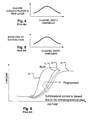
- Figure 4 illustrates uneven charge trapping distribution along the channel width dimension of a prior art memory cell.
- Figure 5 illustrates uneven charge trapping distribution as shown in Figure 4 resulting in a distribution of the effective threshold voltage of the memory cell along the channel width dimension.
- Figure 6 illustrates drain current through the channel versus gate voltage I-V characteristic of a SONOS-type memory cell suffering from uneven charge trapping distribution.
- Figure 7 illustrates a cross-sectional view taken along the channel length dimension of a dielectric charge trapping memory cell including a conductive layer above the tunneling barrier dielectric structure in accordance with one embodiment.
- Figure 8 illustrates a cross-sectional view of an array of memory cells like that shown in Figure 7 taken along the channel width dimension in accordance with one embodiment.
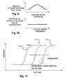
- Figure 9 illustrates an example of charge concentration across the channel width dimension of a dielectric charge trapping memory cell with a conductive layer like that illustrated in Figure 8.
- Figure 10 illustrates constant potential in the conductive layer and the effect the constant potential can have on the distribution of threshold voltage in the channel width dimension.
- Figure 11 illustrates a simulation of drain current versus gate voltage I-V characteristics of a dielectric charge trapping memory cell with a conductive layer suffering from uneven charge distribution in accordance with one embodiment.
- Figure 12 illustrates a cross-sectional view taken along the channel width dimension of a dielectric charge trapping memory cell with a conductive layer wherein the bottom dielectric structure comprises a bandgap engineered tunneling barrier structure in accordance with one embodiment.
- Figure 13 illustrates a cross-sectional view along the channel width of a dielectric charge trapping memory cell with a conductive layer wherein the charge trapping structure comprises a charge trapping layer disposed on a dielectric layer in accordance with one embodiment.
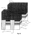
- Figure 14 illustrates a stage in the method for manufacturing a memory array comprising a stack of materials formed on a semiconductor substrate in accordance with one embodiment.
- Figure 15 illustrates a stage in the method for manufacturing a memory array comprising etching of isolation trenches and deposition of dielectric material in the isolation trenches through all layers and through all structures and into the substrate in accordance with one embodiment.
- Figure 16 illustrates a stage in the method for manufacturing a memory array comprising removal of excess oxide from the isolation trench deposition step, stripping of the hard mask layer, and removal of oxide from the top conductive layer in accordance with one embodiment.
- Figure 17 illustrates a stage in the method for manufacturing a memory array comprising the formation of additional top layer conductive material on the top conductive layer of the structure of Figure 16 for the purpose of word line definition in accordance with one embodiment.
- Figure 18 illustrates a stage in the method for fabricating a memory array comprising etching through the tunneling barrier dielectric structure and all layers and all structures disposed above the tunneling barrier dielectric structure to create rows of memory cells with word lines arranged along the rows in accordance with one embodiment.
- Figure 19 is a simplified diagram in accordance with one embodiment of an integrated circuit with an array of charge trapping memory cells and control circuitry.
- Figure 1 illustrates the basic structure of a prior art SONOS-type memory cell.
- the cell is formed on a semiconductor substrate 10 in which a first doped region 11 acts as a source terminal and a second doped region 12 acts as a drain terminal.
- a control gate 13 is formed over a charge trapping structure which includes a bottom tunneling barrier dielectric 14, a dielectric charge trapping layer 15, and a top dielectric 16.
- the channel of the memory cell is the region of the substrate 10 between the source terminal I 1 and the drain terminal 12.
- the dimension L shown in Figure 1 is typically referred to as the channel length L, because current flows between the source and drain along this dimension of the channel.
- the SONOS-type memory cell shown in Figure 1 is often configured in a NAND array configuration, in which a column in the array includes sets of memory cells arranged in series between a ground contact and a global bit line contact.
- Figure 2 illustrates a cross-sectional view of basic prior art SONOS- type memory cells taken along the channel width dimension, parallel with the word line 13 in a NAND array configuration.
- the source and drain terminals are positioned above and below the plane of the drawing of Figure 2.
- the individual columns of memory cells are separated by isolation structures, such as shallow trench isolation STI structures 20.
- the columns of memory cells can be positioned in a dense array separated by the width of a shallow trench isolation structure 20 which can be on the order of the minimum feature size F of the technology used for manufacturing the device.
- the channel width W can be on the order of the minimum feature size F for a NAND array configuration as shown.
- the electric field lines through the dielectric layers between the channel and word line 13 are illustrated, including field lines 21 and 22 on the edges of the channel.
- the field lines 21 and 22 represent fringing fields, which reduce the effectiveness of the charge trapping at the edges of the charge trapping layer 15.
- the EOT of the combination of the bottom dielectric 14, the charge trapping layer 15, and the top dielectric 16 is significantly less than the channel width W, and the fringing field effects do not substantially interfere with the operation of the device.
- the EOT is defined as being equal to the thickness of the dielectric layers scaled by the ratio of the dielectric constant of silicon dioxide to the dielectric constant of the material of the layer.
- Figure 3 illustrates a structure similar to that of Figure 2, where the channel width W is reduced to be comparable to the EOT of the combination of the bottom dielectric 54, charge trapping layer 55 and a top dielectric 56.
- the memory cell includes a polysilicon word line 53, with the columns of cells isolated by STI structures 60.
- the electric field lines 61 and 62 representing the fringing fields can have a substantial impact on the effectiveness of the charge trapping layer 55.
- non-uniform injection of charge into the charge trapping layer along the channel width due to the fringing fields can result in regions along the edges of the channel with effectively a low threshold voltage, while regions toward the center of the channel have an effectively high threshold.
- Figure 4 illustrates an uneven charge trapping distribution in the charge trapping layer along the channel width dimension of a prior art memory cell.
- the concentration of charge in the charge trapping layer is low compared to the concentration near the middle of the channel.
- the concentration of charge in the charge trapping layer is low compared to the concentration near the middle of the channel.
- Figure 5 illustrates the uneven charge trapping distribution shown in Figure 4 resulting in a distribution of the effective threshold voltage of a memory cell along the channel width dimension.
- a memory cell programmed to a high threshold state may still have low threshold regions along the edges of the cell.
- Figure 6 illustrates drain current I d through the channel versus gate voltage V g I-V characteristic of a SONOS-type cell suffering from uneven charge distribution caused by the fringing effects.
- the trace 50 on the left shows good I-V characteristics for a cell that has not been programmed and is "fresh".
- trace 51, trace 52, and trace 53 illustrate that the I-V characteristics degrade, particularly in the subthreshold region.
- the subthreshold current is pinned, marked by the dashed oval in the figure, because of the inability to trap charge at the edges of the charge trapping structure.
- Figure 7 illustrates a cross-sectional view taken along the channel length dimension L of a dielectric charge trapping memory cell 100 including a conductive layer 101 above the tunneling barrier dielectric structure 105 in accordance with one embodiment.
- the memory cell 100 includes the substrate 104 with doped region 102 and doped region 103 acting as the source and drain respectively, with doped region 102 and doped region 103 separated by a channel.
- a tunneling barrier dielectric structure 105 disposed above the channel, on the surface of the substrate 104, is a tunneling barrier dielectric structure 105 which in this example is a single dielectric layer.
- the memory cell 100 further includes a conductive layer 101 disposed above the tunneling barrier dielectric structure 105, a charge trapping structure 106 disposed above the conductive layer 101, a top dielectric structure 107 disposed above the charge trapping structure 106, and a top conductive layer 108 disposed above the top dielectric structure 107.
- the tunneling barrier structure 105 can comprise silicon dioxide or silicon oxynitride.
- the tunneling barrier dielectric structure 105 comprises silicon dioxide having a thickness on the order of 4 to 6 nm.
- the charge trapping structure 106 comprises silicon nitride, nano-particle embedded dielectrics, or other materials including "high-K” metal oxides like Al 2 O 3 , Hf 2 O 3 , etc. In certain embodiments, the charge trapping structure 106 comprises silicon nitride having a thickness on the order of 5 to 7 nm. In certain embodiments, the top dielectric structure 107 comprises silicon dioxide, or other dielectric material such as a "high-K" metal oxide like Al 2 O 3 , Hf 2 O 3 , etc. In certain embodiments, the top dielectric structure 107 comprises silicon dioxide having a thickness on the order of 5 to 9 nm.
- the conductive layer 101 may comprise p-type polysilicon, n-type polysilicon, other doped semiconductor materials, or metals such as aluminum, copper or tungsten.
- the conductive layer 101 comprises doped polysilicon having a thickness of about 2 to 6 nm.
- the conductive layer 101 is thin in preferred embodiments, so that interference caused by electric fields between the conductive layers in neighboring cells is small, and does not interfere with the performance of the memory cells, yet thick enough for reliable formation of a layer that provides for electric field distribution.
- the top conductive layer 108 may comprise p-type polysilicon, n-type polysilicon, other doped semiconductor materials, or metals such as aluminum, copper or tungsten.
- the materials chosen in these example embodiments are representative of materials that are easily manufactured. A wide variety of other materials and combinations can also be used for the memory cell layers and structures.
- Figure 8 illustrates a cross-sectional view of an array of memory cells like that shown in Figure 7 taken along the channel width dimension in accordance with one embodiment.
- the memory cells are separated by trench isolation structures 110.
- the channel width W is comparable in size to the EOT of the tunneling barrier dielectric structure 105, charge trapping structure 106, and top dielectric structure 107 in the memory cell.
- the conductive layer 101 does not affect the EOT of the memory cell because it is a conductive layer, not a dielectric.
- One characteristic of the conductive layer 101 is that it is not subject to engineering to induce a large coupling ratio like a floating gate memory cell.
- the ratio of the area of the conductive layer 101 disposed above the channel to the area of the channel can be substantially equal to the ratio of the area of the top conductive layer 108 disposed above the channel to the area of the conductive layer 101 disposed above the channel.
- the electric field above the conductive layer 101 is substantially the same as the electric field below the conductive layer 101. Even if some electrons are captured in the conductive layer 101, the large electric field applied during programming will immediately sweep all or most of the electrons into the charge trapping layer 106.
- the fringing fields 111, 112, 113 are terminated by the constant potential of the conductive layer 101.
- the fringing field effect in the charge trapping structure 106 is reduced.
- the constant potential of the conductive layer 101 will distribute the electric field uniformly across the tunneling barrier dielectric structure 105 and cause the effective distribution of threshold voltage in the channel to be more uniform in the channel width dimension.
- Figure 9 illustrates an example of charge concentration across the channel width dimension of a dielectric charge trapping memory cell with a conductive layer like that illustrated in Figure 8.
- the distribution of charge concentration for a memory cell like that illustrated in Figure 8 is similar to that of a typical SONOS-type memory cell as discussed above.
- Figure 10 illustrates the effect the conductive layer 101 can have on the distribution of threshold voltage VT in the channel width dimension.
- the constant potential in the conductive layer 101 results in an even distribution of threshold voltage in the channel width dimension. Therefore, even with an uneven distribution of charge in the charge trapping structure 106, the performance of the memory cell does not degrade substantially.
- Figure 11 illustrates a simulation of the drain current I d versus gate voltage V g I-V characteristic of a dielectric charge trapping memory cell with a conductive layer suffering from the uneven charge distribution in the charge trapping structure in accordance with one embodiment.
- the trace 80 on the left shows good I-V characteristics for a cell that has not been programmed, and is "fresh". As the programming proceeds and the charge trapped in the charge trapping structure increases, trace 81 and trace 82 illustrate that the I-V characteristics do not degrade. The subthreshold current behavior remains consistent as the threshold voltage increases.
- Figure 12 illustrates a cross-sectional view along the channel width dimension of an alternative embodiment of a dielectric charge trapping memory cell with a conductive layer.
- the memory cell 211 includes the substrate 207 with channel and doped regions acting as source and drain, isolated from adjacent devices by trench isolation structures 209, 210.
- a tunneling barrier dielectric structure 200 disposed above the channel, on the surface of the substrate 207, is a tunneling barrier dielectric structure 200 comprising a bandgap engineered tunneling barrier structure consisting in this example of a thin silicon dioxide layer 201, a thin silicon nitride layer 202, and a thin silicon dioxide layer 203.
- the memory cell 211 further includes a conductive layer 204 disposed above the tunneling barrier dielectric structure 200, a charge trapping structure 205 disposed above the conductive layer 204, a top dielectric structure 206 disposed above the charge trapping structure 205, and a top conductive layer 208 disposed above the top dielectric structure 206.
- the conductive layer 204 may comprise p-type polysilicon, n-type polysilicon, other doped semiconductor materials, or metals such as aluminum, copper, or tungsten.
- the conductive layer 204 is thin in preferred embodiments, so that interference caused by electric fields between the conductive layers in neighboring cells is small, and does not interfere with the performance of the memory cells, yet thick enough for reliable formation of a layer that provides for electric field distribution.
- the charge trapping structure 205 comprises silicon nitride, nano-particle embedded dielectrics, or other materials including "high-K" metal oxides like Al 2 O 3 , Hf 2 O 3 , etc.
- the top dielectric structure 206 comprises silicon dioxide, or other dielectric material such as a "high-K” metal oxide like Al 2 O 3 , Hf 2 O 3 , etc.
- the top conductive layer 208 may comprise p-type polysilicon, n-type polysilicon, other doped semiconductor materials, or metals such as aluminum, copper or tungsten.
- the materials chosen in these example embodiments are representative of materials that are easily manufactured. A wide variety of other materials and combinations can also be used for the memory cell layers and structures.
- the embodiment of Figure 12 having a bandgap-engineered tunneling barrier structure can be erased efficiently using a biasing arrangement that causes hole tunneling.
- Figure 13 illustrates a cross-section along the channel width dimension of yet another alternative embodiment of a dielectric charge trapping memory cell 259 with a conductive layer 251.
- the memory cell 259 includes the substrate 257 with channel with doped regions acting as source and drain, isolated from adjacent devices by trench isolation structures 255, 256.
- a tunneling barrier dielectric structure 250 disposed above the channel, on the surface of the substrate 257, is a tunneling barrier dielectric structure 250 which in this example is a single dielectric layer having an EOT greater than about 3 nm.
- the memory cell 259 further includes a conductive layer 251 disposed above the tunneling barrier dielectric structure 250, a charge trapping structure disposed above the conductive layer 251 which in this example the charge trapping structure comprises a bottom dielectric layer 252 and a charge trapping layer 253 disposed above the bottom dielectric layer 252, a top dielectric structure 254 disposed above the charge trapping layer 253, and a top conductive layer 258 disposed above the top dielectric structure 254.
- the tunneling barrier structure 250 can comprise silicon dioxide or silicon oxynitride.
- the bottom dielectric layer 252 comprises silicon dioxide.
- the charge trapping layer 253 comprises silicon nitride, nano-particle embedded dielectrics, or other materials including "high-K” metal oxides like Al 2 O 3 , Hf 2 O 3 , etc.
- the top dielectric structure 254 comprises silicon dioxide, or other dielectric material such as a "high-K” metal oxide like Al 2 O 3 , Hf 2 O 3 , etc.
- the conductive layer 251 may comprise p-type polysilicon, n-type polysilicon, other doped semiconductor materials, or metals such as aluminum, copper, or tungsten.
- the conductive layer 251 is thin in preferred embodiments, so that interference caused by electric fields between the conductive layers in neighboring cells is small and does not interfere with the performance of the memory cells, yet thick enough for reliable formation of a layer that provides for electric field distribution.
- the top conductive layer 258 may comprise p-type polysilicon, n-type polysilicon, other doped semiconductor materials, or metals such as aluminum, copper or tungsten.
- the materials chosen in these example embodiments are representative of materials that are easily manufactured.
- a wide variety of other materials and combinations can be used for the top dielectric structure 254, the tunneling barrier dielectric structure 250, and for the bottom dielectric layer 252.
- the dielectric layer 252 may block possible conduction between the conductive layer 251 and the charge trapping layer 253.
- the memory cell described herein having a conductive layer and dielectric charge trapping structure can be erased using a variety of biasing arrangements.
- the cell can be biased to induce electron de-trapping from the charge trapping structure by Fowler Nordhiem tunneling through the bottom tunneling barrier dielectric layer, with a negative voltage applied between the gate and channel.
- a biasing arrangement can be applied to induce substrate hole tunneling, particularly in the embodiment of Figure 12 using a bandgap engineered tunneling barrier dielectric as the tunneling barrier dielectric structure.
- the memory cell can be programmed using a biasing arrangement including a positive voltage from the gate to the channel to induce injection of electrons by Fowler Nordhiem tunneling into the charge trapping structure, or using other biasing arrangements.
- FIGs 14-18 illustrate an embodiment of a process flow for manufacturing a NAND flash memory array, utilizing a dielectric charge trapping memory cell having a charge distribution layer as described herein.
- a first stage in accordance with one embodiment of the manufacturing process is illustrated in Figure 14, in which a stack of materials is formed on a semiconductor substrate 300.
- a tunneling barrier dielectric structure 301 which in this example comprises a tunneling barrier dielectric layer, is formed on the surface of the substrate 300.
- a conductive layer 302 is formed on the tunneling barrier dielectric structure 301.
- a charge trapping structure 303 which in this example comprises a charge trapping layer, is formed on the conductive layer 302.
- a top dielectric structure 304 which in this example is a top dielectric layer, is formed above the top charge trapping structure 303.
- a top dielectric layer 305 is formed above the top dielectric structure 304.
- a hard mask layer 306 is formed over the top dielectric layer 305.
- the tunneling barrier dielectric structure 301 comprises silicon dioxide
- the thickness of the silicon dioxide can be in the range of 3 to 6 nm.
- the conductive layer 302 comprises polysilicon
- the thickness of the polysilicon can be in the range of 2 to 6 nm.
- the thickness of the silicon nitride can be in the range of 4 to 8 nm. In certain embodiments in which the top dielectric structure 304 comprises silicon dioxide, the thickness of the silicon dioxide can be in the range of 5 to 9 nm. In certain embodiments in which the top conductive layer 305 comprises polysilicon, the thickness of the polysilicon can be about 50 nm. In certain embodiments in which the hard mask layer 306 comprises silicon nitride, the thickness of the silicon nitride can be about 100 nanometers.
- the layers deposited in this first stage of the manufacturing process can be varied for implementation of the embodiments of Figures 12 and 13 as described above, or other similar embodiments.
- Figure 15 illustrates a next stage in the manufacturing process in accordance with one embodiment of the process.
- a photolithographic process or other pattern definition process can be used to define the locations of trench isolation structures. Trenches are then etched according to the pattern. The etch goes through the hard mask layer 306, the top conductive layer 305, the top dielectric structure 304, the charge trapping structure 303, the conductive layer 302, the tunneling barrier dielectric structure 301, and into the substrate 300 to define substrate trenches for isolating the rows of memory cells.
- the gaps are filled with silicon dioxide or other dielectric material using, for example, a high density plasma HDP chemical vapor deposition technology resulting in the hat shaped structures 310, 311 on top of the hard mask layer between the trenches, and trench isolation structures 312, 313, 314 extending into the substrate 300.
- the trench isolation structure extends into the substrate by about 200 nm.
- Figure 16 illustrates a next stage in the manufacturing process.
- the embodiment illustrated in Figure 16 comprises removal of any excess oxide from the trench isolation deposition process with, for example, chemical mechanical polishing CMP, stripping of the hard mask layer, and removal of oxide from the top conductive layer 305 with, for example, a wet hydrogen fluoride solution dip etch.
- Figure 17 illustrates a next stage in the manufacturing process.
- the formation of an additional layer 315 of top conductive layer material is formed over the structure of Figure 16 for the purposes of the word line definition.
- the additional layer 315 comprises polysilicon or other conductor.
- the layer 315 is then cleaned in preparation for a lithographic step or other patterning step to define the word lines of the array.
- the pattern for the word lines is etched down at least through the conductive layer 302, or down to the substrate 300 as illustrated in Figure 18 to create rows of memory cells.
- Figure 18 illustrates a part of the resulting structure with a first word line 315-1 and a second word line 315-2 arranged along rows of memory cells.
- Source and drain terminals are then formed by implanting dopants between the word lines, defining source and drain regions on opposite sides of the word lines, and further processing including providing a dielectric fill between the word lines to isolate the conductive layers in the cells, metal layer patterning and so on is executed to finish the device.
- the channel regions of the cells implemented as shown in Figure 18 have a length between the source and drain regions (not shown) that is defined by the width of the word line 315-1, reduced typically by diffusion of dopants during the implant processes.
- the width W of the channel is defined by the spacing between the STI structures 312, 313.
- the length and the width of the channel as defined here establishes an area of the active region of the channel that is less than or equal to the width of the word line 315-1 times the spacing between the STI structures.
- the conductive layer 302 in the illustrated structure is substantially planar and has near equal areas on its top and bottom surfaces.
- the area of the conductive layer 302 is defined by the etching processes that set the spacing between the STI structures and the width of the word lines.
- the areas of the top and bottom surfaces of the conductive layer 302 are substantially equal to one another, and substantially equal to the product of the width of the word line and the spacing between the STI structures.
- the area of the top contact for the cell in this embodiment is defined by the etching processes that set the spacing between the STI structures and the width of the word lines.
- the areas of the bottom surface of the word line acting as a top contact for the cell is substantially equal to the area of the top surface of the conductive layer, defined by the product of the width of the word line and the spacing between the STI structures.
- the channel region of a representative memory cell as described herein manufactured with processes defining critical features less than 45 nm has a length between the source and the drain of less than 45 nm, and a width orthogonal to the length of less than 45 nanometers.
- manufactured with processes defining critical features less than 30 nm has a length between the source and the drain of less than 30 nm, and a width orthogonal to the length of less than 30 nanometers, and wherein the multilayer stack has an effective oxide thickness of about 20 nm or less, and the channel region a width orthogonal to the length less than 1.5 times the effective oxide thickness of the multilayer stack.
- the channel width W of the memory cell is less than 45 nm.
- the effective oxide thickness of a memory cell is based on the dielectric layers in the charge trapping structure, and in one embodiment on the order of 15 to 25 nm.
- the channel width may be less than about 1.5 times of the effective oxide thickness of the memory cell calculated as the EOT of the combination of the tunneling barrier dielectric, the charge trapping structure and the top dielectric layer, and more preferably about equal to the effective oxide thickness for the memory cell.
- Embodiments having a channel width as low as 20 nm or less, and less than the EOT of the memory cells can be implemented using photo resist trimming techniques, phase shift masking, or other sub lithographic patterning technologies.
- the memory cells can be configured in NAND arrays with channel widths less than 45 nm, and preferably on the order of the EOT of the multilayer stack.
- the thin conductive layer is above the tunneling barrier dielectric structure, and provides an equal-potential layer to make the electric field distribution even above the channel.
- the tunneling barrier dielectric structure can consist of a layer of silicon dioxide or silicon oxynitride.
- the tunneling barrier can consist of a multilayer structure.
- the effective oxide thickness of the tunneling barrier dielectric structure is greater than 3 nm thick, so that the conductive layer is not part of the tunneling barrier.
- the gate control capability is maintained for a very narrow channel width (W ⁇ EOT) device, providing device scaling below 20 nm channel width.
- Figure 19 is a simplified diagram of an integrated circuit with an array of charge trapping memory cells with conductive field distribution layers as described above between a tunneling barrier dielectric and a charge trapping structure.
- the integrated circuit 1950 includes a memory array 1900 implemented using nonvolatile memory cells as described herein using conductive layers, on a semiconductor substrate.
- the memory cells of array 1900 may be interconnected in parallel, in series, or in a virtual ground array.
- a row decoder 1901 is coupled to a plurality of word lines 1902 arranged along rows in the memory array 1900.
- Memory cells as described herein can be configured in NAND arrays, and NOR arrays, or other types of array structures.
- a column decoder 1903 is coupled to a plurality of bit lines 1904 arranged along columns in the memory array 1900.
- Addresses are supplied on bus 1905 to column decoder 1903 and row decoder 1901.
- Sense amplifiers and data-in structures in block 1906 are coupled to the column decoder 1903 via data bus 1907.
- Data is supplied via the data-in line 1911 from input/output ports on the integrated circuit 1950, or from other data sources internal or external to the integrated circuit 1950, to the data-in structures in block 1906.
- Data is supplied via the data-out line 1915 from the sense amplifiers in block 1906 to input/output ports on the integrated circuit 1950, or to other data destinations internal or external to the integrated circuit 1950.
- a bias arrangement state machine 1909 controls the application of bias arrangement supply voltages 1908, such as for the erase verify and program verify voltages, and the arrangements for programming, erasing, and reading the memory cells, such as with the band-to-band currents.
- the array may be combined on the integrated circuit with other modules, such as processors, other memory arrays, programmable logic, dedicated logic etc.
Abstract
Description
- This application claims the benefit of
U.S. Provisional Application Serial No. 60/866,661 filed 21 November 2006 U.S. Provisional Application Serial No. 60/866,569 filed 20 November 2006 - The invention relates generally to non-volatile memory devices, and in particular to flash memory cells and manufacturing of flash memory devices.
- Flash memory technology includes memory cells that store charge between the channel and gate of a field effect transistor. The charge stored affects the threshold of the transistor, and the changes in threshold due to the stored charge can be sensed to indicate data.
- One type of charge storage memory cell in widespread application is known as a floating gate memory cell. In a floating gate memory cell, a floating gate of conductive material such as polysilicon is formed over a tunnel dielectric, and an inter-poly dielectric is formed over the floating gate to isolate it from the word line or control gate of the memory cell. The geometry of the floating gate is engineered to establish a high coupling ratio for a voltage between the floating gate and channel, so that a voltage applied on the control gate will result in a stronger electric field across the tunnel dielectric than across the inter-poly dielectric. For example, floating gates are implemented using a T-shape or a U-shape, which results in a greater surface area between the control gate and the floating gate than between the floating gate and the channel, and thereby a greater capacitance between the floating gate and the control gate. Although this technology has been widely successful, as the sizes of the memory cells and the distances between them shrink, the floating gate technology starts to degrade because of interference between neighboring floating gates.
- Another type of memory cell based on storing charge between the channel and gate of a field effect transistor uses a dielectric charge trapping structure. In this type of memory cell, a dielectric charge trapping structure is formed over a tunnel dielectric which isolates the dielectric charge trapping structure from the channel, and a top dielectric layer is formed over the charge trapping structure to isolate it from the word line or gate. A representative device is known as a silicon-oxide-nitride-oxide-silicon SONOS cell.
- In memory cells using dielectric charge trapping structures, the device can be planar because there is no coupling ratio engineering involved in the design. Rather, the electric field when no charge is trapped in the charge trapping structure is equal in the tunneling dielectric and the top dielectric. Because of the planar structure, and very little coupling between adjacent cells, memory cells using dielectric charge trapping structures are forecast to overtake floating gate memory cells in importance as the minimum feature size for the manufacturing processes goes beyond about 45 nm.
- It is found that even SONOS-type memory cells can suffer performance degradation as the minimum feature size goes below about 45 nm. In particular, non-uniform injection of charge along the channel width in the dielectric charge trapping structure due to the fringing fields can result in a region along the edge of the memory cell with effectively a low threshold voltage, while regions toward the center of the channel have an effectively high threshold. The low threshold region along the edge can result in performance degradation.
- Therefore, it is desirable to maintain a more constant threshold voltage along the channel width dimension even if there is non-uniform charge concentration in the charge trapping structure along the channel width dimension.
- The present invention relates to non-volatile memory devices, and more specifically to non-volatile memory devices including a conductive layer between a tunnel dielectric and a dielectric charge trapping structure, which may have a non-uniform distribution of trapped charge across the channel. The conductive layer distributes the electric field that is affected by the charge trapped in the dielectric charge trapping layer more uniformly across the channel, and results in a more constant threshold voltage beneath the conductive layer along the channel width dimension even if there is non-uniform charge concentration in the charge trapping structure along the channel width dimension.
- Accordingly, an embodiment described herein includes a memory cell including a source region and a drain region near a surface of a substrate and separated by a channel region, a tunneling barrier dielectric structure disposed above the channel region with a thickness and dielectric characteristics sufficient to suppress direct tunneling to the charge trapping layer from the substrate by having an effective oxide thickness EOT greater than about 3 nanometers (where EOT is determined by the actual thickness of the material of the tunneling barrier dielectric structure scaled according to the ratio of the dielectric constant of silicon dioxide and the dielectric constant of the material), a conductive layer disposed above the tunneling barrier dielectric structure covering the channel region at least partially, and preferably completely in the channel width dimension, and more preferably in both the channel width and channel length dimension, a dielectric charge trapping structure disposed above the conductive layer, a top dielectric structure disposed above the charge trapping structure, and a top conductive layer disposed above the top dielectric structure. The conductive layer acts to counteract uneven charge distribution in the charge trapping layer by establishing an equipotential surface over the channel and over the tunnel dielectric, distributing the electric field affected by the charge trapped in the charge trapping layer.
- In some embodiments the tunneling barrier dielectric structure comprises silicon dioxide or silicon oxynitride. In some embodiments the tunneling barrier dielectric structure comprises a bandgap engineered tunneling barrier structure. In some embodiments the bandgap engineered tunneling barrier structure comprises multiple layers, an example of which comprises a first silicon dioxide layer, a silicon nitride layer disposed above the first silicon dioxide layer, and a second silicon dioxide layer disposed above the silicon nitride layer. In embodiments described herein the tunneling barrier dielectric structure has negligible trapping efficiency.
- The conductive layer can be doped polysilicon between 2 to 6 nanometers thick, or other similar conductive materials having conductivity sufficient to act to distribute the field over the channel region. The conductive layer is separated from other conductive materials in the device by insulating materials.
- The charge trapping structure in various embodiments comprises silicon nitride, nano-particle embedded dielectrics, or other materials including "high-K" metal oxides like Al2O3, Hf2O3, etc. In some embodiments of the memory cell described herein, the charge trapping structure over the conductive layer comprises multiple layers, an example of which comprises a bottom dielectric layer and a charge trapping layer disposed above the bottom dielectric layer.
- An integrated circuit memory device including cells implemented as described above is also described.
- A method for manufacturing a memory cell as described herein comprises forming a tunneling barrier dielectric structure on the surface of a semiconductor substrate, forming a conductive layer on the tunneling barrier dielectric structure, forming a charge trapping structure on the conductive layer, forming a top dielectric structure on the charge trapping structure, forming a top conductive layer on the dielectric structure, and forming a source region and a drain region by implanting dopants in the semiconductor substrate, such that the source region and the drain region are separated by a channel, and the channel is below the tunneling barrier dielectric structure.
- In certain embodiments a method of manufacturing includes forming a plurality of isolation structures of dielectric material between the memory cells.
- Other aspects and advantages of the present invention can be seen on review of the drawings, which are schematic.
- Figure 1 illustrates the basic structure of a prior art SONOS-type memory cell.
- Figure 2 illustrates a cross-sectional view of basic prior art SONOS-type memory cells taken along the channel width dimension, parallel with the word line in a NAND array configuration.
- Figure 3 illustrates a structure similar to Figure 2 wherein the channel width is reduced to be comparable to the effective oxide thickness of the combination of the bottom dielectric, charge trapping layer, and top dielectric.
- Figure 4 illustrates uneven charge trapping distribution along the channel width dimension of a prior art memory cell.
- Figure 5 illustrates uneven charge trapping distribution as shown in Figure 4 resulting in a distribution of the effective threshold voltage of the memory cell along the channel width dimension.
- Figure 6 illustrates drain current through the channel versus gate voltage I-V characteristic of a SONOS-type memory cell suffering from uneven charge trapping distribution.
- Figure 7 illustrates a cross-sectional view taken along the channel length dimension of a dielectric charge trapping memory cell including a conductive layer above the tunneling barrier dielectric structure in accordance with one embodiment.
- Figure 8 illustrates a cross-sectional view of an array of memory cells like that shown in Figure 7 taken along the channel width dimension in accordance with one embodiment.
- Figure 9 illustrates an example of charge concentration across the channel width dimension of a dielectric charge trapping memory cell with a conductive layer like that illustrated in Figure 8.
- Figure 10 illustrates constant potential in the conductive layer and the effect the constant potential can have on the distribution of threshold voltage in the channel width dimension.
- Figure 11 illustrates a simulation of drain current versus gate voltage I-V characteristics of a dielectric charge trapping memory cell with a conductive layer suffering from uneven charge distribution in accordance with one embodiment.
- Figure 12 illustrates a cross-sectional view taken along the channel width dimension of a dielectric charge trapping memory cell with a conductive layer wherein the bottom dielectric structure comprises a bandgap engineered tunneling barrier structure in accordance with one embodiment.
- Figure 13 illustrates a cross-sectional view along the channel width of a dielectric charge trapping memory cell with a conductive layer wherein the charge trapping structure comprises a charge trapping layer disposed on a dielectric layer in accordance with one embodiment.
- Figure 14 illustrates a stage in the method for manufacturing a memory array comprising a stack of materials formed on a semiconductor substrate in accordance with one embodiment.
- Figure 15 illustrates a stage in the method for manufacturing a memory array comprising etching of isolation trenches and deposition of dielectric material in the isolation trenches through all layers and through all structures and into the substrate in accordance with one embodiment.
- Figure 16 illustrates a stage in the method for manufacturing a memory array comprising removal of excess oxide from the isolation trench deposition step, stripping of the hard mask layer, and removal of oxide from the top conductive layer in accordance with one embodiment.
- Figure 17 illustrates a stage in the method for manufacturing a memory array comprising the formation of additional top layer conductive material on the top conductive layer of the structure of Figure 16 for the purpose of word line definition in accordance with one embodiment.
- Figure 18 illustrates a stage in the method for fabricating a memory array comprising etching through the tunneling barrier dielectric structure and all layers and all structures disposed above the tunneling barrier dielectric structure to create rows of memory cells with word lines arranged along the rows in accordance with one embodiment.
- Figure 19 is a simplified diagram in accordance with one embodiment of an integrated circuit with an array of charge trapping memory cells and control circuitry.
- A detailed description of various embodiments is provided with reference to Figures 1-19.
- Figure 1 illustrates the basic structure of a prior art SONOS-type memory cell. The cell is formed on a
semiconductor substrate 10 in which a firstdoped region 11 acts as a source terminal and a seconddoped region 12 acts as a drain terminal. Acontrol gate 13 is formed over a charge trapping structure which includes a bottom tunneling barrier dielectric 14, a dielectriccharge trapping layer 15, and a top dielectric 16. The channel of the memory cell is the region of thesubstrate 10 between the source terminal I 1 and thedrain terminal 12. The dimension L shown in Figure 1 is typically referred to as the channel length L, because current flows between the source and drain along this dimension of the channel. The SONOS-type memory cell shown in Figure 1 is often configured in a NAND array configuration, in which a column in the array includes sets of memory cells arranged in series between a ground contact and a global bit line contact. - Figure 2 illustrates a cross-sectional view of basic prior art SONOS- type memory cells taken along the channel width dimension, parallel with the
word line 13 in a NAND array configuration. For perspective, the source and drain terminals are positioned above and below the plane of the drawing of Figure 2. The individual columns of memory cells are separated by isolation structures, such as shallow trenchisolation STI structures 20. In this manner, the columns of memory cells can be positioned in a dense array separated by the width of a shallowtrench isolation structure 20 which can be on the order of the minimum feature size F of the technology used for manufacturing the device. Likewise, the channel width W can be on the order of the minimum feature size F for a NAND array configuration as shown. In Figure 2, the electric field lines through the dielectric layers between the channel andword line 13 are illustrated, includingfield lines charge trapping layer 15. In the embodiment illustrated in Figure 2, the EOT of the combination of thebottom dielectric 14, thecharge trapping layer 15, and the top dielectric 16 (typically on the order of 20 nm) is significantly less than the channel width W, and the fringing field effects do not substantially interfere with the operation of the device. The EOT is defined as being equal to the thickness of the dielectric layers scaled by the ratio of the dielectric constant of silicon dioxide to the dielectric constant of the material of the layer. - It is found that even SONOS-type memory cells can suffer performance degradation as the minimum feature size goes below about 45 nm. For example, Figure 3 illustrates a structure similar to that of Figure 2, where the channel width W is reduced to be comparable to the EOT of the combination of the
bottom dielectric 54, charge trapping layer 55 and atop dielectric 56. In this embodiment the memory cell includes apolysilicon word line 53, with the columns of cells isolated bySTI structures 60. In this embodiment theelectric field lines - Figure 4 illustrates an uneven charge trapping distribution in the charge trapping layer along the channel width dimension of a prior art memory cell. As can be seen in Figure 4, on the left side of the channel the concentration of charge in the charge trapping layer is low compared to the concentration near the middle of the channel. Also, on the right side of the channel, the concentration of charge in the charge trapping layer is low compared to the concentration near the middle of the channel. Figure 5 illustrates the uneven charge trapping distribution shown in Figure 4 resulting in a distribution of the effective threshold voltage of a memory cell along the channel width dimension. Thus a memory cell programmed to a high threshold state may still have low threshold regions along the edges of the cell. Figure 6 illustrates drain current Id through the channel versus gate voltage Vg I-V characteristic of a SONOS-type cell suffering from uneven charge distribution caused by the fringing effects. The
trace 50 on the left shows good I-V characteristics for a cell that has not been programmed and is "fresh". As the programming proceeds and the charge trapped in the charge trapping layer increases,trace 51,trace 52, and trace 53 illustrate that the I-V characteristics degrade, particularly in the subthreshold region. The subthreshold current is pinned, marked by the dashed oval in the figure, because of the inability to trap charge at the edges of the charge trapping structure. - Figure 7 illustrates a cross-sectional view taken along the channel length dimension L of a dielectric charge trapping
memory cell 100 including aconductive layer 101 above the tunneling barrierdielectric structure 105 in accordance with one embodiment. In the embodiment illustrated in Figure 7, thememory cell 100 includes thesubstrate 104 with dopedregion 102 and dopedregion 103 acting as the source and drain respectively, with dopedregion 102 and dopedregion 103 separated by a channel. In the embodiment illustrated in Figure 7, disposed above the channel, on the surface of thesubstrate 104, is a tunneling barrierdielectric structure 105 which in this example is a single dielectric layer. In the embodiment illustrated in Figure 7, thememory cell 100 further includes aconductive layer 101 disposed above the tunneling barrierdielectric structure 105, a charge trapping structure 106 disposed above theconductive layer 101, atop dielectric structure 107 disposed above the charge trapping structure 106, and a topconductive layer 108 disposed above thetop dielectric structure 107. In certain embodiments, thetunneling barrier structure 105 can comprise silicon dioxide or silicon oxynitride. In certain embodiments, the tunneling barrierdielectric structure 105 comprises silicon dioxide having a thickness on the order of 4 to 6 nm. In certain embodiments the charge trapping structure 106 comprises silicon nitride, nano-particle embedded dielectrics, or other materials including "high-K" metal oxides like Al2O3, Hf2O3, etc. In certain embodiments, the charge trapping structure 106 comprises silicon nitride having a thickness on the order of 5 to 7 nm. In certain embodiments, thetop dielectric structure 107 comprises silicon dioxide, or other dielectric material such as a "high-K" metal oxide like Al2O3, Hf2O3, etc. In certain embodiments, thetop dielectric structure 107 comprises silicon dioxide having a thickness on the order of 5 to 9 nm. Also, in certain embodiments theconductive layer 101 may comprise p-type polysilicon, n-type polysilicon, other doped semiconductor materials, or metals such as aluminum, copper or tungsten. In a representative embodiment, theconductive layer 101 comprises doped polysilicon having a thickness of about 2 to 6 nm. Theconductive layer 101 is thin in preferred embodiments, so that interference caused by electric fields between the conductive layers in neighboring cells is small, and does not interfere with the performance of the memory cells, yet thick enough for reliable formation of a layer that provides for electric field distribution. In certain embodiments the topconductive layer 108 may comprise p-type polysilicon, n-type polysilicon, other doped semiconductor materials, or metals such as aluminum, copper or tungsten. The materials chosen in these example embodiments are representative of materials that are easily manufactured. A wide variety of other materials and combinations can also be used for the memory cell layers and structures. - Figure 8 illustrates a cross-sectional view of an array of memory cells like that shown in Figure 7 taken along the channel width dimension in accordance with one embodiment. In the embodiment illustrated in Figure 8, the memory cells are separated by
trench isolation structures 110. In the embodiment illustrated in Figure 8, the channel width W is comparable in size to the EOT of the tunneling barrierdielectric structure 105, charge trapping structure 106, andtop dielectric structure 107 in the memory cell. Theconductive layer 101 does not affect the EOT of the memory cell because it is a conductive layer, not a dielectric. One characteristic of theconductive layer 101 is that it is not subject to engineering to induce a large coupling ratio like a floating gate memory cell. Rather, the ratio of the area of theconductive layer 101 disposed above the channel to the area of the channel can be substantially equal to the ratio of the area of the topconductive layer 108 disposed above the channel to the area of theconductive layer 101 disposed above the channel. In this manner, the electric field above theconductive layer 101 is substantially the same as the electric field below theconductive layer 101. Even if some electrons are captured in theconductive layer 101, the large electric field applied during programming will immediately sweep all or most of the electrons into the charge trapping layer 106. - As illustrated in Figure 8, the fringing fields 111, 112, 113 are terminated by the constant potential of the
conductive layer 101. Thus, the fringing field effect in the charge trapping structure 106 is reduced. Furthermore, to the extent that a nonuniform distribution of charge occurs in a memory cell like that illustrated in Figure 8, the constant potential of theconductive layer 101 will distribute the electric field uniformly across the tunneling barrierdielectric structure 105 and cause the effective distribution of threshold voltage in the channel to be more uniform in the channel width dimension. - Figure 9 illustrates an example of charge concentration across the channel width dimension of a dielectric charge trapping memory cell with a conductive layer like that illustrated in Figure 8. For this example, the distribution of charge concentration for a memory cell like that illustrated in Figure 8 is similar to that of a typical SONOS-type memory cell as discussed above. Figure 10 illustrates the effect the
conductive layer 101 can have on the distribution of threshold voltage VT in the channel width dimension. As illustrated in Figure 10, the constant potential in theconductive layer 101 results in an even distribution of threshold voltage in the channel width dimension. Therefore, even with an uneven distribution of charge in the charge trapping structure 106, the performance of the memory cell does not degrade substantially. - Figure 11 illustrates a simulation of the drain current Id versus gate voltage Vg I-V characteristic of a dielectric charge trapping memory cell with a conductive layer suffering from the uneven charge distribution in the charge trapping structure in accordance with one embodiment. The
trace 80 on the left shows good I-V characteristics for a cell that has not been programmed, and is "fresh". As the programming proceeds and the charge trapped in the charge trapping structure increases,trace 81 andtrace 82 illustrate that the I-V characteristics do not degrade. The subthreshold current behavior remains consistent as the threshold voltage increases. - Figure 12 illustrates a cross-sectional view along the channel width dimension of an alternative embodiment of a dielectric charge trapping memory cell with a conductive layer. In the embodiment illustrated in Figure 12, the
memory cell 211 includes thesubstrate 207 with channel and doped regions acting as source and drain, isolated from adjacent devices bytrench isolation structures substrate 207, is a tunneling barrierdielectric structure 200 comprising a bandgap engineered tunneling barrier structure consisting in this example of a thinsilicon dioxide layer 201, a thinsilicon nitride layer 202, and a thinsilicon dioxide layer 203. In the embodiment illustrated in Figure 12, thememory cell 211 further includes aconductive layer 204 disposed above the tunneling barrierdielectric structure 200, acharge trapping structure 205 disposed above theconductive layer 204, atop dielectric structure 206 disposed above thecharge trapping structure 205, and a topconductive layer 208 disposed above thetop dielectric structure 206. In certain embodiments theconductive layer 204 may comprise p-type polysilicon, n-type polysilicon, other doped semiconductor materials, or metals such as aluminum, copper, or tungsten. Theconductive layer 204 is thin in preferred embodiments, so that interference caused by electric fields between the conductive layers in neighboring cells is small, and does not interfere with the performance of the memory cells, yet thick enough for reliable formation of a layer that provides for electric field distribution. In certain embodiments thecharge trapping structure 205 comprises silicon nitride, nano-particle embedded dielectrics, or other materials including "high-K" metal oxides like Al2O3, Hf2O3, etc. In certain embodiments, thetop dielectric structure 206 comprises silicon dioxide, or other dielectric material such as a "high-K" metal oxide like Al2O3, Hf2O3, etc. In certain embodiments the topconductive layer 208 may comprise p-type polysilicon, n-type polysilicon, other doped semiconductor materials, or metals such as aluminum, copper or tungsten. The materials chosen in these example embodiments are representative of materials that are easily manufactured. A wide variety of other materials and combinations can also be used for the memory cell layers and structures. The embodiment of Figure 12 having a bandgap-engineered tunneling barrier structure can be erased efficiently using a biasing arrangement that causes hole tunneling. - Figure 13 illustrates a cross-section along the channel width dimension of yet another alternative embodiment of a dielectric charge trapping
memory cell 259 with aconductive layer 251. In the embodiment illustrated in Figure 13, thememory cell 259 includes thesubstrate 257 with channel with doped regions acting as source and drain, isolated from adjacent devices bytrench isolation structures substrate 257, is a tunneling barrierdielectric structure 250 which in this example is a single dielectric layer having an EOT greater than about 3 nm. In the embodiment illustrated in Figure 13, thememory cell 259 further includes aconductive layer 251 disposed above the tunneling barrierdielectric structure 250, a charge trapping structure disposed above theconductive layer 251 which in this example the charge trapping structure comprises abottom dielectric layer 252 and acharge trapping layer 253 disposed above thebottom dielectric layer 252, atop dielectric structure 254 disposed above thecharge trapping layer 253, and a topconductive layer 258 disposed above thetop dielectric structure 254. In certain embodiments, thetunneling barrier structure 250 can comprise silicon dioxide or silicon oxynitride. In certain embodiments, thebottom dielectric layer 252 comprises silicon dioxide. In certain embodiments, thecharge trapping layer 253 comprises silicon nitride, nano-particle embedded dielectrics, or other materials including "high-K" metal oxides like Al2O3, Hf2O3, etc. In certain embodiments, thetop dielectric structure 254 comprises silicon dioxide, or other dielectric material such as a "high-K" metal oxide like Al2O3, Hf2O3, etc. Also, in certain embodiments theconductive layer 251 may comprise p-type polysilicon, n-type polysilicon, other doped semiconductor materials, or metals such as aluminum, copper, or tungsten. Theconductive layer 251 is thin in preferred embodiments, so that interference caused by electric fields between the conductive layers in neighboring cells is small and does not interfere with the performance of the memory cells, yet thick enough for reliable formation of a layer that provides for electric field distribution. In certain embodiments the topconductive layer 258 may comprise p-type polysilicon, n-type polysilicon, other doped semiconductor materials, or metals such as aluminum, copper or tungsten. The materials chosen in these example embodiments are representative of materials that are easily manufactured. A wide variety of other materials and combinations can be used for thetop dielectric structure 254, the tunneling barrierdielectric structure 250, and for thebottom dielectric layer 252. Thedielectric layer 252 may block possible conduction between theconductive layer 251 and thecharge trapping layer 253. - The memory cell described herein having a conductive layer and dielectric charge trapping structure can be erased using a variety of biasing arrangements. For example, the cell can be biased to induce electron de-trapping from the charge trapping structure by Fowler Nordhiem tunneling through the bottom tunneling barrier dielectric layer, with a negative voltage applied between the gate and channel. In alternative embodiments, a biasing arrangement can be applied to induce substrate hole tunneling, particularly in the embodiment of Figure 12 using a bandgap engineered tunneling barrier dielectric as the tunneling barrier dielectric structure. The memory cell can be programmed using a biasing arrangement including a positive voltage from the gate to the channel to induce injection of electrons by Fowler Nordhiem tunneling into the charge trapping structure, or using other biasing arrangements.
- Figures 14-18 illustrate an embodiment of a process flow for manufacturing a NAND flash memory array, utilizing a dielectric charge trapping memory cell having a charge distribution layer as described herein. A first stage in accordance with one embodiment of the manufacturing process is illustrated in Figure 14, in which a stack of materials is formed on a
semiconductor substrate 300. First, a tunneling barrierdielectric structure 301, which in this example comprises a tunneling barrier dielectric layer, is formed on the surface of thesubstrate 300. Next, aconductive layer 302 is formed on the tunneling barrierdielectric structure 301. Next, acharge trapping structure 303, which in this example comprises a charge trapping layer, is formed on theconductive layer 302. Then, atop dielectric structure 304, which in this example is a top dielectric layer, is formed above the topcharge trapping structure 303. Next, atop dielectric layer 305 is formed above thetop dielectric structure 304. In the embodiment illustrated in Figure 14, next ahard mask layer 306 is formed over thetop dielectric layer 305. In certain embodiments in which the tunneling barrierdielectric structure 301 comprises silicon dioxide, the thickness of the silicon dioxide can be in the range of 3 to 6 nm. In certain embodiments in which theconductive layer 302 comprises polysilicon, the thickness of the polysilicon can be in the range of 2 to 6 nm. In certain embodiments in which thecharge trapping structure 303 comprises silicon nitride, the thickness of the silicon nitride can be in the range of 4 to 8 nm. In certain embodiments in which thetop dielectric structure 304 comprises silicon dioxide, the thickness of the silicon dioxide can be in the range of 5 to 9 nm. In certain embodiments in which the topconductive layer 305 comprises polysilicon, the thickness of the polysilicon can be about 50 nm. In certain embodiments in which thehard mask layer 306 comprises silicon nitride, the thickness of the silicon nitride can be about 100 nanometers. The layers deposited in this first stage of the manufacturing process can be varied for implementation of the embodiments of Figures 12 and 13 as described above, or other similar embodiments. - Figure 15 illustrates a next stage in the manufacturing process in accordance with one embodiment of the process. In this stage, a photolithographic process or other pattern definition process can be used to define the locations of trench isolation structures. Trenches are then etched according to the pattern. The etch goes through the
hard mask layer 306, the topconductive layer 305, thetop dielectric structure 304, thecharge trapping structure 303, theconductive layer 302, the tunneling barrierdielectric structure 301, and into thesubstrate 300 to define substrate trenches for isolating the rows of memory cells. Next, the gaps are filled with silicon dioxide or other dielectric material using, for example, a high density plasma HDP chemical vapor deposition technology resulting in the hat shapedstructures trench isolation structures substrate 300. In certain embodiments the trench isolation structure extends into the substrate by about 200 nm. - Figure 16 illustrates a next stage in the manufacturing process. The embodiment illustrated in Figure 16 comprises removal of any excess oxide from the trench isolation deposition process with, for example, chemical mechanical polishing CMP, stripping of the hard mask layer, and removal of oxide from the top
conductive layer 305 with, for example, a wet hydrogen fluoride solution dip etch. - Figure 17 illustrates a next stage in the manufacturing process. In this stage, the formation of an
additional layer 315 of top conductive layer material is formed over the structure of Figure 16 for the purposes of the word line definition. In certain embodiments theadditional layer 315 comprises polysilicon or other conductor. Thelayer 315 is then cleaned in preparation for a lithographic step or other patterning step to define the word lines of the array. The pattern for the word lines is etched down at least through theconductive layer 302, or down to thesubstrate 300 as illustrated in Figure 18 to create rows of memory cells. - Figure 18 illustrates a part of the resulting structure with a first word line 315-1 and a second word line 315-2 arranged along rows of memory cells. Source and drain terminals are then formed by implanting dopants between the word lines, defining source and drain regions on opposite sides of the word lines, and further processing including providing a dielectric fill between the word lines to isolate the conductive layers in the cells, metal layer patterning and so on is executed to finish the device.
- The channel regions of the cells implemented as shown in Figure 18 have a length between the source and drain regions (not shown) that is defined by the width of the word line 315-1, reduced typically by diffusion of dopants during the implant processes. The width W of the channel is defined by the spacing between the
STI structures - The
conductive layer 302 in the illustrated structure is substantially planar and has near equal areas on its top and bottom surfaces. The area of theconductive layer 302 is defined by the etching processes that set the spacing between the STI structures and the width of the word lines. Thus, the areas of the top and bottom surfaces of theconductive layer 302 are substantially equal to one another, and substantially equal to the product of the width of the word line and the spacing between the STI structures. Likewise, the area of the top contact for the cell in this embodiment is defined by the etching processes that set the spacing between the STI structures and the width of the word lines. Thus, the areas of the bottom surface of the word line acting as a top contact for the cell is substantially equal to the area of the top surface of the conductive layer, defined by the product of the width of the word line and the spacing between the STI structures. - As can be seen from the perspective view in Figure 18, the channel region of a representative memory cell as described herein manufactured with processes defining critical features less than 45 nm, has a length between the source and the drain of less than 45 nm, and a width orthogonal to the length of less than 45 nanometers.
- In representative embodiments manufactured with processes defining critical features less than 30 nm, has a length between the source and the drain of less than 30 nm, and a width orthogonal to the length of less than 30 nanometers, and wherein the multilayer stack has an effective oxide thickness of about 20 nm or less, and the channel region a width orthogonal to the length less than 1.5 times the effective oxide thickness of the multilayer stack.
- In a representative embodiment, the channel width W of the memory cell is less than 45 nm. The effective oxide thickness of a memory cell is based on the dielectric layers in the charge trapping structure, and in one embodiment on the order of 15 to 25 nm. For memory cells having this structure, the channel width may be less than about 1.5 times of the effective oxide thickness of the memory cell calculated as the EOT of the combination of the tunneling barrier dielectric, the charge trapping structure and the top dielectric layer, and more preferably about equal to the effective oxide thickness for the memory cell. Embodiments having a channel width as low as 20 nm or less, and less than the EOT of the memory cells can be implemented using photo resist trimming techniques, phase shift masking, or other sub lithographic patterning technologies.
- In certain embodiments, the memory cells can be configured in NAND arrays with channel widths less than 45 nm, and preferably on the order of the EOT of the multilayer stack. The thin conductive layer is above the tunneling barrier dielectric structure, and provides an equal-potential layer to make the electric field distribution even above the channel. The tunneling barrier dielectric structure can consist of a layer of silicon dioxide or silicon oxynitride. Alternatively, the tunneling barrier can consist of a multilayer structure. In embodiments of the memory cell described herein, the effective oxide thickness of the tunneling barrier dielectric structure, whether it is a single layer or multilayer structure, is greater than 3 nm thick, so that the conductive layer is not part of the tunneling barrier. The gate control capability is maintained for a very narrow channel width (W<EOT) device, providing device scaling below 20 nm channel width.
- Figure 19 is a simplified diagram of an integrated circuit with an array of charge trapping memory cells with conductive field distribution layers as described above between a tunneling barrier dielectric and a charge trapping structure. The
integrated circuit 1950 includes amemory array 1900 implemented using nonvolatile memory cells as described herein using conductive layers, on a semiconductor substrate. The memory cells ofarray 1900 may be interconnected in parallel, in series, or in a virtual ground array. Arow decoder 1901 is coupled to a plurality ofword lines 1902 arranged along rows in thememory array 1900. Memory cells as described herein can be configured in NAND arrays, and NOR arrays, or other types of array structures. Acolumn decoder 1903 is coupled to a plurality ofbit lines 1904 arranged along columns in thememory array 1900. Addresses are supplied onbus 1905 tocolumn decoder 1903 androw decoder 1901. Sense amplifiers and data-in structures inblock 1906 are coupled to thecolumn decoder 1903 viadata bus 1907. Data is supplied via the data-inline 1911 from input/output ports on theintegrated circuit 1950, or from other data sources internal or external to theintegrated circuit 1950, to the data-in structures inblock 1906. Data is supplied via the data-out line 1915 from the sense amplifiers inblock 1906 to input/output ports on theintegrated circuit 1950, or to other data destinations internal or external to theintegrated circuit 1950. A biasarrangement state machine 1909 controls the application of biasarrangement supply voltages 1908, such as for the erase verify and program verify voltages, and the arrangements for programming, erasing, and reading the memory cells, such as with the band-to-band currents. The array may be combined on the integrated circuit with other modules, such as processors, other memory arrays, programmable logic, dedicated logic etc. - While the present invention is disclosed by reference to the preferred embodiments and examples detailed above, it is to be understood that these examples are intended in an illustrative rather than a limiting sense. It is to be understood and appreciated that that the fabrication steps and structures described herein do not cover a complete process flow for the manufacture of entire integrated circuits. The present invention may be practiced in conjunction with various integrated circuit fabrication techniques that are known in the art or to be developed. It is contemplated that modifications and combinations will readily occur to those skilled in the art, which modifications and combinations will be within the spirit of the invention and the scope of the following claims.
Claims (27)
- A memory cell comprising:a semiconductor substrate having a surface with a source region and a drain region in the substrate and separated by a channel region;a multilayer stack over the channel including a tunneling barrier dielectric structure with an effective oxide thickness of greater than 3 nanometers disposed on the surface of the substrate above the channel region, a conductive layer disposed above the tunneling barrier dielectric structure and above the channel region, a charge trapping structure disposed above the conductive layer and above the channel region, and a top dielectric structure disposed above the charge trapping structure and above the channel region; anda top conductive layer disposed above the top dielectric structure and above the channel region.
- A memory cell according to claim 1, wherein the channel region has a length between the source and the drain, and a width orthogonal to the length of less than 45 nanometers.
- A memory cell according to claim 1 or claim 2, wherein the multilayer stack has an effective oxide thickness and the channel region has a length between the source and the drain, and a width orthogonal to the length less than 1.5 times the effective oxide thickness of the multilayer stack.
- A memory cell according to claim 1, wherein the channel region has an active area with a length between the source and the drain, and a width orthogonal to the length, and the conductive layer has a width that is substantially equal to the width of the active area of the channel region.
- A memory cell according to any preceding claim, wherein the tunnelling barrier dielectric structure comprises silicon dioxide.
- A memory cell according to claims 1 to 4, wherein the tunnelling barrier dielectric structure comprises silicon oxynitride.
- A memory cell according to any preceding claim, wherein the tunnelling barrier dielectric structure comprises a bandgap engineered tunnelling barrier structure.
- A memory cell according to any preceding claim, wherein the conductive layer comprises doped semiconductor material.
- A memory cell according to any preceding claim, wherein the conductive layer comprises doped polysilicon having a thickness less than 6 nanometers.
- A memory cell according to any preceding claim, wherein the conductive layer comprises metal.
- A memory cell according to any preceding claim, wherein the charge trapping structure comprises silicon nitride.
- A memory cell according to any of claims 1 to 10, wherein the charge trapping structure comprises a silicon dioxide layer and a silicon nitride layer disposed above the silicon dioxide layer.
- A memory device comprising:an array of memory cells on a semiconductor substrate;the memory cells comprising a source region and a drain region in the substrate and separated by a channel region, a tunneling barrier dielectric structure with an effective oxide thickness of greater than 3 nanometers disposed above the channel region, a conductive layer disposed above the tunneling barrier dielectric structure and above the channel region, a charge trapping structure disposed above the conductive layer and above the channel region, a top dielectric structure disposed above the charge trapping structure, and a top conductive layer disposed above the top dielectric structure and above the channel region;a row decoder;a column decoder;sense amplifiers;at least one input port;at least one output port;data-in structures; andbias arrangement state machine.
- A method for manufacturing a memory cell, the method comprising:forming a tunneling barrier dielectric structure with an effective oxide thickness of greater than 3 nanometers on the surface of a semiconductor substrate, forming a conductive layer on the tunneling barrier dielectric structure, forming a charge trapping structure on the conductive layer, forming a top dielectric structure on the charge trapping structure, forming a top conductive layer on the top dielectric structure; andforming a source region and a drain region by implanting dopants in the surface of the semiconductor substrate, such that the source region and the drain region are separated by a channel region, and the channel region is below the tunneling barrier dielectric structure.
- A method according to claim 14, including manufacturing a memory array comprising forming a plurality of the memory cells.
- A method according to claim 14 or 15, wherein the tunnelling barrier dielectric structure comprises silicon dioxide having a thickness in the range of 3 to 6 nanometers.
- A method according to any of claims 14 to 16, wherein the forming a tunnelling barrier dielectric structure comprises forming a bandgap engineered tunnelling barrier structure by forming a plurality of dielectric layers.
- A method according to any of claims 14 to 17, wherein the conductive layer comprises polysilicon having a thickness less than 6 nanometers.
- A method according to any of claims 14 to 18, wherein the charge trapping structure comprises silicon nitride having a thickness in a range of 4 to 8 nanometers.
- A method according to any of claims 14 to 19, wherein the forming a tunnelling barrier dielectric structure comprises forming a dielectric layer and forming a charge trapping layer on the dielectric layer.
- A method according to any of claims 14 to 20, wherein the top dielectric structure comprises silicon dioxide having a thickness in the range of 5 to 9 nanometers.
- A method according to any of claims 14 to 20, wherein the top conductive layer comprises polysilicon having a thickness of about 50 nanometers.
- A method for manufacturing an array of memory cells, the method comprising:forming a tunneling barrier dielectric structure with an effective oxide thickness of greater than 3 nanometers on the surface of a semiconductor substrate, forming a conductive layer on the tunneling barrier dielectric structure, forming a charge trapping structure on the conductive layer, forming a top dielectric structure on the charge trapping structure, forming a top conductive layer on the top dielectric structure, forming a hard mask layer on the top conductive layer;forming a plurality of isolation structures of dielectric material between a plurality of memory cells through all the layers and all the structures and into the substrate;stripping of the hard mask layer;forming a plurality of rows of memory cells by etching through the tunneling barrier dielectric structure and all the layers and all the structures disposed above the tunneling barrier dielectric structure; andforming source regions and drain regions by implanting dopants in the surface of the semiconductor substrate, such pairs of the source region and the drain region are separated by a memory cell channel region, and the channel region is below the tunneling barrier dielectric structure.
- A method according to claim 23, wherein the hard mask layer comprises silicon nitride having a thickness of about 100 nanometers.
- A method according to claim 23 or claim 24, wherein the isolation structures of dielectric material comprise silicon dioxide.
- A method according to any of claims 23 to 25, including removing excess oxide due to forming of the plurality of isolation structures comprising chemical mechanical polishing.
- A method according to any of claims 23 to 26, including removing oxide from the top conductive layer after the stripping of the hard mask layer comprising wet hydrogen fluoride solution dip etch.
Applications Claiming Priority (3)
| Application Number | Priority Date | Filing Date | Title |
|---|---|---|---|
| US86658906P | 2006-11-20 | 2006-11-20 | |
| US86666106P | 2006-11-21 | 2006-11-21 | |
| US11/756,559 US8101989B2 (en) | 2006-11-20 | 2007-05-31 | Charge trapping devices with field distribution layer over tunneling barrier |
Publications (3)
| Publication Number | Publication Date |
|---|---|
| EP1923909A2 true EP1923909A2 (en) | 2008-05-21 |
| EP1923909A3 EP1923909A3 (en) | 2009-12-09 |
| EP1923909B1 EP1923909B1 (en) | 2016-11-16 |
Family
ID=39111468
Family Applications (1)
| Application Number | Title | Priority Date | Filing Date |
|---|---|---|---|
| EP07252779.9A Active EP1923909B1 (en) | 2006-11-20 | 2007-07-11 | Charge trapping memory device and manufacturing method thereof |
Country Status (6)
| Country | Link |
|---|---|
| US (2) | US8101989B2 (en) |
| EP (1) | EP1923909B1 (en) |
| JP (2) | JP5294590B2 (en) |
| KR (2) | KR100933905B1 (en) |
| CN (1) | CN101188251B (en) |
| TW (1) | TWI351756B (en) |
Families Citing this family (23)
| Publication number | Priority date | Publication date | Assignee | Title |
|---|---|---|---|---|
| US8482052B2 (en) | 2005-01-03 | 2013-07-09 | Macronix International Co., Ltd. | Silicon on insulator and thin film transistor bandgap engineered split gate memory |
| US7763927B2 (en) | 2005-12-15 | 2010-07-27 | Macronix International Co., Ltd. | Non-volatile memory device having a nitride-oxide dielectric layer |
| US7692223B2 (en) * | 2006-04-28 | 2010-04-06 | Semiconductor Energy Laboratory Co., Ltd | Semiconductor device and method for manufacturing the same |
| US7746694B2 (en) * | 2006-07-10 | 2010-06-29 | Macronix International Co., Ltd. | Nonvolatile memory array having modified channel region interface |
| US7838923B2 (en) * | 2007-08-09 | 2010-11-23 | Macronix International Co., Ltd. | Lateral pocket implant charge trapping devices |
| US7816727B2 (en) * | 2007-08-27 | 2010-10-19 | Macronix International Co., Ltd. | High-κ capped blocking dielectric bandgap engineered SONOS and MONOS |
| US7643349B2 (en) * | 2007-10-18 | 2010-01-05 | Macronix International Co., Ltd. | Efficient erase algorithm for SONOS-type NAND flash |
| US7848148B2 (en) * | 2007-10-18 | 2010-12-07 | Macronix International Co., Ltd. | One-transistor cell semiconductor on insulator random access memory |
| US7768838B2 (en) * | 2007-10-30 | 2010-08-03 | Micron Technology, Inc. | Operating memory cells |
| US8008707B2 (en) | 2007-12-14 | 2011-08-30 | Kabushiki Kaisha Toshiba | Nonvolatile semiconductor memory device provided with charge storage layer in memory cell |
| US7973357B2 (en) * | 2007-12-20 | 2011-07-05 | Samsung Electronics Co., Ltd. | Non-volatile memory devices |
| US8068370B2 (en) * | 2008-04-18 | 2011-11-29 | Macronix International Co., Ltd. | Floating gate memory device with interpoly charge trapping structure |
| US8081516B2 (en) * | 2009-01-02 | 2011-12-20 | Macronix International Co., Ltd. | Method and apparatus to suppress fringing field interference of charge trapping NAND memory |
| US8861273B2 (en) * | 2009-04-21 | 2014-10-14 | Macronix International Co., Ltd. | Bandgap engineered charge trapping memory in two-transistor nor architecture |
| JP2011071240A (en) * | 2009-09-24 | 2011-04-07 | Toshiba Corp | Semiconductor storage device and method for manufacturing the same |
| KR101102406B1 (en) * | 2010-06-15 | 2012-01-05 | 서울대학교산학협력단 | Single-electron transistor having charge storage layer and fabrication method of the same |
| US8916920B2 (en) * | 2011-07-19 | 2014-12-23 | Macronix International Co., Ltd. | Memory structure with planar upper surface |
| US9559113B2 (en) | 2014-05-01 | 2017-01-31 | Macronix International Co., Ltd. | SSL/GSL gate oxide in 3D vertical channel NAND |
| US9337255B1 (en) | 2014-11-21 | 2016-05-10 | International Business Machines Corporation | Reducing direct source-to-drain tunneling in field effect transistors with low effective mass channels |
| US9899485B2 (en) * | 2016-06-07 | 2018-02-20 | International Business Machines Corporation | Spatially decoupled floating gate semiconductor device |
| KR20210015078A (en) | 2019-07-31 | 2021-02-10 | 삼성전자주식회사 | Semiconductor devices and operating method for the same |
| KR20210028521A (en) | 2019-09-04 | 2021-03-12 | 삼성전자주식회사 | Vertical non-volatile memory devices and methods of programming in the same |
| CN111477625B (en) * | 2020-04-27 | 2023-02-07 | 复旦大学 | Semi-floating gate memory based on defect trapping material and preparation method thereof |
Family Cites Families (85)
| Publication number | Priority date | Publication date | Assignee | Title |
|---|---|---|---|---|
| US903486A (en) * | 1908-02-19 | 1908-11-10 | James F Laytham | Portable skating-rink. |
| JPS4886485A (en) | 1972-02-17 | 1973-11-15 | ||
| USD253781S (en) * | 1977-07-12 | 1979-12-25 | Baltimore Aircoil Company, Inc. | Water injected cooling tower |
| US4217601A (en) | 1979-02-15 | 1980-08-12 | International Business Machines Corporation | Non-volatile memory devices fabricated from graded or stepped energy band gap insulator MIM or MIS structure |
| JPS5955071A (en) * | 1982-09-24 | 1984-03-29 | Hitachi Micro Comput Eng Ltd | Non-volatile semiconductor device |
| US4911443A (en) * | 1985-12-04 | 1990-03-27 | Foster James F | Football game system and method of play |
| USD307326S (en) * | 1987-04-23 | 1990-04-17 | Smith Lynn F | Swimming pool |
| JPH0555596A (en) * | 1991-08-22 | 1993-03-05 | Rohm Co Ltd | Semiconductor nonvolatile memory device |
| JPH0582795A (en) * | 1991-08-22 | 1993-04-02 | Rohm Co Ltd | Semiconductor memory device |
| JPH0886485A (en) | 1994-09-19 | 1996-04-02 | Sekisui Chem Co Ltd | Range hood ventilation fan |
| USD394907S (en) * | 1996-10-18 | 1998-06-02 | Pacific Industries, Inc. | Pool |
| EP0843360A1 (en) * | 1996-11-15 | 1998-05-20 | Hitachi Europe Limited | Memory device |
| JPH1140682A (en) | 1997-07-18 | 1999-02-12 | Sony Corp | Non-volatile semiconductor memory and its manufacture |
| US6768165B1 (en) * | 1997-08-01 | 2004-07-27 | Saifun Semiconductors Ltd. | Two bit non-volatile electrically erasable and programmable semiconductor memory cell utilizing asymmetrical charge trapping |
| US5851881A (en) * | 1997-10-06 | 1998-12-22 | Taiwan Semiconductor Manufacturing Company, Ltd. | Method of making monos flash memory for multi-level logic |
| FR2770328B1 (en) * | 1997-10-29 | 2001-11-23 | Sgs Thomson Microelectronics | REMANENT MEMORY POINT |
| JPH11150195A (en) * | 1997-11-19 | 1999-06-02 | Nec Corp | Semiconductor device and manufacture thereof |
| US6026026A (en) * | 1997-12-05 | 2000-02-15 | Hyundai Electronics America, Inc. | Self-convergence of post-erase threshold voltages in a flash memory cell using transient response |
| JPH11177067A (en) * | 1997-12-09 | 1999-07-02 | Sony Corp | Memory element and memory array |
| US6074917A (en) * | 1998-06-16 | 2000-06-13 | Advanced Micro Devices, Inc. | LPCVD oxide and RTA for top oxide of ONO film to improve reliability for flash memory devices |
| KR100294691B1 (en) * | 1998-06-29 | 2001-07-12 | 김영환 | Memory device using multilevel quantum dot structure and method of the same |
| JP2004006882A (en) * | 1999-06-04 | 2004-01-08 | Matsushita Electric Ind Co Ltd | Semiconductor element |
| US6677640B1 (en) * | 2000-03-01 | 2004-01-13 | Micron Technology, Inc. | Memory cell with tight coupling |
| JP2002184873A (en) * | 2000-10-03 | 2002-06-28 | Sony Corp | Non-volatile semiconductor storage device and manufacturing method thereof |
| US7332768B2 (en) * | 2001-04-27 | 2008-02-19 | Interuniversitair Microelektronica Centrum (Imec) | Non-volatile memory devices |
| US6720630B2 (en) * | 2001-05-30 | 2004-04-13 | International Business Machines Corporation | Structure and method for MOSFET with metallic gate electrode |
| US20020185764A1 (en) | 2001-06-12 | 2002-12-12 | Griggs Stephen R. | Vacuum detection apparatus and method |
| JP4901048B2 (en) * | 2001-06-28 | 2012-03-21 | 三星電子株式会社 | Floating trap type non-volatile memory device |
| US6891262B2 (en) * | 2001-07-19 | 2005-05-10 | Sony Corporation | Semiconductor device and method of producing the same |
| KR100395762B1 (en) * | 2001-07-31 | 2003-08-21 | 삼성전자주식회사 | Non-volatile memory device and method of fabricating the same |
| US6709928B1 (en) * | 2001-07-31 | 2004-03-23 | Cypress Semiconductor Corporation | Semiconductor device having silicon-rich layer and method of manufacturing such a device |
| KR100407573B1 (en) * | 2001-08-09 | 2003-11-28 | 삼성전자주식회사 | Method of forming non volatile memory having floating trap type device |
| JP2003068893A (en) | 2001-08-28 | 2003-03-07 | Hitachi Ltd | Nonvolatile storage cell and semiconductor integrated circuit |
| US7012297B2 (en) * | 2001-08-30 | 2006-03-14 | Micron Technology, Inc. | Scalable flash/NV structures and devices with extended endurance |
| US7476925B2 (en) * | 2001-08-30 | 2009-01-13 | Micron Technology, Inc. | Atomic layer deposition of metal oxide and/or low asymmetrical tunnel barrier interploy insulators |
| US6512696B1 (en) * | 2001-11-13 | 2003-01-28 | Macronix International Co., Ltd. | Method of programming and erasing a SNNNS type non-volatile memory cell |
| US7115469B1 (en) * | 2001-12-17 | 2006-10-03 | Spansion, Llc | Integrated ONO processing for semiconductor devices using in-situ steam generation (ISSG) process |
| US6605840B1 (en) * | 2002-02-07 | 2003-08-12 | Ching-Yuan Wu | Scalable multi-bit flash memory cell and its memory array |
| US6784480B2 (en) * | 2002-02-12 | 2004-08-31 | Micron Technology, Inc. | Asymmetric band-gap engineered nonvolatile memory device |
| TW527704B (en) * | 2002-03-19 | 2003-04-11 | Macronix Int Co Ltd | Mask ROM structure and its manufacturing method |
| JP4104133B2 (en) | 2002-05-31 | 2008-06-18 | スパンション エルエルシー | Nonvolatile semiconductor memory device and manufacturing method thereof |
| US7042045B2 (en) * | 2002-06-04 | 2006-05-09 | Samsung Electronics Co., Ltd. | Non-volatile memory cell having a silicon-oxide nitride-oxide-silicon gate structure |
| US6897533B1 (en) * | 2002-09-18 | 2005-05-24 | Advanced Micro Devices, Inc. | Multi-bit silicon nitride charge-trapping non-volatile memory cell |
| KR100446632B1 (en) | 2002-10-14 | 2004-09-04 | 삼성전자주식회사 | Nonvolatile Silicon/Oxide/Nitride/Silicon/ Nitride/Oxide/ Silicon memory |
| US6912163B2 (en) * | 2003-01-14 | 2005-06-28 | Fasl, Llc | Memory device having high work function gate and method of erasing same |
| US6815764B2 (en) * | 2003-03-17 | 2004-11-09 | Samsung Electronics Co., Ltd. | Local SONOS-type structure having two-piece gate and self-aligned ONO and method for manufacturing the same |
| KR100553687B1 (en) * | 2003-05-29 | 2006-02-24 | 삼성전자주식회사 | Scalable two transistor memory devices and methods of forming the same |
| JP4040534B2 (en) | 2003-06-04 | 2008-01-30 | 株式会社東芝 | Semiconductor memory device |
| US7115942B2 (en) * | 2004-07-01 | 2006-10-03 | Chih-Hsin Wang | Method and apparatus for nonvolatile memory |
| US20040256679A1 (en) * | 2003-06-17 | 2004-12-23 | Hu Yongjun J. | Dual work function metal gates and method of forming |
| US6898128B2 (en) * | 2003-07-18 | 2005-05-24 | Freescale Semiconductor, Inc. | Programming of a memory with discrete charge storage elements |
| KR100562743B1 (en) * | 2003-10-06 | 2006-03-21 | 동부아남반도체 주식회사 | Method for fabricating flash memory device |
| KR100579844B1 (en) * | 2003-11-05 | 2006-05-12 | 동부일렉트로닉스 주식회사 | Non volatile memory and fabrication method thereof |
| US7115509B2 (en) * | 2003-11-17 | 2006-10-03 | Micron Technology, Inc. | Method for forming polysilicon local interconnects |
| JP2005197624A (en) | 2004-01-09 | 2005-07-21 | Genusion:Kk | Nonvolatile storage |
| US7151692B2 (en) * | 2004-01-27 | 2006-12-19 | Macronix International Co., Ltd. | Operation scheme for programming charge trapping non-volatile memory |
| US7075828B2 (en) * | 2004-04-26 | 2006-07-11 | Macronix International Co., Intl. | Operation scheme with charge balancing erase for charge trapping non-volatile memory |
| US7164603B2 (en) * | 2004-04-26 | 2007-01-16 | Yen-Hao Shih | Operation scheme with high work function gate and charge balancing for charge trapping non-volatile memory |
| US7133313B2 (en) * | 2004-04-26 | 2006-11-07 | Macronix International Co., Ltd. | Operation scheme with charge balancing for charge trapping non-volatile memory |
| US7209390B2 (en) * | 2004-04-26 | 2007-04-24 | Macronix International Co., Ltd. | Operation scheme for spectrum shift in charge trapping non-volatile memory |
| US7187590B2 (en) * | 2004-04-26 | 2007-03-06 | Macronix International Co., Ltd. | Method and system for self-convergent erase in charge trapping memory cells |
| US7133316B2 (en) * | 2004-06-02 | 2006-11-07 | Macronix International Co., Ltd. | Program/erase method for P-channel charge trapping memory device |
| US7190614B2 (en) * | 2004-06-17 | 2007-03-13 | Macronix International Co., Ltd. | Operation scheme for programming charge trapping non-volatile memory |
| KR20050121603A (en) * | 2004-06-22 | 2005-12-27 | 삼성전자주식회사 | Flash memory device having a profiled tunnel barrier and fabrication method thereof |
| JP2006120834A (en) * | 2004-10-21 | 2006-05-11 | Disco Abrasive Syst Ltd | Wafer dividing method |
| JP4928773B2 (en) | 2004-12-10 | 2012-05-09 | 株式会社東芝 | Semiconductor device |
| US20060198189A1 (en) * | 2005-01-03 | 2006-09-07 | Macronix International Co., Ltd. | Non-volatile memory cells, memory arrays including the same and methods of operating cells and arrays |
| US7642585B2 (en) * | 2005-01-03 | 2010-01-05 | Macronix International Co., Ltd. | Non-volatile memory cells, memory arrays including the same and methods of operating cells and arrays |
| US8264028B2 (en) * | 2005-01-03 | 2012-09-11 | Macronix International Co., Ltd. | Non-volatile memory cells, memory arrays including the same and methods of operating cells and arrays |
| US7315474B2 (en) * | 2005-01-03 | 2008-01-01 | Macronix International Co., Ltd | Non-volatile memory cells, memory arrays including the same and methods of operating cells and arrays |
| KR100652401B1 (en) * | 2005-02-16 | 2006-12-01 | 삼성전자주식회사 | Non-volatile memory device having a plurality of trap films |
| JP2005184028A (en) * | 2005-02-18 | 2005-07-07 | Renesas Technology Corp | Nonvolatile storage element |
| JP2005184029A (en) | 2005-02-18 | 2005-07-07 | Renesas Technology Corp | Nonvolatile storage element and semiconductor integrated circuit device |
| US7279740B2 (en) * | 2005-05-12 | 2007-10-09 | Micron Technology, Inc. | Band-engineered multi-gated non-volatile memory device with enhanced attributes |
| US7612403B2 (en) * | 2005-05-17 | 2009-11-03 | Micron Technology, Inc. | Low power non-volatile memory and gate stack |
| US7636257B2 (en) * | 2005-06-10 | 2009-12-22 | Macronix International Co., Ltd. | Methods of operating p-channel non-volatile memory devices |
| US7829938B2 (en) * | 2005-07-14 | 2010-11-09 | Micron Technology, Inc. | High density NAND non-volatile memory device |
| US7528425B2 (en) * | 2005-07-29 | 2009-05-05 | Infineon Technologies Ag | Semiconductor memory with charge-trapping stack arrangement |
| US7468299B2 (en) * | 2005-08-04 | 2008-12-23 | Macronix International Co., Ltd. | Non-volatile memory cells and methods of manufacturing the same |
| US7576386B2 (en) * | 2005-08-04 | 2009-08-18 | Macronix International Co., Ltd. | Non-volatile memory semiconductor device having an oxide-nitride-oxide (ONO) top dielectric layer |
| US7629641B2 (en) * | 2005-08-31 | 2009-12-08 | Micron Technology, Inc. | Band engineered nano-crystal non-volatile memory device utilizing enhanced gate injection |
| US7429767B2 (en) * | 2005-09-01 | 2008-09-30 | Micron Technology, Inc. | High performance multi-level non-volatile memory device |
| US8846549B2 (en) * | 2005-09-27 | 2014-09-30 | Macronix International Co., Ltd. | Method of forming bottom oxide for nitride flash memory |
| TWI300931B (en) * | 2006-06-20 | 2008-09-11 | Macronix Int Co Ltd | Method of operating non-volatile memory device |
| JP2012009700A (en) * | 2010-06-25 | 2012-01-12 | Toshiba Corp | Semiconductor storage device and manufacturing method of the same |
-
2007
- 2007-05-31 US US11/756,559 patent/US8101989B2/en active Active
- 2007-07-11 EP EP07252779.9A patent/EP1923909B1/en active Active
- 2007-08-10 KR KR1020070080472A patent/KR100933905B1/en active IP Right Grant
- 2007-08-23 JP JP2007217239A patent/JP5294590B2/en active Active
- 2007-10-16 TW TW096138668A patent/TWI351756B/en active
- 2007-11-20 CN CN2007101928008A patent/CN101188251B/en active Active
-
2008
- 2008-07-25 KR KR1020080072686A patent/KR100942928B1/en active IP Right Grant
-
2011
- 2011-08-15 US US13/210,202 patent/US8889509B2/en active Active
-
2012
- 2012-08-09 JP JP2012177071A patent/JP5600708B2/en active Active
Non-Patent Citations (1)
| Title |
|---|
| None |
Also Published As
| Publication number | Publication date |
|---|---|
| JP2012216876A (en) | 2012-11-08 |
| JP5600708B2 (en) | 2014-10-01 |
| US20110300682A1 (en) | 2011-12-08 |
| JP2008131030A (en) | 2008-06-05 |
| EP1923909B1 (en) | 2016-11-16 |
| JP5294590B2 (en) | 2013-09-18 |
| KR20080075481A (en) | 2008-08-18 |
| CN101188251B (en) | 2011-06-15 |
| US8101989B2 (en) | 2012-01-24 |
| US8889509B2 (en) | 2014-11-18 |
| EP1923909A3 (en) | 2009-12-09 |
| KR100942928B1 (en) | 2010-02-22 |
| KR20080045603A (en) | 2008-05-23 |
| TW200824100A (en) | 2008-06-01 |
| CN101188251A (en) | 2008-05-28 |
| KR100933905B1 (en) | 2009-12-28 |
| TWI351756B (en) | 2011-11-01 |
| US20080116506A1 (en) | 2008-05-22 |
Similar Documents
| Publication | Publication Date | Title |
|---|---|---|
| EP1923909B1 (en) | Charge trapping memory device and manufacturing method thereof | |
| EP1918984B1 (en) | Charge-trapping device with cylindrical channel and method of manufacturing thereof | |
| US8068370B2 (en) | Floating gate memory device with interpoly charge trapping structure | |
| US7602010B2 (en) | Multi-bit multi-level non-volatile memory device and methods of operating and fabricating the same | |
| TWI408800B (en) | Nonvolatile memory cell and method for fabricating the same | |
| US20070087523A1 (en) | Recessed shallow trench isolation | |
| US11101281B2 (en) | Semiconductor device and method of manufacturing the same | |
| US7214588B2 (en) | Methods of forming memory cells with nonuniform floating gate structures | |
| CN113169174A (en) | FINFET-based split-gate non-volatile flash memory with extended source line FINFET and method of making the same | |
| US7586137B2 (en) | Non-volatile memory device and method of fabricating the same | |
| US11404545B2 (en) | Method of forming split-gate flash memory cell with spacer defined floating gate and discretely formed polysilicon gates | |
| US7167398B1 (en) | System and method for erasing a memory cell | |
| US20120056259A1 (en) | Memory cell, memory device and method for manufacturing memory cell | |
| JP5351274B2 (en) | Nonvolatile semiconductor memory device | |
| KR20060062791A (en) | Nonvolatible memory device and method for fabricating the same |
Legal Events
| Date | Code | Title | Description |
|---|---|---|---|
| PUAI | Public reference made under article 153(3) epc to a published international application that has entered the european phase |
Free format text: ORIGINAL CODE: 0009012 |
|
| 17P | Request for examination filed |
Effective date: 20070725 |
|
| AK | Designated contracting states |
Kind code of ref document: A2 Designated state(s): AT BE BG CH CY CZ DE DK EE ES FI FR GB GR HU IE IS IT LI LT LU LV MC MT NL PL PT RO SE SI SK TR |
|
| AX | Request for extension of the european patent |
Extension state: AL BA HR MK RS |
|
| PUAL | Search report despatched |
Free format text: ORIGINAL CODE: 0009013 |
|
| AK | Designated contracting states |
Kind code of ref document: A3 Designated state(s): AT BE BG CH CY CZ DE DK EE ES FI FR GB GR HU IE IS IT LI LT LU LV MC MT NL PL PT RO SE SI SK TR |
|
| AX | Request for extension of the european patent |
Extension state: AL BA HR MK RS |
|
| AKX | Designation fees paid |
Designated state(s): DE FR GB IT |
|
| 17Q | First examination report despatched |
Effective date: 20110413 |
|
| GRAP | Despatch of communication of intention to grant a patent |
Free format text: ORIGINAL CODE: EPIDOSNIGR1 |
|
| INTG | Intention to grant announced |
Effective date: 20160603 |
|
| GRAS | Grant fee paid |
Free format text: ORIGINAL CODE: EPIDOSNIGR3 |
|
| GRAA | (expected) grant |
Free format text: ORIGINAL CODE: 0009210 |
|
| AK | Designated contracting states |
Kind code of ref document: B1 Designated state(s): DE FR GB IT |
|
| REG | Reference to a national code |
Ref country code: GB Ref legal event code: FG4D |
|
| REG | Reference to a national code |
Ref country code: DE Ref legal event code: R096 Ref document number: 602007048741 Country of ref document: DE |
|
| REG | Reference to a national code |
Ref country code: FR Ref legal event code: PLFP Year of fee payment: 11 |
|
| REG | Reference to a national code |
Ref country code: DE Ref legal event code: R097 Ref document number: 602007048741 Country of ref document: DE |
|
| PG25 | Lapsed in a contracting state [announced via postgrant information from national office to epo] |
Ref country code: IT Free format text: LAPSE BECAUSE OF FAILURE TO SUBMIT A TRANSLATION OF THE DESCRIPTION OR TO PAY THE FEE WITHIN THE PRESCRIBED TIME-LIMIT Effective date: 20161116 |
|
| PLBE | No opposition filed within time limit |
Free format text: ORIGINAL CODE: 0009261 |
|
| STAA | Information on the status of an ep patent application or granted ep patent |
Free format text: STATUS: NO OPPOSITION FILED WITHIN TIME LIMIT |
|
| 26N | No opposition filed |
Effective date: 20170817 |
|
| REG | Reference to a national code |
Ref country code: FR Ref legal event code: PLFP Year of fee payment: 12 |
|
| PGFP | Annual fee paid to national office [announced via postgrant information from national office to epo] |
Ref country code: FR Payment date: 20230621 Year of fee payment: 17 |
|
| PGFP | Annual fee paid to national office [announced via postgrant information from national office to epo] |
Ref country code: GB Payment date: 20230703 Year of fee payment: 17 |
|
| PGFP | Annual fee paid to national office [announced via postgrant information from national office to epo] |
Ref country code: DE Payment date: 20230616 Year of fee payment: 17 |