EP1923708A1 - Conductive contact and method for manufacturing conductive contact - Google Patents
Conductive contact and method for manufacturing conductive contact Download PDFInfo
- Publication number
- EP1923708A1 EP1923708A1 EP06797646A EP06797646A EP1923708A1 EP 1923708 A1 EP1923708 A1 EP 1923708A1 EP 06797646 A EP06797646 A EP 06797646A EP 06797646 A EP06797646 A EP 06797646A EP 1923708 A1 EP1923708 A1 EP 1923708A1
- Authority
- EP
- European Patent Office
- Prior art keywords
- main body
- conductive contact
- section
- body section
- longitudinal direction
- Prior art date
- Legal status (The legal status is an assumption and is not a legal conclusion. Google has not performed a legal analysis and makes no representation as to the accuracy of the status listed.)
- Withdrawn
Links
Images








Classifications
-
- G—PHYSICS
- G01—MEASURING; TESTING
- G01R—MEASURING ELECTRIC VARIABLES; MEASURING MAGNETIC VARIABLES
- G01R1/00—Details of instruments or arrangements of the types included in groups G01R5/00 - G01R13/00 and G01R31/00
- G01R1/02—General constructional details
- G01R1/06—Measuring leads; Measuring probes
- G01R1/067—Measuring probes
- G01R1/073—Multiple probes
- G01R1/07307—Multiple probes with individual probe elements, e.g. needles, cantilever beams or bump contacts, fixed in relation to each other, e.g. bed of nails fixture or probe card
- G01R1/07357—Multiple probes with individual probe elements, e.g. needles, cantilever beams or bump contacts, fixed in relation to each other, e.g. bed of nails fixture or probe card with flexible bodies, e.g. buckling beams
-
- G—PHYSICS
- G01—MEASURING; TESTING
- G01R—MEASURING ELECTRIC VARIABLES; MEASURING MAGNETIC VARIABLES
- G01R1/00—Details of instruments or arrangements of the types included in groups G01R5/00 - G01R13/00 and G01R31/00
- G01R1/02—General constructional details
- G01R1/06—Measuring leads; Measuring probes
- G01R1/067—Measuring probes
-
- G—PHYSICS
- G01—MEASURING; TESTING
- G01R—MEASURING ELECTRIC VARIABLES; MEASURING MAGNETIC VARIABLES
- G01R1/00—Details of instruments or arrangements of the types included in groups G01R5/00 - G01R13/00 and G01R31/00
- G01R1/02—General constructional details
- G01R1/06—Measuring leads; Measuring probes
- G01R1/067—Measuring probes
- G01R1/06711—Probe needles; Cantilever beams; "Bump" contacts; Replaceable probe pins
- G01R1/06733—Geometry aspects
- G01R1/0675—Needle-like
-
- G—PHYSICS
- G01—MEASURING; TESTING
- G01R—MEASURING ELECTRIC VARIABLES; MEASURING MAGNETIC VARIABLES
- G01R1/00—Details of instruments or arrangements of the types included in groups G01R5/00 - G01R13/00 and G01R31/00
- G01R1/02—General constructional details
- G01R1/06—Measuring leads; Measuring probes
- G01R1/067—Measuring probes
- G01R1/073—Multiple probes
-
- H—ELECTRICITY
- H10—SEMICONDUCTOR DEVICES; ELECTRIC SOLID-STATE DEVICES NOT OTHERWISE PROVIDED FOR
- H10P—GENERIC PROCESSES OR APPARATUS FOR THE MANUFACTURE OR TREATMENT OF DEVICES COVERED BY CLASS H10
- H10P74/00—Testing or measuring during manufacture or treatment of wafers, substrates or devices
-
- G—PHYSICS
- G01—MEASURING; TESTING
- G01R—MEASURING ELECTRIC VARIABLES; MEASURING MAGNETIC VARIABLES
- G01R1/00—Details of instruments or arrangements of the types included in groups G01R5/00 - G01R13/00 and G01R31/00
- G01R1/02—General constructional details
- G01R1/06—Measuring leads; Measuring probes
- G01R1/067—Measuring probes
- G01R1/06711—Probe needles; Cantilever beams; "Bump" contacts; Replaceable probe pins
- G01R1/06716—Elastic
-
- G—PHYSICS
- G01—MEASURING; TESTING
- G01R—MEASURING ELECTRIC VARIABLES; MEASURING MAGNETIC VARIABLES
- G01R1/00—Details of instruments or arrangements of the types included in groups G01R5/00 - G01R13/00 and G01R31/00
- G01R1/02—General constructional details
- G01R1/06—Measuring leads; Measuring probes
- G01R1/067—Measuring probes
- G01R1/06711—Probe needles; Cantilever beams; "Bump" contacts; Replaceable probe pins
- G01R1/06733—Geometry aspects
- G01R1/06738—Geometry aspects related to tip portion
-
- G—PHYSICS
- G01—MEASURING; TESTING
- G01R—MEASURING ELECTRIC VARIABLES; MEASURING MAGNETIC VARIABLES
- G01R1/00—Details of instruments or arrangements of the types included in groups G01R5/00 - G01R13/00 and G01R31/00
- G01R1/02—General constructional details
- G01R1/06—Measuring leads; Measuring probes
- G01R1/067—Measuring probes
- G01R1/06711—Probe needles; Cantilever beams; "Bump" contacts; Replaceable probe pins
- G01R1/06755—Material aspects
- G01R1/06761—Material aspects related to layers
-
- G—PHYSICS
- G01—MEASURING; TESTING
- G01R—MEASURING ELECTRIC VARIABLES; MEASURING MAGNETIC VARIABLES
- G01R3/00—Apparatus or processes specially adapted for the manufacture or maintenance of measuring instruments, e.g. of probe tips
-
- Y—GENERAL TAGGING OF NEW TECHNOLOGICAL DEVELOPMENTS; GENERAL TAGGING OF CROSS-SECTIONAL TECHNOLOGIES SPANNING OVER SEVERAL SECTIONS OF THE IPC; TECHNICAL SUBJECTS COVERED BY FORMER USPC CROSS-REFERENCE ART COLLECTIONS [XRACs] AND DIGESTS
- Y10—TECHNICAL SUBJECTS COVERED BY FORMER USPC
- Y10T—TECHNICAL SUBJECTS COVERED BY FORMER US CLASSIFICATION
- Y10T29/00—Metal working
- Y10T29/49—Method of mechanical manufacture
- Y10T29/49002—Electrical device making
- Y10T29/49117—Conductor or circuit manufacturing
- Y10T29/49204—Contact or terminal manufacturing
Definitions
- the present invention relates to a conductive contact that establishes electric connection with a circuit configuration including a plurality of connection terminals by being in physical contact with the connection terminals, and a method of manufacturing such a conductive contact.
- Conductive contacts are employed in performing electric characteristic inspection of a circuit configuration including a plurality of connection terminals. Specifically, these conductive contacts are made to come in physical contact with the connection terminals of the inspection apparatus to establish electric connection with the connection terminals.
- Wire probe conductive contacts having a circular cross-section are known as such conductive contacts.
- various contrivances are made to align directions in which the conductive contacts bend when an external force acts on main bodies of the conductive contacts (see, for example, Patent Documents 1 to 3). In these conventional technologies, the bending directions of the conductive contacts are aligned by shifting both ends of each of the conductive elements in a lateral direction by a predetermined distance.
- Fig. 24 is a diagram of another example of attachment of the conventional conductive contact to the conductive contact unit.
- Fig, 25 is an enlarged diagram of the structure near the conductive contact that is in contact with an inspection apparatus.
- an insulating layer 512 is formed in a main body section 511 of the conductive contact 501 excluding the ends in a longitudinal direction thereof.
- the main body section 511 has a circular cross-section.
- a conductive contact unit that stores and holds the conductive contact 501 having the structure described above includes a two-layer first plate 600 on a side (an upper side in Fig. 24 ) toward which a circuit configuration for inspecting an inspection object is connected, and includes a three-layer second plate 700 on a side (a lower side in Fig. 24 ) toward which the inspection apparatus is connected.
- the two-layer first plate 600 includes an upper layer plate 601 and a lower layer plate 602, while the three-layer second plate 700 includes an upper layer plate 701, an intermediate layer plate 702, and a lower layer plate 703.
- An electrode 802 of a circuit board 801 of the inspection apparatus is in contact with a bottom surface of the lower layer plate 703, and one end of the attached conductive contact 501 is in contact with the electrode 802.
- the upper layer plate 601 of the first plate 600 has a hole of a diameter larger than the diameter of the main body section 511 and smaller than the diameter of a section covered with an insulating layer 512.
- the lower layer plate 602 of the first plate 600 has a hole into which the section covered with the insulating layer 512 can enter. These two holes are stacked to be vertically coaxial.
- a hole 711 of the upper layer plate 701 and a hole 712 of the intermediate layer plate 702 have the same diameter (R 2 ). Both the main body section 511 (diameter r 1 ) and the section covered with the insulating layer 512 (diameter r 2 ) can enter into the holes 711 and 712.
- a hole 713 of the lower layer plate 703 has a diameter (R 1 ) smaller than that of the hole of the upper layer plate 701. In other words, only the ends of the main body section 511 can be inserted through the hole 713. That is, the four diameters r 1 , r 2 , R 1 , and R 2 are in a relation r 1 ⁇ R 1 ⁇ r 2 ⁇ R 2 .
- the three plates of the second plate 700 are arranged such that the center axes of their holes are shifted by very small distances'from one another. Consequently, these plates exert force on the attached conductive contact 501 to bend the attached conductive contact 501 in a predetermined direction.
- Patent Document 1 Japanese Patent Application Laid-open No. 2001-337109
- Patent Document 2 Japanese Patent Application Laid-open No. H11-248747
- Patent Document 3 Japanese Patent Application Laid-open No. 2001-50982
- the conventional conductive contact has a circular cross-section. Therefore, for example, as shown in Fig. 6 of Patent Document 3, the upper plate and the lower plate are shifted from each other to shift the center axes of the holes and align a bending direction of the conductive contact. However, actually, the alignment of the bending direction is still insufficient. Therefore, as described above, the holes of the two plates through which both the ends are inserted are shifted to force to control the bending direction of the conductive contact (see Fig. 24 ). However, in the structure shown in Fig. 24 , because machining for shifting the center axes of the holes provided in the respective plates is performed, design of hole machining positions becomes complicated and the designing process takes time.
- the present invention has been devised in view of the above and it is an object of the present invention to provide a conductive contact in which it is possible to easily control a direction in which a conductive contact bends when an external force is applied thereto and realize more highly accurate and reliable electric characteristic inspection, and a method of manufacturing such a conductive contact.
- the invention disclosed in claim 1 is a a conductive contact that establishes electric connection with a circuit configuration including a plurality of connection terminals by being in physical contact with any one of the connection terminals, wherein a shape of a cross-section perpendicular to a longitudinal direction of a main body section of the conductive contact is anisotropic.
- the cross-section perpendicular to the longitudinal direction of the main body section has a shape symmetrical to each of two axes that pass through the cross-section and are orthogonal to each other.
- the invention disclosed in claim 3, in view of the invention disclosed in claim 1, further includes a stacked section stacked on the main body section and formed of a material different from that of the main body section.
- the invention disclosed in claim 4 in view of the invention disclosed in one of claims 1 to 3, further includes an insulating layer that covers a surface of an area including a section near a center in the longitudinal direction of the main body section and not including both ends of the main body section.
- the conductive contact has a narrowed section formed by cutting out a part of sides in the longitudinal direction of the main body section.
- the narrowed section is provided near a center in the longitudinal direction of the main body section.
- the invention disclosed in claim 9 is a method of manufacturing a conductive contact that establishes electric connection with a circuit configuration including a plurality of connection terminals by being in physical contact with any one of the connection terminals, the method comprising molding a main body group in which main body sections of a plurality of conductive contacts formed in a same shape by using metal are coupled while forming a translational symmetry positional relation with one another; and forming an insulating layer on a surface of an area including a section near a center in a longitudinal direction of each of the main body sections included in the main body section group molded in the molding and not including both ends of each of the main body sections, wherein in each of the main body sections of the conductive contacts molded in the molding, a shape of a cross-section perpendicular to a longitudinal direction is anisotropic, the main body section includes a narrowed section formed by cutting out a part of sides in the longitudinal direction, and narrowed sections of the main body sections adjacent to each other are coupled.
- an area of a cross-section perpendicular to a longitudinal direction of a coupling section that couples the narrowed sections adjacent to each other is smaller than an area of the cross-section perpendicular to the longitudinal direction of the main body section in the narrowed section.
- the invention disclosed in claim 11, in view of the invention disclosed in claim 10, further includes rotating the coupling section coupled to each of the conductive contacts on which the insulating layer is formed in the forming and removing each of the conductive contacts from the main body section group.
- a conductive contact and a method of manufacturing the conductive contact according to the present invention because the shape of a section perpendicular to a longitudinal direction of a main body section of the conductive contact is made anisotropic, it is possible to easily control a direction in which the conductive contact bends when an external force is applied thereto and realize more highly accurate and reliable electric characteristic inspection.
- Fig. 1 is a perspective view of a conductive contact according to a first embodiment of the present invention.
- Fig. 2 is a top view from the direction of an arrow A shown in Fig. 1.
- Fig. 3 is a cross-sectional view taken along line B-B in Fig. 2 .
- a conductive contact 1 shown in these figures is a wire probe and includes a main body section 11 formed in a flat shape and having both ends sharpened in a V shape at both ends and an insulating layer 12 formed to cover the surface of the main body section 11 near the center excluding both the ends of this main body section 11.
- a cross-section (a horizontal cross-section) in a direction perpendicular to a longitudinal direction of the main body section 11 is rectangular in cross-section as-shown in Fig.
- the entire conductive contact 1 including the insulating layer 12 is substantially elliptical in cross-section.
- a cross-sectional shape in the direction perpendicular to the longitudinal direction'of the main body section 11 is anisotropic.
- the conductive contact 1 is formed in a shape symmetrical to each of two axes that pass the cross-section and are orthogonal to each other.
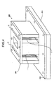
- Fig. 4 is a perspective of a conductive contact unit that stores the conductive contact 1 having the structure described above.
- a conductive contact unit 200 shown in the figure stores a plurality of the conductive contacts 1 and establishes electric connection between a circuit configuration of a semiconductor integrated circuit or the like, which is an inspection object of electric characteristic inspection, and an inspection apparatus.
- the conductive contact unit 200 includes a first plate 201 and a second plate 202 that are provided near both ends of the respective conductive contacts 1 and stores and holds the respective conductive contacts 1.
- the conductive contacts 1 are regularly disposed between these two plates.
- a conductive contact group G is configured by arranging the conductive contacts 1 in one row. However, this is only an example and an arrangement pattern of the conductive contact group G is decided according to an arrangement pattern of electrodes for connection (connection terminals) of the circuit configuration of the inspection object.
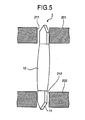
- Fig. 5 is a diagram of a state in a process of storing and attaching the conductive contact 1 according to the first embodiment in the conductive contact unit 200 (for convenience of illustration, the longitudinal direction of the conductive contact 1 is shown short compared with the same in Fig. 4 ).
- a distal end of the conductive contact 1 projecting from a hole 211 of the first plate 201 located in an upper part in Figs. 4 and 5 comes into contact with the electrode for connection provided in the circuit configuration of the inspection object.
- other distal end of the conductive contact 1 projecting from a hole 212 of the second plate 202 located in a lower part in Figs. 4 and 5 comes into contact with an electrode of a circuit board 301 of the inspection apparatus.
- the conductive contact unit 200 When electric characteristic inspection is carried out by using the conductive contact unit 200, usually, the conductive contact unit 200 is vertically reversed from that shown in Fig. 4 . In the drawings described below, for convenience of explanation, a vertical positional relation same as that shown in Fig. 4 is kept.
- the hole 211 of the first plate 201 and the hole 212 of the second plate 202 are formed in columnar shapes through which the conductive contact 1 can be inserted and that have the same diameter.
- the cross-section in the longitudinal direction of the conductive contact 1 is formed in the shape having anisotropy as described above. Therefore, the conductive contact starts to bend in a direction in which a cross-section modulus is small, i.e., a direction perpendicular to long sides of a rectangle, which is a cross-sectional shape of the main body section 11, (a direction in which the plate thickness is small).
- Fig. 6 is a diagram of an attachment state of the conductive contact 1 after offset.
- the conductive contact 1 is in a state in which the conductive contact 1 is bent to bring the surface of the main body section 11 on the long side into contact with the ends of the holes 211 and 212.
- a distal end section of the main body section 11 projecting from the hole 211 of the first plate 201 comes into contact with an electrode for connection 402 of a semiconductor integrated circuit 401 of the inspection object.
- a distal end section of the main body section 11 stored in the hole 212 of the second plate 202 comes into contact with an electrode 302 of the circuit board 301.
- Fig. 7 is a diagram of states of distal ends of the conductive contacts 1 before and after offset and is equivalent to a top view of (a part of) the holes 211 forming the conductive contact group G viewed from an upper surface of the conductive contact unit 200.
- a state I see Fig. 5
- a state II see Fig. 6
- the distal end sections of the conductive contacts 1 projecting from the respective holes 211 are directed to an aligned direction.
- cross-sections perpendicular to longitudinal directions of main body sections are isotropic. Therefore, even if plates are offset in the same manner, it is difficult to uniformalize bending states of all the wire probes.
- the cross-sections perpendicular to the longitudinal directions of the main body sections are non-isotropic and have anisotropy. Therefore, it is possible to uniformalize bending states simply by offsetting the conductive contacts as described above.
- the conductive contact 1 is manufactured by forming the main body section 11 using machining technologies such as plating, etching (including wet etching and dry etching), electrocasting, lithography (including X-ray lithography and ultraviolet lithography),and electric discharge machining (including wire electric discharge machining) and, then, forming the insulating layer 12 on the surface of the main body section 11 with a technology such as coating (including calendaring, extrusion, immersion, spray, spread, and electrodeposition).
- the insulating layer 12 can be formed by using machining technologies such as chemical vapor deposition (CVD), sputtering, and plating.
- metal excellent in abrasion resistance such as iron (Fe), nickel (Ni), and tungsten (W) can be applied.
- insulating layer 12 insulating members of polyurethane, poly-para-xylylene, and the like can be applied. Moreover, insulating films formed of oxide films of alumite and the like can be used as the insulating layer 12.
- the conductive contacts according to the first embodiment are attached to the conductive contact unit to perform electric characteristic inspection, loads on electrodes of the respective conductive contacts are uniformalized. Therefore, it is possible to uniformalize contact resistances in respective contact sections and it is possible to realize more highly accurate and reliable electric characteristic inspection.
- the insulating layer that covers the surface of the area including a section near the center in the longitudinal direction of the main body section and not including both the ends of the main body section, it is possible to prevent electric short-circuit of conductive contacts adjacent to each other when a plurality of conductive contacts are attached to the conductive contact unit and prevent damages and the like due to contact of the conductive contacts.
- the structure of the plate of the conductive contact unit that holds the conductive contact can be simple (see Figs. 5 and 6 ). Therefore, design is easy and cost is low.
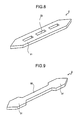
- Fig. 8 is a perspective view of the structure of a main body section of a conductive contact according to a first modification of the first embodiment.
- a conductive contact 2 shown in the figure three through holes 22 having the same shape are formed in a main body section 21 formed in a flat shape and having both ends sharpened in a V shape.
- the through holes 22 are through holes for adjusting a spring constant of the conductive contact 2.
- the number, a shape, and a setting position of the through holes 22 are not limited to those shown in Fig. 2 .
- FIG. 9 is a perspective view of the structure of a main body section of a conductive contact according to a second modification of the first embodiment.
- a conductive contact 3 shown in the figure has two ends 31 having sharpened ends of a V shape and a body section 32 placed between the two ends 31.
- the conductive contact 3 formed in such a shape is obtained by cutting out a section near the center of the main body section 11 of the conductive contact 1 described above.
- the body section 32 in a narrowed shape compared with the other sections, it is possible to give a spring constant different from that of the main body section 11 of the conductive contact 1 to the body section 32.
- the shape (width, length, etc.) of the body section 32 can be changed as appropriate.
- Fig. 10 is a perspective view of a conductive contact according to a third modification of the first embodiment.
- ends 41 are formed in a substantially elliptical circular truncated cone shape and, on the other hand, a body section 42 is formed in a flat shape.
- the conductive contact 4 having such a shape can be molded by applying press work to the conventional wire probe (see the conductive contact 501 shown in Fig. 24 ). Therefore, it is possible to hold down manufacturing cost particularly low.
- Fig. 11 is a perspective view of a conductive contact according to a fourth modification of the first embodiment.
- a conductive contact 5 shown in the figure a flat body section 52 is formed by applying press work to the center section excluding both the ends of the conventional wire probe.
- ends 51 at both sides have sharpened ends and, on the other hand, the body section 51 has anisotropy. Therefore, a bending direction is easily controlled in this structure.
- the conductive contact 5 can be manufactured by using the conventional wire probe. Therefore, like the conductive contact 4, it is possible to hold down manufacturing cost low.
- an insulating layer can be formed near the center of the conductive contacts 2 to 5 explained above.
- Figs. 12 to 14 are partial perspective views of modifications of the shape of the distal end of the conductive contact according to the first embodiment.
- the modifications are equivalent to distal ends formed by machining the distal end of the main body section 11 of the conductive contact 1.
- a distal end 111 shown in Fig. 12 is formed by machining the distal end of the main body section 11 more sharply.
- a distal end 112 shown in Fig. 13 is formed by chamfering a V-shaped curved surface of the distal end of the main body section of the conductive contact 1.
- the distal end 113 shown in Fig. 14 is sharpened in a needle shape.
- optimum shapes only have to be selected according to the circuit structure of an inspection object, the structure of a circuit board of an inspection apparatus.
- the shape of both the ends of the conductive contact can be formed different.
- the distal ends 111 to 113 described above can be formed by applying technologies such as electric discharge machining (including wire electric discharge machining), cutting, turning, and grinding.
- FIG. 15 is a perspective view of a conductive contact according to a second embodiment of the present invention.
- a conductive contact 6 shown in the figure includes a main body section 61 formed in a flat shape and having both ends sharpened in a V shape and a stacked section 62 stacked near the center of the main body section 61 and formed in a rectangular parallelepiped shape having a volume smaller than that of the main body section 61.
- a horizontal cross-section perpendicular to a longitudinal direction of the main body section 61 has anisotropy. Therefore, if a plurality of the conductive contacts 6 are attached to the conductive contact unit 200 and offset as in the first embodiment, it is possible to uniformly align a bending direction of the conductive contacts 6.
- the main body section 61 and the stacked section 62 are formed of different kinds of metal.
- metal such as iron (Fe), nickel (Ni), or tungsten (W) excellent in abrasion resistance is used for the main body section 61 and, on the other hand, metal such as copper (Cu), silver (Ag), gold (Au), or palladium (Pd) having low electric resistance'is used for the stacked section 62.
- Cu copper
- Ag silver
- Au gold
- Pd palladium
- the conductive contact 6 As elements affecting characteristics of the conductive contact, besides the abrasion resistance and the electric resistance, there are stiffness (rigidity), corrosion resistance, low contact resistance, inductance, and the like. Therefore, in forming the conductive contact 6, kinds of metal capable of realizing characteristics that should be given to the conductive contact 6 only have to be combined and stacked. In this sense, the number of kinds of metal that are stacked to form the conductive contact does not have to be two and can be three or more.
- the main body section 61 and the stacked section 62 only have to be stacked by applying the machining technologies such as plating, etching (including wet etching and dry etching), electrocasting, lithography (including X-ray lithography and ultraviolet lithography),and electric discharge machining (including wire electric discharge machining).
- machining technologies such as plating, etching (including wet etching and dry etching), electrocasting, lithography (including X-ray lithography and ultraviolet lithography),and electric discharge machining (including wire electric discharge machining).
- an insulating layer to cover the peripheries of the main body section 61 and the stacked section 62 of the conductive contact 6.
- a method same as that explained in the first embodiment only has to be applied.
- the second embodiment by stacking kinds of meal different from that forming the main body section on the main body section, it is possible to easily give various characteristics to the conductive contact.
- the insulating layer that covers the surface of the area including a section near the center in the longitudinal direction of the main body section and not including both the ends of the main body section, it is possible to prevent electric short-circuit of conductive contacts adjacent to each other when a plurality of conductive contacts are attached to the conductive contact unit and prevent damages and the like due to contact of the conductive contacts,
- Fig. 16 is a perspective view of a conductive contact according to a first modification of the second embodiment.
- a conductive contact 7 shown in the figure a stacked section 72 formed in a shape with distal ends in a longitudinal direction sharpened unlike the stacked section 62 is stacked on a main body section 71 formed in a shape same as that of the main body section 61 of the conductive contact 6.
- Fig. 17 is a perspective view of a conductive contact according to a second modification of the second embodiment.
- a conductive contact 8 shown in the figure a main body section 81 and a stacked section 82 having the same surface area are stacked.
- the main body section 81 has larger thickness (plate thickness) in a stacking direction.
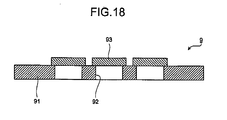
- Fig. 18 is a cross-sectional view of a conductive contact according to a third modification of the second embodiment.
- a conductive contact 9 shown in the figure three through holes 92 are formed in a flat main body section 91 and three stacked sections 93 are stacked to cover opening surfaces on one side of the through holes 92, respectively.
- the stacked sections 93 can be further stacked on opening surfaces on the other side or can be stacked only in a part of the through holes 92.
- the stacked section can be formed of a material other than metal. For example, if resin, resin paint, or the like is stacked on one side or both sides in the structure shown in Fig. 17 , actions and effects same as those obtained by coating the insulating layer are obtained. Even when resin is stacked only on one side, because the conductive contacts 8 have anisotropy, bending directions of the conductive contacts 8 are uniformly aligned and the conductive contacts 8 adjacent to each other do not cause short-circuit.
- a third embodiment of the present invention provides a method of manufacturing a conductive contact suitable in simultaneously manufacturing a large number of conductive contacts including main body sections, horizontal cross-sections of which orthogonal to longitudinal directions have anisotropy, and insulating layers that cover the centers of the main body sections.
- a main body section group including main bodies of a plurality of conductive contacts is molded by applying machining technologies plating, etching (including wet etching and dry etching), electrocasting, lithography (including X-ray lithography and ultraviolet lithography), and electric discharge machining (including wire electric discharge machining) (a molding step).
- Fig. 19 is a diagram of the structure of a main body section group molded by this molding step.
- Fig. 20 is a partially enlarged perspective view of main body sections adjacent to each other in the main body section group.
- a main body section group 100 is formed by coupling a plurality of main body sections 101 formed in a flat shape and having both ends sharpened in a V shape.
- narrowed sections 102 cut out in a direction orthogonal to longitudinal directions of the main body sections 101 are formed.
- Coupling section's 103 that couple the main body sections 101 adjacent to each other are formed on sides 102a of the narrowed sections 102.
- the main body sections 101 formed at farthest ends are coupled to a holding frame section 104 that holds the series of main body sections 101 via the coupling sections 103.
- the holding frame section 104 holds the main body sections 101 such that the longitudinal directions of the respective main body sections 101 are parallel to one another and distal end positions of ends corresponding to the respective main body sections 101 are arranged on one straight line. In this sense, it can be said that the respective main body sections 101 are in a translational symmetry positional relation with respect to a direction in which the main body sections 101 are coupled to the main body sections 101 adjacent thereto (a vertical direction in Fig. 19 ).
- An area of a cross-section (a horizontal cross-section) perpendicular to a longitudinal direction of the coupling section 103 that couples the narrowed sections 102 adjacent to each other has to be smaller than an area of cross-sections perpendicular to the longitudinal directions of the main body sections 101 in the narrowed sections 102. This makes it possible to easily remove the respective main body sections 101 from the main body section group 100 without hurting the main body sections 101.
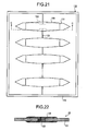
- Fig. 21 is a diagram of the structure of the main body section group after the insulating layer forming step is performed.
- Fig. 22 is a cross-sectional view taken along line C-C in Fig. 21 . As shown in Figs. 21 and 22 , gaps between the narrowed sections 102 and the coupling sections 103 are filled with insulating layers 105.
- the conductive contacts 10 on which the insulating layers 105 are formed, respectively, are removed from the main body section group 100 (a removing step).
- the conductive contacts 10 are rotated with a longitudinal direction center axis of the coupling sections 103 as a rotation center to be removed from the main body section group 100.
- the coupling sections 103 have the area of the horizontal cross-sections smaller than that of the main body sections 101. Therefore, when the conductive contacts 10 are rotated as described above, the coupling sections 103 are disengaged from the sides 102a of the narrowed sections 102 by an action of the rotation. Therefore, it is possible to remove the conductive contacts 10 alone from the holding frame section 104. In removing the conductive contacts 10, the coupling sections 103 are broken near boundaries with the narrowed sections 102. Therefore, it is possible to easily pull out the remains of the coupling sections 103 from the surfaces of the insulating layers 105 and dispose of the remains.
- the main body sections of the conductive contacts are uniformly arranged and molded via the coupling sections, unevenness does not occur in the insulating layers formed in the respective main body sections. Therefore, it is possible to simultaneously manufacture a large number of conductive contacts formed in a uniform shape and realize improvement of productivity.
- the sections where the coupling sections are removed from the insulating layers become cavities.
- the surfaces having conductivity are located on further inside in sufficient depth of the insulating layers than the surfaces of the insulating layers. Therefore, it is not likely that short-circuit is caused among the conductive contacts attached to the conductive contact unit.
- the conductive contact manufactured by the method of manufacturing a conductive contact according to the third embodiment has anisotropy in the shape of the cross-section perpendicular to the longitudinal direction of the main body section as in the first and second embodiments. Therefore, it is possible to easily control a direction in which the conductive contact bends when an external force is applied thereto.
- loads on electrodes of the respective conductive contacts are uniformalized. Therefore, it is possible to uniformalize contact resistances in respective contact sections and realize more highly accurate and reliable electric characteristic inspection.
- the insulating layer that covers the surface of the area including a section near the center in the longitudinal direction of the main body section and not including both the ends of the main body section, it is possible to prevent electric short-circuit of conductive contacts adjacent to each other when a plurality of conductive contacts are attached to the conductive contact unit and prevent damages and the like due to contact of the conductive contacts.
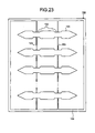
- FIG. 23 is a diagram of another example of the structure of the main body section group.
- a main body section 151 coupled to a main body section group 150 shown in the figure includes two narrowed sections 152 along a longitudinal direction.
- Coupling sections 153 are coupled to the respective narrowed sections 152 as in the case of the narrowed sections 102 described above.
- a plurality of the main body sections 151 are held by a holding frame section 154 while forming a translational symmetry positional relation with one another. Therefore, in the case shown in Fig. 23 , the main body sections 151 adjacent to each other are coupled via two coupling sections 153.
- the present invention is suitable as means for establishing, in performing electric characteristic inspection for a circuit configuration including a plurality of connection terminals, electric connection between the circuit configuration and an inspection apparatus.
Landscapes
- Physics & Mathematics (AREA)
- General Physics & Mathematics (AREA)
- Geometry (AREA)
- Measuring Leads Or Probes (AREA)
- Testing Or Measuring Of Semiconductors Or The Like (AREA)
Abstract
Description
- The present invention relates to a conductive contact that establishes electric connection with a circuit configuration including a plurality of connection terminals by being in physical contact with the connection terminals, and a method of manufacturing such a conductive contact.
- Conductive contacts are employed in performing electric characteristic inspection of a circuit configuration including a plurality of connection terminals. Specifically, these conductive contacts are made to come in physical contact with the connection terminals of the inspection apparatus to establish electric connection with the connection terminals. Wire probe conductive contacts having a circular cross-section are known as such conductive contacts. When a plurality of conductive contacts of the wire probe type are attached to a conductive contact unit, various contrivances are made to align directions in which the conductive contacts bend when an external force acts on main bodies of the conductive contacts (see, for example,
Patent Documents 1 to 3). In these conventional technologies, the bending directions of the conductive contacts are aligned by shifting both ends of each of the conductive elements in a lateral direction by a predetermined distance. -
Fig. 24 is a diagram of another example of attachment of the conventional conductive contact to the conductive contact unit.Fig, 25 is an enlarged diagram of the structure near the conductive contact that is in contact with an inspection apparatus. In aconductive contact 501 shown in these figures, aninsulating layer 512 is formed in amain body section 511 of theconductive contact 501 excluding the ends in a longitudinal direction thereof. Themain body section 511 has a circular cross-section. - A conductive contact unit that stores and holds the
conductive contact 501 having the structure described above includes a two-layerfirst plate 600 on a side (an upper side inFig. 24 ) toward which a circuit configuration for inspecting an inspection object is connected, and includes a three-layersecond plate 700 on a side (a lower side inFig. 24 ) toward which the inspection apparatus is connected. The two-layerfirst plate 600 includes anupper layer plate 601 and alower layer plate 602, while the three-layersecond plate 700 includes anupper layer plate 701, anintermediate layer plate 702, and alower layer plate 703. Anelectrode 802 of acircuit board 801 of the inspection apparatus is in contact with a bottom surface of thelower layer plate 703, and one end of the attachedconductive contact 501 is in contact with theelectrode 802. - The
upper layer plate 601 of thefirst plate 600 has a hole of a diameter larger than the diameter of themain body section 511 and smaller than the diameter of a section covered with aninsulating layer 512. Thelower layer plate 602 of thefirst plate 600 has a hole into which the section covered with theinsulating layer 512 can enter. These two holes are stacked to be vertically coaxial. - In the
second plate 700, ahole 711 of theupper layer plate 701 and ahole 712 of theintermediate layer plate 702 have the same diameter (R2). Both the main body section 511 (diameter r1) and the section covered with the insulating layer 512 (diameter r2) can enter into theholes hole 713 of thelower layer plate 703 has a diameter (R1) smaller than that of the hole of theupper layer plate 701. In other words, only the ends of themain body section 511 can be inserted through thehole 713. That is, the four diameters r1, r2, R1, and R2 are in a relation r1<R1<r2<R2. - The three plates of the
second plate 700 are arranged such that the center axes of their holes are shifted by very small distances'from one another. Consequently, these plates exert force on the attachedconductive contact 501 to bend the attachedconductive contact 501 in a predetermined direction. - Patent Document 1: Japanese Patent Application Laid-open No.
2001-337109
Patent Document 2: Japanese Patent Application Laid-open No.H11-248747
Patent Document 3: Japanese Patent Application Laid-open No.2001-50982 - As described above, the conventional conductive contact has a circular cross-section. Therefore, for example, as shown in
Fig. 6 of Patent Document 3, the upper plate and the lower plate are shifted from each other to shift the center axes of the holes and align a bending direction of the conductive contact. However, actually, the alignment of the bending direction is still insufficient. Therefore, as described above, the holes of the two plates through which both the ends are inserted are shifted to force to control the bending direction of the conductive contact (seeFig. 24 ). However, in the structure shown inFig. 24 , because machining for shifting the center axes of the holes provided in the respective plates is performed, design of hole machining positions becomes complicated and the designing process takes time. Because certain amount of machining error generally exists in machining the plate holes, it is uncertain whether the holes actually shift stepwise when the plates are stacked. Therefore, in the conventional conductive contact unit, it is difficult to uniformalize loads on electrodes of circuit boards of respective conductive contacts and uniformalize contact resistances in respective contact sections. It is likely that a problem occurs in accuracy of electric characteristic inspection itself. - The present invention has been devised in view of the above and it is an object of the present invention to provide a conductive contact in which it is possible to easily control a direction in which a conductive contact bends when an external force is applied thereto and realize more highly accurate and reliable electric characteristic inspection, and a method of manufacturing such a conductive contact.
- To solve the above problems and to achieve the above object, the invention disclosed in
claim 1 is a a conductive contact that establishes electric connection with a circuit configuration including a plurality of connection terminals by being in physical contact with any one of the connection terminals, wherein a shape of a cross-section perpendicular to a longitudinal direction of a main body section of the conductive contact is anisotropic. - In the invention disclosed in
claim 2, in view of the invention disclosed inclaim 1, the cross-section perpendicular to the longitudinal direction of the main body section has a shape symmetrical to each of two axes that pass through the cross-section and are orthogonal to each other. - The invention disclosed in claim 3, in view of the invention disclosed in
claim 1, further includes a stacked section stacked on the main body section and formed of a material different from that of the main body section. - The invention disclosed in claim 4, in view of the invention disclosed in one of
claims 1 to 3, further includes an insulating layer that covers a surface of an area including a section near a center in the longitudinal direction of the main body section and not including both ends of the main body section. - In the invention disclosed in
claim 5, in view of the invention disclosed in one ofclaims 1 to 3, one or a plurality of through holes are provided in the main body section. - In the invention disclosed in
claim 6, in view of the invention disclosed in one ofclaims 1 to 3, at least one end of ends in the longitudinal direction of the main body section is sharp. - In the invention disclosed in claim 7, in view of the invention disclosed in one of
claims 1 to 3, the conductive contact has a narrowed section formed by cutting out a part of sides in the longitudinal direction of the main body section. - In the invention disclosed in claim 8, in view of the invention disclosed in claim 7, the narrowed section is provided near a center in the longitudinal direction of the main body section.
- The invention disclosed in claim 9 is a method of manufacturing a conductive contact that establishes electric connection with a circuit configuration including a plurality of connection terminals by being in physical contact with any one of the connection terminals, the method comprising molding a main body group in which main body sections of a plurality of conductive contacts formed in a same shape by using metal are coupled while forming a translational symmetry positional relation with one another; and forming an insulating layer on a surface of an area including a section near a center in a longitudinal direction of each of the main body sections included in the main body section group molded in the molding and not including both ends of each of the main body sections, wherein in each of the main body sections of the conductive contacts molded in the molding, a shape of a cross-section perpendicular to a longitudinal direction is anisotropic, the main body section includes a narrowed section formed by cutting out a part of sides in the longitudinal direction, and narrowed sections of the main body sections adjacent to each other are coupled.
- In the invention disclosed in
claim 10, in view of the invention disclosed in claim 9, an area of a cross-section perpendicular to a longitudinal direction of a coupling section that couples the narrowed sections adjacent to each other is smaller than an area of the cross-section perpendicular to the longitudinal direction of the main body section in the narrowed section. - The invention disclosed in
claim 11, in view of the invention disclosed inclaim 10, further includes rotating the coupling section coupled to each of the conductive contacts on which the insulating layer is formed in the forming and removing each of the conductive contacts from the main body section group. - According to a conductive contact and a method of manufacturing the conductive contact according to the present invention, because the shape of a section perpendicular to a longitudinal direction of a main body section of the conductive contact is made anisotropic, it is possible to easily control a direction in which the conductive contact bends when an external force is applied thereto and realize more highly accurate and reliable electric characteristic inspection.
-
- [
Fig. 1] Fig. 1 is a perspective view of a conductive contact according to a first embodiment of the present invention. - [
Fig. 2] Fig. 2 is a top view from the direction of an arrow A shown inFig. 1 . - [
Fig. 3] Fig. 3 is a cross-sectional view taken along line B-B inFig. 2 . - [
Fig. 4] Fig. 4 is a perspective view of a conductive contact unit that stores the conductive contact according to the first embodiment of the present invention. - [
Fig. 5] Fig. 5 is a diagram of a state before the conductive contact according to the first embodiment of the present invention is attached to the conductive contact unit and offset. - [
Fig. 6] Fig. 6 is a diagram of a state after the conductive contact according to the first embodiment of the present invention is attached to the conductive contact unit and offset. - [
Fig. 7] Fig. 7 is a diagram of states of respective distal ends of a conductive contact group before and after offset. - [
Fig. 8] Fig. 8 is a perspective view of a conductive contact according to a first modification of the first embodiment of the present invention. - [
Fig. 9] Fig. 9 is a perspective view of a conductive contact according to a second modification of the first embodiment of the present invention. - [
Fig. 10] Fig. 10 is a perspective view of a conductive contact according to a third modification of the first embodiment of the present invention. - [
Fig. 11] Fig. 11 is a perspective view of a conductive contact according to a fourth modification of the first embodiment of the present invention. - [
Fig. 12] Fig. 12 is a perspective view of a modification (a first example) of the shape of a distal end of the conductive contact according to the first embodiment of the present invention. - [
Fig. 13] Fig. 13 is a perspective view of a modification (a second example) of the shape of the distal end of the conductive contact according to the first embodiment of the present invention. - [
Fig. 14] Fig. 14 is a perspective view of a modification (a third example) of the shape of the distal end of the conductive contact according to the first embodiment of the present invention. - [
Fig. 15] Fig. 15 is a perspective view of a conductive contact according to a second embodiment of the present invention. - [
Fig. 16] Fig. 16 is a perspective view of a conductive contact according to a first modification of the second embodiment of the present invention. - [
Fig. 17] Fig. 17 is a perspective view of a conductive contact according to a second modification of the second embodiment of the present invention. - [
Fig. 18] Fig. 18 is a cross-sectional view of a conductive contact according to a third modification of the second embodiment of the present invention. - [
Fig. 19] Fig. 19 is a diagram of the structure of a main body section group molded in a molding step of a method of manufacturing a conductive contact according to a third embodiment of the present invention. - [
Fig. 20] Fig. 20 is a partially enlarged perspective view of main body sections adjacent to each other in the main body section group. - [
Fig. 21] Fig. 21 is a diagram of the structure of a main body section group after an insulating layer forming step of the method of manufacturing a conductive contact according to the third embodiment of the present invention. [Fig. 22] Fig. 22 is a cross-sectional view taken along line C-C inFig. 21 . - [
Fig. 23] Fig. 23 is a diagram of another example of the structure of the main body section group. - [
Fig. 24] Fig. 24 is a diagram of an example of attachment of a conventional conductive contact to a conductive contact unit. - [
Fig. 25] Fig. 25 is a partially enlarged view of the attachment structure of the conductive contact that is in contact with an inspection apparatus side. - 1, 2, 3, 4, 5, 6, 7, 8, 9, 10, 501 Conductive contacts
11, 21, 61, 71, 81, 91, 101, 151, 511Main body sections
22, 92 Through holes
31, 41, 51 Ends
32, 42, 52 Body sections
62, 72, 82, 93 Stacked sections
100, 150 Main body section groups
102, 152 Narrowed sections
102a Side
103, 153 Coupling sections
104, 154 Holding frame sections
111, 112, 113 Distal ends
200 Conductive contact unit
201, 600 First plates
202, 700 Second plates
211, 212, 711; 712, 713 Holes
301, 801 Circuit boards
302, 802 Electrodes
401 Semiconductor integrated circuit
402 Electrode for connection
601, 701 Upper layer plates
602, 703 Lower layer plates
702 Intermediate layer plate
G Conductive contact group - Best modes for carrying out the present invention (hereinafter referred to as "embodiments") are explained below with reference to the accompanying drawings. It should be noted that the drawings are schematic and a relation between thicknesses and widths of respective sections, a ratio of thicknesses of the respective sections, and the like can be different from realistic ones. It goes without saying that sections having different relations and ratios of dimensions among the drawings can be included.
-
Fig. 1 is a perspective view of a conductive contact according to a first embodiment of the present invention.Fig. 2 is a top view from the direction of an arrow A shown inFig. 1. Fig. 3 is a cross-sectional view taken along line B-B inFig. 2 . Aconductive contact 1 shown in these figures is a wire probe and includes amain body section 11 formed in a flat shape and having both ends sharpened in a V shape at both ends and an insulatinglayer 12 formed to cover the surface of themain body section 11 near the center excluding both the ends of thismain body section 11. A cross-section (a horizontal cross-section) in a direction perpendicular to a longitudinal direction of themain body section 11 is rectangular in cross-section as-shown inFig. 3 as well. On the other hand, the entireconductive contact 1 including the insulatinglayer 12 is substantially elliptical in cross-section. Thus, in theconductive contact 1, a cross-sectional shape in the direction perpendicular to the longitudinal direction'of themain body section 11 is anisotropic. In particular, in the first embodiment, theconductive contact 1 is formed in a shape symmetrical to each of two axes that pass the cross-section and are orthogonal to each other. -
Fig. 4 is a perspective of a conductive contact unit that stores theconductive contact 1 having the structure described above. Aconductive contact unit 200 shown in the figure stores a plurality of theconductive contacts 1 and establishes electric connection between a circuit configuration of a semiconductor integrated circuit or the like, which is an inspection object of electric characteristic inspection, and an inspection apparatus. Theconductive contact unit 200 includes afirst plate 201 and asecond plate 202 that are provided near both ends of the respectiveconductive contacts 1 and stores and holds the respectiveconductive contacts 1. Theconductive contacts 1 are regularly disposed between these two plates. In the case shown inFig. 4 , a conductive contact group G is configured by arranging theconductive contacts 1 in one row. However, this is only an example and an arrangement pattern of the conductive contact group G is decided according to an arrangement pattern of electrodes for connection (connection terminals) of the circuit configuration of the inspection object. -
Fig. 5 is a diagram of a state in a process of storing and attaching theconductive contact 1 according to the first embodiment in the conductive contact unit 200 (for convenience of illustration, the longitudinal direction of theconductive contact 1 is shown short compared with the same inFig. 4 ). A distal end of theconductive contact 1 projecting from ahole 211 of thefirst plate 201 located in an upper part inFigs. 4 and5 comes into contact with the electrode for connection provided in the circuit configuration of the inspection object. On the other hand, other distal end of theconductive contact 1 projecting from ahole 212 of thesecond plate 202 located in a lower part inFigs. 4 and5 comes into contact with an electrode of acircuit board 301 of the inspection apparatus. When electric characteristic inspection is carried out by using theconductive contact unit 200, usually, theconductive contact unit 200 is vertically reversed from that shown inFig. 4 . In the drawings described below, for convenience of explanation, a vertical positional relation same as that shown inFig. 4 is kept. - The
hole 211 of thefirst plate 201 and thehole 212 of thesecond plate 202 are formed in columnar shapes through which theconductive contact 1 can be inserted and that have the same diameter. When theconductive contact 1 is attached to theconductive contact unit 200, from a state shown inFig. 5 , any one of thefirst plate 201 and thesecond plate 202 is moved in a horizontal direction in the figure with respect to the other plate (this operation is hereinafter referred to as "offset"), whereby center axes of theholes Fig. 5 are shifted. As a result, theconductive contact 1 is subjected to an external force and starts to bend. The cross-section in the longitudinal direction of theconductive contact 1 is formed in the shape having anisotropy as described above. Therefore, the conductive contact starts to bend in a direction in which a cross-section modulus is small, i.e., a direction perpendicular to long sides of a rectangle, which is a cross-sectional shape of themain body section 11, (a direction in which the plate thickness is small). -
Fig. 6 is a diagram of an attachment state of theconductive contact 1 after offset. As shown in this figure, theconductive contact 1 is in a state in which theconductive contact 1 is bent to bring the surface of themain body section 11 on the long side into contact with the ends of theholes main body section 11 projecting from thehole 211 of thefirst plate 201 comes into contact with an electrode forconnection 402 of a semiconductor integratedcircuit 401 of the inspection object. On the other hand, a distal end section of themain body section 11 stored in thehole 212 of thesecond plate 202 comes into contact with anelectrode 302 of thecircuit board 301. -
Fig. 7 is a diagram of states of distal ends of theconductive contacts 1 before and after offset and is equivalent to a top view of (a part of) theholes 211 forming the conductive contact group G viewed from an upper surface of theconductive contact unit 200. As shown inFig. 7 , in a state I (seeFig. 5 ) before offset in which center axes of theholes conductive contacts 1 are directed to random directions. On the other hand, in a state II (seeFig. 6 ) after offset because the respectiveconductive contacts 1 bend in the same manner, the distal end sections of theconductive contacts 1 projecting from therespective holes 211 are directed to an aligned direction. - In the case of the conventional wire probes having the circular cross-sectional shape, cross-sections perpendicular to longitudinal directions of main body sections are isotropic. Therefore, even if plates are offset in the same manner, it is difficult to uniformalize bending states of all the wire probes. On the other hand, in conductive contacts according to the first embodiment, the cross-sections perpendicular to the longitudinal directions of the main body sections are non-isotropic and have anisotropy. Therefore, it is possible to uniformalize bending states simply by offsetting the conductive contacts as described above.
- A method of manufacturing the
conductive contact 1 is explained. Theconductive contact 1 is manufactured by forming themain body section 11 using machining technologies such as plating, etching (including wet etching and dry etching), electrocasting, lithography (including X-ray lithography and ultraviolet lithography),and electric discharge machining (including wire electric discharge machining) and, then, forming the insulatinglayer 12 on the surface of themain body section 11 with a technology such as coating (including calendaring, extrusion, immersion, spray, spread, and electrodeposition). The insulatinglayer 12 can be formed by using machining technologies such as chemical vapor deposition (CVD), sputtering, and plating. - As metal forming the main
body section portion 11, metal excellent in abrasion resistance such as iron (Fe), nickel (Ni), and tungsten (W) can be applied. As the insulatinglayer 12, insulating members of polyurethane, poly-para-xylylene, and the like can be applied. Moreover, insulating films formed of oxide films of alumite and the like can be used as the insulatinglayer 12. - According to the first embodiment of the present invention explained above, by giving anisotropy to the shape of the cross-section perpendicular to the longitudinal direction of the main body section of the conductive contact, it is possible to easily control a direction in which the conductive contact bends when an external force is applied thereto. As a result, when the conductive contacts according to the first embodiment are attached to the conductive contact unit to perform electric characteristic inspection, loads on electrodes of the respective conductive contacts are uniformalized. Therefore, it is possible to uniformalize contact resistances in respective contact sections and it is possible to realize more highly accurate and reliable electric characteristic inspection.
- According to the first embodiment, by forming the insulating layer that covers the surface of the area including a section near the center in the longitudinal direction of the main body section and not including both the ends of the main body section, it is possible to prevent electric short-circuit of conductive contacts adjacent to each other when a plurality of conductive contacts are attached to the conductive contact unit and prevent damages and the like due to contact of the conductive contacts.
- Moreover, according to the first embodiment, by giving anisotropy to the shape of the cross-section perpendicular to the longitudinal direction of the main body section of the conductive contact, the structure of the plate of the conductive contact unit that holds the conductive contact can be simple (see
Figs. 5 and6 ). Therefore, design is easy and cost is low. -
Fig. 8 is a perspective view of the structure of a main body section of a conductive contact according to a first modification of the first embodiment. In aconductive contact 2 shown in the figure, three throughholes 22 having the same shape are formed in amain body section 21 formed in a flat shape and having both ends sharpened in a V shape. The through holes 22 are through holes for adjusting a spring constant of theconductive contact 2. The number, a shape, and a setting position of the throughholes 22 are not limited to those shown inFig. 2 . -
Fig. 9 is a perspective view of the structure of a main body section of a conductive contact according to a second modification of the first embodiment. A conductive contact 3 shown in the figure has two ends 31 having sharpened ends of a V shape and abody section 32 placed between the two ends 31. The conductive contact 3 formed in such a shape is obtained by cutting out a section near the center of themain body section 11 of theconductive contact 1 described above. In this case, by forming thebody section 32 in a narrowed shape compared with the other sections, it is possible to give a spring constant different from that of themain body section 11 of theconductive contact 1 to thebody section 32. The shape (width, length, etc.) of thebody section 32 can be changed as appropriate. -
Fig. 10 is a perspective view of a conductive contact according to a third modification of the first embodiment. In a conductive contact 4 shown in the figure, ends 41 are formed in a substantially elliptical circular truncated cone shape and, on the other hand, abody section 42 is formed in a flat shape. The conductive contact 4 having such a shape can be molded by applying press work to the conventional wire probe (see theconductive contact 501 shown inFig. 24 ). Therefore, it is possible to hold down manufacturing cost particularly low. -
Fig. 11 is a perspective view of a conductive contact according to a fourth modification of the first embodiment. In aconductive contact 5 shown in the figure, aflat body section 52 is formed by applying press work to the center section excluding both the ends of the conventional wire probe. As a result, ends 51 at both sides have sharpened ends and, on the other hand, thebody section 51 has anisotropy. Therefore, a bending direction is easily controlled in this structure. In this case, as in the case described above, theconductive contact 5 can be manufactured by using the conventional wire probe. Therefore, like the conductive contact 4, it is possible to hold down manufacturing cost low. - It goes without saying that, as in the
conductive contact 1, an insulating layer can be formed near the center of theconductive contacts 2 to 5 explained above. -
Figs. 12 to 14 are partial perspective views of modifications of the shape of the distal end of the conductive contact according to the first embodiment. The modifications are equivalent to distal ends formed by machining the distal end of themain body section 11 of theconductive contact 1. Among the modifications, adistal end 111 shown inFig. 12 is formed by machining the distal end of themain body section 11 more sharply. Adistal end 112 shown inFig. 13 is formed by chamfering a V-shaped curved surface of the distal end of the main body section of theconductive contact 1. Thedistal end 113 shown inFig. 14 is sharpened in a needle shape. As the shapes of the distal ends shown in the figures, optimum shapes only have to be selected according to the circuit structure of an inspection object, the structure of a circuit board of an inspection apparatus. The shape of both the ends of the conductive contact can be formed different. - The distal ends 111 to 113 described above can be formed by applying technologies such as electric discharge machining (including wire electric discharge machining), cutting, turning, and grinding.
-
Fig. 15 is a perspective view of a conductive contact according to a second embodiment of the present invention. Aconductive contact 6 shown in the figure includes amain body section 61 formed in a flat shape and having both ends sharpened in a V shape and astacked section 62 stacked near the center of themain body section 61 and formed in a rectangular parallelepiped shape having a volume smaller than that of themain body section 61. In theconductive contact 6, as in the first embodiment, a horizontal cross-section perpendicular to a longitudinal direction of themain body section 61 has anisotropy. Therefore, if a plurality of theconductive contacts 6 are attached to theconductive contact unit 200 and offset as in the first embodiment, it is possible to uniformly align a bending direction of theconductive contacts 6. - The
main body section 61 and the stackedsection 62 are formed of different kinds of metal. For example, metal such as iron (Fe), nickel (Ni), or tungsten (W) excellent in abrasion resistance is used for themain body section 61 and, on the other hand, metal such as copper (Cu), silver (Ag), gold (Au), or palladium (Pd) having low electric resistance'is used for the stackedsection 62. This makes it possible to realize a conductive contact excellent in abrasion resistance and an electric resistance characteristic. This is an effect that cannot be obtained when the conductive contact is formed of one kind of metal and is an effect peculiar to the second embodiment. - As elements affecting characteristics of the conductive contact, besides the abrasion resistance and the electric resistance, there are stiffness (rigidity), corrosion resistance, low contact resistance, inductance, and the like. Therefore, in forming the
conductive contact 6, kinds of metal capable of realizing characteristics that should be given to theconductive contact 6 only have to be combined and stacked. In this sense, the number of kinds of metal that are stacked to form the conductive contact does not have to be two and can be three or more. - In manufacturing the
conductive contact 6, as in the first embodiment, themain body section 61 and the stackedsection 62 only have to be stacked by applying the machining technologies such as plating, etching (including wet etching and dry etching), electrocasting, lithography (including X-ray lithography and ultraviolet lithography),and electric discharge machining (including wire electric discharge machining). - In the second embodiment, as in the first embodiment, it is also possible to form an insulating layer to cover the peripheries of the
main body section 61 and the stackedsection 62 of theconductive contact 6. In forming such an insulating layer, a method same as that explained in the first embodiment only has to be applied. - According to the second embodiment of the present invention explained above, by giving anisotropy to the shape of the cross-section perpendicular to the longitudinal direction of the main body section of the conductive contact, it is possible to easily control a direction in which the conductive contact bends when an external force is applied thereto. As a result, when conductive contacts according to the second embodiment are attached to a conductive contact unit to perform electric characteristic inspection, loads on electrodes of the respective conductive contacts are uniformalized. Therefore, it is possible to uniformalize contact resistances in respective contact sections and realize more highly accurate and reliable electric characteristic inspection.
- According to the second embodiment, by stacking kinds of meal different from that forming the main body section on the main body section, it is possible to easily give various characteristics to the conductive contact.
- Moreover, according to the second embodiment, by forming the insulating layer that covers the surface of the area including a section near the center in the longitudinal direction of the main body section and not including both the ends of the main body section, it is possible to prevent electric short-circuit of conductive contacts adjacent to each other when a plurality of conductive contacts are attached to the conductive contact unit and prevent damages and the like due to contact of the conductive contacts,
-
Fig. 16 is a perspective view of a conductive contact according to a first modification of the second embodiment. In a conductive contact 7 shown in the figure, astacked section 72 formed in a shape with distal ends in a longitudinal direction sharpened unlike the stackedsection 62 is stacked on amain body section 71 formed in a shape same as that of themain body section 61 of theconductive contact 6. By changing a shape of the stacked section in this way, it is possible to set characteristics of the conductive contact 7 different from the characteristics of theconductive contact 6. -
Fig. 17 is a perspective view of a conductive contact according to a second modification of the second embodiment. In a conductive contact 8 shown in the figure, amain body section 81 and astacked section 82 having the same surface area are stacked. However, themain body section 81 has larger thickness (plate thickness) in a stacking direction. By changing a ratio of the plate thickness of themain body section 81 and the plate thickness of the stackedsection 82, it is also possible to adjust the characteristics of the conductive contact 8. -
Fig. 18 is a cross-sectional view of a conductive contact according to a third modification of the second embodiment. In a conductive contact 9 shown in the figure, three throughholes 92 are formed in a flatmain body section 91 and threestacked sections 93 are stacked to cover opening surfaces on one side of the throughholes 92, respectively. Thestacked sections 93 can be further stacked on opening surfaces on the other side or can be stacked only in a part of the through holes 92. - It is also possible to form still different modifications by appropriately combining the structures of the
conductive contacts 6 to 9 explained above. In the second embodiment, as in the first embodiment, it is possible to narrow a section near the center of the main body section of the conductive contact (seeFig. 9 ) or apply machining for changing a shape of the distal ends (seeFigs. 12 to 14 ). The stacked section can be formed of a material other than metal. For example, if resin, resin paint, or the like is stacked on one side or both sides in the structure shown inFig. 17 , actions and effects same as those obtained by coating the insulating layer are obtained. Even when resin is stacked only on one side, because the conductive contacts 8 have anisotropy, bending directions of the conductive contacts 8 are uniformly aligned and the conductive contacts 8 adjacent to each other do not cause short-circuit. - A third embodiment of the present invention provides a method of manufacturing a conductive contact suitable in simultaneously manufacturing a large number of conductive contacts including main body sections, horizontal cross-sections of which orthogonal to longitudinal directions have anisotropy, and insulating layers that cover the centers of the main body sections.
- In the method of manufacturing a conductive contact according to the third embodiment, first, a main body section group including main bodies of a plurality of conductive contacts is molded by applying machining technologies plating, etching (including wet etching and dry etching), electrocasting, lithography (including X-ray lithography and ultraviolet lithography), and electric discharge machining (including wire electric discharge machining) (a molding step).
Fig. 19 is a diagram of the structure of a main body section group molded by this molding step.Fig. 20 is a partially enlarged perspective view of main body sections adjacent to each other in the main body section group. As shown in the figures, a mainbody section group 100 is formed by coupling a plurality ofmain body sections 101 formed in a flat shape and having both ends sharpened in a V shape. In the centers of themain body sections 101, narrowedsections 102 cut out in a direction orthogonal to longitudinal directions of themain body sections 101 are formed. Coupling section's 103 that couple themain body sections 101 adjacent to each other are formed on sides 102a of the narrowedsections 102. - The
main body sections 101 formed at farthest ends are coupled to a holdingframe section 104 that holds the series ofmain body sections 101 via thecoupling sections 103. As shown inFig. 19 , the holdingframe section 104 holds themain body sections 101 such that the longitudinal directions of the respectivemain body sections 101 are parallel to one another and distal end positions of ends corresponding to the respectivemain body sections 101 are arranged on one straight line. In this sense, it can be said that the respectivemain body sections 101 are in a translational symmetry positional relation with respect to a direction in which themain body sections 101 are coupled to themain body sections 101 adjacent thereto (a vertical direction inFig. 19 ). - An area of a cross-section (a horizontal cross-section) perpendicular to a longitudinal direction of the
coupling section 103 that couples the narrowedsections 102 adjacent to each other has to be smaller than an area of cross-sections perpendicular to the longitudinal directions of themain body sections 101 in the narrowedsections 102. This makes it possible to easily remove the respectivemain body sections 101 from the mainbody section group 100 without hurting themain body sections 101. - Following the molding step explained above, both the ends of the respective
main body sections 101 are appropriately masked and, then, insulating layers are formed in the centers of themain body sections 101 not masked (an insulating layer forming step). The insulating layers can be formed in the same manner as the insulatinglayer 12 of theconductive contact 1 according to the first embodiment.Fig. 21 is a diagram of the structure of the main body section group after the insulating layer forming step is performed.Fig. 22 is a cross-sectional view taken along line C-C inFig. 21 . As shown inFigs. 21 and 22 , gaps between thenarrowed sections 102 and thecoupling sections 103 are filled with insulatinglayers 105. - Thereafter, the
conductive contacts 10 on which the insulatinglayers 105 are formed, respectively, are removed from the main body section group 100 (a removing step). In this removing step, theconductive contacts 10 are rotated with a longitudinal direction center axis of thecoupling sections 103 as a rotation center to be removed from the mainbody section group 100. As explained about the molding step, thecoupling sections 103 have the area of the horizontal cross-sections smaller than that of themain body sections 101. Therefore, when theconductive contacts 10 are rotated as described above, thecoupling sections 103 are disengaged from the sides 102a of the narrowedsections 102 by an action of the rotation. Therefore, it is possible to remove theconductive contacts 10 alone from the holdingframe section 104. In removing theconductive contacts 10, thecoupling sections 103 are broken near boundaries with the narrowedsections 102. Therefore, it is possible to easily pull out the remains of thecoupling sections 103 from the surfaces of the insulatinglayers 105 and dispose of the remains. - By coupling the
coupling sections 103 to the sides 102a of the narrowedsections 102 of themain body sections 101 in this way, after themain body sections 101 are removed, sections where thecoupling sections 103 are removed become cavities. The cavities are connected to the surfaces of the sides 102a. However, the surfaces are located on further inside in sufficient depth of the insulatinglayers 105 than the surfaces of the insulating layers 105. Therefore, even if the adjacentconductive contacts 10 come into contact with each other when theconductive contacts 10 are attached to theconductive contact unit 200, it is not likely that short-circuit or the like is caused. - According to the third embodiment of the present invention explained above, because the main body sections of the conductive contacts are uniformly arranged and molded via the coupling sections, unevenness does not occur in the insulating layers formed in the respective main body sections. Therefore, it is possible to simultaneously manufacture a large number of conductive contacts formed in a uniform shape and realize improvement of productivity.
- According to the third embodiment, by coupling the coupling sections to the narrowed sections of the main body sections, the sections where the coupling sections are removed from the insulating layers become cavities. The surfaces having conductivity are located on further inside in sufficient depth of the insulating layers than the surfaces of the insulating layers. Therefore, it is not likely that short-circuit is caused among the conductive contacts attached to the conductive contact unit.
- The conductive contact manufactured by the method of manufacturing a conductive contact according to the third embodiment has anisotropy in the shape of the cross-section perpendicular to the longitudinal direction of the main body section as in the first and second embodiments. Therefore, it is possible to easily control a direction in which the conductive contact bends when an external force is applied thereto. As a result, when conductive contacts according to the third embodiment are attached to a conductive contact unit to perform electric characteristic inspection, as in the first and second embodiments, loads on electrodes of the respective conductive contacts are uniformalized. Therefore, it is possible to uniformalize contact resistances in respective contact sections and realize more highly accurate and reliable electric characteristic inspection.
- In the case of the third embodiment, as in the first and second embodiments, by forming the insulating layer that covers the surface of the area including a section near the center in the longitudinal direction of the main body section and not including both the ends of the main body section, it is possible to prevent electric short-circuit of conductive contacts adjacent to each other when a plurality of conductive contacts are attached to the conductive contact unit and prevent damages and the like due to contact of the conductive contacts.
- The structure of the main body section group is not limited to that shown in
Fig. 19 .Fig. 23 is a diagram of another example of the structure of the main body section group. Amain body section 151 coupled to a mainbody section group 150 shown in the figure includes two narrowedsections 152 along a longitudinal direction. Couplingsections 153 are coupled to the respective narrowedsections 152 as in the case of the narrowedsections 102 described above. A plurality of themain body sections 151 are held by a holdingframe section 154 while forming a translational symmetry positional relation with one another. Therefore, in the case shown inFig. 23 , themain body sections 151 adjacent to each other are coupled via twocoupling sections 153. When a conductive contact is manufactured from the mainbody section group 150 having such structure, after an insulating layer is formed in the same manner as described above, thecoupling sections 153 are rotated with respect to themain body section 151 to separate themain body section 151 and thecoupling sections 153. As a result, when all the fourcoupling sections 153 coupled to themain body section 151 are cut off, themain body section 151 is removed from the mainbody section group 150. - The first to third embodiments have been described in detail as the best modes for carrying out the present invention. However, the present invention should not be limited by only the three embodiments. The present invention can include various embodiments and the like not described in this specification. Various design changes and the like can be applied to the present invention within a range not departing from the technical idea specified by patent claims.
- The present invention is suitable as means for establishing, in performing electric characteristic inspection for a circuit configuration including a plurality of connection terminals, electric connection between the circuit configuration and an inspection apparatus.
Claims (11)
- A conductive contact that establishes electric connection with a circuit configuration including a plurality of connection terminals by being in physical contact with any one of the connection terminals, wherein
a shape of a cross-section perpendicular to a longitudinal direction of a main body section of the conductive contact is anisotropic. - The conductive contact according to claim 1, wherein the cross-section perpendicular to the longitudinal direction of the main body section has a shape symmetrical to each of two axes that pass through the cross-section and are orthogonal to each other.
- The conductive contact according to claim 1, further comprising a stacked section stacked on the main body section and formed of a material different from that of the main body section.
- The conductive contact according to any one of claims 1 to 3, further comprising an insulating layer that covers a surface of an area including a section near a center in the longitudinal direction of the main body section and not including both ends of the main body section.
- The conductive contact according to any one of claims 1 to 3, wherein one or a plurality of through holes are provided in the main body section.
- The conductive contact according to any one of claims 1 to 3, wherein at least one end of ends in the longitudinal direction of the main body section is sharpened.
- The conductive contact according to any one of claims 1 to 3, wherein the conductive contact has a narrowed section formed by cutting out a part of sides in the longitudinal direction of the main body section.
- The conductive contact according to claim 7, wherein the narrowed section is provided near a center in the longitudinal direction of the main body section.
- A method of manufacturing a conductive contact that establishes electric connection with a circuit configuration including a plurality of connection terminals by being in physical contact with any one of the connection terminals, the method comprising:a molding step of molding a main body group in which main body sections of a plurality of conductive contacts formed in a same shape by using metal are coupled while forming a translational symmetry positional relation with one another; andan insulating layer forming step of forming an insulating layer on a surface of an area including a section near a center in a longitudinal direction of each of the main body sections included in the main body section group molded in the molding step and not including both ends of each of the main body sections, whereinin each of the main body sections of the conductive contacts molded in the molding step, a shape of a cross-section perpendicular to a longitudinal direction is anisotropic,the main body section includes a narrowed section formed by.cutting out a part of sides in the longitudinal direction, andnarrowed sections of the main body sections adjacent to each other are coupled.
- The method of manufacturing a conductive contact according to claim 9, wherein an area of a cross-section perpendicular to a longitudinal direction of a coupling section that couples the narrowed sections adjacent to each other is smaller than an area of the cross-section perpendicular to the longitudinal direction of the main body section in the narrowed section.
- The method of manufacturing a conductive contact according to claim 10, further comprising a removing step of rotating the coupling section coupled to each of the conductive contacts on which the insulating layer is formed in the insulating layer forming step and removing each of the conductive contacts,from the main body section group.
Applications Claiming Priority (2)
| Application Number | Priority Date | Filing Date | Title |
|---|---|---|---|
| JP2005263036A JP4823617B2 (en) | 2005-09-09 | 2005-09-09 | Conductive contact and method for manufacturing conductive contact |
| PCT/JP2006/317789 WO2007029791A1 (en) | 2005-09-09 | 2006-09-07 | Conductive contact and method for manufacturing conductive contact |
Publications (2)
| Publication Number | Publication Date |
|---|---|
| EP1923708A1 true EP1923708A1 (en) | 2008-05-21 |
| EP1923708A4 EP1923708A4 (en) | 2012-05-09 |
Family
ID=37835906
Family Applications (1)
| Application Number | Title | Priority Date | Filing Date |
|---|---|---|---|
| EP06797646A Withdrawn EP1923708A4 (en) | 2005-09-09 | 2006-09-07 | DRIVER CONTACT AND METHOD OF MANUFACTURING |
Country Status (7)
| Country | Link |
|---|---|
| US (1) | US7956288B2 (en) |
| EP (1) | EP1923708A4 (en) |
| JP (1) | JP4823617B2 (en) |
| KR (1) | KR101012083B1 (en) |
| CN (1) | CN101258409B (en) |
| TW (1) | TWI315791B (en) |
| WO (1) | WO2007029791A1 (en) |
Cited By (4)
| Publication number | Priority date | Publication date | Assignee | Title |
|---|---|---|---|---|
| EP2060921A1 (en) * | 2007-11-16 | 2009-05-20 | Technoprobe S.p.A | Contact probe for testing head having vertical probes and related testing head for testing microstructure electric performance |
| DE102013011968A1 (en) * | 2013-07-18 | 2015-02-19 | Feinmetall Gmbh | Electrical test device for electrical contact contacting of an electrical test specimen |
| EP2117081B1 (en) * | 2008-05-09 | 2018-11-07 | Feinmetall GmbH | Electric contact element |
| WO2019091946A1 (en) * | 2017-11-09 | 2019-05-16 | Technoprobe S.P.A. | Contact probe for a testing head for testing high-frequency devices |
Families Citing this family (35)
| Publication number | Priority date | Publication date | Assignee | Title |
|---|---|---|---|---|
| JP2009014480A (en) * | 2007-07-04 | 2009-01-22 | Koyo Technos:Kk | Inspection tool |
| DE102010048189B4 (en) * | 2010-10-13 | 2012-11-15 | Heraeus Materials Technology Gmbh & Co. Kg | Precious metal-containing contact piece on a spring carrier with rotationally symmetrical bending moment |
| JP2014071069A (en) * | 2012-10-01 | 2014-04-21 | Japan Electronic Materials Corp | Vertical type probe |
| CN104755943B (en) * | 2012-12-04 | 2018-04-27 | 日本电子材料株式会社 | Electrical contact member |
| TWI472772B (en) * | 2013-01-11 | 2015-02-11 | Mpi Corp | Probe, probe card and manufacturing method thereof |
| JP6305754B2 (en) * | 2013-12-20 | 2018-04-04 | 東京特殊電線株式会社 | Contact probe unit |
| JP1529613S (en) * | 2014-12-19 | 2015-07-27 | ||
| JP6832661B2 (en) * | 2016-09-28 | 2021-02-24 | 株式会社日本マイクロニクス | Probe card and contact inspection device |
| JP6813461B2 (en) * | 2017-09-19 | 2021-01-13 | タツタ電線株式会社 | Seat sensor |
| TWI626454B (en) * | 2017-11-20 | 2018-06-11 | Probe device and method of manufacturing same | |
| JP7254450B2 (en) * | 2018-05-16 | 2023-04-10 | 日本電産リード株式会社 | Probe, inspection jig, inspection apparatus, and probe manufacturing method |
| CN112424614B (en) * | 2018-07-18 | 2024-11-05 | 日本电产理德股份有限公司 | Probe, inspection jig, inspection device, and method for manufacturing probe |
| US11973301B2 (en) | 2018-09-26 | 2024-04-30 | Microfabrica Inc. | Probes having improved mechanical and/or electrical properties for making contact between electronic circuit elements and methods for making |
| US12078657B2 (en) | 2019-12-31 | 2024-09-03 | Microfabrica Inc. | Compliant pin probes with extension springs, methods for making, and methods for using |
| US12181493B2 (en) | 2018-10-26 | 2024-12-31 | Microfabrica Inc. | Compliant probes including dual independently operable probe contact elements including at least one flat extension spring, methods for making, and methods for using |
| US12000865B2 (en) | 2019-02-14 | 2024-06-04 | Microfabrica Inc. | Multi-beam vertical probes with independent arms formed of a high conductivity metal for enhancing current carrying capacity and methods for making such probes |
| US11768227B1 (en) | 2019-02-22 | 2023-09-26 | Microfabrica Inc. | Multi-layer probes having longitudinal axes and preferential probe bending axes that lie in planes that are nominally parallel to planes of probe layers |
| IT201900024889A1 (en) * | 2019-12-19 | 2021-06-19 | Technoprobe Spa | Contact probe for high frequency applications with improved current carrying capacity |
| US12196782B2 (en) | 2019-12-31 | 2025-01-14 | Microfabrica Inc. | Probes with planar unbiased spring elements for electronic component contact, methods for making such probes, and methods for using such probes |
| US11867721B1 (en) | 2019-12-31 | 2024-01-09 | Microfabrica Inc. | Probes with multiple springs, methods for making, and methods for using |
| US12196781B2 (en) | 2019-12-31 | 2025-01-14 | Microfabrica Inc. | Probes with planar unbiased spring elements for electronic component contact, methods for making such probes, and methods for using such probes |
| US11761982B1 (en) | 2019-12-31 | 2023-09-19 | Microfabrica Inc. | Probes with planar unbiased spring elements for electronic component contact and methods for making such probes |
| TWI728665B (en) * | 2020-01-21 | 2021-05-21 | 中華精測科技股份有限公司 | Probe card device having directivity probe |
| TWI712802B (en) * | 2020-01-21 | 2020-12-11 | 中華精測科技股份有限公司 | Probe card device and neck-like probe thereof |
| US11774467B1 (en) | 2020-09-01 | 2023-10-03 | Microfabrica Inc. | Method of in situ modulation of structural material properties and/or template shape |
| JP7485945B2 (en) * | 2020-09-08 | 2024-05-17 | 山一電機株式会社 | Kelvin contact for inspection, Kelvin socket for inspection, and method for manufacturing Kelvin contact for inspection |
| US12146898B2 (en) | 2020-10-02 | 2024-11-19 | Microfabrica Inc. | Multi-beam probes with decoupled structural and current carrying beams and methods of making |
| KR102265359B1 (en) * | 2021-01-26 | 2021-06-15 | 주식회사 메디션 | Probe pin using conductive thin film and test socket including the same |
| WO2023188166A1 (en) * | 2022-03-30 | 2023-10-05 | 日本電子材料株式会社 | Probe, probe card, and probe manufacturing method |
| KR20250048368A (en) * | 2022-09-21 | 2025-04-08 | 재팬 일렉트로닉 메트리얼스 코오포레이숀 | Probe for probe card |
| JP7847658B2 (en) * | 2022-09-21 | 2026-04-17 | 日本電子材料株式会社 | Probe for probe card |
| JP2024082419A (en) * | 2022-12-08 | 2024-06-20 | 株式会社日本マイクロニクス | probe |
| JP2024162092A (en) * | 2023-05-09 | 2024-11-21 | 株式会社日本マイクロニクス | Probes and Electrical Connection Devices |
| TW202530709A (en) * | 2023-10-18 | 2025-08-01 | 南韓商Pt&K有限公司 | Probe pin and method of manufacturing the same |
| KR102817431B1 (en) * | 2023-10-18 | 2025-06-10 | (주)피티앤케이 | Probe pin and method of manufacturing the same |
Family Cites Families (23)
| Publication number | Priority date | Publication date | Assignee | Title |
|---|---|---|---|---|
| US4034152A (en) * | 1973-06-18 | 1977-07-05 | Warner Allan S | Termination system for fusing aluminum-type lead wires |
| US4027935A (en) * | 1976-06-21 | 1977-06-07 | International Business Machines Corporation | Contact for an electrical contactor assembly |
| JPH03209174A (en) * | 1990-01-12 | 1991-09-12 | Organ Needle Co Ltd | Contact probe |
| JPH03209173A (en) * | 1990-01-12 | 1991-09-12 | Organ Needle Co Ltd | Contact probe |
| JPH06230033A (en) * | 1993-02-04 | 1994-08-19 | Toho Denshi Kk | Probe base plate |
| US6029344A (en) * | 1993-11-16 | 2000-02-29 | Formfactor, Inc. | Composite interconnection element for microelectronic components, and method of making same |
| EP0915344B1 (en) | 1997-11-05 | 2004-02-25 | Feinmetall GmbH | Test head for microstructures with interface |
| US6024579A (en) * | 1998-05-29 | 2000-02-15 | The Whitaker Corporation | Electrical connector having buckling beam contacts |
| US6939474B2 (en) * | 1999-07-30 | 2005-09-06 | Formfactor, Inc. | Method for forming microelectronic spring structures on a substrate |
| JP2001050982A (en) | 1999-08-09 | 2001-02-23 | Ii S J:Kk | Vertical probe card and manufacture thereof |
| JP4434371B2 (en) * | 1999-08-31 | 2010-03-17 | 株式会社日本マイクロニクス | Probe unit and probe card |
| FR2802346B1 (en) * | 1999-12-13 | 2002-02-08 | Upsys Probe Technology Sas | HIGH INTERCONNECTION DENSITY TEST CONNECTOR, IN PARTICULAR FOR VERIFYING INTEGRATED CIRCUITS |
| JP2001337109A (en) | 2000-05-26 | 2001-12-07 | Hioki Ee Corp | Contact probe |
| JP2001356135A (en) * | 2000-06-13 | 2001-12-26 | Sumitomo Electric Ind Ltd | Probe head and method of manufacturing the same |
| US6507207B2 (en) * | 2001-02-20 | 2003-01-14 | Vinh T. Nguyen | Contact probe pin for wafer probing apparatus |
| JP2003215161A (en) | 2002-01-22 | 2003-07-30 | Tokyo Electron Ltd | Probe, probe manufacturing method, probe mounting method, probe mounting device, and probe card |
| US6945827B2 (en) * | 2002-12-23 | 2005-09-20 | Formfactor, Inc. | Microelectronic contact structure |
| JP2004239667A (en) * | 2003-02-04 | 2004-08-26 | Connect Japan Kk | Wire probe unit |
| USD510043S1 (en) * | 2003-06-11 | 2005-09-27 | K&S Interconnect, Inc. | Continuously profiled probe beam |
| JP2005055343A (en) * | 2003-08-06 | 2005-03-03 | Tokyo Cathode Laboratory Co Ltd | Probe device for flat-panel display inspection |
| EP1524529B1 (en) * | 2003-10-13 | 2007-03-21 | Technoprobe S.p.A | Testing head having vertical probes for semiconductor integrated electronic devices |
| JP2005172509A (en) * | 2003-12-09 | 2005-06-30 | Jsr Corp | Sheet probe, method for manufacturing the same, and application thereof |
| US7476800B2 (en) * | 2005-06-01 | 2009-01-13 | Outokumpu Copper Neumayer Gmbh | Electric connection element |
-
2005
- 2005-09-09 JP JP2005263036A patent/JP4823617B2/en not_active Expired - Lifetime
-
2006
- 2006-09-07 KR KR1020087008358A patent/KR101012083B1/en not_active Expired - Fee Related
- 2006-09-07 US US11/991,560 patent/US7956288B2/en active Active
- 2006-09-07 EP EP06797646A patent/EP1923708A4/en not_active Withdrawn
- 2006-09-07 CN CN2006800328537A patent/CN101258409B/en not_active Expired - Fee Related
- 2006-09-07 WO PCT/JP2006/317789 patent/WO2007029791A1/en not_active Ceased
- 2006-09-08 TW TW095133225A patent/TWI315791B/en not_active IP Right Cessation
Cited By (7)
| Publication number | Priority date | Publication date | Assignee | Title |
|---|---|---|---|---|
| EP2060921A1 (en) * | 2007-11-16 | 2009-05-20 | Technoprobe S.p.A | Contact probe for testing head having vertical probes and related testing head for testing microstructure electric performance |
| EP2117081B1 (en) * | 2008-05-09 | 2018-11-07 | Feinmetall GmbH | Electric contact element |
| DE102013011968A1 (en) * | 2013-07-18 | 2015-02-19 | Feinmetall Gmbh | Electrical test device for electrical contact contacting of an electrical test specimen |
| WO2019091946A1 (en) * | 2017-11-09 | 2019-05-16 | Technoprobe S.P.A. | Contact probe for a testing head for testing high-frequency devices |
| KR20200088378A (en) * | 2017-11-09 | 2020-07-22 | 테크노프로브 에스.피.에이. | Contact probe for test heads for testing of high-frequency devices |
| US11340262B2 (en) | 2017-11-09 | 2022-05-24 | Technoprobe S.P.A. | Contact probe for a testing head for testing high-frequency devices |
| TWI783074B (en) * | 2017-11-09 | 2022-11-11 | 義大利商探針科技公司 | Contact probe for a testing head for testing high-frequency devices |
Also Published As
| Publication number | Publication date |
|---|---|
| KR101012083B1 (en) | 2011-02-07 |
| EP1923708A4 (en) | 2012-05-09 |
| TWI315791B (en) | 2009-10-11 |
| CN101258409A (en) | 2008-09-03 |
| US20090183898A1 (en) | 2009-07-23 |
| TW200716988A (en) | 2007-05-01 |
| CN101258409B (en) | 2012-10-10 |
| JP4823617B2 (en) | 2011-11-24 |
| US7956288B2 (en) | 2011-06-07 |
| KR20080044332A (en) | 2008-05-20 |
| JP2007078371A (en) | 2007-03-29 |
| WO2007029791A1 (en) | 2007-03-15 |
Similar Documents
| Publication | Publication Date | Title |
|---|---|---|
| US7956288B2 (en) | Conductive contact and method of manufacturing conductive contact | |
| TWI645196B (en) | Electrical contactor | |
| TWI776790B (en) | Manufacturing method of contact probes for a testing head | |
| EP3241029B1 (en) | Semi-finished product comprising a plurality of contact probes for a testing head and related manufacturing method | |
| TWI397692B (en) | Probe unit | |
| TW201629493A (en) | Contact probe for testing head | |
| KR20220043183A (en) | Manufacturing method for manufacturing a contact probe for a probe head of an electronic device and a corresponding contact probe | |
| KR102885636B1 (en) | The Electro-conductive Contact Pin and Manufacturing Method thereof | |
| EP1847834A1 (en) | Interposer, probe card and method for manufacturing interposer | |
| KR20220049203A (en) | The Electro-conductive Contact Pin, Manufacturing Method thereof, Test device And Product and Method for manufacturing the product | |
| US20100281679A1 (en) | Fabricating method for multi-layer electric probe | |
| US11768227B1 (en) | Multi-layer probes having longitudinal axes and preferential probe bending axes that lie in planes that are nominally parallel to planes of probe layers | |
| KR20120131887A (en) | Probe needle and probe card using the same | |
| KR102885841B1 (en) | The Electro-conductive Contact Pin | |
| CN118284812A (en) | Composite probe, probe mounting method, and probe card manufacturing method | |
| TWI801956B (en) | Anodized layer mold, mold structure, molded article and manufacturing method thereof | |
| KR102885632B1 (en) | The Electro-conductive Contact Pin | |
| KR20220135451A (en) | The Electro-conductive Contact Pin and Manufacturing Method thereof | |
| US20250020691A1 (en) | Electro-conductive contact pin, manufacturing method therefor, and electro-conductive contact pin module | |
| JPH0886812A (en) | Multilayer probe contact for ultra-fine pitch inspection | |
| US20250306088A1 (en) | Electrical connector and test device comprising the same | |
| JP2008116284A (en) | Contact probe and method of manufacturing contact probe | |
| KR20230032064A (en) | The cantilever contact probe pin | |
| KR20250150356A (en) | The electrical connector For kelvin Inspection and test device having the same | |
| KR101301739B1 (en) | Method for producing probe card |
Legal Events
| Date | Code | Title | Description |
|---|---|---|---|
| PUAI | Public reference made under article 153(3) epc to a published international application that has entered the european phase |
Free format text: ORIGINAL CODE: 0009012 |
|
| 17P | Request for examination filed |
Effective date: 20080307 |
|
| AK | Designated contracting states |
Kind code of ref document: A1 Designated state(s): DE FR IT |
|
| RBV | Designated contracting states (corrected) |
Designated state(s): DE FR IT |
|
| A4 | Supplementary search report drawn up and despatched |
Effective date: 20120411 |
|
| RIC1 | Information provided on ipc code assigned before grant |
Ipc: G01R 1/067 20060101AFI20120403BHEP Ipc: G01R 1/073 20060101ALI20120403BHEP |
|
| DAX | Request for extension of the european patent (deleted) | ||
| 17Q | First examination report despatched |
Effective date: 20130822 |
|
| STAA | Information on the status of an ep patent application or granted ep patent |
Free format text: STATUS: THE APPLICATION IS DEEMED TO BE WITHDRAWN |
|
| 18D | Application deemed to be withdrawn |
Effective date: 20180705 |