EP1921909A2 - Leistungsmodul - Google Patents
Leistungsmodul Download PDFInfo
- Publication number
- EP1921909A2 EP1921909A2 EP07021364A EP07021364A EP1921909A2 EP 1921909 A2 EP1921909 A2 EP 1921909A2 EP 07021364 A EP07021364 A EP 07021364A EP 07021364 A EP07021364 A EP 07021364A EP 1921909 A2 EP1921909 A2 EP 1921909A2
- Authority
- EP
- European Patent Office
- Prior art keywords
- housing
- outer edge
- power module
- edge
- cup
- Prior art date
- Legal status (The legal status is an assumption and is not a legal conclusion. Google has not performed a legal analysis and makes no representation as to the accuracy of the status listed.)
- Granted
Links
Images
Classifications
-
- H—ELECTRICITY
- H05—ELECTRIC TECHNIQUES NOT OTHERWISE PROVIDED FOR
- H05K—PRINTED CIRCUITS; CASINGS OR CONSTRUCTIONAL DETAILS OF ELECTRIC APPARATUS; MANUFACTURE OF ASSEMBLAGES OF ELECTRICAL COMPONENTS
- H05K7/00—Constructional details common to different types of electric apparatus
- H05K7/14—Mounting supporting structure in casing or on frame or rack
- H05K7/1417—Mounting supporting structure in casing or on frame or rack having securing means for mounting boards, plates or wiring boards
Definitions
- the invention relates to a power module with a module plate element and a cup-shaped housing, wherein the cup edge of the housing is stepped with a peripheral raised outer edge and a recessed against the outer edge, recessed inner edge is formed, wherein the module plate member with its inside edge of elevations is applied.
- Such a power module is in the DE 196 30 173 A1 described.
- the invention is therefore based on the object to provide a power module of the type mentioned, in which a production scrap is avoided by turning the module plate member in relation to the housing in a simple manner.
- the anti-rotation knobs may have a height dimension which is slightly smaller than the supernatant of the module plate element with respect to the outer edge of the cup edge of the housing.
- the Anti-rotation nubs may have a height dimension that is slightly larger than the supernatant of the module plate member with respect to the outer edge of the cup edge of the housing.
- the anti-rotation knobs have a certain flexibility, i. are compressible accordingly.
- the anti-rotation knobs may be formed truncated pyramidal or frusto-conical. Another possibility, for example, is to make the anti-rotation nubs cuboid.
- the anti-rotation nubs are formed on the inside with an inner surface which is flush with the grading surface between the outer edge and the inner edge of the cup rim of the housing, because such an education undesirable twisting of the power semiconductor components and reliably equipped with further electrical and / or electronic components module-plate element with respect to the cup-shaped housing in the production of the power module and consequently a production committee is avoided.
- the module plate element 12 has a plate-shaped substrate 16, for example of a sintered ceramic, such as aluminum oxide on.
- conductor track structures 20 are provided, to which power semiconductor components, not shown, as well as electrical and / or electronic components are contacted.
- a metallization 24 is provided, which forms a heat dissipation from the plate-shaped substrate 16 to a heat sink 26 shown in sections.
- the cup-shaped housing 14 has - as can be seen also from FIG. 3 - a circumferential cup rim 28.
- the cup edge 28 is stepped with a peripheral raised outer edge 30 and a recessed against the outer edge 30 recessed inner edge 32 is formed.
- the inner edge 32 is formed with elevations 34 spaced apart from one another and from the outer edge 30.
- the module plate element 12, i. its plate-shaped substrate 16 is in the assembled state of the power module 10 with its inside edge 36 at the elevations 34 at.
- the module plate element 12 projects with its outer surface 38, determined by the metallization 24, over the outer edge 30 of the housing 14 by a specific projection U.
- each other spaced anti-rotation nubs 40 are formed (see also Figure 3).
- the anti-rotation nubs 40 are away from the outer edge 30 in the same direction as the elevations formed on the inner edge 32 34th
- Such a screw connection which is customary per se is schematically indicated in FIG. 1 by the dot-dash line 42.
- the anti-rotation knobs 40 have a height dimension which is equal to or slightly larger than the supernatant dimension U of the module plate member 12 with respect to the outer edge 30 of the cup rim 28 of the housing 14th
- Figure 2 illustrates an embodiment in which the anti-rotation knobs 40 have a height dimension H which is slightly smaller than the supernatant dimension U of the module plate member 12 with respect to the outer edge 30 of the cup rim 28 of the housing 14th
- FIG. 2 The same details are indicated in FIG. 2 with the same reference numerals as in FIG. 1, so that it is not necessary to describe all details in detail again in connection with FIG.
- the anti-rotation knobs 40 may be formed, for example, truncated pyramidal or frusto-conical.
- the anti-rotation knobs 40 may also be designed as small cuboids. Regardless of the particular design of the anti-rotation nubs 40, these are formed on the inside with an inner surface 44 which is flush with the grading surface 46 between the outer edge 30 and the inner edge 32 of the cup rim 28 of the housing 14.
Landscapes
- Engineering & Computer Science (AREA)
- Microelectronics & Electronic Packaging (AREA)
- Casings For Electric Apparatus (AREA)
- Cooling Or The Like Of Semiconductors Or Solid State Devices (AREA)
- Power Conversion In General (AREA)
- Cooling Or The Like Of Electrical Apparatus (AREA)
Abstract
Description
- Die Erfindung betrifft ein Leistungsmodul mit einem Modul-Plattenelement und einem becherförmigen Gehäuse, wobei der Becherrand des Gehäuses abgestuft mit einem umlaufenden erhöhten Aussenrand und einem gegen den Aussenrand zurück versetzten, vertieften Innenrand ausgebildet ist, wobei das Modul-Plattenelement mit seinem innenseitigen Rand an Erhebungen anliegt.
- Ein derartiges Leistungsmodul ist in der
DE 196 30 173 A1 beschrieben. - Bei bekannten Leistungsmodulen ist infolge von nicht zu vermeidenden Verbiegungen der Modul-Plattenelemente bei der Herstellung der Leistungsmodule ein Produktionsausschuss infolge eines Verdrehens der Modul-Plattenelemente in Bezug zum zugehörigen Gehäuse oftmals nicht vermeidbar.
- Deshalb liegt der Erfindung die Aufgabe zugrunde, ein Leistungsmodul der eingangs genannten Art zu schaffen, bei welchem ein Produktionsausschuss durch Verdrehen des Modul-Plattenelements in Bezug zum Gehäuse auf einfache Weise vermieden wird.
- Diese Aufgabe wird bei einem Leistungsmodul der eingangs genannten Art erfindungsgemäss dadurch gelöst, dass am Aussenrand des Becherrandes des Gehäuses voneinander beabstandet Verdrehsicherungsnoppen ausgebildet sind. Diese Verdrehsicherungsnoppen besitzen eine Höhenabmessung, die an das Überstandsmass des Modul-Plattenelements, mit dem das Modul-Plattenelement über den Aussenrand des Becherrandes des Gehäuses übersteht, angepasst ist.
- Dabei können die Verdrehsicherungsnoppen eine Höhenabmessung besitzen, die geringfügig kleiner ist als das Überstandsmass des Modul-Plattenelements in Bezug zum Aussenrand des Becherrandes des Gehäuses. Eine andere Möglichkeit besteht darin, dass die Verdrehsicherungsnoppen eine Höhenabmessung besitzen, die geringfügig grösser ist als das Überstandsmass des Modul-Plattenelements in Bezug zum Aussenrand des Becherrandes des Gehäuses.
- Insbesondere bei einer Ausbildung der zuletzt genannten Art ist es zweckmässig, wenn die Verdrehsicherungsnoppen eine bestimmte Nachgiebigkeit besitzen, d.h. entsprechend zusammendrückbar sind.
- Die Verdrehsicherungsnoppen können pyramidenstumpfförmig oder kegelstumpfförmig ausgebildet sein. Eine andere Möglichkeit besteht beispielsweise darin, die Verdrehsicherungsnoppen quaderförmig zu gestalten.
- Unabhängig von der speziellen Form der Verdrehsicherungsnoppen ist es bevorzugt, wenn diese innenseitig mit einer Innenfläche ausgebildet sind, die mit der Abstufungsfläche zwischen dem Aussenrand und dem Innenrand des Becherrandes des Gehäuses ebenflächig fluchtet, weil durch eine derartige Ausbildung ein unerwünschtes Verdrehen des mit Leistungshalbleiter-Bauelementen und mit weiteren elektrischen und/oder elektronischen Bauelementen bestückten Modul-Plattenelements in Bezug zum becherförmigen Gehäuse bei der Herstellung des Leistungsmoduls zuverlässig verhindert und folglich ein Produktionsausschuss vermieden wird.
- Weitere Einzelheiten, Merkmale und Vorteile ergeben sich aus der nachfolgenden Beschreibung zweier in der Zeichnung schematisch und nicht massstabgetreu abschnittweise und teilweise aufgeschnitten verdeutlichter Ausführungsbeispiele des erfindungsgemässen Leistungsmoduls.
- Es zeigen-:
- Figur 1
- eine erste Ausführungsform des Leistungsmoduls,
- Figur 2
- in einer der Figur 1 ähnlichen Darstellung eine zweite Ausführungsform des Leistungsmoduls, und
- Figur 3
- eine perspektivische Ansicht einer Ausbildung des Gehäuses eines Leistungsmoduls.
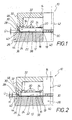
- Figur 1 zeigt abschnittweise und teilweise aufgeschnitten ein Leistungsmodul 10 mit einem Modul-Plattenelement 12 und einem becherförmigen Gehäuse 14. Das Modul-Plattenelement 12 weist ein plattenförmiges Substrat 16, beispielsweise aus einer Sinterkeramik, wie Aluminiumoxid, auf.
- An der Innenseite 18 des Substrats 16 sind Leiterbahnstrukturen 20 vorgesehen, an welchen nicht dargestellte Leistungshalbleiter-Bauelemente sowie elektrische und/oder elektronische Bauelemente kontaktiert sind. An der der Innenseite 18 gegenüberliegenden Aussenseite 22 des plattenförmigen Substrats 16 ist eine Metallisierung 24 vorgesehen, die eine Wärmeableitung vom plattenförmigen Substrat 16 zu einem abschnittweise gezeichneten Kühlkörper 26 bildet.
- Das becherförmige Gehäuse 14 weist - wie auch aus Figur 3 ersichtlich ist-einen umlaufenden Becherrand 28 auf. Der Becherrand 28 ist abgestuft mit einem umlaufenden erhöhten Aussenrand 30 und einem gegen den Aussenrand 30 zurück versetzten vertieften Innenrand 32 ausgebildet. Der Innenrand 32 ist mit voneinander und vom Aussenrand 30 beabstandeten Erhebungen 34 ausgebildet. Das Modul-Plattenelement 12, d.h. sein plattenförmiges Substrat 16, liegt im zusammengebauten Zustand des Leistungsmoduls 10 mit seinem innenseitigen Rand 36 an den Erhebungen 34 an.
- Das Modul-Plattenelement 12 steht mit seiner durch die Metallisierung 24 bestimmten Aussenfläche 38 über den Aussenrand 30 des Gehäuses 14 um ein bestimmtes Überstandsmass U über.
- Um ein unerwünschtes Verdrehen des Modul-Plattenelements 12 in Bezug zum becherförmigen Gehäuse 14 bei der Montage des Leistungsmoduls 10, d.h. bei seiner Befestigung am Kühlkörper 26, zu vermeiden, sind am Aussenrand 30 des Becherrandes 28 des Gehäuses 14 voneinander beabstandet Verdrehsicherungsnoppen 40 ausgebildet (sh. auch Figur 3). Die Verdrehsicherungsnoppen 40 stehen vom Aussenrand 30 in die gleiche Richtung weg wie die am Innenrand 32 ausgebildeten Erhebungen 34.
- Eine Verdrehung des Modul-Plattenelements 12 in Bezug zum becherförmigen Gehäuse 14, wie sie oben erwähnt worden ist, könnte sich - ohne die Ausbildung des becherförmigen Gehäuses 14 mit den Verdrehsicherungsnoppen 40 - bei der Verschraubung des Leistungsmoduls 10 mit dem Kühlkörper 26 ergeben. Eine solche an sich übliche Verschraubung ist in Figur 1 durch die strichpunktierte Linie 42 schematisch angedeutet.
- Bei dem in Figur 1 schematisch verdeutlichten Ausführungsbeispiel besitzen die Verdrehsicherungsnoppen 40 eine Höhenabmessung, die gleich gross oder geringfügig grösser ist als das Überstandsmass U des Modul-Plattenelements 12 in Bezug zum Aussenrand 30 des Becherrandes 28 des Gehäuses 14.
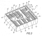
- Dem gegenüber verdeutlicht die Figur 2 eine Ausführungsform, bei der die Verdrehsicherungsnoppen 40 eine Höhenabmessung H besitzen, die geringfügig kleiner ist als das Überstandsmass U des Modul-Plattenelements 12 in Bezug zum Aussenrand 30 des Becherrandes 28 des Gehäuses 14.
- Gleiche Einzelheiten sind in Figur 2 mit denselben Bezugsziffern wie in Figur 1 bezeichnet, so dass es sich erübrigt, in Verbindung mit Figur 2 alle Einzelheiten noch einmal detailliert zu beschreiben.
- Die Verdrehsicherungsnoppen 40 können beispielsweise pyramidenstumpfförmig oder kegelstumpfförmig ausgebildet sein. Die Verdrehsicherungsnoppen 40 können auch als kleine Quader gestaltet sein. Unabhängig von der jeweiligen Ausbildung der Verdrehsicherungsnoppen 40 sind diese innenseitig mit einer Innenfläche 44 ausgebildet, die mit der Abstufungsfläche 46 zwischen dem Aussenrand 30 und dem Innenrand 32 des Becherrandes 28 des Gehäuses 14 ebenflächig fluchtet.
-
- 10
- Leistungsmodul
- 12
- Modul-Plattenelement (von 10)
- 14
- becherförmiges Gehäuse (von 10 für 12)
- 16
- plattenförmiges Substrat (von 12)
- 18
- Innenseite (von 16)
- 20
- Leiterbahnstrukturen (an 18)
- 22
- Aussenseite (von 16)
- 24
- Metallisierung (an 22 für 26)
- 26
- Kühlkörper
- 28
- Becherrand (von 14)
- 30
- Aussenrand (von 28)
- 32
- Innenrand (von 28)
- 34
- Erhebungen (an 32)
- 36
- innenseitiger Rand (von 12 bzw. 16)
- 38
- Aussenfläche (von 12 bzw. 24)
- 40
- Verdrehsicherungsnoppen (an 30)
- 42
- strichpunktierte Linie /Verschraubung (von 10 mit 26)
- 44
- Innenfläche (von 40)
- 38
- Abstufungsfläche (zwischen 30 uns 32)
Claims (8)
- Leistungsmodul (10) mit einem Modul-Plattenelement (12) und einem becherförmigen Gehäuse (14), wobei der Becherrand (28) des Gehäuses (14) abgestuft mit einem umlaufenden erhöhten Aussenrand (30) und einem gegen den Aussenrand (30) zurück versetzten, vertieften Innenrand (32) ausgebildet ist, wobei das Modul-Plattenelement (12) mit seinem innenseitigen Rand (36) an Erhebungen (34) anliegt und mit seiner Aussenfläche (38) über den Aussenrand (30) des Gehäuses (14) um ein bestimmtes Überstandsmass (U) übersteht,
dadurch gekennzeichnet,
dass am Aussenrand (30) des Becherrandes (28) des Gehäuses (14) voneinander beabstandet Verdrehsicherungsnoppen (40) ausgebildet sind. - Leistungsmodul nach Anspruch 1,
dadurch gekennzeichnet ,
dass die Verdrehsicherungsnoppen (40) eine Höhenabmessung (H) besitzen, die an das Überstandsmass (U) des Modul-Plattenelements (12) in Bezug zum Aussenrand (30) des Becherrands (28) des Gehäuses (14) angepasst ist. - Leistungsmodul nach Anspruch 1 oder 2,
dadurch gekennzeichnet ,
dass die Verdrehsicherungsnoppen (40) eine Höhenabmessung (H) besitzen, die geringfügig kleiner ist als das Überstandsmass (U) des Modul-Plattenelements (12) in Bezug zum Aussenrand (30) des Becherrands (28) des Gehäuses (14). - Leistungsmodul nach Anspruch 1 oder 2,
dadurch gekennzeichnet ,
dass die Verdrehsicherungsnoppen (40) eine Höhenabmessung (H) besitzen, die gleich gross oder geringfügig grösser ist als das Überstandsmass (U) des Modul-Plattenelements (12) in Bezug zum Aussenrand (30) des Becherrands (30) des Gehäuses (14). - Leistungsmodul nach Anspruch 4,
dadurch gekennzeichnet ,
dass die Verdrehsicherungsnoppen (40) eine bestimmte Nachgiebigkeit besitzen. - Leistungsmodul nach einem der Ansprüche 1 bis 5,
dadurch gekennzeichnet ,
dass die Verdrehsicherungsnoppen (40) pyramidenstumpfförmig ausgebildet sind. - Leistungsmodul nach einem der Ansprüche 1 bis 5,
dadurch gekennzeichnet
dass die Verdrehsicherungsnoppen (40) kegelstumpfförmig ausgebildet sind. - Leistungsmodul nach einem der Ansprüche 1 bis 7,
dadurch gekennzeichnet ,
dass die Verdrehsicherungsnoppen (40) innenseitig mit einer Innenfläche (44) ausgebildet sind, die mit der Abstufungsfläche (46) zwischen dem Aussenrand (30) und dem Innenrand (32) des Becherrandes (28) des Gehäuses (14) ebenflächig fluchtet.
Applications Claiming Priority (1)
| Application Number | Priority Date | Filing Date | Title |
|---|---|---|---|
| DE200610052607 DE102006052607A1 (de) | 2006-11-08 | 2006-11-08 | Leistungsmodul |
Publications (3)
| Publication Number | Publication Date |
|---|---|
| EP1921909A2 true EP1921909A2 (de) | 2008-05-14 |
| EP1921909A3 EP1921909A3 (de) | 2009-12-02 |
| EP1921909B1 EP1921909B1 (de) | 2012-08-22 |
Family
ID=39050688
Family Applications (1)
| Application Number | Title | Priority Date | Filing Date |
|---|---|---|---|
| EP20070021364 Active EP1921909B1 (de) | 2006-11-08 | 2007-11-02 | Leistungsmodul |
Country Status (4)
| Country | Link |
|---|---|
| EP (1) | EP1921909B1 (de) |
| JP (1) | JP5235068B2 (de) |
| DE (1) | DE102006052607A1 (de) |
| DK (1) | DK1921909T3 (de) |
Cited By (1)
| Publication number | Priority date | Publication date | Assignee | Title |
|---|---|---|---|---|
| EP1995779A3 (de) * | 2007-05-24 | 2011-01-05 | SEMIKRON Elektronik GmbH & Co. KG | Leistungshalbleitermodul |
Citations (2)
| Publication number | Priority date | Publication date | Assignee | Title |
|---|---|---|---|---|
| JPH08145019A (ja) | 1994-11-17 | 1996-06-04 | Sumitomo Wiring Syst Ltd | 板状物品のケース内固定構造 |
| EP1037351A1 (de) | 1999-03-11 | 2000-09-20 | Robert Bosch Gmbh | Halterahmen zur Festlegung eines Bauteils an einer Wand |
Family Cites Families (4)
| Publication number | Priority date | Publication date | Assignee | Title |
|---|---|---|---|---|
| JPH07272154A (ja) * | 1994-03-30 | 1995-10-20 | Nohmi Bosai Ltd | 火災報知設備用機器 |
| DE19630173C2 (de) * | 1996-07-26 | 2001-02-08 | Semikron Elektronik Gmbh | Leistungsmodul mit Halbleiterbauelementen |
| JP4095307B2 (ja) * | 2002-02-06 | 2008-06-04 | 株式会社ケーヒン | 電子回路ユニットおよびその製造方法 |
| DE102005022402A1 (de) * | 2005-05-13 | 2006-11-23 | Robert Bosch Gmbh | Befestigungsvorrichtung |
-
2006
- 2006-11-08 DE DE200610052607 patent/DE102006052607A1/de not_active Withdrawn
-
2007
- 2007-10-25 JP JP2007277605A patent/JP5235068B2/ja active Active
- 2007-11-02 DK DK07021364T patent/DK1921909T3/da active
- 2007-11-02 EP EP20070021364 patent/EP1921909B1/de active Active
Patent Citations (2)
| Publication number | Priority date | Publication date | Assignee | Title |
|---|---|---|---|---|
| JPH08145019A (ja) | 1994-11-17 | 1996-06-04 | Sumitomo Wiring Syst Ltd | 板状物品のケース内固定構造 |
| EP1037351A1 (de) | 1999-03-11 | 2000-09-20 | Robert Bosch Gmbh | Halterahmen zur Festlegung eines Bauteils an einer Wand |
Cited By (1)
| Publication number | Priority date | Publication date | Assignee | Title |
|---|---|---|---|---|
| EP1995779A3 (de) * | 2007-05-24 | 2011-01-05 | SEMIKRON Elektronik GmbH & Co. KG | Leistungshalbleitermodul |
Also Published As
| Publication number | Publication date |
|---|---|
| DK1921909T3 (da) | 2012-11-19 |
| JP5235068B2 (ja) | 2013-07-10 |
| DE102006052607A1 (de) | 2008-05-15 |
| EP1921909A3 (de) | 2009-12-02 |
| JP2008124454A (ja) | 2008-05-29 |
| EP1921909B1 (de) | 2012-08-22 |
Similar Documents
| Publication | Publication Date | Title |
|---|---|---|
| DE10162749B4 (de) | Schaltungsanordnung | |
| DE202010014106U1 (de) | Wärmeverteiler mit flexibel gelagertem Wärmerohr | |
| DE102005050327A1 (de) | Auf einem Fahrzeug befestigte Antenne | |
| DE102011002535A1 (de) | Halbleitervorrichtung | |
| EP2227929B1 (de) | Elektronikeinheit mit einem gehäuse | |
| DE20115922U1 (de) | Kunststoff-Schaltplatte eines hydraulischen Kraftfahrzeug-Getriebesteuergerätes | |
| DE112016000817T5 (de) | Substrateinheit | |
| EP1791177A1 (de) | Halbleitereinheit mit verbesserter Wärmekopplungsanordnung | |
| EP1921909A2 (de) | Leistungsmodul | |
| EP2893785B1 (de) | Anordnung eines elektrischen steuergeräts an eine schaltplatte | |
| DE102019134161A1 (de) | Elektronikmodul für ein Elektrowerkzeug | |
| EP2827464B1 (de) | Elektrisches/elektronisches Installationsgerät | |
| DE102016221728A1 (de) | Leistungselektronikeinheit mit einem eine Hochvoltseite von einer Niedervoltseite entkoppelnden Trennelement | |
| DE102016107898A1 (de) | Laterale Leiterplattenverbindung | |
| DE19734128C5 (de) | Kunststoffgehäuse mit einem Metalleinlegeteil in einem Montageflansch | |
| DE102013207552A1 (de) | Halbleitermodul | |
| DE2855265A1 (de) | Thyristor | |
| DE102016205966A1 (de) | Elektronische Einheit mit ESD-Schutzanordnung | |
| DE10228633B4 (de) | Vorrichtung zum Schutz vor elektrostatischer Entladung und elektromagnetischer Einflüsse | |
| DE102015207327A1 (de) | Schaltungsanordnung für eine elektronische Schaltung | |
| DE102014208594A1 (de) | Leistungselektronikanordnung | |
| DE102008021606B4 (de) | Tastaturmatte | |
| DE102016205151B4 (de) | Träger mit einer auf dem Träger befestigten Leiterplatte | |
| DE102019219560A1 (de) | Gehäuse für zumindest ein elektronisches Bauteil | |
| DE4009289A1 (de) | Elektronisches einschubteil zum einschieben in den rahmen eines schaltschrankes |
Legal Events
| Date | Code | Title | Description |
|---|---|---|---|
| PUAI | Public reference made under article 153(3) epc to a published international application that has entered the european phase |
Free format text: ORIGINAL CODE: 0009012 |
|
| AK | Designated contracting states |
Kind code of ref document: A2 Designated state(s): AT BE BG CH CY CZ DE DK EE ES FI FR GB GR HU IE IS IT LI LT LU LV MC MT NL PL PT RO SE SI SK TR |
|
| AX | Request for extension of the european patent |
Extension state: AL BA HR MK RS |
|
| PUAL | Search report despatched |
Free format text: ORIGINAL CODE: 0009013 |
|
| AK | Designated contracting states |
Kind code of ref document: A3 Designated state(s): AT BE BG CH CY CZ DE DK EE ES FI FR GB GR HU IE IS IT LI LT LU LV MC MT NL PL PT RO SE SI SK TR |
|
| AX | Request for extension of the european patent |
Extension state: AL BA HR MK RS |
|
| 17P | Request for examination filed |
Effective date: 20091105 |
|
| 17Q | First examination report despatched |
Effective date: 20091211 |
|
| AKX | Designation fees paid |
Designated state(s): AT BE BG CH CY CZ DE DK EE ES FI FR GB GR HU IE IS IT LI LT LU LV MC MT NL PL PT RO SE SI SK TR |
|
| GRAP | Despatch of communication of intention to grant a patent |
Free format text: ORIGINAL CODE: EPIDOSNIGR1 |
|
| GRAS | Grant fee paid |
Free format text: ORIGINAL CODE: EPIDOSNIGR3 |
|
| GRAA | (expected) grant |
Free format text: ORIGINAL CODE: 0009210 |
|
| AK | Designated contracting states |
Kind code of ref document: B1 Designated state(s): AT BE BG CH CY CZ DE DK EE ES FI FR GB GR HU IE IS IT LI LT LU LV MC MT NL PL PT RO SE SI SK TR |
|
| REG | Reference to a national code |
Ref country code: GB Ref legal event code: FG4D Free format text: NOT ENGLISH |
|
| REG | Reference to a national code |
Ref country code: CH Ref legal event code: EP |
|
| REG | Reference to a national code |
Ref country code: IE Ref legal event code: FG4D Free format text: LANGUAGE OF EP DOCUMENT: GERMAN |
|
| REG | Reference to a national code |
Ref country code: CH Ref legal event code: NV Representative=s name: BRAUNPAT BRAUN EDER AG |
|
| REG | Reference to a national code |
Ref country code: AT Ref legal event code: REF Ref document number: 572522 Country of ref document: AT Kind code of ref document: T Effective date: 20120915 |
|
| REG | Reference to a national code |
Ref country code: DE Ref legal event code: R096 Ref document number: 502007010415 Country of ref document: DE Effective date: 20121018 |
|
| REG | Reference to a national code |
Ref country code: DK Ref legal event code: T3 |
|
| REG | Reference to a national code |
Ref country code: NL Ref legal event code: T3 |
|
| REG | Reference to a national code |
Ref country code: SK Ref legal event code: T3 Ref document number: E 12800 Country of ref document: SK |
|
| REG | Reference to a national code |
Ref country code: LT Ref legal event code: MG4D Effective date: 20120801 |
|
| PG25 | Lapsed in a contracting state [announced via postgrant information from national office to epo] |
Ref country code: IS Free format text: LAPSE BECAUSE OF FAILURE TO SUBMIT A TRANSLATION OF THE DESCRIPTION OR TO PAY THE FEE WITHIN THE PRESCRIBED TIME-LIMIT Effective date: 20121222 Ref country code: CY Free format text: LAPSE BECAUSE OF FAILURE TO SUBMIT A TRANSLATION OF THE DESCRIPTION OR TO PAY THE FEE WITHIN THE PRESCRIBED TIME-LIMIT Effective date: 20120822 Ref country code: LT Free format text: LAPSE BECAUSE OF FAILURE TO SUBMIT A TRANSLATION OF THE DESCRIPTION OR TO PAY THE FEE WITHIN THE PRESCRIBED TIME-LIMIT Effective date: 20120822 Ref country code: FI Free format text: LAPSE BECAUSE OF FAILURE TO SUBMIT A TRANSLATION OF THE DESCRIPTION OR TO PAY THE FEE WITHIN THE PRESCRIBED TIME-LIMIT Effective date: 20120822 |
|
| PG25 | Lapsed in a contracting state [announced via postgrant information from national office to epo] |
Ref country code: GR Free format text: LAPSE BECAUSE OF FAILURE TO SUBMIT A TRANSLATION OF THE DESCRIPTION OR TO PAY THE FEE WITHIN THE PRESCRIBED TIME-LIMIT Effective date: 20121123 Ref country code: PT Free format text: LAPSE BECAUSE OF FAILURE TO SUBMIT A TRANSLATION OF THE DESCRIPTION OR TO PAY THE FEE WITHIN THE PRESCRIBED TIME-LIMIT Effective date: 20121224 Ref country code: SE Free format text: LAPSE BECAUSE OF FAILURE TO SUBMIT A TRANSLATION OF THE DESCRIPTION OR TO PAY THE FEE WITHIN THE PRESCRIBED TIME-LIMIT Effective date: 20120822 Ref country code: LV Free format text: LAPSE BECAUSE OF FAILURE TO SUBMIT A TRANSLATION OF THE DESCRIPTION OR TO PAY THE FEE WITHIN THE PRESCRIBED TIME-LIMIT Effective date: 20120822 Ref country code: SI Free format text: LAPSE BECAUSE OF FAILURE TO SUBMIT A TRANSLATION OF THE DESCRIPTION OR TO PAY THE FEE WITHIN THE PRESCRIBED TIME-LIMIT Effective date: 20120822 |
|
| PG25 | Lapsed in a contracting state [announced via postgrant information from national office to epo] |
Ref country code: CZ Free format text: LAPSE BECAUSE OF FAILURE TO SUBMIT A TRANSLATION OF THE DESCRIPTION OR TO PAY THE FEE WITHIN THE PRESCRIBED TIME-LIMIT Effective date: 20120822 Ref country code: RO Free format text: LAPSE BECAUSE OF FAILURE TO SUBMIT A TRANSLATION OF THE DESCRIPTION OR TO PAY THE FEE WITHIN THE PRESCRIBED TIME-LIMIT Effective date: 20120822 Ref country code: EE Free format text: LAPSE BECAUSE OF FAILURE TO SUBMIT A TRANSLATION OF THE DESCRIPTION OR TO PAY THE FEE WITHIN THE PRESCRIBED TIME-LIMIT Effective date: 20120822 Ref country code: ES Free format text: LAPSE BECAUSE OF FAILURE TO SUBMIT A TRANSLATION OF THE DESCRIPTION OR TO PAY THE FEE WITHIN THE PRESCRIBED TIME-LIMIT Effective date: 20121203 |
|
| BERE | Be: lapsed |
Owner name: SEMIKRON ELEKTRONIK G.M.B.H. & CO. KG Effective date: 20121130 |
|
| PG25 | Lapsed in a contracting state [announced via postgrant information from national office to epo] |
Ref country code: PL Free format text: LAPSE BECAUSE OF FAILURE TO SUBMIT A TRANSLATION OF THE DESCRIPTION OR TO PAY THE FEE WITHIN THE PRESCRIBED TIME-LIMIT Effective date: 20120822 |
|
| PLBE | No opposition filed within time limit |
Free format text: ORIGINAL CODE: 0009261 |
|
| STAA | Information on the status of an ep patent application or granted ep patent |
Free format text: STATUS: NO OPPOSITION FILED WITHIN TIME LIMIT |
|
| REG | Reference to a national code |
Ref country code: HU Ref legal event code: AG4A Ref document number: E015715 Country of ref document: HU |
|
| 26N | No opposition filed |
Effective date: 20130523 |
|
| PG25 | Lapsed in a contracting state [announced via postgrant information from national office to epo] |
Ref country code: BG Free format text: LAPSE BECAUSE OF FAILURE TO SUBMIT A TRANSLATION OF THE DESCRIPTION OR TO PAY THE FEE WITHIN THE PRESCRIBED TIME-LIMIT Effective date: 20121122 |
|
| REG | Reference to a national code |
Ref country code: IE Ref legal event code: MM4A |
|
| PG25 | Lapsed in a contracting state [announced via postgrant information from national office to epo] |
Ref country code: BE Free format text: LAPSE BECAUSE OF NON-PAYMENT OF DUE FEES Effective date: 20121130 |
|
| REG | Reference to a national code |
Ref country code: DE Ref legal event code: R097 Ref document number: 502007010415 Country of ref document: DE Effective date: 20130523 |
|
| PG25 | Lapsed in a contracting state [announced via postgrant information from national office to epo] |
Ref country code: IE Free format text: LAPSE BECAUSE OF NON-PAYMENT OF DUE FEES Effective date: 20121102 |
|
| PG25 | Lapsed in a contracting state [announced via postgrant information from national office to epo] |
Ref country code: MT Free format text: LAPSE BECAUSE OF FAILURE TO SUBMIT A TRANSLATION OF THE DESCRIPTION OR TO PAY THE FEE WITHIN THE PRESCRIBED TIME-LIMIT Effective date: 20120822 |
|
| REG | Reference to a national code |
Ref country code: AT Ref legal event code: MM01 Ref document number: 572522 Country of ref document: AT Kind code of ref document: T Effective date: 20121130 |
|
| PG25 | Lapsed in a contracting state [announced via postgrant information from national office to epo] |
Ref country code: AT Free format text: LAPSE BECAUSE OF NON-PAYMENT OF DUE FEES Effective date: 20121130 |
|
| PG25 | Lapsed in a contracting state [announced via postgrant information from national office to epo] |
Ref country code: MC Free format text: LAPSE BECAUSE OF NON-PAYMENT OF DUE FEES Effective date: 20121130 Ref country code: TR Free format text: LAPSE BECAUSE OF FAILURE TO SUBMIT A TRANSLATION OF THE DESCRIPTION OR TO PAY THE FEE WITHIN THE PRESCRIBED TIME-LIMIT Effective date: 20120822 |
|
| PG25 | Lapsed in a contracting state [announced via postgrant information from national office to epo] |
Ref country code: LU Free format text: LAPSE BECAUSE OF NON-PAYMENT OF DUE FEES Effective date: 20121102 |
|
| REG | Reference to a national code |
Ref country code: FR Ref legal event code: PLFP Year of fee payment: 9 |
|
| REG | Reference to a national code |
Ref country code: FR Ref legal event code: PLFP Year of fee payment: 10 |
|
| PGFP | Annual fee paid to national office [announced via postgrant information from national office to epo] |
Ref country code: DK Payment date: 20161124 Year of fee payment: 10 Ref country code: HU Payment date: 20161025 Year of fee payment: 10 Ref country code: SK Payment date: 20161026 Year of fee payment: 10 Ref country code: NL Payment date: 20161124 Year of fee payment: 10 |
|
| REG | Reference to a national code |
Ref country code: FR Ref legal event code: PLFP Year of fee payment: 11 |
|
| REG | Reference to a national code |
Ref country code: CH Ref legal event code: PCAR Free format text: NEW ADDRESS: HOLEESTRASSE 87, 4054 BASEL (CH) |
|
| REG | Reference to a national code |
Ref country code: DK Ref legal event code: EBP Effective date: 20171130 |
|
| REG | Reference to a national code |
Ref country code: NL Ref legal event code: MM Effective date: 20171201 |
|
| PG25 | Lapsed in a contracting state [announced via postgrant information from national office to epo] |
Ref country code: SK Free format text: LAPSE BECAUSE OF NON-PAYMENT OF DUE FEES Effective date: 20171102 |
|
| REG | Reference to a national code |
Ref country code: SK Ref legal event code: MM4A Ref document number: E 12800 Country of ref document: SK Effective date: 20171102 |
|
| PG25 | Lapsed in a contracting state [announced via postgrant information from national office to epo] |
Ref country code: HU Free format text: LAPSE BECAUSE OF NON-PAYMENT OF DUE FEES Effective date: 20171103 |
|
| PG25 | Lapsed in a contracting state [announced via postgrant information from national office to epo] |
Ref country code: NL Free format text: LAPSE BECAUSE OF NON-PAYMENT OF DUE FEES Effective date: 20171201 |
|
| PG25 | Lapsed in a contracting state [announced via postgrant information from national office to epo] |
Ref country code: DK Free format text: LAPSE BECAUSE OF NON-PAYMENT OF DUE FEES Effective date: 20171130 |
|
| REG | Reference to a national code |
Ref country code: DE Ref legal event code: R081 Ref document number: 502007010415 Country of ref document: DE Owner name: SEMIKRON DANFOSS ELEKTRONIK GMBH & CO. KG, DE Free format text: FORMER OWNER: SEMIKRON ELEKTRONIK GMBH & CO. KG, 90431 NUERNBERG, DE |
|
| REG | Reference to a national code |
Ref country code: CH Ref legal event code: U11 Free format text: ST27 STATUS EVENT CODE: U-0-0-U10-U11 (AS PROVIDED BY THE NATIONAL OFFICE) Effective date: 20251201 |
|
| PGFP | Annual fee paid to national office [announced via postgrant information from national office to epo] |
Ref country code: DE Payment date: 20251007 Year of fee payment: 19 |
|
| PGFP | Annual fee paid to national office [announced via postgrant information from national office to epo] |
Ref country code: GB Payment date: 20251016 Year of fee payment: 19 |
|
| PGFP | Annual fee paid to national office [announced via postgrant information from national office to epo] |
Ref country code: IT Payment date: 20251022 Year of fee payment: 19 |
|
| PGFP | Annual fee paid to national office [announced via postgrant information from national office to epo] |
Ref country code: FR Payment date: 20251008 Year of fee payment: 19 |
|
| PGFP | Annual fee paid to national office [announced via postgrant information from national office to epo] |
Ref country code: CH Payment date: 20251201 Year of fee payment: 19 |