EP1921640B1 - Spiralförmiger geschlossener magnetischer Kern und integrierte Microinduktanz mit einem solchen geschlossenen magnetischen Kern - Google Patents
Spiralförmiger geschlossener magnetischer Kern und integrierte Microinduktanz mit einem solchen geschlossenen magnetischen Kern Download PDFInfo
- Publication number
- EP1921640B1 EP1921640B1 EP07354060A EP07354060A EP1921640B1 EP 1921640 B1 EP1921640 B1 EP 1921640B1 EP 07354060 A EP07354060 A EP 07354060A EP 07354060 A EP07354060 A EP 07354060A EP 1921640 B1 EP1921640 B1 EP 1921640B1
- Authority
- EP
- European Patent Office
- Prior art keywords
- magnetic core
- branches
- inductance
- core
- spiral
- Prior art date
- Legal status (The legal status is an assumption and is not a legal conclusion. Google has not performed a legal analysis and makes no representation as to the accuracy of the status listed.)
- Not-in-force
Links
- 230000005291 magnetic effect Effects 0.000 title claims description 58
- 238000004804 winding Methods 0.000 description 11
- 239000000696 magnetic material Substances 0.000 description 6
- 238000004519 manufacturing process Methods 0.000 description 6
- PXHVJJICTQNCMI-UHFFFAOYSA-N Nickel Chemical compound [Ni] PXHVJJICTQNCMI-UHFFFAOYSA-N 0.000 description 5
- 238000000034 method Methods 0.000 description 4
- 230000004907 flux Effects 0.000 description 3
- 229910052782 aluminium Inorganic materials 0.000 description 2
- 230000001609 comparable effect Effects 0.000 description 2
- 239000010949 copper Substances 0.000 description 2
- 230000007423 decrease Effects 0.000 description 2
- 230000006872 improvement Effects 0.000 description 2
- 230000001965 increasing effect Effects 0.000 description 2
- 230000001939 inductive effect Effects 0.000 description 2
- 238000004377 microelectronic Methods 0.000 description 2
- 229910052759 nickel Inorganic materials 0.000 description 2
- 238000004806 packaging method and process Methods 0.000 description 2
- BASFCYQUMIYNBI-UHFFFAOYSA-N platinum Chemical compound [Pt] BASFCYQUMIYNBI-UHFFFAOYSA-N 0.000 description 2
- 230000008569 process Effects 0.000 description 2
- 229920006395 saturated elastomer Polymers 0.000 description 2
- 239000010936 titanium Substances 0.000 description 2
- 229910018072 Al 2 O 3 Inorganic materials 0.000 description 1
- RYGMFSIKBFXOCR-UHFFFAOYSA-N Copper Chemical compound [Cu] RYGMFSIKBFXOCR-UHFFFAOYSA-N 0.000 description 1
- 101100422538 Escherichia coli sat-2 gene Proteins 0.000 description 1
- XEEYBQQBJWHFJM-UHFFFAOYSA-N Iron Chemical compound [Fe] XEEYBQQBJWHFJM-UHFFFAOYSA-N 0.000 description 1
- 229910000914 Mn alloy Inorganic materials 0.000 description 1
- 229910003289 NiMn Inorganic materials 0.000 description 1
- 229910019041 PtMn Inorganic materials 0.000 description 1
- KJTLSVCANCCWHF-UHFFFAOYSA-N Ruthenium Chemical compound [Ru] KJTLSVCANCCWHF-UHFFFAOYSA-N 0.000 description 1
- 229910004298 SiO 2 Inorganic materials 0.000 description 1
- VYPSYNLAJGMNEJ-UHFFFAOYSA-N Silicium dioxide Chemical compound O=[Si]=O VYPSYNLAJGMNEJ-UHFFFAOYSA-N 0.000 description 1
- RTAQQCXQSZGOHL-UHFFFAOYSA-N Titanium Chemical compound [Ti] RTAQQCXQSZGOHL-UHFFFAOYSA-N 0.000 description 1
- 238000004026 adhesive bonding Methods 0.000 description 1
- 229910045601 alloy Inorganic materials 0.000 description 1
- 239000000956 alloy Substances 0.000 description 1
- XAGFODPZIPBFFR-UHFFFAOYSA-N aluminium Chemical compound [Al] XAGFODPZIPBFFR-UHFFFAOYSA-N 0.000 description 1
- 230000005290 antiferromagnetic effect Effects 0.000 description 1
- 239000002885 antiferromagnetic material Substances 0.000 description 1
- 229910052796 boron Inorganic materials 0.000 description 1
- 238000006243 chemical reaction Methods 0.000 description 1
- 229910017052 cobalt Inorganic materials 0.000 description 1
- 239000010941 cobalt Substances 0.000 description 1
- GUTLYIVDDKVIGB-UHFFFAOYSA-N cobalt atom Chemical compound [Co] GUTLYIVDDKVIGB-UHFFFAOYSA-N 0.000 description 1
- 239000004020 conductor Substances 0.000 description 1
- 229910052802 copper Inorganic materials 0.000 description 1
- 238000000151 deposition Methods 0.000 description 1
- 230000008021 deposition Effects 0.000 description 1
- 239000003989 dielectric material Substances 0.000 description 1
- 230000000694 effects Effects 0.000 description 1
- 238000004870 electrical engineering Methods 0.000 description 1
- 238000005530 etching Methods 0.000 description 1
- 230000005294 ferromagnetic effect Effects 0.000 description 1
- 238000001914 filtration Methods 0.000 description 1
- 230000014509 gene expression Effects 0.000 description 1
- 229910052735 hafnium Inorganic materials 0.000 description 1
- 238000003780 insertion Methods 0.000 description 1
- 230000037431 insertion Effects 0.000 description 1
- 239000011810 insulating material Substances 0.000 description 1
- 230000010354 integration Effects 0.000 description 1
- 229910052741 iridium Inorganic materials 0.000 description 1
- GKOZUEZYRPOHIO-UHFFFAOYSA-N iridium atom Chemical compound [Ir] GKOZUEZYRPOHIO-UHFFFAOYSA-N 0.000 description 1
- 238000002955 isolation Methods 0.000 description 1
- 239000011572 manganese Substances 0.000 description 1
- 229910052751 metal Inorganic materials 0.000 description 1
- 239000002184 metal Substances 0.000 description 1
- 238000005459 micromachining Methods 0.000 description 1
- 229910000480 nickel oxide Inorganic materials 0.000 description 1
- 229910052757 nitrogen Inorganic materials 0.000 description 1
- 238000005457 optimization Methods 0.000 description 1
- TWNQGVIAIRXVLR-UHFFFAOYSA-N oxo(oxoalumanyloxy)alumane Chemical compound O=[Al]O[Al]=O TWNQGVIAIRXVLR-UHFFFAOYSA-N 0.000 description 1
- GNRSAWUEBMWBQH-UHFFFAOYSA-N oxonickel Chemical compound [Ni]=O GNRSAWUEBMWBQH-UHFFFAOYSA-N 0.000 description 1
- 229910052760 oxygen Inorganic materials 0.000 description 1
- 230000035699 permeability Effects 0.000 description 1
- 238000000206 photolithography Methods 0.000 description 1
- 229910052697 platinum Inorganic materials 0.000 description 1
- 230000000630 rising effect Effects 0.000 description 1
- 229910052707 ruthenium Inorganic materials 0.000 description 1
- 229910052710 silicon Inorganic materials 0.000 description 1
- 229910052814 silicon oxide Inorganic materials 0.000 description 1
- 238000004088 simulation Methods 0.000 description 1
- 239000000758 substrate Substances 0.000 description 1
- 229910052715 tantalum Inorganic materials 0.000 description 1
- GUVRBAGPIYLISA-UHFFFAOYSA-N tantalum atom Chemical compound [Ta] GUVRBAGPIYLISA-UHFFFAOYSA-N 0.000 description 1
- 238000007736 thin film deposition technique Methods 0.000 description 1
- 229910052719 titanium Inorganic materials 0.000 description 1
Images

Classifications
-
- H—ELECTRICITY
- H01—ELECTRIC ELEMENTS
- H01F—MAGNETS; INDUCTANCES; TRANSFORMERS; SELECTION OF MATERIALS FOR THEIR MAGNETIC PROPERTIES
- H01F17/00—Fixed inductances of the signal type
- H01F17/0006—Printed inductances
- H01F17/0033—Printed inductances with the coil helically wound around a magnetic core
-
- H—ELECTRICITY
- H01—ELECTRIC ELEMENTS
- H01F—MAGNETS; INDUCTANCES; TRANSFORMERS; SELECTION OF MATERIALS FOR THEIR MAGNETIC PROPERTIES
- H01F17/00—Fixed inductances of the signal type
- H01F17/04—Fixed inductances of the signal type with magnetic core
-
- H—ELECTRICITY
- H01—ELECTRIC ELEMENTS
- H01F—MAGNETS; INDUCTANCES; TRANSFORMERS; SELECTION OF MATERIALS FOR THEIR MAGNETIC PROPERTIES
- H01F17/00—Fixed inductances of the signal type
- H01F17/04—Fixed inductances of the signal type with magnetic core
- H01F17/045—Fixed inductances of the signal type with magnetic core with core of cylindric geometry and coil wound along its longitudinal axis, i.e. rod or drum core
-
- H—ELECTRICITY
- H01—ELECTRIC ELEMENTS
- H01F—MAGNETS; INDUCTANCES; TRANSFORMERS; SELECTION OF MATERIALS FOR THEIR MAGNETIC PROPERTIES
- H01F27/00—Details of transformers or inductances, in general
- H01F27/24—Magnetic cores
- H01F27/25—Magnetic cores made from strips or ribbons
-
- H—ELECTRICITY
- H01—ELECTRIC ELEMENTS
- H01F—MAGNETS; INDUCTANCES; TRANSFORMERS; SELECTION OF MATERIALS FOR THEIR MAGNETIC PROPERTIES
- H01F41/00—Apparatus or processes specially adapted for manufacturing or assembling magnets, inductances or transformers; Apparatus or processes specially adapted for manufacturing materials characterised by their magnetic properties
- H01F41/02—Apparatus or processes specially adapted for manufacturing or assembling magnets, inductances or transformers; Apparatus or processes specially adapted for manufacturing materials characterised by their magnetic properties for manufacturing cores, coils, or magnets
- H01F41/04—Apparatus or processes specially adapted for manufacturing or assembling magnets, inductances or transformers; Apparatus or processes specially adapted for manufacturing materials characterised by their magnetic properties for manufacturing cores, coils, or magnets for manufacturing coils
- H01F41/041—Printed circuit coils
- H01F41/046—Printed circuit coils structurally combined with ferromagnetic material
Definitions
- the invention relates to a closed magnetic core for integrated micro-inductance.
- the invention is part of the theme of integrated micro-inductors for applications in power electronics. It can, more generally, apply to all inductive systems (inductors, transformers, magnetic recording heads, actuators, sensors, etc ...) requiring a high density of electrical power.
- Micro-inductances of various types have existed for many years, using coils of the spiral or solenoid type.
- the discrete components remain very predominantly used in applications using high power densities because they offer a better compromise between inductance and saturation current.
- a spiral winding with magnetic plane is easy to integrate and allows to work with strong currents.
- this type of device becomes very cumbersome when one targets high values of inductance (L of the order of ⁇ H), because it takes a number of high spiral turns.
- the resistance of such devices is important.
- Toroidal integrated micro-inductors with solenoid windings as well as their meander improvements (see the article “Integrated Electroplated Micromachined Magnetic Devices Using Low Temperature Manufacturing Processes” by JYPark et. al., IEEE Transactions on Electronics Packaging Manufacturing, Vol. 23, No. 1, 2000 ), are directly inspired by discrete components and offer the best possible compromise between resistance and inductance level, because we approach the ideal case of the infinite solenoid.
- simulations show that the magnetic flux inside the nucleus is distributed very inhomogeneously. The magnetic field is more intense along the shorter field lines.
- the zones of the magnetic core subjected to the most intense fields are very quickly saturated, causing a decrease of the inductance from weak currents, whereas other zones are subjected to much weaker fields and participate little or not in inductive phenomenon, that is to say they have no contribution to the value of the inductance.
- the useful areas of the magnetic core are therefore very quickly saturated while other areas remain unsolicited.
- the maximum power passing through an inductor is determined by the volume of magnetic material used in the case of an integrated component. This volume is determined by the thickness of magnetic material (thicknesses less than 100 microns for integrated components) and the area occupied by this magnetic core.
- Transformers and inductors with E-shaped or E-1 magnetic core are widely used in electrical engineering, mainly in discrete transformers (and in discrete DC / DC type devices) to facilitate assembly and winding of inductors , or to be able to play on the conversion factors between the three windings of each branch, or on the effects of mutual inductances between the separate windings of each branch (see the article «New Magnetic Structures for Switching Converters by S.Cuk, IEEE Transactions on Magnetics, Vol. MAG-19, No. 2, 1983 ). In these devices, the winding is not continuous from one branch to the other, but made by separate wires.
- micro-inductors used on the market are discrete components manufactured by micromechanical processes of micro-machining, gluing, micro-winding, etc. These processes are heavy to implement, individual treatment, not very flexible in terms of design and greatly limit the miniaturization of power circuits.
- the thickness of the discrete micro-inductors typically greater than 0.5 mm does not allow appropriate packaging in the power supply circuits currently used for mobile telephony, for example.
- the manufacturing techniques used in microelectronics allow a much greater flexibility in the implementation of different designs, provide a collective treatment and are compatible with the idea of miniaturization because the thickness (including substrate) can easily be less than 300 ⁇ m). However, they are poorly suited to deposition of high thicknesses (greater than 10 ⁇ m ) of conductive, magnetic or dielectric materials and to their etching after photolithography.
- the integrated micro-inductors generally have an inductance which decreases greatly when the current applied to the turns of the micro-inductor is increased, even for weak currents, which makes it necessary to use unintegrated discrete inductors in certain cases.
- the object of the invention is to increase the compactness of a core of an integrated micro-inductance and, for a given size, to increase the value of the inductance.
- this object is achieved by a magnetic core according to the appended claims and more particularly by the fact that the magnetic core has a spiral shape having two ends connected to one another by a closing segment.
- the invention also aims an integrated micro-inductance comprising a magnetic core according to the invention.
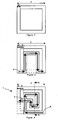
- the magnetic core 1, represented on the figure 1 has a spiral shape.
- the spiral has two ends 2 connected to each other by a closing segment 3. Thus, the magnetic core 1 is closed.
- the magnetic core 1 is constituted by a first set 4 of five parallel branches and a second set of four parallel branches, substantially perpendicular to the branches of the first set 4.
- the spiral constituted by all the branches of the two sets 4 and 5 is thus rectangular.
- the connection constituted by the closing segment 3 is added to the spiral to form the magnetic core 1.
- the magnetic core 1 makes it possible to maximize the occupation of the space in the center of the core 1 and the corresponding micro-inductance.
- FIG. figure 2 An annular inductor according to the prior art, represented in FIG. figure 2 , fits particularly well to a square-shaped chip.
- the length of the developed ring depends on the outer perimeter of the chip. This geometry does not exploit the central part of the chip.
- the figure 3 represents an improvement in the annular inductance, the meandering inductance described in the aforementioned Park article.
- the meandering inductance makes it possible to use the central zone by stretching one of the four branches of the ring so as to constitute one or more meanders covering the central part.
- This solution makes it possible to increase the length I of the constant surface core.
- the core zone occupies the meandering core ( figure 3 ) makes it possible to obtain a gain on the length I of the core of the order of 33%, with respect to the annular core ( figure 2 ).
- N of turns according to the length I of the core a compromise is obtained with a gain on the inductance L of about 20% and a gain on the saturation current I sat of about 10%.
- the meandering inductance is optimal only in special cases where the width of the ring and the width of the branches satisfy certain geometry conditions. Indeed, the central zone must be large enough to allow the insertion of an integer number of meanders.
- the core has an overall width T
- the branches have a width W
- the spacing between two adjacent branches must be greater than a minimum spacing S.
- the overall width T of the core must fill the condition : T ⁇ 2 ⁇ W + nm * 2 ⁇ W + 2 ⁇ nm + 1 * S .
- T 2 ⁇ W + nm * 2 ⁇ W + 2 ⁇ nm + 1 * S .
- the branches and the closure segment 3 have a preferential direction of propagation of the magnetic flux in dynamics.
- the magnetic axes of the branches and the closing segment 3 are oriented relative to the other, so as to obtain a flow in the form of a closed loop as shown in FIG. figure 4 by the arrows 6.
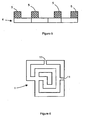
- the branches can be arranged in different parallel planes.
- the first set 4 of parallel branches is arranged in a first plane and the second set of parallel branches is arranged in a second plane parallel to the first plane and greater than the first plane on the first plane.
- the branches can have different thicknesses. So, on the figure 5 the branches of the first set 4 are less thick than the branches of the second set 5. This makes it possible in particular to adapt the core to the local constraints of the chip used and the adjacent electronic components.
- One or more air gaps may optionally cut the magnetic core 1 to increase the reluctance of the magnetic circuit.
- the magnetic core 1 shown in figure 6 has a number of gaps 11 of low dimension (at least a factor 1/10 between the dimension of the gap and the total length of the magnetic circuit).
- the gaps can be arranged in one or more branches.
- the branches form a spiral of rectangular type, or at least substantially rectangular, having two turns in two concentric rectangles. However, as needed, more complex spirals may be considered.
- the forms involved may be arbitrary, for example the geometry of the spiral is rectangular, round, square or octagonal. The person skilled in the art determines the particular form by using simulation software such as the Flux software from Cedrat or the Maxwell software from Ansoft.
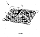
- the figure 7 illustrates a micro-inductance comprising the magnetic core 1 according to the invention.
- a plurality of disjointed turns 9 constitute a winding around the magnetic core 1.
- All the branches of the core may comprise winding turns.
- the turns envelop substantially all of the surface of the magnetic core 1, a minimum isolation gap separating the adjacent turns.
- Each turn may comprise a lower plane section in a lower plane, an upper plane section in an upper plane and two rising sections.
- the winding preferably comprises a single electrical input and a single electrical output.
- the closing segment 3 preferably has no turns 9.
- micro-inductance presents no additional manufacturing difficulties compared to conventional pre-existing systems.
- high permeability magnetic materials typically iron (Fe) and / or nickel (Ni) and / or cobalt (Co) alloys, which can contain one or more of aluminum, Al, Si, Tantalum, Hf, N, O, and B
- the core may be heterogeneous and consist of several ferromagnetic and conductive or dielectric (non-magnetic) or antiferromagnetic layers.
- the core may consist of an alternation of magnetic layers and intermediate layers, for example a stack comprising two magnetic layers separated by an intermediate layer.
- the intermediate layers may, for example, be metal (Cu copper, titanium Ti or ruthenium Ru, for example) or an insulating material such as silicon oxide SiO 2 or aluminum oxide Al 2 O 3 , for example.
- the intermediate layers may also consist of antiferromagnetic materials such as nickel oxide NiO or alloys of manganese (Mn) comprising nickel (NiMn), iridium (IrMn) or platinum (PtMn).
- the micro-inductance is not limited in its frequency of use, and may be suitable for high frequency uses, which always demand more power.
Landscapes
- Engineering & Computer Science (AREA)
- Power Engineering (AREA)
- Microelectronics & Electronic Packaging (AREA)
- Coils Or Transformers For Communication (AREA)
- Switches That Are Operated By Magnetic Or Electric Fields (AREA)
Claims (9)
- Geschlossener Magnetkern (1) für eine integrierte Mikro-Induktivität, dadurch gekennzeichnet, dass er die Form einer Spirale mit zwei Enden (2) hat, die miteinander über ein Verschlusssegment (3) verbunden sind.
- Magnetkern (1) nach Anspruch 1, dadurch gekennzeichnet, dass er die Form einer Spirale der rechteckigen Art hat.
- Magnetkern (1) nach einem der Ansprüche 1 und 2, dadurch gekennzeichnet, dass der Magnetkern (1) von einer Mehrzahl von Zweigen gebildet wird.
- Magnetkern (1) nach Anspruch 3, dadurch gekennzeichnet, dass mindestens zwei Zweige auf unterschiedlichen parallelen Ebenen angeordnet sind.
- Magnetkern (1) nach Anspruch 4, dadurch gekennzeichnet, dass ein erster Satz (4) paralleler Zweige auf einer ersten Ebene angeordnet ist und ein zweiter Satz (5) paralleler Zweige auf einer zweiten Ebene angeordnet ist.
- Magnetkern (1) nach Anspruch 5, dadurch gekennzeichnet, dass die Zweige des ersten Satzes (4) paralleler Zweige im Wesentlichen lotrecht zu den Zweigen des zweiten Satzes (5) paralleler Zweige angeordnet sind.
- Magnetkern (1) nach einem der Ansprüche 3 bis 6, dadurch gekennzeichnet, dass mindestens zwei Zweige unterschiedliche Dicken haben.
- Magnetkern (1) nach einem der Ansprüche 1 bis 7, dadurch gekennzeichnet, dass er mindestens einen Luftspalt (11) umfasst.
- Integrierte Mikro-Induktivität, dadurch gekennzeichnet, dass sie einen Magnetkern (1) nach einem der Ansprüche 1 bis 8 umfasst.
Applications Claiming Priority (1)
| Application Number | Priority Date | Filing Date | Title |
|---|---|---|---|
| FR0609714A FR2908231B1 (fr) | 2006-11-07 | 2006-11-07 | Noyau magnetique ferme en forme de spirale et micro-inductance integree comportant un tel noyau magnetique ferme |
Publications (2)
| Publication Number | Publication Date |
|---|---|
| EP1921640A1 EP1921640A1 (de) | 2008-05-14 |
| EP1921640B1 true EP1921640B1 (de) | 2009-08-26 |
Family
ID=38004847
Family Applications (1)
| Application Number | Title | Priority Date | Filing Date |
|---|---|---|---|
| EP07354060A Not-in-force EP1921640B1 (de) | 2006-11-07 | 2007-11-06 | Spiralförmiger geschlossener magnetischer Kern und integrierte Microinduktanz mit einem solchen geschlossenen magnetischen Kern |
Country Status (6)
| Country | Link |
|---|---|
| US (1) | US20080106364A1 (de) |
| EP (1) | EP1921640B1 (de) |
| JP (1) | JP2008187166A (de) |
| AT (1) | ATE441193T1 (de) |
| DE (1) | DE602007002139D1 (de) |
| FR (1) | FR2908231B1 (de) |
Families Citing this family (3)
| Publication number | Priority date | Publication date | Assignee | Title |
|---|---|---|---|---|
| US20150061815A1 (en) | 2013-09-04 | 2015-03-05 | International Business Machines Corporation | Planar inductors with closed magnetic loops |
| US10290414B2 (en) * | 2015-08-31 | 2019-05-14 | Qualcomm Incorporated | Substrate comprising an embedded inductor and a thin film magnetic core |
| US10600566B2 (en) | 2016-10-13 | 2020-03-24 | International Business Machines Corporation | Method for forming a planar, closed loop magnetic structure |
Family Cites Families (20)
| Publication number | Priority date | Publication date | Assignee | Title |
|---|---|---|---|---|
| US3465238A (en) * | 1967-10-02 | 1969-09-02 | Jacob Marlow | Position and velocity detecting apparatus |
| US4309655A (en) * | 1978-06-23 | 1982-01-05 | Lgz Landis & Gyr Zug Ag | Measuring transformer |
| DE3016067A1 (de) * | 1980-04-25 | 1981-10-29 | Siemens AG, 1000 Berlin und 8000 München | Hybridschaltung und verfahren zu deren herstellung |
| JPS61196505A (ja) * | 1985-02-26 | 1986-08-30 | Nec Corp | インダクタンス構造体 |
| JPH01106410A (ja) * | 1987-10-20 | 1989-04-24 | Victor Co Of Japan Ltd | インダクタンス素子 |
| JPH0513235A (ja) * | 1991-07-03 | 1993-01-22 | Sumitomo Electric Ind Ltd | インダクタンス素子 |
| JPH07220932A (ja) * | 1994-02-04 | 1995-08-18 | Mitsubishi Electric Corp | コイル素子およびそのモジュール |
| JP2694114B2 (ja) * | 1994-02-28 | 1997-12-24 | 株式会社アモルファス・電子デバイス研究所 | 薄膜磁気素子及びその製造方法 |
| WO1997002583A1 (en) * | 1995-06-30 | 1997-01-23 | Hitachi Metals, Ltd. | Magnetic core |
| US5847518A (en) * | 1996-07-08 | 1998-12-08 | Hitachi Ferrite Electronics, Ltd. | High voltage transformer with secondary coil windings on opposing bobbins |
| US5793272A (en) * | 1996-08-23 | 1998-08-11 | International Business Machines Corporation | Integrated circuit toroidal inductor |
| TR199902411A2 (xx) * | 1998-11-02 | 2000-06-21 | Lincoln Global, Inc. | Do�ru ak�m kaynak makinas� i�in ��k�� bobini ve kullanma y�ntemi |
| JP2000283998A (ja) * | 1999-03-31 | 2000-10-13 | Osaki Electric Co Ltd | 電気量−磁束変換用の磁気回路 |
| US6815220B2 (en) * | 1999-11-23 | 2004-11-09 | Intel Corporation | Magnetic layer processing |
| FR2811135B1 (fr) * | 2000-06-29 | 2002-11-22 | Memscap | Microcomposant du type micro-inductance ou microtransformateur |
| US6700472B2 (en) * | 2001-12-11 | 2004-03-02 | Intersil Americas Inc. | Magnetic thin film inductors |
| JP3971697B2 (ja) * | 2002-01-16 | 2007-09-05 | Tdk株式会社 | 高周波用磁性薄膜及び磁気素子 |
| US6825749B1 (en) * | 2004-01-26 | 2004-11-30 | National Applied Research Laboratories National Chip Implementation Center | Symmetric crossover structure of two lines for RF integrated circuits |
| JP4541800B2 (ja) * | 2004-08-20 | 2010-09-08 | ルネサスエレクトロニクス株式会社 | インダクタを備えた半導体装置 |
| KR100688858B1 (ko) * | 2004-12-30 | 2007-03-02 | 삼성전기주식회사 | 스파이럴 3차원 인덕터를 내장한 인쇄회로기판 및 그 제조방법 |
-
2006
- 2006-11-07 FR FR0609714A patent/FR2908231B1/fr not_active Expired - Fee Related
-
2007
- 2007-10-10 US US11/907,215 patent/US20080106364A1/en not_active Abandoned
- 2007-10-30 JP JP2007281911A patent/JP2008187166A/ja active Pending
- 2007-11-06 DE DE602007002139T patent/DE602007002139D1/de active Active
- 2007-11-06 EP EP07354060A patent/EP1921640B1/de not_active Not-in-force
- 2007-11-06 AT AT07354060T patent/ATE441193T1/de not_active IP Right Cessation
Also Published As
| Publication number | Publication date |
|---|---|
| FR2908231A1 (fr) | 2008-05-09 |
| FR2908231B1 (fr) | 2009-01-23 |
| ATE441193T1 (de) | 2009-09-15 |
| US20080106364A1 (en) | 2008-05-08 |
| JP2008187166A (ja) | 2008-08-14 |
| DE602007002139D1 (de) | 2009-10-08 |
| EP1921640A1 (de) | 2008-05-14 |
Similar Documents
| Publication | Publication Date | Title |
|---|---|---|
| KR101792281B1 (ko) | 파워 인덕터 및 그 제조 방법 | |
| EP1187149A1 (de) | Mikrobauelement vom Mikroinduktivitäts- oder Mikrotransformator-Typ | |
| FR2793943A1 (fr) | Micro-composants du type micro-inductance ou micro- transformateur, et procede de fabrication de tels micro- composants | |
| US20070230042A1 (en) | Thin film device | |
| EP1157395B1 (de) | Induktives elektronisches bauteil, und herstellungsverfahren | |
| EP3579255B1 (de) | Integrierter schaltkreis, der eine veränderliche induktivität umfasst | |
| EP1921640B1 (de) | Spiralförmiger geschlossener magnetischer Kern und integrierte Microinduktanz mit einem solchen geschlossenen magnetischen Kern | |
| EP1916675A1 (de) | Wicklung, die mehrere Wicklungsabzweigungen umfasst und Drosselspule, die eine dieser Wicklungen enthält | |
| EP1953775B1 (de) | Induktivität auf mehreren Stufen | |
| US8531002B2 (en) | Apparatus and method for wafer level fabrication of high value inductors on semiconductor integrated circuits | |
| EP3033755B1 (de) | Ferritbauteil für leistungsverwendung und herstellungsverfahren des bauteils | |
| FR2811135A1 (fr) | Microcomposant du type micro-inductance ou microtransformateur | |
| FR2907589A1 (fr) | Micro-inductance integree comportant un noyau magnetique ferme de type multi-branche | |
| EP3506326A2 (de) | Induktiver filter mit torusförmigem magnetkern | |
| FR3066854A1 (fr) | Dispositif magnetique integre a inductance variable et procede de realisation d'un tel dispositif | |
| FR2905792A1 (fr) | Circuit magnetique ferme pour applications dynamiques a haute frequence et procede de realisation d'un tel circuit magnetique. | |
| EP2089890A1 (de) | Optimierte elektromagnetspulung | |
| FR2819921A1 (fr) | Dispositif de transmission de donnees pour la transmission separee galvaniquement de signaux et utilisation du dispositif | |
| WO2010122919A1 (ja) | 磁気センサ | |
| EP1178504A1 (de) | Mikrokomponente vom Typ Mikroinduktanz oder Mikrotransformator | |
| FR3037187B1 (fr) | Composant inductif magnetoelectrique accorde de maniere electrostatique | |
| EP3391461B1 (de) | Drahtloskommunikationsmodul, platte zur verwendung bei der herstellung des besagten moduls und verfahren zur herstellung des besagten moduls | |
| JP2019179899A (ja) | 磁気抵抗効果デバイス | |
| EP1727231B1 (de) | Integriertes mikroelektronisches Bauelement für Filterung von elektromagnetichem Rauschen und zugehörige Hochfrequenz-Übertragungsschaltung | |
| FR2897200A1 (fr) | Inducteur integre sur semi-conducteur |
Legal Events
| Date | Code | Title | Description |
|---|---|---|---|
| PUAI | Public reference made under article 153(3) epc to a published international application that has entered the european phase |
Free format text: ORIGINAL CODE: 0009012 |
|
| AK | Designated contracting states |
Kind code of ref document: A1 Designated state(s): AT BE BG CH CY CZ DE DK EE ES FI FR GB GR HU IE IS IT LI LT LU LV MC MT NL PL PT RO SE SI SK TR |
|
| AX | Request for extension of the european patent |
Extension state: AL BA HR MK RS |
|
| 17P | Request for examination filed |
Effective date: 20081105 |
|
| AKX | Designation fees paid |
Designated state(s): AT BE BG CH CY CZ DE DK EE ES FI FR GB GR HU IE IS IT LI LT LU LV MC MT NL PL PT RO SE SI SK TR |
|
| GRAP | Despatch of communication of intention to grant a patent |
Free format text: ORIGINAL CODE: EPIDOSNIGR1 |
|
| GRAS | Grant fee paid |
Free format text: ORIGINAL CODE: EPIDOSNIGR3 |
|
| GRAA | (expected) grant |
Free format text: ORIGINAL CODE: 0009210 |
|
| AK | Designated contracting states |
Kind code of ref document: B1 Designated state(s): AT BE BG CH CY CZ DE DK EE ES FI FR GB GR HU IE IS IT LI LT LU LV MC MT NL PL PT RO SE SI SK TR |
|
| REG | Reference to a national code |
Ref country code: GB Ref legal event code: FG4D Free format text: NOT ENGLISH |
|
| REG | Reference to a national code |
Ref country code: CH Ref legal event code: EP |
|
| REG | Reference to a national code |
Ref country code: IE Ref legal event code: FG4D Free format text: LANGUAGE OF EP DOCUMENT: FRENCH |
|
| REF | Corresponds to: |
Ref document number: 602007002139 Country of ref document: DE Date of ref document: 20091008 Kind code of ref document: P |
|
| LTIE | Lt: invalidation of european patent or patent extension |
Effective date: 20090826 |
|
| PG25 | Lapsed in a contracting state [announced via postgrant information from national office to epo] |
Ref country code: IS Free format text: LAPSE BECAUSE OF FAILURE TO SUBMIT A TRANSLATION OF THE DESCRIPTION OR TO PAY THE FEE WITHIN THE PRESCRIBED TIME-LIMIT Effective date: 20091226 Ref country code: AT Free format text: LAPSE BECAUSE OF FAILURE TO SUBMIT A TRANSLATION OF THE DESCRIPTION OR TO PAY THE FEE WITHIN THE PRESCRIBED TIME-LIMIT Effective date: 20090826 Ref country code: LT Free format text: LAPSE BECAUSE OF FAILURE TO SUBMIT A TRANSLATION OF THE DESCRIPTION OR TO PAY THE FEE WITHIN THE PRESCRIBED TIME-LIMIT Effective date: 20090826 Ref country code: SE Free format text: LAPSE BECAUSE OF FAILURE TO SUBMIT A TRANSLATION OF THE DESCRIPTION OR TO PAY THE FEE WITHIN THE PRESCRIBED TIME-LIMIT Effective date: 20090826 Ref country code: FI Free format text: LAPSE BECAUSE OF FAILURE TO SUBMIT A TRANSLATION OF THE DESCRIPTION OR TO PAY THE FEE WITHIN THE PRESCRIBED TIME-LIMIT Effective date: 20090826 |
|
| NLV1 | Nl: lapsed or annulled due to failure to fulfill the requirements of art. 29p and 29m of the patents act | ||
| PG25 | Lapsed in a contracting state [announced via postgrant information from national office to epo] |
Ref country code: LV Free format text: LAPSE BECAUSE OF FAILURE TO SUBMIT A TRANSLATION OF THE DESCRIPTION OR TO PAY THE FEE WITHIN THE PRESCRIBED TIME-LIMIT Effective date: 20090826 Ref country code: SI Free format text: LAPSE BECAUSE OF FAILURE TO SUBMIT A TRANSLATION OF THE DESCRIPTION OR TO PAY THE FEE WITHIN THE PRESCRIBED TIME-LIMIT Effective date: 20090826 Ref country code: NL Free format text: LAPSE BECAUSE OF FAILURE TO SUBMIT A TRANSLATION OF THE DESCRIPTION OR TO PAY THE FEE WITHIN THE PRESCRIBED TIME-LIMIT Effective date: 20090826 Ref country code: PL Free format text: LAPSE BECAUSE OF FAILURE TO SUBMIT A TRANSLATION OF THE DESCRIPTION OR TO PAY THE FEE WITHIN THE PRESCRIBED TIME-LIMIT Effective date: 20090826 |
|
| RAP2 | Party data changed (patent owner data changed or rights of a patent transferred) |
Owner name: COMMISSARIAT A L'ENERGIE ATOMIQUE |
|
| PG25 | Lapsed in a contracting state [announced via postgrant information from national office to epo] |
Ref country code: BG Free format text: LAPSE BECAUSE OF FAILURE TO SUBMIT A TRANSLATION OF THE DESCRIPTION OR TO PAY THE FEE WITHIN THE PRESCRIBED TIME-LIMIT Effective date: 20091126 Ref country code: PT Free format text: LAPSE BECAUSE OF FAILURE TO SUBMIT A TRANSLATION OF THE DESCRIPTION OR TO PAY THE FEE WITHIN THE PRESCRIBED TIME-LIMIT Effective date: 20091228 Ref country code: CY Free format text: LAPSE BECAUSE OF FAILURE TO SUBMIT A TRANSLATION OF THE DESCRIPTION OR TO PAY THE FEE WITHIN THE PRESCRIBED TIME-LIMIT Effective date: 20090826 |
|
| REG | Reference to a national code |
Ref country code: IE Ref legal event code: FD4D |
|
| PG25 | Lapsed in a contracting state [announced via postgrant information from national office to epo] |
Ref country code: DK Free format text: LAPSE BECAUSE OF FAILURE TO SUBMIT A TRANSLATION OF THE DESCRIPTION OR TO PAY THE FEE WITHIN THE PRESCRIBED TIME-LIMIT Effective date: 20090826 Ref country code: ES Free format text: LAPSE BECAUSE OF FAILURE TO SUBMIT A TRANSLATION OF THE DESCRIPTION OR TO PAY THE FEE WITHIN THE PRESCRIBED TIME-LIMIT Effective date: 20091207 Ref country code: IE Free format text: LAPSE BECAUSE OF FAILURE TO SUBMIT A TRANSLATION OF THE DESCRIPTION OR TO PAY THE FEE WITHIN THE PRESCRIBED TIME-LIMIT Effective date: 20090826 Ref country code: EE Free format text: LAPSE BECAUSE OF FAILURE TO SUBMIT A TRANSLATION OF THE DESCRIPTION OR TO PAY THE FEE WITHIN THE PRESCRIBED TIME-LIMIT Effective date: 20090826 Ref country code: RO Free format text: LAPSE BECAUSE OF FAILURE TO SUBMIT A TRANSLATION OF THE DESCRIPTION OR TO PAY THE FEE WITHIN THE PRESCRIBED TIME-LIMIT Effective date: 20090826 Ref country code: CZ Free format text: LAPSE BECAUSE OF FAILURE TO SUBMIT A TRANSLATION OF THE DESCRIPTION OR TO PAY THE FEE WITHIN THE PRESCRIBED TIME-LIMIT Effective date: 20090826 |
|
| BERE | Be: lapsed |
Owner name: CENTRE NATIONAL DE LA RECHERCHE SCIENTIFIQUE Effective date: 20091130 Owner name: STMICROELECTRONICS SA Effective date: 20091130 Owner name: COMMISSARIAT A L'ENERGIE ATOMIQUE Effective date: 20091130 |
|
| PG25 | Lapsed in a contracting state [announced via postgrant information from national office to epo] |
Ref country code: SK Free format text: LAPSE BECAUSE OF FAILURE TO SUBMIT A TRANSLATION OF THE DESCRIPTION OR TO PAY THE FEE WITHIN THE PRESCRIBED TIME-LIMIT Effective date: 20090826 |
|
| PG25 | Lapsed in a contracting state [announced via postgrant information from national office to epo] |
Ref country code: MC Free format text: LAPSE BECAUSE OF NON-PAYMENT OF DUE FEES Effective date: 20091130 |
|
| PLBE | No opposition filed within time limit |
Free format text: ORIGINAL CODE: 0009261 |
|
| STAA | Information on the status of an ep patent application or granted ep patent |
Free format text: STATUS: NO OPPOSITION FILED WITHIN TIME LIMIT |
|
| 26N | No opposition filed |
Effective date: 20100527 |
|
| PG25 | Lapsed in a contracting state [announced via postgrant information from national office to epo] |
Ref country code: BE Free format text: LAPSE BECAUSE OF NON-PAYMENT OF DUE FEES Effective date: 20091130 Ref country code: GR Free format text: LAPSE BECAUSE OF FAILURE TO SUBMIT A TRANSLATION OF THE DESCRIPTION OR TO PAY THE FEE WITHIN THE PRESCRIBED TIME-LIMIT Effective date: 20091127 |
|
| PGFP | Annual fee paid to national office [announced via postgrant information from national office to epo] |
Ref country code: DE Payment date: 20101119 Year of fee payment: 4 |
|
| PG25 | Lapsed in a contracting state [announced via postgrant information from national office to epo] |
Ref country code: LU Free format text: LAPSE BECAUSE OF NON-PAYMENT OF DUE FEES Effective date: 20091106 Ref country code: MT Free format text: LAPSE BECAUSE OF FAILURE TO SUBMIT A TRANSLATION OF THE DESCRIPTION OR TO PAY THE FEE WITHIN THE PRESCRIBED TIME-LIMIT Effective date: 20090826 |
|
| PG25 | Lapsed in a contracting state [announced via postgrant information from national office to epo] |
Ref country code: HU Free format text: LAPSE BECAUSE OF FAILURE TO SUBMIT A TRANSLATION OF THE DESCRIPTION OR TO PAY THE FEE WITHIN THE PRESCRIBED TIME-LIMIT Effective date: 20100227 |
|
| PG25 | Lapsed in a contracting state [announced via postgrant information from national office to epo] |
Ref country code: TR Free format text: LAPSE BECAUSE OF FAILURE TO SUBMIT A TRANSLATION OF THE DESCRIPTION OR TO PAY THE FEE WITHIN THE PRESCRIBED TIME-LIMIT Effective date: 20090826 |
|
| PG25 | Lapsed in a contracting state [announced via postgrant information from national office to epo] |
Ref country code: IT Free format text: LAPSE BECAUSE OF NON-PAYMENT OF DUE FEES Effective date: 20101106 |
|
| PGFP | Annual fee paid to national office [announced via postgrant information from national office to epo] |
Ref country code: IT Payment date: 20101130 Year of fee payment: 4 |
|
| PGFP | Annual fee paid to national office [announced via postgrant information from national office to epo] |
Ref country code: FR Payment date: 20111130 Year of fee payment: 5 |
|
| REG | Reference to a national code |
Ref country code: CH Ref legal event code: PL |
|
| PG25 | Lapsed in a contracting state [announced via postgrant information from national office to epo] |
Ref country code: CH Free format text: LAPSE BECAUSE OF NON-PAYMENT OF DUE FEES Effective date: 20111130 Ref country code: LI Free format text: LAPSE BECAUSE OF NON-PAYMENT OF DUE FEES Effective date: 20111130 |
|
| GBPC | Gb: european patent ceased through non-payment of renewal fee |
Effective date: 20121106 |
|
| REG | Reference to a national code |
Ref country code: FR Ref legal event code: ST Effective date: 20130731 |
|
| PG25 | Lapsed in a contracting state [announced via postgrant information from national office to epo] |
Ref country code: IT Free format text: LAPSE BECAUSE OF NON-PAYMENT OF DUE FEES Effective date: 20121106 |
|
| REG | Reference to a national code |
Ref country code: DE Ref legal event code: R119 Ref document number: 602007002139 Country of ref document: DE Effective date: 20130601 |
|
| PG25 | Lapsed in a contracting state [announced via postgrant information from national office to epo] |
Ref country code: DE Free format text: LAPSE BECAUSE OF NON-PAYMENT OF DUE FEES Effective date: 20130601 |
|
| PG25 | Lapsed in a contracting state [announced via postgrant information from national office to epo] |
Ref country code: FR Free format text: LAPSE BECAUSE OF NON-PAYMENT OF DUE FEES Effective date: 20121130 Ref country code: GB Free format text: LAPSE BECAUSE OF NON-PAYMENT OF DUE FEES Effective date: 20121106 |