EP1918980A2 - Semiconductor device and method of manufacturing the same - Google Patents
Semiconductor device and method of manufacturing the same Download PDFInfo
- Publication number
- EP1918980A2 EP1918980A2 EP07021414A EP07021414A EP1918980A2 EP 1918980 A2 EP1918980 A2 EP 1918980A2 EP 07021414 A EP07021414 A EP 07021414A EP 07021414 A EP07021414 A EP 07021414A EP 1918980 A2 EP1918980 A2 EP 1918980A2
- Authority
- EP
- European Patent Office
- Prior art keywords
- layer
- collector
- semiconductor device
- electrode
- conductivity type
- Prior art date
- Legal status (The legal status is an assumption and is not a legal conclusion. Google has not performed a legal analysis and makes no representation as to the accuracy of the status listed.)
- Withdrawn
Links
Images




Classifications
-
- H—ELECTRICITY
- H10—SEMICONDUCTOR DEVICES; ELECTRIC SOLID-STATE DEVICES NOT OTHERWISE PROVIDED FOR
- H10D—INORGANIC ELECTRIC SEMICONDUCTOR DEVICES
- H10D12/00—Bipolar devices controlled by the field effect, e.g. insulated-gate bipolar transistors [IGBT]
- H10D12/411—Insulated-gate bipolar transistors [IGBT]
- H10D12/441—Vertical IGBTs
-
- H—ELECTRICITY
- H10—SEMICONDUCTOR DEVICES; ELECTRIC SOLID-STATE DEVICES NOT OTHERWISE PROVIDED FOR
- H10D—INORGANIC ELECTRIC SEMICONDUCTOR DEVICES
- H10D12/00—Bipolar devices controlled by the field effect, e.g. insulated-gate bipolar transistors [IGBT]
- H10D12/01—Manufacture or treatment
- H10D12/031—Manufacture or treatment of IGBTs
- H10D12/032—Manufacture or treatment of IGBTs of vertical IGBTs
-
- H—ELECTRICITY
- H10—SEMICONDUCTOR DEVICES; ELECTRIC SOLID-STATE DEVICES NOT OTHERWISE PROVIDED FOR
- H10D—INORGANIC ELECTRIC SEMICONDUCTOR DEVICES
- H10D62/00—Semiconductor bodies, or regions thereof, of devices having potential barriers
- H10D62/10—Shapes, relative sizes or dispositions of the regions of the semiconductor bodies; Shapes of the semiconductor bodies
- H10D62/117—Shapes of semiconductor bodies
-
- H—ELECTRICITY
- H10—SEMICONDUCTOR DEVICES; ELECTRIC SOLID-STATE DEVICES NOT OTHERWISE PROVIDED FOR
- H10D—INORGANIC ELECTRIC SEMICONDUCTOR DEVICES
- H10D62/00—Semiconductor bodies, or regions thereof, of devices having potential barriers
- H10D62/10—Shapes, relative sizes or dispositions of the regions of the semiconductor bodies; Shapes of the semiconductor bodies
- H10D62/124—Shapes, relative sizes or dispositions of the regions of semiconductor bodies or of junctions between the regions
- H10D62/126—Top-view geometrical layouts of the regions or the junctions
- H10D62/127—Top-view geometrical layouts of the regions or the junctions of cellular field-effect devices, e.g. multicellular DMOS transistors or IGBTs
-
- H—ELECTRICITY
- H10—SEMICONDUCTOR DEVICES; ELECTRIC SOLID-STATE DEVICES NOT OTHERWISE PROVIDED FOR
- H10D—INORGANIC ELECTRIC SEMICONDUCTOR DEVICES
- H10D62/00—Semiconductor bodies, or regions thereof, of devices having potential barriers
- H10D62/10—Shapes, relative sizes or dispositions of the regions of the semiconductor bodies; Shapes of the semiconductor bodies
- H10D62/13—Semiconductor regions connected to electrodes carrying current to be rectified, amplified or switched, e.g. source or drain regions
- H10D62/137—Collector regions of BJTs
-
- H—ELECTRICITY
- H10—SEMICONDUCTOR DEVICES; ELECTRIC SOLID-STATE DEVICES NOT OTHERWISE PROVIDED FOR
- H10D—INORGANIC ELECTRIC SEMICONDUCTOR DEVICES
- H10D62/00—Semiconductor bodies, or regions thereof, of devices having potential barriers
- H10D62/10—Shapes, relative sizes or dispositions of the regions of the semiconductor bodies; Shapes of the semiconductor bodies
- H10D62/13—Semiconductor regions connected to electrodes carrying current to be rectified, amplified or switched, e.g. source or drain regions
- H10D62/141—Anode or cathode regions of thyristors; Collector or emitter regions of gated bipolar-mode devices, e.g. of IGBTs
- H10D62/142—Anode regions of thyristors or collector regions of gated bipolar-mode devices
-
- H—ELECTRICITY
- H10—SEMICONDUCTOR DEVICES; ELECTRIC SOLID-STATE DEVICES NOT OTHERWISE PROVIDED FOR
- H10D—INORGANIC ELECTRIC SEMICONDUCTOR DEVICES
- H10D64/00—Electrodes of devices having potential barriers
- H10D64/20—Electrodes characterised by their shapes, relative sizes or dispositions
- H10D64/23—Electrodes carrying the current to be rectified, amplified, oscillated or switched, e.g. sources, drains, anodes or cathodes
- H10D64/231—Emitter or collector electrodes for bipolar transistors
-
- H—ELECTRICITY
- H10—SEMICONDUCTOR DEVICES; ELECTRIC SOLID-STATE DEVICES NOT OTHERWISE PROVIDED FOR
- H10D—INORGANIC ELECTRIC SEMICONDUCTOR DEVICES
- H10D64/00—Electrodes of devices having potential barriers
- H10D64/20—Electrodes characterised by their shapes, relative sizes or dispositions
- H10D64/23—Electrodes carrying the current to be rectified, amplified, oscillated or switched, e.g. sources, drains, anodes or cathodes
- H10D64/251—Source or drain electrodes for field-effect devices
- H10D64/252—Source or drain electrodes for field-effect devices for vertical or pseudo-vertical devices
-
- H—ELECTRICITY
- H10—SEMICONDUCTOR DEVICES; ELECTRIC SOLID-STATE DEVICES NOT OTHERWISE PROVIDED FOR
- H10D—INORGANIC ELECTRIC SEMICONDUCTOR DEVICES
- H10D62/00—Semiconductor bodies, or regions thereof, of devices having potential barriers
- H10D62/80—Semiconductor bodies, or regions thereof, of devices having potential barriers characterised by the materials
- H10D62/83—Semiconductor bodies, or regions thereof, of devices having potential barriers characterised by the materials being Group IV materials, e.g. B-doped Si or undoped Ge
-
- H—ELECTRICITY
- H10—SEMICONDUCTOR DEVICES; ELECTRIC SOLID-STATE DEVICES NOT OTHERWISE PROVIDED FOR
- H10D—INORGANIC ELECTRIC SEMICONDUCTOR DEVICES
- H10D64/00—Electrodes of devices having potential barriers
- H10D64/60—Electrodes characterised by their materials
- H10D64/62—Electrodes ohmically coupled to a semiconductor
Definitions
- the invention relates to a semiconductor device and a method of manufacturing the same, particularly, a semiconductor device having an insulated gate bipolar transistor (IGBT) and a method of manufacturing the same.
- IGBT insulated gate bipolar transistor
- IGBT insulated gate bipolar transistor
- a fundamental cell combines the bipolar transistor and the MOS transistor, forming a semiconductor device having both low on-voltage characteristics of the former and voltage drive characteristics of the latter.
- Fig. 10 shows a conventional semiconductor device, more specifically, a cross-sectional view of a punch-through type IGBT. This cross-sectional view shows one unit cell only, but a number of unit cells are connected in parallel actually.
- n + -type buffer layer 102 and an n - -type drift layer 103 are formed on the front surface side of a p ++ -type semiconductor substrate (a collector layer 101) by epitaxial growth.
- P-type base regions 104 are selectively formed in the front surface of the drift layer 103, and n + -type emitter regions 105 are selectively formed in the front surface of the base regions 104.
- Gate electrodes 107 are further formed covering the front surfaces of the base regions 104 at least in regions between the emitter regions 105 and the drift layer 103, with gate oxide films 106 interposed therebetween.
- the gate electrodes 107 are surrounded by an insulation film 108, and an emitter electrode 109 is formed covering the insulation film 108 and being connected with the emitter regions 105.
- a collector electrode 110 is formed on the back surface side of the collector layer 101. The gate electrodes 107, the emitter electrode 109 and the collector electrode 110 are electrically connected among all the unit cells, respectively.
- the collector layer 101 and the drift layer 103 are forward biased, and holes are injected from the collector layer 101 to the drift layer 103.
- the resistance of the drift layer 103 is largely reduced, and a collector current flowing from the collector electrode 110 to the emitter electrode 109 reaches a high value.
- the buffer layer 102 also has a function of preventing punch-through.
- a depletion layer expanding from the base regions 104 reaches the collector layer 101 when a collector voltage exceeds a breakdown voltage, and thus a collector current inadvertently flows even when a gate voltage is not applied.
- the buffer layer 102 when the buffer layer 102 is provided, the expansion of the depletion layer slows down in the buffer layer 102 and is prevented from reaching the collector layer 101. This realizes a higher breakdown voltage even with the thinner collector layer 101, and the turn-off loss is also minimized.
- the buffer layer 102 has a function of minimizing the amount of the holes injected from the collector layer 101. That is, the buffer layer 102 has a high concentration of n-type impurity, and the holes injected from the collector layer 101 are easily recombined with the electrons in the buffer layer 102. Therefore, the on-resistance and the collector current are adjusted with the thickness and the impurity concentration of the buffer layer 102.
- the relevant technology is described in the Japanese Patent Application Publication No. 2001-160559 , for example.
- the IGBT is used as a switching element in an inverter circuit for driving a load such as a motor.
- Fig. 11 shows a circuit diagram of an inverter circuit for driving a motor.
- a free wheeling diode (hereafter, referred to as FWD) is reversely and in parallel connected to each of the IGBTs. Therefore, when the IGBTa and the IGBTd turn off, a current flows back from the motor load M, taking a detour through the FWDb and the FNDc reversely and in parallel connected to the IGBTb and the IGBTc.
- FWD free wheeling diode
- the inverter circuit it is necessary in the inverter circuit to connect the FWD to each of the IGBTs reversely and in parallel.
- the p ++ -type collector layer 101 is formed on the whole back surface. This means the FWD is not integrated in the IGBT structurally, but a forward diode including the p ++ -type collector layer 101 and the n + -type buffer layer 102 is rather integrated therein.
- the IGBT and the FWD need be configured of separate elements, and these elements are reversely and in parallel connected on a substrate in a package. This causes a large number of processes and components and a difficulty in reducing the cost.
- the invention provides a semiconductor device including: a collector layer of a first conductivity type; a drift layer of a second conductivity type formed on a front surface of the collector layer; a first conductive type base region selectively formed in a front surface of the drift layer; a emitter region of the second conductive type selectively formed in a surface of the base region; a gate insulation film formed on the base region and covering a region of the base region between the drift layer and the emitter region; a gate electrode formed on the gate insulation film; and an emitter electrode connected with the emitter region; wherein a collector electrode is disposed on a back surface of the collector layer and comprises branching portions penetrating through the collector layer.
- the invention also provides a semiconductor device including: a collector layer of a first conductivity type; a drift layer of a second conductivity type formed on a front surface of the collector layer; a first conductive type base layer selectively formed in a surface of the drift layer; a gate insulation film formed on an inner sidewall of a trench; the trench being formed from a front surface of the base layer and reaching the drift layer; a gate electrode formed in the trench with the gate insulation film interposed therebetween; an emitter region formed in the base layer and adjacent to the trench; and an emitter electrode connected with the emitter region; wherein a collector electrode is disposed on a back surface of the collector layer and comprises branching portions penetrating through the collector layer.
- the invention also provides a method of manufacturing a semiconductor device, including: providing a semiconductor substrate having a collector layer of a first conductivity type, a drift layer of a second conductivity type formed on a front surface of the collector layer, a first conductive type base region selectively formed in a front surface of the drift layer, a emitter region of the second conductive type selectively formed in a surface of the base region, a gate insulation film formed on the base region and covering a region of the base region between the drift layer and the emitter region, a gate electrode formed on the gate insulation film, and an emitter electrode connected with the emitter region; forming openings from a back surface of the collector layer so that the openings penetrate through the collector layer; and forming a collector electrode on the back surface of the collector layer so as to fill the openings at least partially.
- the invention also provides a method of manufacturing a semiconductor device, including: providing a semiconductor substrate having a collector layer of a first conductivity type, a drift layer of a second conductivity type formed on a front surface of the collector layer, a first conductive type base layer selectively formed in a surface of the drift layer, a gate insulation film formed on an inner sidewall of a trench; the trench being formed from a front surface of the base layer and reaching the drift layer, a gate electrode formed in the trench with the gate insulation film interposed therebetween, an emitter region formed in the base layer and adjacent to the trench, and an emitter electrode connected with the emitter region; forming openings from a back surface of the collector layer so that the openings penetrate through the collector layer; and forming a collector electrode on the back surface of the collector layer so as to fill the openings at least partially.
- the collector electrode is formed in the collector layer from its back surface to reach the buffer layer. This provides both a portion formed with the collector layer between the buffer layer and the collector electrode and a portion not formed with the collector layer therebetween. This realizes the integration of the FWD in the IGBT, independent of the thickness of the collector layer, and thus the number of processes and components is reduced in an inverter such as a motor driver.
- the formation of the trenches in the collector layer provides a shortcut between the collector electrode and the buffer layer. Therefore, the above structure is formed according to the etching condition of the trenches, impendent of the thickness of the collector layer. Since the punch-through type IGBT particularly has a thick collector layer, the embodiment is applied thereto excellently.
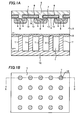
- Fig. 1B shows a plane view of the semiconductor device of the embodiment.
- Fig. 1A shows a cross-sectional view of the semiconductor device, more specifically, a cross-sectional view of a punch-through type IGBT at line X-X in Fig. 1B. This cross-sectional view shows one unit cell only, but a number of unit cells are connected in parallel actually.
- n + -type buffer layer 2 and an n - -type drift layer 3 are formed on the front surface side of a p ++ -type semiconductor substrate (a collector layer 1) by epitaxial growth.
- the collector layer 1 and the drift layer 3 are about 150 ⁇ m and 50 ⁇ m in thickness, respectively.
- conductivity types such as p + , p and p - belong in a general conductivity type
- conductivity types such as n + , n and n - belong in another general conductivity type.
- the buffer layer 2 contains a high concentration of n-type impurity, it has a function of preventing a depletion layer from reaching the collector layer 1 from the drift layer 3. Therefore, a higher break-down voltage is achieved even with the thin drift layer 3, so that, for example, the drift layer 3 of 50 ⁇ m is satisfying even for achieving a breakdown voltage of 400V.
- the buffer layer 2 has the higher concentration of n-type impurity than the drift layer 3, holes injected from the collector layer 1 are easily recombined with electrons in the buffer layer 2. Therefore, the collector layer 1 need have a large amount of impurities in total, so that the collector layer 1 need be formed thick and have the thickness of 150 ⁇ m.
- the total amount of the impurities of the collector layer 1 also increases by increasing the impurity concentration of the collector layer 1.
- the crystallinity of the collector layer 1 is disturbed when its impurity concentration is too high, there is a limitation on increasing the total amount of the impurities only by increasing the impurity concentration. Therefore, the collector layer 1 can not be formed thinner.
- P-type base regions 4 are selectively formed in the front surface of the drift layer 3, and n + -type emitter regions 5 are selectively formed in the front surfaces of these base regions 4.
- Gate electrodes 7 are formed covering at least portions of the base regions 4 between the emitter regions 5 and the drift layer 3, with the gate oxide films 6 interposed therebetween.
- Polysilicon, polycide or the like is used as an electrode material for forming the gate electrodes 7.
- the gate electrodes 7 are surrounded by an insulation film 8, and an emitter electrode 9 is formed covering the insulation film 8 and being connected with the emitter regions 5.
- the insulation film 8 may form any other shape as long as it covers the gate electrodes 7 and has openings on the emitter regions.
- Al, Cu or the like is used as an electrode material for forming the emitter electrode 9, for example.
- a plurality of trenches T are formed penetrating through the collector layer 1 and terminating in the buffer layer 2.
- Each of the trenches T has a circle shape and is distributed uniformly in the collector layer 1 as shown in Fig. 1B.
- a collector electrode 10 is further formed filling the trenches T and covering the back surface of the collector layer 1.
- Cu, Al, polysilicon or the like is used as an electrode material for forming the collector electrode 10, for example. When polysilicon is used, in particular, this provides little difference in coefficient of thermal expansion between the collector layer 1 and the collector electrode 10, thereby enhancing the stability.
- the collector layer 1 is formed thick and has the thickness of 150 ⁇ m.
- the depths of the trenches T are still easy to control with those diameters being kept almost constant in the planar direction, independent of the depth. Therefore, the depths of the trenches T are controlled so that the trenches T terminate in the buffer layer 2.
- each of the trenches T has a large diameter and thus provides a high trench density, the area of the collector layer 1 is reduced and the total amount of the impurities of the collector layer 1 is reduced.
- the FWD does not work enough.
- the diameters and the shapes of the trenches T are easy to control, such a trade-off is easy to adjust.
- the semiconductor device of the embodiment includes three types of operation aspects, i.e., the IGBT, the MOS transistor and the FWD.
- the gate electrodes 7 turn on, i.e., when a gate voltage over a threshold is applied between the emitter electrode 9 and the gate electrodes 7 in the state where a collector voltage is applied between the emitter electrode 9 and the collector electrode 10, channel regions 12 in the base regions 4 near the gate electrodes 7 are inverted to the n-type. Then, electrons are injected from the emitter electrode 9 to the drift layer 3 through the channel regions 12. With these electrons, the collector layer 1 and the drift layer 3 are forward biased, and holes are injected from the collector layer 1 to the drift layer 3. As a result of this, the resistance of the drift layer 3 largely reduces and a collector current flows from the collector electrode 10 to the emitter electrode 9.
- the path of the former includes the collector electrode 10, the collector layer 1, the buffer layer 2, the drift layer 3, the base regions 4, and the emitter electrode 9.
- the path of the latter includes the collector electrode 10, the buffer layer 2, the drift layer 3, the base regions 4, and the emitter electrode 9 since the current flows from the collector electrode 10 to the buffer layer 2 directly without through the collector layer 1 by flowing through the collector electrode 10 in the trenches T.
- the path of the former corresponds to the function as the IGBT, and the path of the latter corresponds to the operation as the MOS transistor.
- the gate electrodes 7 are switched from on to off, i.e., when a gate voltage of only 0V or below a threshold is applied between the emitter electrode 9 and the gate electrodes 7 in the state where a collector voltage is applied between the emitter electrode 9 and the collector electrode 10, the channel regions 12 turn back to the p-type and electrons are not injected from the emitter electrode 9 to the drift layer 3. Therefore, holes are not injected from the collector layer 1 to the drift layer 3 and the resistance of the drift layer 3 becomes high, so that the collector current does not flow.
- the current path from the emitter electrode 9 to the collector electrode 10 includes a current path which does not pass through the collector layer 1.
- the base regions 4, the drift layer 3 and the buffer layer 2 function as the FWD.
- the n + -type buffer layer 2 doped with phosphorus at 1 ⁇ 10 17 /cm 2 is formed on the p ++ -type semiconductor substrate (the collector layer 1) doped with, for example, boron at 1 ⁇ 10 18 /cm 2 by epitaxial growth, to have a thickness of 10 ⁇ m.
- the n - -type drift layer 3 which has a lower concentration of impurity than the buffer layer 2 is formed on the buffer layer 2 by epitaxial growth.
- the thinner drift layer 3 is realized by the buffer layer 2 formed between the collector layer 1 and the drift layer 3, and thus the drift layer 3 is formed to have a thickness of 50 ⁇ m even for achieving a breakdown voltage of 400V, for example.
- the front surface of the drift layer 3 is thermally oxidized to form a thermal oxidation film 6a.
- a gate electrode material 7a is then deposited on the thermal oxidation film 6a.
- Polysilicon or polycide is used as the gate electrode material 7a, for example.
- a photolithography and an etching are performed to the thermal oxidation film 6a and the gate electrode material 7a to form the gate oxide films 6 and the gate electrodes 7.
- a p-type impurity such as boron or the like is then ion-implanted in the drift layer 3 using the gate electrodes 7 as a mask to form the p-type base regions 4.
- a photoresist film 11 having openings in predetermined positions on the base regions 4 is then formed, and then a high concentration of n-type impurity such as phosphorus or the like is ion-implanted in the base regions 4 and a heat treatment is performed thereto to form the n + -type emitter regions 5.
- a high concentration of p-type impurity is preferably ion-implanted in a portion to separate the emitter regions 5.
- the insulation film 8 is formed to cover the whole front surface, and then a photolithography and an etching are performed thereto to form the insulation film 8 having openings on the emitter regions 5.
- An emitter electrode material such as Al, Cu or the like is then embedded therein so as to be connected to the emitter region 5, forming the emitter electrode 9.
- a photoresist pattern is formed on the back surface of the collector layer 1, and then a dry-etching with, for example, a CF type gas or an HBr type gas is performed thereto using this photoresist pattern as a mask to form the trenches T.
- the trenches T are formed to penetrate at least through the collector layer 1 and terminate in the buffer layer 2.
- the above-described etching method is selected as appropriate depending on the depths, shapes or the like of the trenches T.
- the Bosch process is preferably selected when the thickness of the collector layer 1 is about 150 ⁇ m.
- the Bosch process vertically etches the substrate deep by alternately repeating a plasma etching process mainly using SF 6 gas and a plasma deposition process mainly using C 4 F 8 gas.
- the Bosch process may cause the inner wall surfaces of the trenches T to have a rough wavy form, and this form may cause problems in the subsequent processes.
- the rough wavy surface may also be an obstacle when the trenches T having the small diameters are filled with the electrode material, providing a difficulty in completely filling the trenches T with the electrode material.
- each of the trenches T formed by this Bosch process has an almost constant opening diameter in its depth direction. Therefore, even in the case of the thick collector layer 1, when the trenches T are formed to reach the buffer layer 2 and terminate therein, the connection of the adjacent trenches T is avoidable by control.
- the collector electrode 10 is formed to cover the back surface of the collector layer 1 and fill the trenches T.
- Cu, A1 or the like is used as a material of this collector electrode, for example.
- Polysilicon may be used as the material of the collector electrode, and in this case its coefficient of thermal expansion is almost equal to that of the collector layer 1 and thus the stability is enhanced. It may be difficult to fill the trenches T with the collector electrode 10 depending on the diameters or depths of the trenches T. In this case, another etching may be performed so as to expand the openings of the trenches T only, for example.
- the collector electrode 10 is formed in the collector layer 1 from its back surface to reach the buffer layer 2. This provides both a portion formed with the collector layer 1 between the buffer layer 2 and the collector electrode 10 and a portion not formed with the collector layer 1 therebetween. This realizes the integration of the FWD in the IGBT, independent of the thickness of the collector layer 1, so that the number of processes and components is reduced in an inverter such as a motor driver.
- the shortcut between the collector electrode 10 and the buffer layer 2 is formed by forming the trenches T in the collector layer 1. Therefore, the above structure is formed according to the etching condition of the trenches T, independent of the thickness of the collector layer 1.
- the punch-through type IGBT has the thick collector layer 1, so that the embodiment is excellently applied thereto.
- the positional relationship between the trenches T and the elements formed on the front surface of the drift layer 3 is not particularly limited. However, taking this positional relationship into account provides an optimal property for use.
- the current path when functioning as the FWD, includes the emitter electrode 9, the base regions 4, the drift layer 3, the buffer layer 2 and the collector electrode 10 in the trenches T. This means that the current path is not formed under the gate electrodes 7. Therefore, as shown in Fig.
- each of the trenches T under a region between the gate electrodes 7 where the emitter electrode 9 and the drift layer 3 are directly connected, the current path as the FWD becomes shortest, the region as the IGBT becomes larger, and the area efficiency of the semiconductor device is enhanced.
- the gate electrodes 7 are formed on the emitter regions 5, the base regions 4 and the drift layer 3.
- the MOS structure on the front side of the embodiment is not limited to this.
- the gate electrode 17 may be formed to have the trench-type structure. That is, trenches 20 are formed penetrating through the base layers 14 from the emitter regions 15 and reaching the drift layer 3, gate oxide films 16 are formed on the inner sidewalls of these trenches 20, and the gate electrodes 17 are embedded in the trenches 20. With this structure, portions of the base layers 14 near the gate electrodes 17 serve as the channel regions 12.
- the insulation film 18 is formed on the gate electrodes 17, and the emitter electrode 19 covers the front surface, being connected with the emitter regions 15.
- the trenches T may be formed independent of the structure on the front surface, but the area efficiency is enhanced by forming the trenches T in relation to the structure on the front surface. For example, when each of the trenches T is formed under a portion between the gate electrodes 17 where the emitter electrode 19 and the base layer 14 are directly connected, the current path as the FWD becomes shortest, the region as the IGBT becomes larger, and the area efficiency of the semiconductor device is enhanced.
- the above description of the semiconductor device and the method of manufacturing the semiconductor device of the embodiment is given for the IGBT formed with the buffer layer 2.
- the invention is not limited to this, and may be applied to the non-punch-through type IGBT, for example, as shown in Fig. 9.
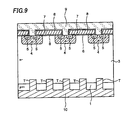
- the trenches T are formed penetrating through the collector layer 1 and terminating in the drift layer 3.
- the collector electrode 10 covering the collector layer 1 and the inside of the trenches T, the current path which does not pass through the collector layer 1 is formed and this path functions as the FWD in the similar manner to the embodiment described above.
- the trenches T are formed by an anisotropic etching.
- the invention is not limited to this.
- an isotropic etching may be used for forming openings reaching the buffer layer 2.
- the collector electrode 10 fills the trenches T.
- the invention is not limited to this, and the collector electrode 10 may be formed thin along the collector layer 1 and the trenches T.
- each of the trenches T has a circle shape and is distributed uniformly in the collector layer 1 as shown in Fig. 1B.
- the shape of the trenches T is not limited to the circle as long as they are distributed relatively uniformly in the collector layer 1.
- the trenches T may have lattice shape as shown in Fig. 12.
Landscapes
- Electrodes Of Semiconductors (AREA)
- Power Conversion In General (AREA)
Abstract
Description
- This application claims priority from
Japanese Patent Application No. 2006-298524 - The invention relates to a semiconductor device and a method of manufacturing the same, particularly, a semiconductor device having an insulated gate bipolar transistor (IGBT) and a method of manufacturing the same.
- An insulated gate bipolar transistor is called IGBT, in which a fundamental cell combines the bipolar transistor and the MOS transistor, forming a semiconductor device having both low on-voltage characteristics of the former and voltage drive characteristics of the latter.
- Fig. 10 shows a conventional semiconductor device, more specifically, a cross-sectional view of a punch-through type IGBT. This cross-sectional view shows one unit cell only, but a number of unit cells are connected in parallel actually.
- First, the structure of the conventional semiconductor device will be described. An n+-
type buffer layer 102 and an n--type drift layer 103 are formed on the front surface side of a p++-type semiconductor substrate (a collector layer 101) by epitaxial growth. P-type base regions 104 are selectively formed in the front surface of thedrift layer 103, and n+-type emitter regions 105 are selectively formed in the front surface of thebase regions 104.Gate electrodes 107 are further formed covering the front surfaces of thebase regions 104 at least in regions between theemitter regions 105 and thedrift layer 103, withgate oxide films 106 interposed therebetween. Furthermore, thegate electrodes 107 are surrounded by aninsulation film 108, and anemitter electrode 109 is formed covering theinsulation film 108 and being connected with theemitter regions 105. On the other hand, acollector electrode 110 is formed on the back surface side of thecollector layer 101. Thegate electrodes 107, theemitter electrode 109 and thecollector electrode 110 are electrically connected among all the unit cells, respectively. - Next, the operation of the conventional semiconductor device will be described. When a gate voltage over a threshold is applied between the
emitter electrode 109 and thegate electrodes 107 in the state where a collector voltage is applied between theemitter electrode 109 and thecollector electrode 110, channel regions in thebase regions 104 adjacent to thegate electrodes 107 are inverted into the n-type. Then, electrons are injected from theemitter electrode 109 to thedrift layer 103 through the channel regions. - With these electrons, the
collector layer 101 and thedrift layer 103 are forward biased, and holes are injected from thecollector layer 101 to thedrift layer 103. As a result of this, the resistance of thedrift layer 103 is largely reduced, and a collector current flowing from thecollector electrode 110 to theemitter electrode 109 reaches a high value. - The
buffer layer 102 also has a function of preventing punch-through. In detail, without thebuffer layer 102, a depletion layer expanding from thebase regions 104 reaches thecollector layer 101 when a collector voltage exceeds a breakdown voltage, and thus a collector current inadvertently flows even when a gate voltage is not applied. In this respect, when thebuffer layer 102 is provided, the expansion of the depletion layer slows down in thebuffer layer 102 and is prevented from reaching thecollector layer 101. This realizes a higher breakdown voltage even with thethinner collector layer 101, and the turn-off loss is also minimized. - Furthermore, the
buffer layer 102 has a function of minimizing the amount of the holes injected from thecollector layer 101. That is, thebuffer layer 102 has a high concentration of n-type impurity, and the holes injected from thecollector layer 101 are easily recombined with the electrons in thebuffer layer 102. Therefore, the on-resistance and the collector current are adjusted with the thickness and the impurity concentration of thebuffer layer 102. The relevant technology is described in theJapanese Patent Application Publication No. 2001-160559 - The IGBT is used as a switching element in an inverter circuit for driving a load such as a motor. Fig. 11 shows a circuit diagram of an inverter circuit for driving a motor.
- For example, when the IGBTa and the IGBTd turn on and a direct current voltage is applied to a motor load M, a current flows while accumulating and increasing an energy in the motor load M. After that, when the IGBTa and the IGBTd turn off, a current is discharged from the motor load M. At this time, if the energy accumulated in the motor load M is discharged for an instant, this current is extremely large and thus the IGBTs are broken.
- For solving this, in the inverter circuit, a free wheeling diode (hereafter, referred to as FWD) is reversely and in parallel connected to each of the IGBTs. Therefore, when the IGBTa and the IGBTd turn off, a current flows back from the motor load M, taking a detour through the FWDb and the FNDc reversely and in parallel connected to the IGBTb and the IGBTc. In detail, even when the IGBTa and the IGBTd turn off, a current flowing in the motor load M is not blocked suddenly, so that the energy accumulated in the motor load M is slowly discharged and the IGBTs are not broken.
- Accordingly, it is necessary in the inverter circuit to connect the FWD to each of the IGBTs reversely and in parallel. However, in the IGBT, the p++-
type collector layer 101 is formed on the whole back surface. This means the FWD is not integrated in the IGBT structurally, but a forward diode including the p++-type collector layer 101 and the n+-type buffer layer 102 is rather integrated therein. - Therefore, in the inverter circuit, the IGBT and the FWD need be configured of separate elements, and these elements are reversely and in parallel connected on a substrate in a package. This causes a large number of processes and components and a difficulty in reducing the cost.
- It is an object of this invention to provide an improved semiconductor and manufacturing method thereof that lessens this drawback.
- The solution according to the invention resides in the features of the independent claims and preferably in those of the dependent claims.
- The invention provides a semiconductor device including: a collector layer of a first conductivity type; a drift layer of a second conductivity type formed on a front surface of the collector layer; a first conductive type base region selectively formed in a front surface of the drift layer; a emitter region of the second conductive type selectively formed in a surface of the base region; a gate insulation film formed on the base region and covering a region of the base region between the drift layer and the emitter region; a gate electrode formed on the gate insulation film; and an emitter electrode connected with the emitter region; wherein a collector electrode is disposed on a back surface of the collector layer and comprises branching portions penetrating through the collector layer.
- The invention also provides a semiconductor device including: a collector layer of a first conductivity type; a drift layer of a second conductivity type formed on a front surface of the collector layer; a first conductive type base layer selectively formed in a surface of the drift layer; a gate insulation film formed on an inner sidewall of a trench; the trench being formed from a front surface of the base layer and reaching the drift layer; a gate electrode formed in the trench with the gate insulation film interposed therebetween; an emitter region formed in the base layer and adjacent to the trench; and an emitter electrode connected with the emitter region; wherein a collector electrode is disposed on a back surface of the collector layer and comprises branching portions penetrating through the collector layer.
- The invention also provides a method of manufacturing a semiconductor device, including: providing a semiconductor substrate having a collector layer of a first conductivity type, a drift layer of a second conductivity type formed on a front surface of the collector layer, a first conductive type base region selectively formed in a front surface of the drift layer, a emitter region of the second conductive type selectively formed in a surface of the base region, a gate insulation film formed on the base region and covering a region of the base region between the drift layer and the emitter region, a gate electrode formed on the gate insulation film, and an emitter electrode connected with the emitter region; forming openings from a back surface of the collector layer so that the openings penetrate through the collector layer; and forming a collector electrode on the back surface of the collector layer so as to fill the openings at least partially.
- The invention also provides a method of manufacturing a semiconductor device, including: providing a semiconductor substrate having a collector layer of a first conductivity type, a drift layer of a second conductivity type formed on a front surface of the collector layer, a first conductive type base layer selectively formed in a surface of the drift layer, a gate insulation film formed on an inner sidewall of a trench; the trench being formed from a front surface of the base layer and reaching the drift layer, a gate electrode formed in the trench with the gate insulation film interposed therebetween, an emitter region formed in the base layer and adjacent to the trench, and an emitter electrode connected with the emitter region; forming openings from a back surface of the collector layer so that the openings penetrate through the collector layer; and forming a collector electrode on the back surface of the collector layer so as to fill the openings at least partially.
- In the semiconductor device of the embodiment, the collector electrode is formed in the collector layer from its back surface to reach the buffer layer. This provides both a portion formed with the collector layer between the buffer layer and the collector electrode and a portion not formed with the collector layer therebetween. This realizes the integration of the FWD in the IGBT, independent of the thickness of the collector layer, and thus the number of processes and components is reduced in an inverter such as a motor driver.
- In the method of manufacturing the semiconductor device of the embodiment, the formation of the trenches in the collector layer provides a shortcut between the collector electrode and the buffer layer. Therefore, the above structure is formed according to the etching condition of the trenches, impendent of the thickness of the collector layer. Since the punch-through type IGBT particularly has a thick collector layer, the embodiment is applied thereto excellently.
-
- Fig. 1A shows a cross-sectional view of a semiconductor device of an embodiment the invention.
- Fig. 1B shows a plane view of a semiconductor device of the embodiment.
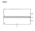
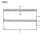
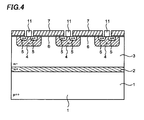
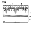
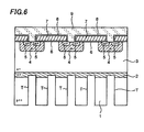
- Figs. 2 to 6 show cross-sectional views of processes of manufacturing the semiconductor device of the embodiment.
- Figs. 7 to 9 show cross-sectional views of the semiconductor device of the embodiment.
- Fig. 10 shows a cross-sectional view of a conventional semiconductor device.
- Fig. 11 shows an inverter circuit for driving a motor load.
- Fig. 12 shows a plane view of a semiconductor device of another embodiment of the invention.
- A semiconductor device of an embodiment of this invention and a method of manufacturing that device will be described in detail referring to figures.
- First, a structure of the semiconductor device of the embodiment will be described. Fig. 1B shows a plane view of the semiconductor device of the embodiment. Fig. 1A shows a cross-sectional view of the semiconductor device, more specifically, a cross-sectional view of a punch-through type IGBT at line X-X in Fig. 1B. This cross-sectional view shows one unit cell only, but a number of unit cells are connected in parallel actually.
- An n+-
type buffer layer 2 and an n--type drift layer 3 are formed on the front surface side of a p++-type semiconductor substrate (a collector layer 1) by epitaxial growth. Thecollector layer 1 and thedrift layer 3 are about 150 µm and 50 µm in thickness, respectively. - It is noted that conductivity types such as p+, p and p- belong in a general conductivity type, and conductivity types such as n+, n and n- belong in another general conductivity type.
- Since the
buffer layer 2 contains a high concentration of n-type impurity, it has a function of preventing a depletion layer from reaching thecollector layer 1 from thedrift layer 3. Therefore, a higher break-down voltage is achieved even with thethin drift layer 3, so that, for example, thedrift layer 3 of 50 µm is satisfying even for achieving a breakdown voltage of 400V. However, since thebuffer layer 2 has the higher concentration of n-type impurity than thedrift layer 3, holes injected from thecollector layer 1 are easily recombined with electrons in thebuffer layer 2. Therefore, thecollector layer 1 need have a large amount of impurities in total, so that thecollector layer 1 need be formed thick and have the thickness of 150 µm. - It is noted that the total amount of the impurities of the
collector layer 1 also increases by increasing the impurity concentration of thecollector layer 1. However, since the crystallinity of thecollector layer 1 is disturbed when its impurity concentration is too high, there is a limitation on increasing the total amount of the impurities only by increasing the impurity concentration. Therefore, thecollector layer 1 can not be formed thinner. - P-
type base regions 4 are selectively formed in the front surface of thedrift layer 3, and n+-type emitter regions 5 are selectively formed in the front surfaces of thesebase regions 4.Gate electrodes 7 are formed covering at least portions of thebase regions 4 between theemitter regions 5 and thedrift layer 3, with thegate oxide films 6 interposed therebetween. Polysilicon, polycide or the like is used as an electrode material for forming thegate electrodes 7. Thegate electrodes 7 are surrounded by aninsulation film 8, and anemitter electrode 9 is formed covering theinsulation film 8 and being connected with theemitter regions 5. Theinsulation film 8 may form any other shape as long as it covers thegate electrodes 7 and has openings on the emitter regions. Al, Cu or the like is used as an electrode material for forming theemitter electrode 9, for example. On the other hand, on the back surface side of thecollector layer 1, a plurality of trenches T are formed penetrating through thecollector layer 1 and terminating in thebuffer layer 2. Each of the trenches T has a circle shape and is distributed uniformly in thecollector layer 1 as shown in Fig. 1B. Acollector electrode 10 is further formed filling the trenches T and covering the back surface of thecollector layer 1. Cu, Al, polysilicon or the like is used as an electrode material for forming thecollector electrode 10, for example. When polysilicon is used, in particular, this provides little difference in coefficient of thermal expansion between thecollector layer 1 and thecollector electrode 10, thereby enhancing the stability. - As described above, the
collector layer 1 is formed thick and has the thickness of 150 µm. In this respect, the depths of the trenches T are still easy to control with those diameters being kept almost constant in the planar direction, independent of the depth. Therefore, the depths of the trenches T are controlled so that the trenches T terminate in thebuffer layer 2. - When each of the trenches T has a large diameter and thus provides a high trench density, the area of the
collector layer 1 is reduced and the total amount of the impurities of thecollector layer 1 is reduced. On the other hand, when each of the trenches T has a small diameter and thus provides a low trench density, the FWD does not work enough. However, since the diameters and the shapes of the trenches T are easy to control, such a trade-off is easy to adjust. - Next, an operation of the semiconductor device of the embodiment will be described. As shown in Fig. 1, the semiconductor device of the embodiment includes three types of operation aspects, i.e., the IGBT, the MOS transistor and the FWD.
- In detail, when the
gate electrodes 7 turn on, there occur two types of current paths through thecollector layer 1 and through thecollector electrode 10 in the trenches T, respectively. The former contributes to the operation as the IGBT, and the latter contributes to the operation as the MOS transistor. When thegate electrodes 7 turn off, on the contrary, there occurs only one current path through thecollector electrode 10 in the trenches T, which contributes to the operation as the FWD. - In detail, when the
gate electrodes 7 turn on, i.e., when a gate voltage over a threshold is applied between theemitter electrode 9 and thegate electrodes 7 in the state where a collector voltage is applied between theemitter electrode 9 and thecollector electrode 10,channel regions 12 in thebase regions 4 near thegate electrodes 7 are inverted to the n-type. Then, electrons are injected from theemitter electrode 9 to thedrift layer 3 through thechannel regions 12. With these electrons, thecollector layer 1 and thedrift layer 3 are forward biased, and holes are injected from thecollector layer 1 to thedrift layer 3. As a result of this, the resistance of thedrift layer 3 largely reduces and a collector current flows from thecollector electrode 10 to theemitter electrode 9. - At this time, in the semiconductor device of the embodiment, there are two types of current paths of the collector current; one that passes through the
collector layer 1 and another that does not pass through thecollector layer 1. - That is, the path of the former includes the
collector electrode 10, thecollector layer 1, thebuffer layer 2, thedrift layer 3, thebase regions 4, and theemitter electrode 9. The path of the latter includes thecollector electrode 10, thebuffer layer 2, thedrift layer 3, thebase regions 4, and theemitter electrode 9 since the current flows from thecollector electrode 10 to thebuffer layer 2 directly without through thecollector layer 1 by flowing through thecollector electrode 10 in the trenches T. The path of the former corresponds to the function as the IGBT, and the path of the latter corresponds to the operation as the MOS transistor. - On the contrary, when the
gate electrodes 7 are switched from on to off, i.e., when a gate voltage of only 0V or below a threshold is applied between theemitter electrode 9 and thegate electrodes 7 in the state where a collector voltage is applied between theemitter electrode 9 and thecollector electrode 10, thechannel regions 12 turn back to the p-type and electrons are not injected from theemitter electrode 9 to thedrift layer 3. Therefore, holes are not injected from thecollector layer 1 to thedrift layer 3 and the resistance of thedrift layer 3 becomes high, so that the collector current does not flow. In such a state, when a voltage is applied between theemitter electrode 9 and thecollector electrode 10 by, for example, a motor load connected to outside, a forward current flows through theemitter electrode 9, thebase regions 4, thedrift layer 3, thebuffer layer 2, and thecollector electrode 10 in the trenches T. That is, in the semiconductor device of this embodiment, since the trenches T penetrate through thecollector layer 1 to reach thebuffer layer 2 and thecollector electrode 10 is formed in these trenches T, too, the current path from theemitter electrode 9 to thecollector electrode 10 includes a current path which does not pass through thecollector layer 1. In this current path, thebase regions 4, thedrift layer 3 and thebuffer layer 2 function as the FWD. - In the semiconductor device of this embodiment, even when a large collector voltage is applied when the
gate electrode 7 is turned off, the expansion of a depletion layer from thebase region 4 is controlled by thebuffer layer 2 and prevented from reaching thecollector layer 1. Therefore, even with thethin drift layer 3, a depletion layer expanding from thebase region 4 does not easily reach thecollector layer 1, thereby achieving a higher breakdown voltage. - Next, a description will be given on a method of manufacturing the semiconductor device of the embodiment.
- First, as shown in Fig. 2, the n+-
type buffer layer 2 doped with phosphorus at 1×10¹⁷/cm2 is formed on the p++-type semiconductor substrate (the collector layer 1) doped with, for example, boron at 1×10¹⁸/cm2 by epitaxial growth, to have a thickness of 10 µm. The n--type drift layer 3 which has a lower concentration of impurity than thebuffer layer 2 is formed on thebuffer layer 2 by epitaxial growth. In the semiconductor device of the embodiment, thethinner drift layer 3 is realized by thebuffer layer 2 formed between thecollector layer 1 and thedrift layer 3, and thus thedrift layer 3 is formed to have a thickness of 50 µm even for achieving a breakdown voltage of 400V, for example. - Then, as shown in Fig. 3, the front surface of the
drift layer 3 is thermally oxidized to form athermal oxidation film 6a. Agate electrode material 7a is then deposited on thethermal oxidation film 6a. Polysilicon or polycide is used as thegate electrode material 7a, for example. - Then, as shown in Fig. 4, a photolithography and an etching are performed to the
thermal oxidation film 6a and thegate electrode material 7a to form thegate oxide films 6 and thegate electrodes 7. A p-type impurity such as boron or the like is then ion-implanted in thedrift layer 3 using thegate electrodes 7 as a mask to form the p-type base regions 4. Aphotoresist film 11 having openings in predetermined positions on thebase regions 4 is then formed, and then a high concentration of n-type impurity such as phosphorus or the like is ion-implanted in thebase regions 4 and a heat treatment is performed thereto to form the n+-type emitter regions 5. When theadjacent emitter regions 5 are connected to each other by the heat treatment, a high concentration of p-type impurity is preferably ion-implanted in a portion to separate theemitter regions 5. - Then, as shown in Fig. 5, the
insulation film 8 is formed to cover the whole front surface, and then a photolithography and an etching are performed thereto to form theinsulation film 8 having openings on theemitter regions 5. An emitter electrode material such as Al, Cu or the like is then embedded therein so as to be connected to theemitter region 5, forming theemitter electrode 9. - Then, as shown in Fig. 6, a photoresist pattern is formed on the back surface of the
collector layer 1, and then a dry-etching with, for example, a CF type gas or an HBr type gas is performed thereto using this photoresist pattern as a mask to form the trenches T. The trenches T are formed to penetrate at least through thecollector layer 1 and terminate in thebuffer layer 2. - The above-described etching method is selected as appropriate depending on the depths, shapes or the like of the trenches T. For example, the Bosch process is preferably selected when the thickness of the
collector layer 1 is about 150 µm. The Bosch process vertically etches the substrate deep by alternately repeating a plasma etching process mainly using SF6 gas and a plasma deposition process mainly using C4F8 gas. However, the Bosch process may cause the inner wall surfaces of the trenches T to have a rough wavy form, and this form may cause problems in the subsequent processes. For example, the rough wavy surface may also be an obstacle when the trenches T having the small diameters are filled with the electrode material, providing a difficulty in completely filling the trenches T with the electrode material. For solving these problems, it is preferable to further perform a dry-etching after the Bosch process to planarize the inner walls of the trenches T, for example. Each of the trenches T formed by this Bosch process has an almost constant opening diameter in its depth direction. Therefore, even in the case of thethick collector layer 1, when the trenches T are formed to reach thebuffer layer 2 and terminate therein, the connection of the adjacent trenches T is avoidable by control. - Then, as shown in Fig. 1, the
collector electrode 10 is formed to cover the back surface of thecollector layer 1 and fill the trenches T. Cu, A1 or the like is used as a material of this collector electrode, for example. - Polysilicon may be used as the material of the collector electrode, and in this case its coefficient of thermal expansion is almost equal to that of the
collector layer 1 and thus the stability is enhanced. It may be difficult to fill the trenches T with thecollector electrode 10 depending on the diameters or depths of the trenches T. In this case, another etching may be performed so as to expand the openings of the trenches T only, for example. - The semiconductor device and the method of manufacturing the semiconductor device of the embodiment are thus described above in detail referring to figures.
- In the semiconductor device of the embodiment, the
collector electrode 10 is formed in thecollector layer 1 from its back surface to reach thebuffer layer 2. This provides both a portion formed with thecollector layer 1 between thebuffer layer 2 and thecollector electrode 10 and a portion not formed with thecollector layer 1 therebetween. This realizes the integration of the FWD in the IGBT, independent of the thickness of thecollector layer 1, so that the number of processes and components is reduced in an inverter such as a motor driver. - In the method of manufacturing the semiconductor device of the embodiment, the shortcut between the
collector electrode 10 and thebuffer layer 2 is formed by forming the trenches T in thecollector layer 1. Therefore, the above structure is formed according to the etching condition of the trenches T, independent of the thickness of thecollector layer 1. In particular, the punch-through type IGBT has thethick collector layer 1, so that the embodiment is excellently applied thereto. - The embodiments disclosed herein are exemplary in all aspects and do not limit the scope of this invention.
- For example, in the above description of the semiconductor device and the method of manufacturing the semiconductor device of the embodiment, the positional relationship between the trenches T and the elements formed on the front surface of the
drift layer 3 is not particularly limited. However, taking this positional relationship into account provides an optimal property for use. For example, when functioning as the FWD, the current path includes theemitter electrode 9, thebase regions 4, thedrift layer 3, thebuffer layer 2 and thecollector electrode 10 in the trenches T. This means that the current path is not formed under thegate electrodes 7. Therefore, as shown in Fig. 7, by forming each of the trenches T under a region between thegate electrodes 7 where theemitter electrode 9 and thedrift layer 3 are directly connected, the current path as the FWD becomes shortest, the region as the IGBT becomes larger, and the area efficiency of the semiconductor device is enhanced. - Furthermore, in the above description of the semiconductor device and the method of manufacturing the semiconductor device of the embodiment, the
gate electrodes 7 are formed on theemitter regions 5, thebase regions 4 and thedrift layer 3. However, the MOS structure on the front side of the embodiment is not limited to this. For example, as shown in Fig. 8, thegate electrode 17 may be formed to have the trench-type structure. That is,trenches 20 are formed penetrating through the base layers 14 from theemitter regions 15 and reaching thedrift layer 3,gate oxide films 16 are formed on the inner sidewalls of thesetrenches 20, and thegate electrodes 17 are embedded in thetrenches 20. With this structure, portions of the base layers 14 near thegate electrodes 17 serve as thechannel regions 12. Theinsulation film 18 is formed on thegate electrodes 17, and theemitter electrode 19 covers the front surface, being connected with theemitter regions 15. In this structure, too, the trenches T may be formed independent of the structure on the front surface, but the area efficiency is enhanced by forming the trenches T in relation to the structure on the front surface. For example, when each of the trenches T is formed under a portion between thegate electrodes 17 where theemitter electrode 19 and thebase layer 14 are directly connected, the current path as the FWD becomes shortest, the region as the IGBT becomes larger, and the area efficiency of the semiconductor device is enhanced. - Furthermore, the above description of the semiconductor device and the method of manufacturing the semiconductor device of the embodiment is given for the IGBT formed with the
buffer layer 2. However, the invention is not limited to this, and may be applied to the non-punch-through type IGBT, for example, as shown in Fig. 9. In this case, the trenches T are formed penetrating through thecollector layer 1 and terminating in thedrift layer 3. Furthermore, by forming thecollector electrode 10 covering thecollector layer 1 and the inside of the trenches T, the current path which does not pass through thecollector layer 1 is formed and this path functions as the FWD in the similar manner to the embodiment described above. - In the above description of the semiconductor device and the method of manufacturing the semiconductor device of the embodiment, the trenches T are formed by an anisotropic etching. However, the invention is not limited to this. For example, when the
collector layer 1 is thin, an isotropic etching may be used for forming openings reaching thebuffer layer 2. - Furthermore, in the above description of the semiconductor device and the method of manufacturing the semiconductor device of the embodiment, the
collector electrode 10 fills the trenches T. However, the invention is not limited to this, and thecollector electrode 10 may be formed thin along thecollector layer 1 and the trenches T. - Furthermore, in the embodiment, each of the trenches T has a circle shape and is distributed uniformly in the
collector layer 1 as shown in Fig. 1B. However, the shape of the trenches T is not limited to the circle as long as they are distributed relatively uniformly in thecollector layer 1. For example, the trenches T may have lattice shape as shown in Fig. 12.
Claims (22)
- A semiconductor device comprising:a collector layer (1) of a first general conductivity type;a drift layer (3) of a second general conductivity type disposed on a front surface of the collector layer (1);a base region (4) of the first general conductivity type formed in the drift layer (3);an emitter region (5) of the second general conductivity type formed in the base region (4);a gate insulation film (6) disposed on the base region (4) so as to cover a portion of the base region (4) between the drift layer (3) and the emitter region (5);a gate electrode (7) disposed on the gate insulation film (6);an emitter electrode (9) connected to the emitter region (5); anda collector electrode (10) disposed on a back surface of the collector layer (1) and comprising branching portions penetrating through the collector layer.
- The semiconductor device of claim 1, further comprising a buffer layer (2) of the second general conductivity type disposed between the collector layer (1) and the drift layer (3) and having a higher impurity concentration than the drift layer (3).
- The semiconductor device of claim 2, wherein the branching portions terminate in the buffer layer (2).
- The semiconductor device according to any of claims 1 to 3, wherein the branching portions are formed as trenches (T).
- The semiconductor device of claim 4, wherein the collector electrode fills the trenches.
- The semiconductor device according to any of claims 1 to 5, wherein the branching portions comprise tapered sidewalls.
- The semiconductor device according to any of claims 1 to 6, wherein the collector electrode (10) comprises copper.
- The semiconductor device according to any of claims 1 to 6, wherein the collector electrode (10) comprises polysilicon.
- The semiconductor device of claim 1, wherein one of the branching portions is disposed under the base region (4) between the gate electrode (7) and another gate electrode (7).
- A semiconductor device comprising:a collector layer (1) of a first general conductivity type;a drift layer (3) of a second general conductivity type disposed on a front surface of the collector layer (1);a base layer (14) of the first general conductivity type disposed on the drift layer (3);a trench (20) penetrating through the base layer so as to reach the drift layer (3);a gate insulation film (16) disposed on an inner wall of the trench (20);a gate electrode (17) disposed in the trench (20) so as to cover the gate insulation film (16);an emitter region (15) of the second general conductivity type formed in the base layer (14) and adjacent the trench (20);an emitter electrode (19) connected to the emitter region (15); anda collector electrode (10) disposed on a back surface of the collector layer (1) and comprising branching portions penetrating through the collector layer (1).
- The semiconductor device of claim 10, further comprising a buffer layer (2) of the second general conductivity type disposed between the collector layer (1) and the drift layer (3) and having a higher impurity concentration than the drift layer (3).
- The semiconductor device of claim 11, wherein the branching portions terminate in the buffer layer (2).
- The semiconductor device according to any of claims 10 to 12, wherein the branching portions are formed as trenches (T).
- The semiconductor device of claim 13, wherein the collector electrode (1) fills the trenches (T).
- The semiconductor device according to any of claims 10 to 14, wherein the branching portions comprise tapered sidewalls.
- The semiconductor device according to any of claims 10 to 15, wherein the collector electrode (10) comprises copper.
- The semiconductor device according to any of claims 10 to 15, wherein the collector electrode (10) comprises polysilicon. '
- The semiconductor device according to any of claims 10 to 17, wherein one of the branching portions is disposed under the base layer (14) between the gate electrode (17) and another gate electrode (17).
- A method of manufacturing a semiconductor device, comprising:providing a collector layer (1) of a first general conductivity type;forming a drift layer (3) of a second general conductivity type on a front surface of the collector layer (1) ;forming base regions (4) of the first general conductivity type in the drift layer (3);forming emitter regions (5) of the second general conductivity type in the base regions (4);forming a gate insulation film (6) on the base regions (4) so as to cover portions of the base regions (4) between the drift layer (3) and the emitter regions (5);forming gate electrodes (7) on the gate insulation film (6);forming an emitter electrode (9) so as to be connected to the emitter regions (5);forming openings from a back surface of the collector layer (1) so that the openings penetrate through the collector layer (1); andforming a collector electrode (10) on the back surface of the collector layer (1) so as to fill the openings at least partially.
- The method of claim 19, wherein the openings are formed under base regions (4) between the gate electrodes (7).
- A method of manufacturing a semiconductor device, comprising:providing a collector layer (1) of a first general conductivity type;forming a drift layer (3) of a second general conductivity type on a front surface of the collector layer (1) ;forming a base layer (14) of the first general conductivity type on the drift layer (3);forming trenches (20) penetrating through the base layer (14) so as to reach the drift layer (3);forming a gate insulation film (16) on an inner wall of each of the trenches (20);forming a gate electrode (17) in each of the trenches so as to cover a corresponding gate insulation film (16);forming emitter regions (15) of the second general conductivity type in the base layer (14) and adjacent the trenches (20);forming an emitter electrode (19) connected to the emitter regions (15);forming openings from a back surface of the collector layer (1) so that the openings penetrate through the collector layer (1); andforming a collector electrode (10) on the back surface of the collector layer (1) so as to fill the openings at least partially.
- The method of claim 21, wherein the openings are formed under the base layer (14) between the gate electrodes (17).
Applications Claiming Priority (1)
| Application Number | Priority Date | Filing Date | Title |
|---|---|---|---|
| JP2006298524A JP2008117881A (en) | 2006-11-02 | 2006-11-02 | Semiconductor device and manufacturing method thereof |
Publications (2)
| Publication Number | Publication Date |
|---|---|
| EP1918980A2 true EP1918980A2 (en) | 2008-05-07 |
| EP1918980A3 EP1918980A3 (en) | 2008-07-09 |
Family
ID=39263269
Family Applications (1)
| Application Number | Title | Priority Date | Filing Date |
|---|---|---|---|
| EP07021414A Withdrawn EP1918980A3 (en) | 2006-11-02 | 2007-11-02 | Semiconductor device and method of manufacturing the same |
Country Status (4)
| Country | Link |
|---|---|
| US (1) | US7659576B2 (en) |
| EP (1) | EP1918980A3 (en) |
| JP (1) | JP2008117881A (en) |
| KR (1) | KR20080040610A (en) |
Cited By (3)
| Publication number | Priority date | Publication date | Assignee | Title |
|---|---|---|---|---|
| CN103703566A (en) * | 2011-08-02 | 2014-04-02 | 罗姆股份有限公司 | Semiconductor device, and manufacturing method for same |
| CN106057876A (en) * | 2016-07-19 | 2016-10-26 | 上海华虹宏力半导体制造有限公司 | IGBT with reverse freewheeling capacity and manufacturing method thereof |
| CN108417614A (en) * | 2017-02-09 | 2018-08-17 | 株式会社东芝 | Semiconductor device |
Families Citing this family (29)
| Publication number | Priority date | Publication date | Assignee | Title |
|---|---|---|---|---|
| JP5332376B2 (en) * | 2008-07-28 | 2013-11-06 | 富士電機株式会社 | Semiconductor device and manufacturing method thereof |
| JP5333342B2 (en) * | 2009-06-29 | 2013-11-06 | 株式会社デンソー | Semiconductor device |
| JP5526811B2 (en) | 2010-01-29 | 2014-06-18 | 富士電機株式会社 | Reverse conducting insulated gate bipolar transistor |
| KR101136782B1 (en) * | 2010-05-20 | 2012-04-19 | (주) 트리노테크놀로지 | super-junction power semiconductor device |
| JP5361808B2 (en) | 2010-06-23 | 2013-12-04 | 三菱電機株式会社 | Power semiconductor device |
| JP5811829B2 (en) | 2011-12-22 | 2015-11-11 | 住友電気工業株式会社 | Manufacturing method of semiconductor device |
| CN103035691B (en) * | 2012-03-12 | 2015-08-19 | 上海华虹宏力半导体制造有限公司 | Inverse conductivity type IGBT semiconductor device and manufacture method thereof |
| CN103022099B (en) * | 2013-01-10 | 2016-05-04 | 江苏物联网研究发展中心 | A kind of IGBT collector structure and its preparation method |
| CN103972280A (en) * | 2013-01-30 | 2014-08-06 | 苏州同冠微电子有限公司 | IGBT with field stop structure and manufacturing method thereof |
| CN104253151B (en) * | 2013-06-27 | 2017-06-27 | 无锡华润上华半导体有限公司 | Field cut-off type reverse-conducting insulated gate bipolar transistor npn npn and its manufacture method |
| CN104253152A (en) * | 2013-06-28 | 2014-12-31 | 无锡华润上华半导体有限公司 | IGBT (insulated gate bipolar transistor) and manufacturing method thereof |
| CN104299990A (en) * | 2013-07-19 | 2015-01-21 | 无锡华润上华半导体有限公司 | IGBT (Insulated Gate Bipolar Transistor) and manufacture method thereof |
| KR101490350B1 (en) * | 2013-08-21 | 2015-02-10 | 이태복 | Apparatus and method for manufacturing a power semiconductor device |
| CN104425245B (en) | 2013-08-23 | 2017-11-07 | 无锡华润上华科技有限公司 | Reverse-conducting insulated gate bipolar transistor npn npn manufacture method |
| CN104576716B (en) * | 2013-10-24 | 2017-12-05 | 上海华虹宏力半导体制造有限公司 | The IGBT device and manufacture method of integrated super barrier rectifier |
| CN103811336B (en) * | 2014-02-21 | 2017-01-25 | 成都方舟微电子有限公司 | IGBT (Insulated Gate Bipolar Translator) power device applied at low power and manufacturing method thereof |
| TW201618299A (en) * | 2014-11-12 | 2016-05-16 | 台灣茂矽電子股份有限公司 | Power semiconductor component and method of manufacturing same |
| CN104681433B (en) * | 2015-01-26 | 2017-07-11 | 电子科技大学 | A kind of FS IGBT preparation method |
| CN106298693A (en) * | 2015-05-13 | 2017-01-04 | 国网智能电网研究院 | A kind of manufacture method of high-voltage chip passivation layer |
| CN105161529B (en) * | 2015-08-21 | 2018-05-18 | 中国东方电气集团有限公司 | Field blanking voltage control type power device with adaptivity |
| CN105870194A (en) * | 2016-05-31 | 2016-08-17 | 苏州同冠微电子有限公司 | Groove type CoolMOS and manufacturing method thereof |
| WO2018012510A1 (en) * | 2016-07-15 | 2018-01-18 | ローム株式会社 | Semiconductor device and method for manufacturing semiconductor device |
| CN106024875B (en) * | 2016-07-19 | 2019-02-05 | 东南大学 | A fast turn-off silicon-on-insulator lateral insulated gate bipolar transistor device |
| US11233141B2 (en) | 2018-01-16 | 2022-01-25 | Ipower Semiconductor | Self-aligned and robust IGBT devices |
| WO2019157222A1 (en) * | 2018-02-07 | 2019-08-15 | Ipower Semiconductor | Igbt devices with 3d backside structures for field stop and reverse conduction |
| US11411099B2 (en) * | 2019-05-28 | 2022-08-09 | Glc Semiconductor Group (Cq) Co., Ltd. | Semiconductor device |
| US12457759B2 (en) * | 2021-07-23 | 2025-10-28 | Taiwan Semiconductor Manufacturing Company Limited | Semiconductor arrangement and method of manufacture |
| CN116666210A (en) * | 2022-02-21 | 2023-08-29 | 珠海零边界集成电路有限公司 | Insulated gate bipolar transistor, manufacturing method, electronic device, and storage medium |
| CN116259541B (en) * | 2022-12-21 | 2026-05-26 | 天狼芯半导体(成都)有限公司 | A novel gallium nitride IGBT device and its fabrication method and chip |
Citations (2)
| Publication number | Priority date | Publication date | Assignee | Title |
|---|---|---|---|---|
| JP2001160559A (en) | 1999-12-01 | 2001-06-12 | Fuji Electric Co Ltd | Method for manufacturing semiconductor device |
| JP2006298524A (en) | 2005-04-18 | 2006-11-02 | Nippon Sharyo Seizo Kaisha Ltd | Telescopic boom type crawler crane |
Family Cites Families (10)
| Publication number | Priority date | Publication date | Assignee | Title |
|---|---|---|---|---|
| JPS6459947A (en) | 1987-08-31 | 1989-03-07 | Toshiba Corp | Semiconductor device |
| GB9207472D0 (en) * | 1992-04-06 | 1992-05-20 | Phoenix Vlsi Consultants Ltd | High performance process technology |
| JPH07153942A (en) * | 1993-12-01 | 1995-06-16 | Matsushita Electron Corp | Insulated gate bipolar transistor and manufacturing method thereof |
| JPH11274516A (en) | 1998-03-18 | 1999-10-08 | Toshiba Corp | Power semiconductor device |
| JP4097416B2 (en) * | 2001-10-26 | 2008-06-11 | 新電元工業株式会社 | Insulated gate bipolar transistor and manufacturing method thereof |
| US6960837B2 (en) * | 2002-02-26 | 2005-11-01 | International Business Machines Corporation | Method of connecting core I/O pins to backside chip I/O pads |
| JP2004134762A (en) * | 2002-09-19 | 2004-04-30 | Denso Corp | Semiconductor device |
| US7132321B2 (en) * | 2002-10-24 | 2006-11-07 | The United States Of America As Represented By The Secretary Of The Navy | Vertical conducting power semiconductor devices implemented by deep etch |
| US7259411B1 (en) * | 2003-12-04 | 2007-08-21 | National Semiconductor Corporation | Vertical MOS transistor |
| JP4791704B2 (en) * | 2004-04-28 | 2011-10-12 | 三菱電機株式会社 | Reverse conducting type semiconductor device and manufacturing method thereof |
-
2006
- 2006-11-02 JP JP2006298524A patent/JP2008117881A/en active Pending
-
2007
- 2007-11-01 US US11/933,897 patent/US7659576B2/en active Active
- 2007-11-02 EP EP07021414A patent/EP1918980A3/en not_active Withdrawn
- 2007-11-02 KR KR1020070111712A patent/KR20080040610A/en not_active Ceased
Patent Citations (2)
| Publication number | Priority date | Publication date | Assignee | Title |
|---|---|---|---|---|
| JP2001160559A (en) | 1999-12-01 | 2001-06-12 | Fuji Electric Co Ltd | Method for manufacturing semiconductor device |
| JP2006298524A (en) | 2005-04-18 | 2006-11-02 | Nippon Sharyo Seizo Kaisha Ltd | Telescopic boom type crawler crane |
Cited By (12)
| Publication number | Priority date | Publication date | Assignee | Title |
|---|---|---|---|---|
| CN103703566A (en) * | 2011-08-02 | 2014-04-02 | 罗姆股份有限公司 | Semiconductor device, and manufacturing method for same |
| EP2741336A4 (en) * | 2011-08-02 | 2015-03-18 | Rohm Co Ltd | SEMICONDUCTOR DEVICE AND METHOD FOR MANUFACTURING THE SAME |
| US9419117B2 (en) | 2011-08-02 | 2016-08-16 | Rohm Co., Ltd. | Semiconductor device, and manufacturing method for same |
| US9620588B2 (en) | 2011-08-02 | 2017-04-11 | Rohm Co., Ltd. | Semiconductor device |
| CN103703566B (en) * | 2011-08-02 | 2017-05-17 | 罗姆股份有限公司 | Semiconductor device, and manufacturing method for same |
| US10192865B2 (en) | 2011-08-02 | 2019-01-29 | Rohm Co., Ltd. | Method of manufacturing a semiconductor device |
| US10461077B2 (en) | 2011-08-02 | 2019-10-29 | Rohm Co., Ltd. | Method of manufacturing a semiconductor device |
| US10692861B2 (en) | 2011-08-02 | 2020-06-23 | Rohm Co., Ltd. | Method of manufacturing a semiconductor device |
| CN106057876A (en) * | 2016-07-19 | 2016-10-26 | 上海华虹宏力半导体制造有限公司 | IGBT with reverse freewheeling capacity and manufacturing method thereof |
| CN106057876B (en) * | 2016-07-19 | 2019-10-11 | 上海华虹宏力半导体制造有限公司 | IGBT with reverse freewheeling capability and manufacturing method thereof |
| CN108417614A (en) * | 2017-02-09 | 2018-08-17 | 株式会社东芝 | Semiconductor device |
| CN108417614B (en) * | 2017-02-09 | 2022-01-18 | 株式会社东芝 | Semiconductor device with a plurality of semiconductor chips |
Also Published As
| Publication number | Publication date |
|---|---|
| US7659576B2 (en) | 2010-02-09 |
| KR20080040610A (en) | 2008-05-08 |
| EP1918980A3 (en) | 2008-07-09 |
| JP2008117881A (en) | 2008-05-22 |
| US20080135870A1 (en) | 2008-06-12 |
Similar Documents
| Publication | Publication Date | Title |
|---|---|---|
| US7659576B2 (en) | Semiconductor device and method of manufacturing the same | |
| US10825906B2 (en) | Semiconductor device with transistor cells and enhancement cells with delayed control signals | |
| US7238576B2 (en) | Semiconductor device and method of manufacturing the same | |
| JP5984282B2 (en) | Vertical trench insulated gate MOS semiconductor device | |
| JP5384878B2 (en) | Semiconductor device and manufacturing method thereof | |
| US20190148369A1 (en) | Method of manufacturing a semiconductor device | |
| US20070215938A1 (en) | Semiconductor device and manufacturing method of the same | |
| JPH09139510A (en) | Semiconductor device and manufacturing method thereof | |
| JP2010153864A (en) | Power transistor device manufactured on semiconductor die | |
| JP2012059841A (en) | Semiconductor device | |
| JP5687582B2 (en) | Semiconductor device and manufacturing method thereof | |
| JPH1197715A (en) | Semiconductor device | |
| KR101968825B1 (en) | Transistor device with a field electrode including two layers | |
| US9502547B2 (en) | Charge reservoir IGBT top structure | |
| JP2006210392A (en) | Semiconductor device and manufacturing method thereof | |
| US5773851A (en) | Semiconductor device and manufacturing method thereof | |
| JP2009043782A (en) | Semiconductor device and manufacturing method thereof | |
| JP2006186108A (en) | Semiconductor device | |
| JP7330396B2 (en) | Semiconductor device and power conversion device | |
| JP2006245477A (en) | Semiconductor device | |
| US20250380440A1 (en) | Insulated gate semiconductor device | |
| EP1908116B1 (en) | Power semiconductor device | |
| JP2014154739A (en) | Semiconductor device | |
| JPH08274351A (en) | Dielectric isolation semiconductor device and manufacturing method thereof | |
| JP5261893B2 (en) | Trench type insulated gate bipolar transistor |
Legal Events
| Date | Code | Title | Description |
|---|---|---|---|
| PUAI | Public reference made under article 153(3) epc to a published international application that has entered the european phase |
Free format text: ORIGINAL CODE: 0009012 |
|
| AK | Designated contracting states |
Kind code of ref document: A2 Designated state(s): AT BE BG CH CY CZ DE DK EE ES FI FR GB GR HU IE IS IT LI LT LU LV MC MT NL PL PT RO SE SI SK TR |
|
| AX | Request for extension of the european patent |
Extension state: AL BA HR MK RS |
|
| PUAL | Search report despatched |
Free format text: ORIGINAL CODE: 0009013 |
|
| AK | Designated contracting states |
Kind code of ref document: A3 Designated state(s): AT BE BG CH CY CZ DE DK EE ES FI FR GB GR HU IE IS IT LI LT LU LV MC MT NL PL PT RO SE SI SK TR |
|
| AX | Request for extension of the european patent |
Extension state: AL BA HR MK RS |
|
| RIC1 | Information provided on ipc code assigned before grant |
Ipc: H01L 29/45 20060101ALN20080603BHEP Ipc: H01L 29/06 20060101ALN20080603BHEP Ipc: H01L 29/417 20060101ALI20080603BHEP Ipc: H01L 21/331 20060101ALI20080603BHEP Ipc: H01L 29/739 20060101ALI20080603BHEP Ipc: H01L 29/08 20060101AFI20080603BHEP |
|
| 17P | Request for examination filed |
Effective date: 20081230 |
|
| AKX | Designation fees paid |
Designated state(s): DE |
|
| STAA | Information on the status of an ep patent application or granted ep patent |
Free format text: STATUS: THE APPLICATION IS DEEMED TO BE WITHDRAWN |
|
| 18D | Application deemed to be withdrawn |
Effective date: 20150602 |