EP1918331B1 - Multi-layered magnetic pigment - Google Patents
Multi-layered magnetic pigment Download PDFInfo
- Publication number
- EP1918331B1 EP1918331B1 EP07021050.5A EP07021050A EP1918331B1 EP 1918331 B1 EP1918331 B1 EP 1918331B1 EP 07021050 A EP07021050 A EP 07021050A EP 1918331 B1 EP1918331 B1 EP 1918331B1
- Authority
- EP
- European Patent Office
- Prior art keywords
- magnetic
- layer
- dielectric
- pigment
- flake
- Prior art date
- Legal status (The legal status is an assumption and is not a legal conclusion. Google has not performed a legal analysis and makes no representation as to the accuracy of the status listed.)
- Expired - Lifetime
Links
Images


Classifications
-
- B—PERFORMING OPERATIONS; TRANSPORTING
- B32—LAYERED PRODUCTS
- B32B—LAYERED PRODUCTS, i.e. PRODUCTS BUILT-UP OF STRATA OF FLAT OR NON-FLAT, e.g. CELLULAR OR HONEYCOMB, FORM
- B32B5/00—Layered products characterised by the non- homogeneity or physical structure, i.e. comprising a fibrous, filamentary, particulate or foam layer; Layered products characterised by having a layer differing constitutionally or physically in different parts
- B32B5/16—Layered products characterised by the non- homogeneity or physical structure, i.e. comprising a fibrous, filamentary, particulate or foam layer; Layered products characterised by having a layer differing constitutionally or physically in different parts characterised by features of a layer formed of particles, e.g. chips, powder or granules
-
- B—PERFORMING OPERATIONS; TRANSPORTING
- B42—BOOKBINDING; ALBUMS; FILES; SPECIAL PRINTED MATTER
- B42D—BOOKS; BOOK COVERS; LOOSE LEAVES; PRINTED MATTER CHARACTERISED BY IDENTIFICATION OR SECURITY FEATURES; PRINTED MATTER OF SPECIAL FORMAT OR STYLE NOT OTHERWISE PROVIDED FOR; DEVICES FOR USE THEREWITH AND NOT OTHERWISE PROVIDED FOR; MOVABLE-STRIP WRITING OR READING APPARATUS
- B42D25/00—Information-bearing cards or sheet-like structures characterised by identification or security features; Manufacture thereof
- B42D25/30—Identification or security features, e.g. for preventing forgery
- B42D25/36—Identification or security features, e.g. for preventing forgery comprising special materials
- B42D25/369—Magnetised or magnetisable materials
-
- B—PERFORMING OPERATIONS; TRANSPORTING
- B41—PRINTING; LINING MACHINES; TYPEWRITERS; STAMPS
- B41M—PRINTING, DUPLICATING, MARKING, OR COPYING PROCESSES; COLOUR PRINTING
- B41M3/00—Printing processes to produce particular kinds of printed work, e.g. patterns
- B41M3/14—Security printing
-
- B—PERFORMING OPERATIONS; TRANSPORTING
- B42—BOOKBINDING; ALBUMS; FILES; SPECIAL PRINTED MATTER
- B42D—BOOKS; BOOK COVERS; LOOSE LEAVES; PRINTED MATTER CHARACTERISED BY IDENTIFICATION OR SECURITY FEATURES; PRINTED MATTER OF SPECIAL FORMAT OR STYLE NOT OTHERWISE PROVIDED FOR; DEVICES FOR USE THEREWITH AND NOT OTHERWISE PROVIDED FOR; MOVABLE-STRIP WRITING OR READING APPARATUS
- B42D25/00—Information-bearing cards or sheet-like structures characterised by identification or security features; Manufacture thereof
- B42D25/20—Information-bearing cards or sheet-like structures characterised by identification or security features; Manufacture thereof characterised by a particular use or purpose
- B42D25/29—Securities; Bank notes
-
- C—CHEMISTRY; METALLURGY
- C09—DYES; PAINTS; POLISHES; NATURAL RESINS; ADHESIVES; COMPOSITIONS NOT OTHERWISE PROVIDED FOR; APPLICATIONS OF MATERIALS NOT OTHERWISE PROVIDED FOR
- C09C—TREATMENT OF INORGANIC MATERIALS, OTHER THAN FIBROUS FILLERS, TO ENHANCE THEIR PIGMENTING OR FILLING PROPERTIES ; PREPARATION OF CARBON BLACK ; PREPARATION OF INORGANIC MATERIALS WHICH ARE NO SINGLE CHEMICAL COMPOUNDS AND WHICH ARE MAINLY USED AS PIGMENTS OR FILLERS
- C09C1/00—Treatment of specific inorganic materials other than fibrous fillers; Preparation of carbon black
- C09C1/0015—Pigments exhibiting interference colours, e.g. transparent platelets of appropriate thinness or flaky substrates, e.g. mica, bearing appropriate thin transparent coatings
-
- C—CHEMISTRY; METALLURGY
- C09—DYES; PAINTS; POLISHES; NATURAL RESINS; ADHESIVES; COMPOSITIONS NOT OTHERWISE PROVIDED FOR; APPLICATIONS OF MATERIALS NOT OTHERWISE PROVIDED FOR
- C09C—TREATMENT OF INORGANIC MATERIALS, OTHER THAN FIBROUS FILLERS, TO ENHANCE THEIR PIGMENTING OR FILLING PROPERTIES ; PREPARATION OF CARBON BLACK ; PREPARATION OF INORGANIC MATERIALS WHICH ARE NO SINGLE CHEMICAL COMPOUNDS AND WHICH ARE MAINLY USED AS PIGMENTS OR FILLERS
- C09C1/00—Treatment of specific inorganic materials other than fibrous fillers; Preparation of carbon black
- C09C1/0078—Pigments consisting of flaky, non-metallic substrates, characterised by a surface-region containing free metal
-
- C—CHEMISTRY; METALLURGY
- C09—DYES; PAINTS; POLISHES; NATURAL RESINS; ADHESIVES; COMPOSITIONS NOT OTHERWISE PROVIDED FOR; APPLICATIONS OF MATERIALS NOT OTHERWISE PROVIDED FOR
- C09C—TREATMENT OF INORGANIC MATERIALS, OTHER THAN FIBROUS FILLERS, TO ENHANCE THEIR PIGMENTING OR FILLING PROPERTIES ; PREPARATION OF CARBON BLACK ; PREPARATION OF INORGANIC MATERIALS WHICH ARE NO SINGLE CHEMICAL COMPOUNDS AND WHICH ARE MAINLY USED AS PIGMENTS OR FILLERS
- C09C1/00—Treatment of specific inorganic materials other than fibrous fillers; Preparation of carbon black
- C09C1/62—Metallic pigments or fillers
-
- B42D2033/16—
-
- B42D2035/24—
-
- C—CHEMISTRY; METALLURGY
- C01—INORGANIC CHEMISTRY
- C01P—INDEXING SCHEME RELATING TO STRUCTURAL AND PHYSICAL ASPECTS OF SOLID INORGANIC COMPOUNDS
- C01P2004/00—Particle morphology
- C01P2004/51—Particles with a specific particle size distribution
- C01P2004/52—Particles with a specific particle size distribution highly monodisperse size distribution
-
- C—CHEMISTRY; METALLURGY
- C01—INORGANIC CHEMISTRY
- C01P—INDEXING SCHEME RELATING TO STRUCTURAL AND PHYSICAL ASPECTS OF SOLID INORGANIC COMPOUNDS
- C01P2004/00—Particle morphology
- C01P2004/54—Particles characterised by their aspect ratio, i.e. the ratio of sizes in the longest to the shortest dimension
-
- C—CHEMISTRY; METALLURGY
- C01—INORGANIC CHEMISTRY
- C01P—INDEXING SCHEME RELATING TO STRUCTURAL AND PHYSICAL ASPECTS OF SOLID INORGANIC COMPOUNDS
- C01P2004/00—Particle morphology
- C01P2004/60—Particles characterised by their size
- C01P2004/61—Micrometer sized, i.e. from 1-100 micrometer
-
- C—CHEMISTRY; METALLURGY
- C01—INORGANIC CHEMISTRY
- C01P—INDEXING SCHEME RELATING TO STRUCTURAL AND PHYSICAL ASPECTS OF SOLID INORGANIC COMPOUNDS
- C01P2004/00—Particle morphology
- C01P2004/80—Particles consisting of a mixture of two or more inorganic phases
- C01P2004/82—Particles consisting of a mixture of two or more inorganic phases two phases having the same anion, e.g. both oxidic phases
- C01P2004/84—Particles consisting of a mixture of two or more inorganic phases two phases having the same anion, e.g. both oxidic phases one phase coated with the other
- C01P2004/86—Thin layer coatings, i.e. the coating thickness being less than 0.1 time the particle radius
-
- C—CHEMISTRY; METALLURGY
- C01—INORGANIC CHEMISTRY
- C01P—INDEXING SCHEME RELATING TO STRUCTURAL AND PHYSICAL ASPECTS OF SOLID INORGANIC COMPOUNDS
- C01P2006/00—Physical properties of inorganic compounds
- C01P2006/42—Magnetic properties
-
- C—CHEMISTRY; METALLURGY
- C01—INORGANIC CHEMISTRY
- C01P—INDEXING SCHEME RELATING TO STRUCTURAL AND PHYSICAL ASPECTS OF SOLID INORGANIC COMPOUNDS
- C01P2006/00—Physical properties of inorganic compounds
- C01P2006/60—Optical properties, e.g. expressed in CIELAB-values
-
- C—CHEMISTRY; METALLURGY
- C01—INORGANIC CHEMISTRY
- C01P—INDEXING SCHEME RELATING TO STRUCTURAL AND PHYSICAL ASPECTS OF SOLID INORGANIC COMPOUNDS
- C01P2006/00—Physical properties of inorganic compounds
- C01P2006/60—Optical properties, e.g. expressed in CIELAB-values
- C01P2006/65—Chroma (C*)
-
- C—CHEMISTRY; METALLURGY
- C01—INORGANIC CHEMISTRY
- C01P—INDEXING SCHEME RELATING TO STRUCTURAL AND PHYSICAL ASPECTS OF SOLID INORGANIC COMPOUNDS
- C01P2006/00—Physical properties of inorganic compounds
- C01P2006/60—Optical properties, e.g. expressed in CIELAB-values
- C01P2006/66—Hue (H*)
-
- C—CHEMISTRY; METALLURGY
- C01—INORGANIC CHEMISTRY
- C01P—INDEXING SCHEME RELATING TO STRUCTURAL AND PHYSICAL ASPECTS OF SOLID INORGANIC COMPOUNDS
- C01P2006/00—Physical properties of inorganic compounds
- C01P2006/90—Other properties not specified above
-
- C—CHEMISTRY; METALLURGY
- C09—DYES; PAINTS; POLISHES; NATURAL RESINS; ADHESIVES; COMPOSITIONS NOT OTHERWISE PROVIDED FOR; APPLICATIONS OF MATERIALS NOT OTHERWISE PROVIDED FOR
- C09C—TREATMENT OF INORGANIC MATERIALS, OTHER THAN FIBROUS FILLERS, TO ENHANCE THEIR PIGMENTING OR FILLING PROPERTIES ; PREPARATION OF CARBON BLACK ; PREPARATION OF INORGANIC MATERIALS WHICH ARE NO SINGLE CHEMICAL COMPOUNDS AND WHICH ARE MAINLY USED AS PIGMENTS OR FILLERS
- C09C2200/00—Compositional and structural details of pigments exhibiting interference colours
- C09C2200/10—Interference pigments characterized by the core material
- C09C2200/1004—Interference pigments characterized by the core material the core comprising at least one inorganic oxide, e.g. Al2O3, TiO2 or SiO2
- C09C2200/1008—Interference pigments characterized by the core material the core comprising at least one inorganic oxide, e.g. Al2O3, TiO2 or SiO2 comprising at least one metal layer adjacent to the core material, e.g. core-M or M-core-M
-
- C—CHEMISTRY; METALLURGY
- C09—DYES; PAINTS; POLISHES; NATURAL RESINS; ADHESIVES; COMPOSITIONS NOT OTHERWISE PROVIDED FOR; APPLICATIONS OF MATERIALS NOT OTHERWISE PROVIDED FOR
- C09C—TREATMENT OF INORGANIC MATERIALS, OTHER THAN FIBROUS FILLERS, TO ENHANCE THEIR PIGMENTING OR FILLING PROPERTIES ; PREPARATION OF CARBON BLACK ; PREPARATION OF INORGANIC MATERIALS WHICH ARE NO SINGLE CHEMICAL COMPOUNDS AND WHICH ARE MAINLY USED AS PIGMENTS OR FILLERS
- C09C2200/00—Compositional and structural details of pigments exhibiting interference colours
- C09C2200/10—Interference pigments characterized by the core material
- C09C2200/102—Interference pigments characterized by the core material the core consisting of glass or silicate material like mica or clays, e.g. kaolin
- C09C2200/1025—Interference pigments characterized by the core material the core consisting of glass or silicate material like mica or clays, e.g. kaolin comprising at least one metal layer adjacent to core material, e.g. core-M or M-core-M
-
- C—CHEMISTRY; METALLURGY
- C09—DYES; PAINTS; POLISHES; NATURAL RESINS; ADHESIVES; COMPOSITIONS NOT OTHERWISE PROVIDED FOR; APPLICATIONS OF MATERIALS NOT OTHERWISE PROVIDED FOR
- C09C—TREATMENT OF INORGANIC MATERIALS, OTHER THAN FIBROUS FILLERS, TO ENHANCE THEIR PIGMENTING OR FILLING PROPERTIES ; PREPARATION OF CARBON BLACK ; PREPARATION OF INORGANIC MATERIALS WHICH ARE NO SINGLE CHEMICAL COMPOUNDS AND WHICH ARE MAINLY USED AS PIGMENTS OR FILLERS
- C09C2200/00—Compositional and structural details of pigments exhibiting interference colours
- C09C2200/10—Interference pigments characterized by the core material
- C09C2200/1054—Interference pigments characterized by the core material the core consisting of a metal
- C09C2200/1058—Interference pigments characterized by the core material the core consisting of a metal comprising a protective coating on the metallic layer
-
- C—CHEMISTRY; METALLURGY
- C09—DYES; PAINTS; POLISHES; NATURAL RESINS; ADHESIVES; COMPOSITIONS NOT OTHERWISE PROVIDED FOR; APPLICATIONS OF MATERIALS NOT OTHERWISE PROVIDED FOR
- C09C—TREATMENT OF INORGANIC MATERIALS, OTHER THAN FIBROUS FILLERS, TO ENHANCE THEIR PIGMENTING OR FILLING PROPERTIES ; PREPARATION OF CARBON BLACK ; PREPARATION OF INORGANIC MATERIALS WHICH ARE NO SINGLE CHEMICAL COMPOUNDS AND WHICH ARE MAINLY USED AS PIGMENTS OR FILLERS
- C09C2200/00—Compositional and structural details of pigments exhibiting interference colours
- C09C2200/10—Interference pigments characterized by the core material
- C09C2200/1087—Interference pigments characterized by the core material the core consisting of bismuth oxychloride, magnesium fluoride, nitrides, carbides, borides, lead carbonate, barium or calcium sulfate, zinc sulphide, molybdenum disulphide or graphite
- C09C2200/1091—Interference pigments characterized by the core material the core consisting of bismuth oxychloride, magnesium fluoride, nitrides, carbides, borides, lead carbonate, barium or calcium sulfate, zinc sulphide, molybdenum disulphide or graphite comprising at least one metal layer adjacent to the core material, e.g. core-M or M-core-M
-
- C—CHEMISTRY; METALLURGY
- C09—DYES; PAINTS; POLISHES; NATURAL RESINS; ADHESIVES; COMPOSITIONS NOT OTHERWISE PROVIDED FOR; APPLICATIONS OF MATERIALS NOT OTHERWISE PROVIDED FOR
- C09C—TREATMENT OF INORGANIC MATERIALS, OTHER THAN FIBROUS FILLERS, TO ENHANCE THEIR PIGMENTING OR FILLING PROPERTIES ; PREPARATION OF CARBON BLACK ; PREPARATION OF INORGANIC MATERIALS WHICH ARE NO SINGLE CHEMICAL COMPOUNDS AND WHICH ARE MAINLY USED AS PIGMENTS OR FILLERS
- C09C2200/00—Compositional and structural details of pigments exhibiting interference colours
- C09C2200/24—Interference pigments comprising a metallic reflector or absorber layer, which is not adjacent to the core
-
- C—CHEMISTRY; METALLURGY
- C09—DYES; PAINTS; POLISHES; NATURAL RESINS; ADHESIVES; COMPOSITIONS NOT OTHERWISE PROVIDED FOR; APPLICATIONS OF MATERIALS NOT OTHERWISE PROVIDED FOR
- C09C—TREATMENT OF INORGANIC MATERIALS, OTHER THAN FIBROUS FILLERS, TO ENHANCE THEIR PIGMENTING OR FILLING PROPERTIES ; PREPARATION OF CARBON BLACK ; PREPARATION OF INORGANIC MATERIALS WHICH ARE NO SINGLE CHEMICAL COMPOUNDS AND WHICH ARE MAINLY USED AS PIGMENTS OR FILLERS
- C09C2200/00—Compositional and structural details of pigments exhibiting interference colours
- C09C2200/30—Interference pigments characterised by the thickness of the core or layers thereon or by the total thickness of the final pigment particle
- C09C2200/301—Thickness of the core
-
- C—CHEMISTRY; METALLURGY
- C09—DYES; PAINTS; POLISHES; NATURAL RESINS; ADHESIVES; COMPOSITIONS NOT OTHERWISE PROVIDED FOR; APPLICATIONS OF MATERIALS NOT OTHERWISE PROVIDED FOR
- C09C—TREATMENT OF INORGANIC MATERIALS, OTHER THAN FIBROUS FILLERS, TO ENHANCE THEIR PIGMENTING OR FILLING PROPERTIES ; PREPARATION OF CARBON BLACK ; PREPARATION OF INORGANIC MATERIALS WHICH ARE NO SINGLE CHEMICAL COMPOUNDS AND WHICH ARE MAINLY USED AS PIGMENTS OR FILLERS
- C09C2220/00—Methods of preparing the interference pigments
- C09C2220/20—PVD, CVD methods or coating in a gas-phase using a fluidized bed
-
- Y—GENERAL TAGGING OF NEW TECHNOLOGICAL DEVELOPMENTS; GENERAL TAGGING OF CROSS-SECTIONAL TECHNOLOGIES SPANNING OVER SEVERAL SECTIONS OF THE IPC; TECHNICAL SUBJECTS COVERED BY FORMER USPC CROSS-REFERENCE ART COLLECTIONS [XRACs] AND DIGESTS
- Y10—TECHNICAL SUBJECTS COVERED BY FORMER USPC
- Y10S—TECHNICAL SUBJECTS COVERED BY FORMER USPC CROSS-REFERENCE ART COLLECTIONS [XRACs] AND DIGESTS
- Y10S428/00—Stock material or miscellaneous articles
- Y10S428/90—Magnetic feature
-
- Y—GENERAL TAGGING OF NEW TECHNOLOGICAL DEVELOPMENTS; GENERAL TAGGING OF CROSS-SECTIONAL TECHNOLOGIES SPANNING OVER SEVERAL SECTIONS OF THE IPC; TECHNICAL SUBJECTS COVERED BY FORMER USPC CROSS-REFERENCE ART COLLECTIONS [XRACs] AND DIGESTS
- Y10—TECHNICAL SUBJECTS COVERED BY FORMER USPC
- Y10T—TECHNICAL SUBJECTS COVERED BY FORMER US CLASSIFICATION
- Y10T428/00—Stock material or miscellaneous articles
- Y10T428/25—Web or sheet containing structurally defined element or component and including a second component containing structurally defined particles
- Y10T428/254—Polymeric or resinous material
-
- Y—GENERAL TAGGING OF NEW TECHNOLOGICAL DEVELOPMENTS; GENERAL TAGGING OF CROSS-SECTIONAL TECHNOLOGIES SPANNING OVER SEVERAL SECTIONS OF THE IPC; TECHNICAL SUBJECTS COVERED BY FORMER USPC CROSS-REFERENCE ART COLLECTIONS [XRACs] AND DIGESTS
- Y10—TECHNICAL SUBJECTS COVERED BY FORMER USPC
- Y10T—TECHNICAL SUBJECTS COVERED BY FORMER US CLASSIFICATION
- Y10T428/00—Stock material or miscellaneous articles
- Y10T428/25—Web or sheet containing structurally defined element or component and including a second component containing structurally defined particles
- Y10T428/256—Heavy metal or aluminum or compound thereof
- Y10T428/257—Iron oxide or aluminum oxide
-
- Y—GENERAL TAGGING OF NEW TECHNOLOGICAL DEVELOPMENTS; GENERAL TAGGING OF CROSS-SECTIONAL TECHNOLOGIES SPANNING OVER SEVERAL SECTIONS OF THE IPC; TECHNICAL SUBJECTS COVERED BY FORMER USPC CROSS-REFERENCE ART COLLECTIONS [XRACs] AND DIGESTS
- Y10—TECHNICAL SUBJECTS COVERED BY FORMER USPC
- Y10T—TECHNICAL SUBJECTS COVERED BY FORMER US CLASSIFICATION
- Y10T428/00—Stock material or miscellaneous articles
- Y10T428/29—Coated or structually defined flake, particle, cell, strand, strand portion, rod, filament, macroscopic fiber or mass thereof
- Y10T428/2982—Particulate matter [e.g., sphere, flake, etc.]
- Y10T428/2991—Coated
- Y10T428/2993—Silicic or refractory material containing [e.g., tungsten oxide, glass, cement, etc.]
Definitions
- the present invention relates generally to pigments.
- the present invention relates to multilayered pigment flakes which have magnetic layers, and pigment compositions that incorporate multilayer pigment flakes having magnetic layers.
- pigments, colorants, and foils have been developed for a wide variety of applications.
- magnetic pigments have been developed for use in applications such as decorative cookware, creating patterned surfaces, and security devices.
- color shifting pigments have been developed for such uses as cosmetics, inks, coating materials, ornaments, ceramics, automobile paints, anti counterfeiting hot stamps, and anti-counterfeiting inks for security documents and currency.
- Color shifting pigments, colorants, and foils exhibit the property of changing color upon variation of the angle of incident light, or as the viewing angle of the observer is shifted.
- the color-shifting properties of pigments and foils can be controlled through proper design of the optical thin films or orientation of the molecular species used to form the flake or foil coating structure. Desired effects can be achieved through the variation of parameters such as thickness of the layers forming the flakes and foils and the index of refraction of each layer.
- the changes in perceived color which occur for different viewing angles or angles of incident light are a result of a combination of selective absorption of the materials comprising the layers and wavelength dependent interference effects.
- the interference effects which arise from the superposition of light waves that have undergone multiple reflections, are responsible for the shifts in color perceived with different angles.
- the reflection maxima changes in position and intensity, as the viewing angle changes, due to changing interference effects arising from light path length differences in the various layers of a material which are selectively enhanced at particular wavelengths.
- small multilayer flakes typically composed of multiple layers of thin films, are dispersed throughout a medium such as paint or ink that may then be subsequently applied to the surface of an object. Such flakes may optionally be overcoated to achieve desired colors and optical effects.
- Another approach is to encapsulate small metallic or silicatic substrates with varying layers and then disperse the encapsulated substrates throughout a medium such as paint or ink.
- foils composed of multiple layers of thin films on a substrate material have been made.
- One manner of producing a multilayer thin film structure is by forming it on a flexible web material with a release layer thereon.
- the various layers are deposited on the web by methods well known in the art of forming thin coating structures, such as PVD, sputtering, or the like.
- the multilayer thin film structure is then removed from the web material as thin film color shifting flakes, which can be added to a polymeric medium such as various pigment vehicles for use as an ink or paint.
- additives can be added to the inks or paints to obtain desired color shifting results.
- Color shifting pigments or foils is formed from a multilayer thin film structure that includes the same basic layers. These include an absorber layer(s), a dielectric layer(s), and optionally a reflector layer, in varying layer orders.
- the coatings can be formed to have a symmetrical multilayer thin film structure, such as:
- U.S. Patent No. 5,135,812 to Phillips et al. discloses color-shifting thin film flakes having several different configurations of layers such as transparent dielectric and semi transparent metallic layered stacks.
- U.S. Patent No. 5,278,590 to Phillips et al. a symmetric three layer optical interference coating is disclosed which comprises first and second partially transmitting absorber layers which have essentially the same material and thickness, and a dielectric spacer layer located between the first and second absorber layers.
- Color shifting platelets for use in paints are disclosed in U.S. Patent No. 5,571,624 to Phillips et al . These platelets are formed from a symmetrical multilayer thin film structure in which a first semi opaque layer such as chromium is formed on a substrate, with a first dielectric layer formed on the first semi-opaque layer. An opaque reflecting metal layer such as aluminium is formed on the first dielectric layer, followed by a second dielectric layer of the same material and thickness as the first dielectric layer. A second semi-opaque layer of the same material and thickness as the first semi-opaque layer is formed on the second dielectric layer.
- U.S. Patent No. 4,838,648 to Phillips et al. discloses a thin film magnetic color shifting structure wherein the magnetic material can be used as the reflector or absorber layer.
- One disclosed magnetic material is a cobalt nickel alloy.
- Phillips '648 discloses flakes and foils with the following structures:
- Patterned surfaces have been provided by exposing magnetic flakes to a magnetic force to effect a physical alteration in the structure of the pigment.
- U.S. Patent No. 6,103,361 to Batzar et al. uses pigments made of magnetizable materials to decorate cookware.
- Batzar is directed toward controlling the orientation of stainless steel flakes in a fluoropolymer release coating to make patterns where at least some of the flakes are longer than the coating thickness.
- the patterned substrate is formed by applying magnetic force through the edges of a magnetizable die positioned under a coated base to alter the orientation of the flakes within the coating, thereby inducing an imaging effect or pattern.
- Batzar does not discuss the use of optical thin film stacks or platelets employing a magnetic layer.
- the stainless steel flakes used in Batzar are suitable for decorating cookware, they are poorly reflecting.
- Pratt' U.S. Patent No. 2,570,856 to Pratt et al
- Pratt' is directed to metallic flake pigments which are based on ferromagnetic metal platelets. Like Batzar, however, Pratt uses poorly reflecting metals and does not teach the use of thin film optical stacks.
- U.S. Patent Nos. 5,364,689 and 5,630,877 to Kashiwagi et al. disclose methods and apparatus for creating magnetically formed painted patterns.
- the Kashiwagi patents teach use of a magnetic paint layer, which includes non-spherical magnetic particles in a paint medium. A magnetic field with magnetic field lines in the shape of the desired pattern is applied to the paint layer. The final pattern is created by the different magnetic particle orientations in the hardened paint.
- Schmid European Patent Publication EP 686675B1 to Schmid et al.
- EP 686675B1 to Schmid et al. which describes laminar color shifting structures which include a magnetic layer between the dielectric layer and a central aluminum layer as follows: oxide/absorber/dielectric/magnet/Al/magnet/dielectric/absorber/ oxide
- Schmid uses aluminum platelets and then coats these platelets with magnetic materials.
- the overlying magnetic material downgrades the reflective properties of the pigment because aluminum is the second brightest metal (after silver), meaning any magnetic material is less reflective.
- Schmid starts with aluminum platelets generated from ballmilling, a method which is limited in terms of the layer smoothness that can be achieved.
- Patent Publication EP 710508A1 to Richter et al. discloses methods for providing three dimensional effects by drawing with magnetic tips.
- Richter describes three dimensional effects achieved by aligning magnetically active pigments in a spatially-varying magnetic field.
- Richter uses standard pigments (barium ferrite, strontium ferrite, samarium/cobalt, Al/Co/Ni alloys, and metal oxides made by sintering and quick quenching), none of which are composed of optical thin film stacks. Rather, the particles are of the hard magnetic type.
- Richter uses electromagnetic pole pieces either on top of the coating or on both sides of the coating. However, Richter uses a moving system and requires “drawing” of the image. This "drawing" takes time and is not conducive to production type processes.
- Stepgroever U.S. Patent No. 3,791,864 to Steingroever (hereinafter "Steingroever”) describes a method for patterning magnetic particles by orienting them with a magnetic pattern generated in an underlying prime coating that has previously been patterned by a magnetic field.
- the prime coat contains magnetic particles of the type MO x 6Fe203 where M can be one or more of the elements Ba, Sr, Co, or Pb.
- M can be one or more of the elements Ba, Sr, Co, or Pb.
- a pigment vehicle with magnetic particles suspended therein is then applied.
- the magnetic particles suspended therein are finally oriented by the magnetic force from the magnetic pattern in the primer, creating the final pattern.
- Steingroever suffers from a diffuse magnetic image in the prime coat, which in tum passes a diffuse image to the topcoat.
- This reduction in resolution is because high magnetic fields are limited in the resolution they can create.
- This limitation is due to high magnetic field lines surrounding the intended magnetic image, thereby affecting untargeted magnetic particles in the prime coat and blurring the image.
- WO00/034395A and WO02/40599A are also useful in understanding the present invention.
- pigment flakes are provided which have magnetic properties as defined herein.
- the pigment flakes can be interspersed into liquid media such as paints or inks to produce colorant compositions for subsequent application to objects or papers.
- the present invention relates to multilayer pigment flakes which have magnetic layers, and pigment compositions which incorporate the magnetic flakes.
- the flakes can be used both to create security features which are not visually perceptible, and to create three dimensional-like images for security devices or to add decorative features to a product.
- the nonvisual security features are provided by burying the magnetic layer between other layers within a flake so that only the overlying layers are exposed.
- the three dimensional-like effects can be provided by exposing the flake to an external magnetic force, thereby orienting the plane of some of the pigments normal to the surface of the coating.
- the un-oriented pigments lie with their planar surface parallel to the surface of the coating.
- the three dimensional-like effect is due to the alignment of the particles such that the aspect ratio is oriented with the magnetic field, i.e. the longest part of the pigment aligns itself along the magnetic field lines. In such case, the face of the pigment is turned away from the observer to various extents depending on the magnitude of the magnetic force. In the limit or maximum orientation, the coating appears black in color.
- the presently disclosed flakes are not composed only of magnetizable materials, but include both magnetizable and non magnetizable materials.
- the invention encompasses pigment flakes wherein a magnetic layer is buried within one or more reflector layers.
- the pigment flakes comprise a magnetic core surrounded by dielectric layers.
- the present invention presents a significant improvement over the prior art by substantially achieving higher chroma and brightness.
- the present invention accomplishes two objectives: 1) the reflectivity of the reflector layer is maintained; and 2) color shifting pigments without the inner core of magnetic material cannot be distinguished by an observer from such pigment with the core of magnetic material.
- two coated objects viewed side by side, one with and one without the magnetic material in the coating would look the same to the observer.
- the magnetic color shifting pigment provides a covert security feature in addition to the color shifting effect.
- a magnetic covert signature in the pigment could be read by a Faraday rotator detector, for example.
- the pigment flakes have substantial shifts in chroma and hue with changes in angle of incident light or viewing angle of an observer. Such an optical effect, known as goniochromaticity or "color shift,” allows a perceived color to vary with the angle of illumination or observation. Accordingly, such pigment flakes exhibit a first color at a first angle of incident light or viewing and a second color different from the first color at a second angle of incident light or viewing.
- the pigment flakes can be interspersed into liquid media such as paints or inks to produce various color shifting colorant compositions for subsequent application to objects or papers.
- the color shifting flakes can be formed using conventional thin film deposition techniques, which are well known in the art of forming thin coating structures.
- thin film deposition techniques include physical vapor deposition (PVD), chemical vapor deposition (CVD), plasma enhanced (PE) variations thereof such as PECVD or downstream PECVD, sputtering, electrolysis deposition, and other like deposition methods that lead to the formation of discrete and uniform thin film layers.
- the color shifting pigment flakes of the invention can be formed by various fabrication methods.
- the pigment flakes can be formed by a web coating process in which various layers are sequentially deposited on a web material by conventional deposition techniques to form a thin film structure, which is subsequently fractured and removed from the web, such as by use of a solvent, to form a plurality of thin film flakes.
- one or more thin film layers including at least the magnetic layer is deposited on a web to form a film, which is subsequently fractured and removed from the web to form a plurality of pigment preflakes.
- the preflakes can be :fragmented further by grinding if desired.
- the preflakes are then coated with the remaining layer or layers in a sequential encapsulation process to form a plurality of pigment flakes.
- FIG. 1 depicts a reflective magnetic flake (“RMF") 20.
- the RMF 20 is a three layer design having a generally symmetrical thin film structure with a central magnetic layer 22 and at least one reflector layer on either or both of the opposing major surfaces of the central magnetic layer.
- RMF 20 comprises a magnetic layer inter-disposed between a reflector layer 24 and an opposing reflector layer 26.
- the RMF 20 can be used as a pigment flake or can be used as a core section with additional layers applied there over such as in a color shifting pigment. In the case of color shifting pigments, maintaining the high reflective layer is extremely important to preserve high brightness and chroma. Each of these layers in the coating structure of RMF 20 is discussed below in greater detail.
- the magnetic layer 22 can be formed of any magnetic material such as nickel, cobalt, iron, gadolinium, terbium, dysprosium, erbium, and their alloys or oxides.
- a cobalt nickel alloy can be employed, with the cobalt and nickel having a ratio by weight of about 80% and about 20%, respectively. This ratio for each of these metals in the cobalt nickel alloy can be varied by plus or minus about 10% and still achieve the desired results.
- cobalt can be present in the alloy in an amount from about 70% to about 90% by weight
- nickel can be present in the alloy in an amount from about 10% to about 30% by weight.
- Other examples of alloys include Fe/Si, Fe/Ni, FeCo, Fe/Ni/Mo, and combinations thereof.
- Hard magnetics of the type SmCo5, NdCo5, Sm2Co17, Nd2Fe14B, Sr6Fe2O3, TbFe2, Al-Ni-Co, and combinations thereof can also be used as well as spinel ferrites of the type Fe3O4, NiFe2O4, MnFe2O4, CoFe2O4, or garnets of the type YIG or GdIG, and combinations thereof.
- the magnetic material may be selected for its reflecting or absorbing properties as well as its magnetic properties. When utilized to function as a reflector, the magnetic material is deposited to a thickness so that it is substantially opaque. When utilized as an absorber, the magnetic material is deposited to a thickness so that it is not substantially opaque. A typical thickness for the magnetic material when utilized as an absorber is from about 2 nm to about 20 nm.
- the "soft" magnets are preferred in some embodiments of the invention.
- the term 'hard magnets also called permanent magnets
- a ferromagnetic material is any material that has a permeability substantially greater than 1 and that exhibits magnetic hysteresis properties.
- the magnetic materials used to form magnetic layers in the flakes of the invention have a coercivity of less than about 2000 Oe, more preferably less than about 300 Oe.
- Coercivity refers to the ability of a material to be demagnetized by an external magnetic field. The higher the value of coercivity, the higher the magnetic field required to de-magnetize the material after the field is removed.
- the magnetic layers used are preferably "soft" magnetic materials (easily demagnetized), as opposed to 'hard” magnetic materials (difficult to demagnetize) which have higher coercivities.
- the coercivities of pigments or colorants of the magnetic color shifting designs according to the invention are preferably in a range of about 50 Oe to about 300 Oe. These coercivities are lower than in standard recording materials.
- preferred embodiments of the invention which use soft magnets in magnetic color shifting pigments and magnetic non color shifting pigments are an improvement over conventional technologies.
- the use of soft magnetic materials in pigment flakes allows for easier dispersion of the flakes without clumping.
- the magnetic layer 22 can be formed to have a suitable physical thickness of from about 200 angstroms ( ⁇ ) to about 10,000 ⁇ , and preferably from about 500 ⁇ to about 1,500 ⁇
- ⁇ angstroms
- the optimal magnetic thickness will vary depending on the particular magnetic material used and the purpose for its use. For example, a magnetic absorber layer will be thinner than a magnetic reflector layer based on the optical requirements for such layers, while a covert magnetic layer will have a thickness based solely on its magnetic properties.
- the reflector layers 24 and 26 can be composed of various reflective materials. Presently preferred materials are one or more metals, one or more metal alloys, or combinations thereof, because of their high reflectivity and ease of use, although non-metallic reflective materials could also be used. Non-limiting examples of suitable metallic materials for the reflector layers include aluminium, silver, copper, gold, platinum, tin, titanium, palladium, nickel, cobalt, rhodium, niobium, chromium, and combinations or alloys thereof.
- the reflector layers 24, 26 can be formed to have a suitable physical thickness of from about 400 ⁇ to about 2,000 ⁇ , and preferably from about 500 ⁇ to about 1,000 ⁇ .
- opposing dielectric layers may optionally be added to overlie reflector layers 24 and 26. These opposing dielectric layers add durability, rigidity, and corrosion resistance to RMF 20. Examples of suitable dielectric materials for the dielectric layers are described hereafter.
- Figure 2 depicts a magnetic color shifting pigment flake 40 based upon a RMF.
- the flake 40 is a generally symmetrical multilayer thin film structure having layers on opposing sides of a RMF 42.
- first and second dielectric layers 44 and 46 are disposed respectively on opposing sides of RMF 42
- first and second absorber layers 48 and 50 are disposed respectively on each of dielectric layers 44 and 46.
- the RMF is as discussed hereinabove for Figure 1 while the dielectric and absorber layers are discussed below in greater detail.
- the dielectric layers 44 and 46 act as spacers in the thin film stack structure of flake 40. These layers are formed to have an effective optical thickness for imparting interference color and desired color shifting properties.
- the dielectric layers may be optionally clear, or may be selectively absorbing so as to contribute to the color effect of a pigment.
- the optical thickness is a well known optical parameter defined as the product 11d, where 11 is the refractive index of the layer and d is the physical thickness of the layer.
- the optical thickness of a layer is expressed in terms of a quarter wave optical thickness (QWOT) that is equal to 4 ⁇ d / ⁇ ., where ⁇ . is the wavelength at which a QWOT condition occurs.
- QWOT quarter wave optical thickness
- the optical thickness of dielectric layers can range from about 2 QWOT at a design wavelength of about 400 nm to about 9 QWOT at a design wavelength of about 700 nm, and preferably 2-6 QWOT at 400-700 nm, depending upon the color shift desired.
- the dielectric layers typically have a physical thickness of about 100 nm to about 800 nm, depending on the color characteristics desired.
- Suitable materials for dielectric layers 44 and 46 include those having a "high" index of refraction, defined herein as greater than about 1.65, as well as those have a "low” index of refraction, which is defined herein as about 1.65 or less.
- Each of the dielectric layers can be formed of a single material or with a variety of material combinations and configurations.
- the dielectric layers can be formed of only a low index material or only a high index material, a mixture or multiple sublayers of two or more low index materials, a mixture or multiple sublayers of two or more high index materials, or a mixture or multiple sublayers of low index and high index materials.
- the dielectric layers can be formed partially or entirely of high/low dielectric optical stacks, which are discussed in further detail below.
- the remaining portion of the dielectric layer can be formed with a single material or various material combinations and configurations as described above.
- suitable high refractive index materials for the dielectric layer include zinc sulfide (ZnS), zinc oxide (ZnO), zirconium oxide (ZrO 2 ), titanium dioxide (TiO 2 ), diamond-like carbon, indium oxide (In 2 O 3 ), indium-tin-oxide (ITO), tantalum pentoxide (Ta2O5), eerie oxide (CeO2), yttrium oxide (Y2O3), europium oxide (Eu 2O3 ), iron oxides such as (II)diiron(III) oxide (Fe3O4) and ferric oxide (Fe 2O3 ), hafuium nitride (HfN), hafuium carbide (HfC), hafuium oxide (HfO 2 ), lanthanum oxide (La2O3), magnesium oxide (MgO), neodymium oxide (Nd2O3), praseodymium oxide (Pr6O11), samarium oxide (Sm
- Suitable low refractive index materials for the dielectric layer include silicon dioxide (SiO 2 ), aluminum oxide (Al2O 3 ), metal fluorides such as magnesium fluoride (MgF 2 ), aluminum fluoride (AlF 3 ), cerium fluoride (CeF 3 ), lanthanum fluoride (LaF 3 ), sodium aluminum fluorides (e.g., Na3AIF6 or Na5Al3F14), neodymium fluoride (NdF 3 ), samarium fluoride (SmF3), barium fluoride (BaF2), calcium fluoride (CaF 2 ), lithium fluoride (LiF), combinations thereof, or any other low index material having an index of refraction of about 1.65 or less.
- silicon dioxide SiO 2
- Al2O 3 aluminum oxide
- metal fluorides such as magnesium fluoride (MgF 2 ), aluminum fluoride (AlF 3 ), cerium fluoride (CeF 3 ), lan
- organic monomers and polymers can be utilized as low index materials, including dienes or alkenes such as acrylates (e.g., methacrylate), perfluoroalkenes, polytetrafluoroethylene (Teflon), fluorinated ethylene propylene (FEP), combinations thereof, and the like.
- dienes or alkenes such as acrylates (e.g., methacrylate), perfluoroalkenes, polytetrafluoroethylene (Teflon), fluorinated ethylene propylene (FEP), combinations thereof, and the like.
- dielectric materials are typically present in non-stoichiometric forms, often depending upon the specific method used to deposit the dielectric material as a coating layer, and that the above listed compound names indicate the approximate stoichiometry.
- silicon monoxide and silicon dioxide have nominal 1:1 and 1:2 silicon:oxygen ratios, respectively, but the actual silicon:oxygen ratio of a particular dielectric coating layer varies somewhat from these nominal values.
- Such non-stoichiometric dielectric materials are also within the scope of the present invention.
- the dielectric layers can be formed of high/low dielectric optical stacks, which have alternating layers of low index (L) and high index (H) materials.
- L low index
- H high index
- the color shift at angle will depend on the combined refractive index of the layers in the stack.
- LH indicates discrete layers of a low index material and a high index material.
- the high/low dielectric stacks are formed with a gradient index of refraction.
- the graded index is produced by a gradual variance in the refractive index, such as low-to-high index or high-to-low index, of adjacent layers.
- the graded index of the layers can be produced by changing gases during deposition or co-depositing two materials (e.g ., L and H) in differing proportions.
- Various high/low optical stacks can be used to enhance color shifting performance, provide antireflective properties to the dielectric layer, and change the possible color space of the pigments of the invention.
- the dielectric layers can each be composed of a different material, and/or can have different optical or physical thickness for each layer. It will be appreciated that when the dielectric layers are composed of different materials or have different thicknesses, the flakes exhibit different colors on each side thereof and the resulting mix of flakes in a pigment or paint mixture would show a new color which is the combination of the two colors. The resulting color would be based on additive color theory of the two colors coming from the two sides of the flakes. In a multiplicity of flakes, the resulting color would be the additive sum of the two colors resulting from the random distribution of flakes having different sides oriented toward the observer.
- the absorber layers 48, 50 of flake 40 can be composed of any absorber material having the desired absorption properties, including materials that are uniformly absorbing or non-uniformly absorbing in the visible part of the electromagnetic. spectrum. Thus, selective absorbing materials or nonselective absorbing materials can be used, depending on the color characteristics desired.
- the absorber layers can be formed of nonselective absorbing metallic materials deposited to a thickness at which the absorber layer is at least partially absorbing, or semi-opaque.
- Non-limiting examples of suitable absorber materials include metallic absorbers such as chromium, aluminium, nickel, silver, copper, palladium, platinum, titanium, vanadium, cobalt, iron, tin, tungsten, molybdenum, rhodium, and niobium, as well as their corresponding oxides, sulphides, and carbides.
- Other suitable absorber materials include carbon, graphite, silicon, germanium, cermet, ferric oxide or other metal oxides, metals mixed in a dielectric matrix, and other substances that are capable of acting as a uniform or selective absorber in the visible spectrum.
- Various combinations, mixtures, compounds, or alloys of the above absorber materials may be used to form the absorber layers of flake 40.
- suitable alloys of the above absorber materials include Inconel (Ni-Cr-Fe), stainless steels, Hastalloys (e.g ., Ni-Mo-Fe; Ni-Mo-Fe-Cr; Ni-Si-Cu) and titanium-based alloys, such as titanium mixed with carbon (Ti/C), titanium mixed with tungsten (Ti/W), titanium mixed with niobium (Ti/Nb), and titanium mixed with silicon (Ti/Si), and combinations thereof.
- the absorber layers can also be composed, of an absorbing metal oxide, metal sulphide, metal carbide, or combinations thereof.
- one preferred absorbing sulphide material is silver sulphide.
- suitable compounds for the absorber layers include titanium-based compounds such as titanium nitride (TiN), titanium oxynitride (TiNxOy), titanium carbide (TiC), titanium nitride carbide (TiNxCz), titanium oxynitride carbide (TiNxOyCz), titanium silicide (TiSi2), titanium boride (TiB 2 ), and combinations thereof.
- the absorber layers can be composed of a titanium-based alloy disposed in a matrix of Ti, or can be composed of Ti disposed in a matrix of a titanium-based alloy.
- the absorber layer also could be formed of a magnetic material, such as a cobalt nickel alloy. This simplifies the manufacture of the magnetic color shifting device or structure by reducing the number of materials required.
- the absorber layers are formed to have a physical thickness in the range from about 30 ⁇ to about 500 ⁇ , and preferably about 50 ⁇ to about 150 ⁇ , depending upon the optical constants of the absorber layer material and the desired peak shift.
- the absorber layers can each be composed of the same material or a different material, and can have the same or different physical thickness for each layer.
- FIG 3 depicts a reflective magnetic flake or particle (“RMP") 60.
- the RMP 60 is a two layer design with a reflector layer 62 substantially surrounding and encapsulating a core magnetic layer 64.
- Figure 4 depicts alternative coating structures (with phantom lines) for a magnetic color shifting pigment flake 80 in the form of an encapsulate based upon either the RMF or the RMP according to an embodiment of the invention.
- the flake 80 has a magnetic core section 82, which is either a RMF or a RMP, which can be overcoated by an encapsulating dielectric layer 84 substantially surrounding magnetic core section 82.
- An absorber layer 86 which overcoats dielectric layer 84, provides a n outer encapsulation of flake 80.
- the hemispherical dashed lines on one side of flake 80 in Figure 4 indicate that dielectric layer 84 and absorber layer 86 can be formed as contiguous layers around magnetic core section 82.
- the magnetic core section 82 and dielectric layer can be in the form of a thin film core flake stack, in which opposing dielectric layers 84A and 84b are preformed on the top and bottom surfaces but not on at least one side surface of magnetic core section 82 (RMF), with absorber layer 86 encapsulating the thin film stack.
- RMF magnetic core section 82
- An encapsulation process can also be used to form additional layers on flake 80 such as a capping layer (not shown).
- the pigment flake 80 exhibits a discrete color shift such that the pigment flake has a first color At a first angle of incident light or viewing and a second color different from the first color at a second angle of incident light or viewing.
- FIG. 5 depicts another alternative coating structure for a color shifting pigment flake 100 according to an embodiment of the invention.
- the flake 100 includes a magnetic core section 82 and a single dielectric layer 84, which extends over top and bottom surfaces of magnetic core section 82 to form a dielectric-coated preflake 86.
- the core section 82 can be an RMF, RMP, or a magnetic layer.
- the dielectric-coated preflake 86 has two side surfaces 88 and 90. Although side surface 90 is homogeneous and formed only of the dielectric material of dielectric layer 84, side surface 88 has distinct surface regions 88A, 88b, 88c of dielectric, magnetic core section, and dielectric, respectively.
- the dielectric-coated preflake 86 is further coated on all sides with an absorber layer 92.
- the absorber layer 92 is in contact with dielectric layer 84 and magnetic core section 82 at side surface 88.
- the structure of pigment flake 100 typically occurs because of a preflake coating process.
- the preflakes can be a dielectric-coated flake, in which a dielectric coating completely encapsulates an RMF or RMP (see Figure 4 ), or a magnetic layer (see Figure 10 ).
- the preflakes a re broken into sized preflakes using any conventional fragmentation process, such as by grinding.
- the sized preflakes will include some sized preflakes having top and bottom dielectric layers with no dielectric coating on the side surfaces of the preflake, such as shown for the embodiment of flake 40 in Figure 2 in which RMF 42 is coated with top and bottom dielectric layers 44 and 46.
- sized preflakes will have a single dielectric layer extending over both top a nd bottom surfaces of the magnetic core flake section, leaving one side surface of the magnetic core flake section exposed, such As shown for dielectric-coated preflake 86 in Figure 5 . Because of the :fragmentation process, substantially a II of the sized preflakes have at least a portion of a side surface exposed. The sized preflakes are then coated on all sides with an absorber layer, such as shown in the flakes of Figures 4 and 5 .
- FIG. 6 depicts a composite magnetic flake (“CMF") 120 which comprises a central dielectric support layer 122 with first and second magnetic layers 124, 126 on opposing major surfaces thereof.
- CMF composite magnetic flake
- the CMF 120 can be used as a magnetic core section with additional layers applied there over.
- the magnetic layers 124, 126 can be formed of any of the magnetic materials described previously.
- the dielectric material used for support layer 122 is preferably inorganic, since inorganic dielectric materials have been found to have good characteristics of brittleness and rigidity.
- Various dielectric materials that can be utilized include metal fluorides, metal oxides, metal sulphides, metal nitrides, metal carbides, combinations thereof, and the like.
- the dielectric materials may be in either a crystalline, amorphous, or semi-crystalline state. These materials are readily available and easily applied by physical or chemical vapour deposition processes.
- suitable dielectric materials include magnesium fluoride, silicon monoxide, silicon dioxide, aluminium oxide, titanium dioxide, tungsten oxide, aluminium nitride, boron nitride, boron carbide, tungsten carbide, titanium carbide, titanium nitride, silicon nitride, zinc sulphide, glass flakes, diamond-like carbon, combinations thereof, and the like.
- support layer 122 may be composed of a preformed dielectric or ceramic preflake material having a high aspect ratio such as a natural platelet mineral (e.g., mica peroskovite or talc), or synthetic platelets formed from glass, alumina, silicon dioxide, carbon, micaceous iron oxide, coated mica, boron nitride, boron carbide, graphite, bismuth oxychloride, various combinations thereof, and the like.
- a natural platelet mineral e.g., mica peroskovite or talc
- synthetic platelets formed from glass, alumina, silicon dioxide, carbon, micaceous iron oxide, coated mica, boron nitride, boron carbide, graphite, bismuth oxychloride, various combinations thereof, and the like.
- various semi-conductive conductive materials having a sufficient ratio of tensile to compressive strength can function a s a support layer.
- examples of such materials include silicon, metal silicides, semi-conductive compounds formed from any of the group III, IV, or V elements, metals having a body centered cubic crystal structure, cermet compositions or compounds, semi-conductive glasses, various combinations thereof, and the like. It will be appreciated from the teachings herein, however, that Any support material providing the functionality described herein and capable of acting as a rigid layer with glass-like qualities would be an acceptable substitute for one of these materials.
- the thickness of support layer 122 can be in a range from about 10 nm to about 1,000 nm, preferably from about 50 nm to about 200 nm, although these ranges should not be taken as restrictive.
- FIG. 7 depicts a composite magnetic particle (“CMP") 140.
- the CMP 140 is a two layer design with a magnetic layer 142 substantially surrounding and encapsulating a central support layer 144 such as a dielectric layer.
- Figure 8 depicts a coating structure for a color shifting pigment flake 160 in the form of an encapsulate.
- Suitable preferred methods for forming the dielectric layer include vacuum vapour deposition, sol-gel hydrolysis, CVD in a fluidized bed, downstream plasma onto vibrating trays filled with particles, and electrochemical deposition.
- a suitable Si02 sol-gel process is described in U.S. Patent No. 5,858,078 to Andes et al.
- Other examples of suitable sol-gel coating techniques useful in the present invention are disclosed in U.S. Patent No. 4,756,771 to BrodaIIA ; Zink et Al., Optical Probes And Properties of aluminosilicate Glasses Prepared by the Sol-Gel Method, Polym. Mater.
- Suitable preferred methods for forming the absorber layers include vacuum vapour deposition, and sputtering onto a mechanically vibrating bed of particles, as disclosed US Patent 6,241,858 filed September 3, 1999 , entitled “Methods and Apparatus for Producing Enhanced Interference Pigments".
- the absorber coating may be deposited by decomposition through pyrolysis of metal-organo compounds or related CVD processes which may be carried out in a fluidized bed as described in U.S. Patent Nos. 5,364,467 and 5,763,086 to Schmid et al. If no further grinding is carried out, these methods result in an encapsulated core flake section with dielectric and absorber materials therearound.
- Various combinations of the above coating processes may be utilized during manufacture of pigment flakes with multiple encapsulating coatings.
- powdered flakes or other coated preflakes are placed on a square-shaped vibrating conveyor coater in a vacuum coating chamber as disclosed in U.S. Patent No. 6,241,858 , discussed above.
- the vibrating conveyor coater includes conveyor trays which are configured in an overlapping inclined arrangement so that the powdered flakes travel along a circulating path within the vacuum chamber. While the flakes circulate along this path they are effectively mixed by constant agitation so that exposure to the vaporized absorber coating material is uniform. Efficient mixing also occurs at the end of each conveyor tray as the flakes drop in a waterfall off of one tray and onto the next tray.
- the Absorber can be sequentially coated on the flakes as they repeatably move under a coating material source.
- Suitable absorber materials can be applied as either a single material or as an outer capping layer over an underlying different absorber material.
- FIG 9 depicts a dielectric coated magnetic flake (“DMF") 180 according to aid understanding of the invention.
- the DMF 180 is a three-layer design having a generally symmetrical thin film structure with a central magnetic layer and at least one dielectric layer on either or both of the opposing major surfaces of the central magnetic layer.
- DMF 180 includes a magnetic layer 182 sandwiched in between a dielectric layer 184 and an opposing dielectric layer 186. By inserting the magnetic layer between the dielectric layers, the DMF has increased rigidity and durability.
- FIG 10 depicts a dielectric coated magnetic particle ("DMP") 200.
- the DMP 200 is a two layer design with a dielectric layer 202 substantially surrounding and encapsulating a central magnetic layer 204.
- Each of the layers in the coating structures of DMF 180 and DMP 200 can be formed of the same materials and thickness as corresponding layers described in previous embodiments.
- the dielectric layer in DMF 180 and DMP 200 can be formed of the same materials and in the same thickness ranges as taught herein above for dielectric layer 44 of flake 40
- the magnetic layers in DMF 180 and DMP 200 can be formed of the same materials and in the same thickness ranges as taught herein above for magnetic layer 22 of flake 20.
- the DMF 180 and DMP 200 can each be used as a pigment flake or particle, or can be used as a magnetic core section with additional layers applied thereover.
- Figure 11 depicts a color shifting pigment flake 220 according to another embodiment of the invention which does not use a reflector (with high reflectance, i.e., an optical metal).
- the flake 220 is a three-layer design having a generally symmetrical multilayer thin film structure on opposing sides of a magnetic core section 222, which can be a DMF or a DMP.
- first and second absorber layers 224a and 224b are formed on opposing major surfaces of magnetic core section 222.
- These layers of flake 220 can be formed by a web coating and flake removal process as described previously.
- Figure 11 further depicts an alternative coating structure (with phantom lines) for color shifting flake 220, in which the absorber layer is coated around magnetic core section 222 in an encapsulation process. accordingly, absorber layers 224a and 224b are formed as part of a continuous coating layer 224 substantially surrounding the flake structure thereunder.
- pigment flake 220 may be embodied either as a multilayer thin film stack flake or a multilayer thin film encapsulated particle. Suitable materials and thicknesses for the absorber, dielectric, and magnetic layers of flake 220 are the same as taught hereinabove.
- Some flakes of the invention can be characterized as multilayer thin film interference structures in which layers lie in parallel planes such that the flakes have first and second parallel planar outer surfaces and an edge thickness perpendicular to the first and second parallel planar outer surfaces.
- Such flakes are produced to have an aspect ratio of at least about 2:1, and preferably about 5-15:1 with a narrow particle size distribution.
- the aspect ratio of the flakes is ascertained by taking the ratio of the longest planar dimension of the first and second outer surfaces to the edge thickness dimension of the flakes.
- a first absorber layer is deposited on a web of flexible material such as polyethylene terephthalate (PET) which has an optional release layer thereon.
- PET polyethylene terephthalate
- the absorber layer can be formed by a conventional deposition process such as PVD, CVD, PECVD, sputtering, or the like. The above mentioned deposition methods enable the formation of a discrete and uniform absorber layer of a desired thickness.
- a first dielectric layer is deposited on the absorber layer to a desired optical thickness by a conventional deposition process.
- the deposition of the dielectric layer can be accomplished by a vapour deposition process (e.g., PVD, CVD, PECVD), which results in the dielectric layer cracking under the stresses imposed as the dielectric transitions from the vapour into the solid phase.
- a vapour deposition process e.g., PVD, CVD, PECVD
- the magnetic core is then deposited.
- a first reflector layer is then deposited by PVD, CVD, or PECVD on the first dielectric layer, taking on the characteristics of the underlying cracked dielectric layer.
- Magnetic layers are then applied by e-beam evaporation, sputtering, electrodeposition, or CVD, followed by a second reflector layer being deposited.
- a second dielectric layer being deposited on the second reflector layer and preferably having the same optical thickness as the first dielectric layer.
- a second Absorber layer is deposited on the second dielectric layer and preferably has the same physical thickness as the first absorber layer.
- the flexible web is removed, either by dissolution in a preselected liquid or by way of a release layer, both of which Are well known to those skilled in the art.
- a plurality of flakes are fractured out along the cracks of the layers during removal of the web from the multilayer thin film.
- This method of manufacturing pigment flakes is similar to that more fully described in U.S. Patent No. 5,135,812 to Phillips et al.
- the pigment flakes can be further fragmented if desired by, for example, grinding the flakes to a desired size using an air grind, such that each of the pigment flakes has a dimension on any surface thereof ranging from about 2 microns to about 200 microns.
- an annealing process can be employed to heat treat the flakes at a temperature ranging from about 200-300°C, and preferably from about 250-275°C, for a time period ranging from about 10 minutes to about 24 hours, and preferably a time period of about 15-60 minutes.
- Pigment flake structures, methods of forming them, and additional features compatible therewith can be found in Phillips '648, U.S. Patent No. 4,705,356 to Berning et al. , and U.S. Patent No. 6,157,489 to Bradley et al. ; U.S. Patents. 6,569,529 to Phillips et al , 6,572,784 to Coombs et al. , 6,656,770 to Mayer et al. , 6241,858 to Phillips et al. , and 6,524,381 to Phillips et al .
- flake 240 is deposited according to another embodiment of the invention.
- flake 240 is a multilayer design having a generally symmetrical thin film structure on opposing sides of a magnetic layer such as a reflective magnetic core 242, which can be any non-color shifting magnetic pigment flake or particle having reflective properties described herein or known in the art.
- reflective magnetic core 242 can be a single reflective magnetic layer such as a monolithic layer of Ni or other magnetic reflective metal, or can be a multilayer magnetic structure such as AI/Fe/AI.
- a first colored layer such as selective absorber layer 244a and a second colored layer such as selective absorber layer 244b are formed on opposing major surfaces of reflective magnetic core 242.
- These colored layers of flake 240 can be formed by a web coating and flake removal process as described previously.
- Figure 12 further depicts an alternative coating structure (with phantom lines) for flake 240, in which a colored layer such as selective absorber layer 244 is coated around reflective magnetic core 242 in an encapsulation process. Accordingly, selective absorber layers 244a and 244b are formed as part of a contiguous coating layer 244 substantially surrounding the flake structure thereunder. Suitable encapsulation methods for forming flake 240 are as described in U.S. Patent No. 6,586,098, filed July 27, 2000 .
- pigment flake 240 may be embodied either as a multilayer thin film stack flake or a multilayer thin film encapsulated particle. Suitable materials and thicknesses for use in the reflective magnetic core of flake 240 are the same as taught hereinabove, so long as both reflective and magnetic properties are maintained.
- the colored layers of flake 240 can be formed of a variety of different absorbing and/or reflecting materials in one or more layers.
- the colored layers such as selective absorber layers are formed to have a thickness of from about 0.05 ⁇ m to about 5 ⁇ m, and more preferably from about 1 ⁇ m to about 2 ⁇ m, by conventional coating processes for dye stuffs, when an organic dye material is utilized to form the selective absorber layers.
- the colored layers are formed to have a thickness of from about 0.05 ⁇ m to about 0.10 ⁇ m when colored metallic or other inorganic colorant materials are utilized.
- suitable organic dyes that can be used to form the selective absorber layers of flake 240 include copper phthalocyanine, perylene-based dyes, anthraquinone-based dyes, and the like; azo dyes and azo metal dyes such as aluminum red (RLW), aluminum copper, aluminum bordeaux (RL), aluminum fire- red (ML), aluminum red (GLW), aluminum violet (CLW), and the like; as well as combinations or mixtures thereof.
- LRW aluminum red
- ML aluminum copper
- RL aluminum bordeaux
- ML aluminum fire- red
- GLW aluminum violet
- Such dyes can be applied by conventional coating techniques and even by evaporation.
- the colored layers of flake 240 can also be formed of a variety of conventional organic or inorganic pigments applied singly or dispersed in a pigment vehicle. Such pigments are described in the NPIRI raw Materials Data Handbook, Vol. 4, Pigments (1983 ).
- the selective absorber layers of flake 240 comprise a sol-gel matrix holding a colored pigment or dye.
- the selective absorber layer can be formed of aluminum oxide or silicon dioxide applied by a sol-gel process, with organic dyes absorbed into pores of the sol-gel coating or bound to the surface of the coating.
- suitable organic dyes used in the sol-gel coating process include those available under the trade designations Aluminumrot GLW (aluminum red GLW) and Aluminumviolett CLW (aluminum violet CLW) from the Sandoz Company.
- Aluminum red GLW is an azo metal complex containing copper
- aluminum violet CLW is a purely organic azo dye. Examples of sol-gel coating techniques useful in the present invention are disclosed in the following: U.S. Patent No.
- the colored layers of flake 240 can be formed of an inorganic colorant material.
- suitable inorganic colorants include selective absorbers such as titanium nitride, chromium nitride, chromium oxide, iron oxide, cobalt-doped alumina, and the like, as well as colored metallic such as copper, brass, titanium, and the like.
- additional dielectric, absorber, and/or other optical coatings can be formed around each of the above flake or particle embodiments, or on a composite reflective film prior to flake formation, to yield further desired optical characteristics.
- additional coatings can provide additional color effects to the pigments.
- a colored dielectric coating added to a color shifting flake would act as a color filter on the flake, providing a subtractive color effect which changes the color produced by the flake.
- the pigment flakes of the present invention can be interspersed within a pigment medium to produce a colorant composition which can be applied to a wide variety of objects or papers.
- the pigment flakes added to a medium produces a predetermined optical response through radiation incident on a surface of the solidified medium.
- the pigment medium contains a resin or mixture of resins which can be dried or hardened by thermal processes such as thermal cross linking, thermal setting, or thermal solvent evaporation or by photochemical crosslinking.
- Useful pigment media include various polymeric compositions or organic binders such as alkyd resins, polyester resins, acrylic resins, polyurethane resins, vinyl resins, epoxies, styrenes, and the like.
- Suitable examples of these resins include melamine, acrylates such as methyl methacrylate, ABS resins, ink and paint formulations based on alkyd resins, and various mixtures thereof.
- the flakes combined with the pigment media produce a colorant composition that can be used directly as a paint, ink, or moldable plastic material.
- the colorant composition can also be utilized as an additive to conventional paint, ink, or plastic materials.
- the pigment medium also preferably contains a solvent for the resin.
- a solvent for the resin generally, either an organic solvent or water can be used.
- a volatile solvent can also be used in the medium.
- the volatile solvent it is preferable to use a solvent which is both volatile as well as dilatable, such as a thinner.
- faster drying of the pigment medium can be achieved by increasing the Amount of the solvent with A low boiling point composition such as methyl ethyl ketone (MEK).
- MEK methyl ethyl ketone
- the flakes can be optionally blended with various additive materials such as conventional pigment flakes, particles, or dyes of different hues, Chroma and brightness to achieve the color characteristics desired.
- the flakes can be mixed with other conventional pigments, either of the interference type or non-interference type, to produce a range of other colors.
- This preblended composition can then be dispersed into a polymeric medium such as a paint, ink, plastic or other polymeric pigment vehicle for use in a conventional manner.
- suitable additive materials that can be combined with the flakes of the invention include non-color shifting high chroma or high reflective platelets which produce unique color effects, such as MgF 2 /Al/MgF 2 platelets, or SiO 2 /Al/ SiO 2 platelets.
- lamellar pigments such as multi-layer color shifting flakes, aluminum flakes, graphite flakes, glass flakes, iron oxide, boron nitride, mica flakes, interference based TiO 2 coated mica flakes, interference pigments based on multiple coated plate- like silicate substrates, metal-dielectric or all-dielectric interference pigments, and the like; and non-lamellar pigments such as aluminum powder, carbon black, ultramarine blue, cobalt based pigments, organic pigments or dyes, rutile or spinel based inorganic pigments, naturally occurring pigments, inorganic pigments such as titanium dioxide, talc, china clay, and the like; as well as various mixtures thereof
- pigments such as aluminum powder or carbon black can be added to control lightness and other color properties.
- the magnetic color shifting flakes of the present invention are particularly suited for use in applications where colorants of high chroma and durability are desired.
- high chroma durable paint or ink can be produced in which variable color effects are noticeable to the human eye.
- the color shifting flakes of the invention have a wide range of color shifting properties, including large shifts in chroma (degree of color purity) and also large shifts in hue (relative color) with a varying angle of view.
- an object colored with a paint containing the color shifting flakes of the invention will change color depending upon variations in the viewing angle or the angle of the object relative to the viewing eye.
- the pigment flakes of the invention can be easily and economically utilized in paints and inks which can be applied to various objects or papers, such as motorized vehicles, currency and security documents, household appliances, architectural structures, flooring, fabrics, sporting goods, electronic packaging/housing, product packaging, etc.
- the color shifting flakes can also be utilized in forming colored plastic materials, coating compositions, extrusions, electrostatic coatings, glass, and ceramic materials.
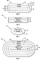
- FIGS 13, 14 and 15 depict various color-shifting foil arrangements.
- the optical article 400 includes a substrate 402 having an upper surface 404 and a lower surface 406.
- the substrate 402 can be flexible or rigid and can be formed of any suitable material such as paper, plastic, cardboard, metal, or the like, and can be opaque or transparent.
- Non-overlapping paired first and second coating structures 408, 410 are disposed on upper surface 404 so as to overlie non-overlapping first and second regions on surface 404.
- first and second coating structures 408, 410 are not superimposed but are physically separated from each other on surface 404, although in an abutting relationship.
- first coating structure 408 can be in the form of a rectangle or square and is disposed within a recess 412 formed by second coating structure 410, also being in the form of a rectangle or square that forms a border or frame that surrounds first coating structure 408.
- second coating structure 410 also being in the form of a rectangle or square that forms a border or frame that surrounds first coating structure 408.
- the first coating structure 408 has a first pigment 414 formed of magnetic pigment flakes or particles, such as color shifting magnetic flakes, constructed in the manner hereinbefore described to provide a magnetic signature.
- the magnetic properties of pigment 414 are provided by a non-optically observable magnetic layer within one or more of the magnetic flakes or particles.
- the second coating structure 410 has a second pigment 416 formed of non-magnetic pigment flakes or particles, such as color shifting non-magnetic flakes.
- the second coating structure 410 could be formed to contain the magnetic pigments and the first coating structure 408 could be formed to contain the non-magnetic pigments.
- the pigments 414, 416 are dispersed in a solidified liquid pigment vehicle 418, 420 of a conventional type so that the pigments 414, 416 produce the desired optical characteristics.
- the liquid vehicle can be a conventional ink vehicle or a conventional paint vehicle of a suitable type.
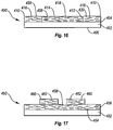
- the optical article 450 includes a substrate 452 having an upper surface region 454.
- the substrate 452 can be formed of the same materials as described for substrate 402 shown in Figure 16 .
- a magnetic pigment coating structure 456 overlies upper surface region 454 of substrate 452.
- the magnetic pigment coating structure 456 includes a plurality of multilayer magnetic pigments 458, such as those described previously, which are dispersed in a solidified pigment vehicle.
- the magnetic properties of the pigment coating structure 456 are provided by a non-optically observable magnetic layer within each of the multilayer magnetic pigments 458.
- a non-magnetic pigment coating structure 460 overlies at least a portion of magnetic pigment coating structure 456.
- the non-magnetic pigment coating structure 460 includes a plurality of non-magnetic pigments 462 dispersed in a solidified pigment vehicle.
- a non-magnetic pigment coating structure can be used in place of magnetic pigment coating structure 456 overlying upper surface region 454 of substrate 452.
- a magnetic pigment coating structure is then used in place of non-magnetic pigment coating structure 460.
- the respective pigment coating in optical articles 400 or 450 can be selected to provide identical colorings or identical color shifting effects to articles 400 and 450, or can be selected to provide different colors or different color shifting effects.
- one skilled in the art will recognize that a variety of combinations of optical features can be used by selecting appropriate coatings or foils with the desired optical characteristics to add various security features to optical articles 400 and 450.
- the pigment coating structures used in articles 400 and 450 may have substantially the same color or color effects, e.g., the same color shifting effects, only one of the pigment coating structures in the articles carries a covert magnetic signature. Therefore, although a human eye cannot detect the magnetic features of the pigment coating structure, a magnetic detection system such as a Faraday rotator detector can be used to detect the magnetic covert signature in the pigment and any information magnetically encoded therein.
- a magnetic detection system such as a Faraday rotator detector can be used to detect the magnetic covert signature in the pigment and any information magnetically encoded therein.
- a structure or device formed with the pigments of the invention can be placed in a bar code pattern which would produce a color shifting bar code device that can appear on a label or on an article itself.
- a bar code would function as a color shifting bar code that could be read by both optical and magnetic readers.
- Such a bar code color shifting device would provide three security features, the bar code itself, the color shifting characteristic, and the magnetic characteristic.
- information can be encoded in the magnetic layers of the pigments of the invention.
- the magnetic layers could record typical information which is carried by a credit card in a magnetic stripe.
- pigments of the invention could be utilized for putting the numbers on the bottoms of checks so that the information carried by the check could be read magnetically as with present day checks while also providing an optical variable feature.
- a three layer magnetic coating sample was prepared with 1000 A Aluminum, 1000 A Iron, and 1000 A Aluminum (Al/Fe/Al).
- the coating sample was prepared in a roll coater, using a 2 mil polyester web coated with an organic release layer (soluble in acetone).
- the particles were filtered and sized by exposing the particles in isopropyl alcohol to ultrasonic agitation for 5 minutes using a Branson sonic welder.
- Particle size was determined using a Horiba LA-300 particle sizing instrument (laser scattering based system). The mean particle size was determined to be 44 pm (22 um standard deviation) in the planar dimension, with a gaussian distribution.
- the pigment particles were filtered and dried.
- a dry weight of magnetic pigment to binder (Du Pont auto refinish paint vehicle) in the ratio of 1: 4 was drawn down onto a thin cardboard sheet (Leneta card).
- a "draw-down" is a paint or ink sample spread on paper to evaluate the color.
- a draw-down is formed with the edge of a putty knife or spatula by "drawing down” a small glob of paint or ink to get a thin film of the paint or ink.
- the draw-down is made using a Mayer rod pulled across a Leneta card and through a small glob of paint.
- a conventional sheet magnet was placed underneath the card while the drawing down was occurring and left in place until the paint vehicle dried.
- the result of the magnetic fields on this pigment sample was to create parallel bright and dark areas in the pigment.
- the bright aluminum areas of the pigment sample had a reflective luminance, Y, of 53% whereas the dark areas had a reflective luminance of 43%.
- it was difficult to fit aperture within the dark and bright lines suggesting that the difference in brightness may actually be larger than these measurements.
- a magnetic ink sample was prepared by mixing a 0.5 g sample of the magnetic pigment of Example 1 (Al/Fe/Al) with 3.575 g of standard Intaglio ink vehicle (high viscosity ink vehicle) and 0.175 g of an ink dryer.
- the ink sample was drawn down onto paper using a flat putty knife.
- a magnetic strip with the word "FLEX” cut out from it was placed beneath the paper during the drawing down step.
- the pattern of the magnetic lines in the dried magnetic ink was readily visible as black and white (silver color) strips with the word “FLEX” readily apparent.
- the optical image of the word "FLEX” in the ink sample was visible at normal incidence and at approximately a 45 degree angle of viewing.
- a magnetic ink sample was prepared as in Example 2 using an Intaglio ink vehicle and coated over paper having a sheet magnet placed behind it.
- the magnet had a cut out of a stylized letter "F.”
- the cut out "F” was embossed upward away from the paper and was bright silver in appearance.
- the "F” stood out over the surrounding area by about 6 microns. This was caused by the paper pushed slightly into the "F” recess of the magnet by the force of the putty knife drawing down the highly viscous Intaglio ink.
- the "F” area remained bright with the Al/Fe/Al flakes oriented parallel to the surface of the paper but in a stepped-up height above the surrounding coating.
- a stylized letter "F” was cut out of a flexible sheet magnet using an exacto knife.
- a draw-down card was placed on top of and in contact with the sheet magnet.
- a magnetic color shifting pigment according to the invention was mixed with an acrylic resin based vehicle and applied to the card with a #22 wire metering rod.
- the resultant draw-down had striped superimposed black lines that replicated the field pattern outside of the stylized "F” in the sheet magnet below the card.
- the entire surface of the drawn-down card exhibited color shifting effects. Where the pattern of the stylized "F” was observed, the stylized "F” only had color shifting effects, while the background had both color shifting effects and the superimposed black lines.
- the cut out stylized letter " F” pieces from the sheet magnet were used in another draw-down with the same magnetic pigment and vehicle described previously in this example.
- the resultant draw-down had striped superimposed black lines that replicated the field pattern within the cutout stylized "F” magnet pieces.
- the entire surface of the drawn-down exhibited a color shifting effect. Where the pattern of the stylized "F” was observed, the stylized " F " had both color shifting effects and the superimposed black lines, while the background had only color shifting effects.
Abstract
Description
- The present invention relates generally to pigments. In particular, the present invention relates to multilayered pigment flakes which have magnetic layers, and pigment compositions that incorporate multilayer pigment flakes having magnetic layers.
- Various pigments, colorants, and foils have been developed for a wide variety of applications. For example, magnetic pigments have been developed for use in applications such as decorative cookware, creating patterned surfaces, and security devices. Similarly, color shifting pigments have been developed for such uses as cosmetics, inks, coating materials, ornaments, ceramics, automobile paints, anti counterfeiting hot stamps, and anti-counterfeiting inks for security documents and currency.
- Color shifting pigments, colorants, and foils exhibit the property of changing color upon variation of the angle of incident light, or as the viewing angle of the observer is shifted. The color-shifting properties of pigments and foils can be controlled through proper design of the optical thin films or orientation of the molecular species used to form the flake or foil coating structure. Desired effects can be achieved through the variation of parameters such as thickness of the layers forming the flakes and foils and the index of refraction of each layer. The changes in perceived color which occur for different viewing angles or angles of incident light are a result of a combination of selective absorption of the materials comprising the layers and wavelength dependent interference effects. The interference effects, which arise from the superposition of light waves that have undergone multiple reflections, are responsible for the shifts in color perceived with different angles. The reflection maxima changes in position and intensity, as the viewing angle changes, due to changing interference effects arising from light path length differences in the various layers of a material which are selectively enhanced at particular wavelengths.
- Various approaches have been used to achieve such color shifting effects. For example, small multilayer flakes, typically composed of multiple layers of thin films, are dispersed throughout a medium such as paint or ink that may then be subsequently applied to the surface of an object. Such flakes may optionally be overcoated to achieve desired colors and optical effects. Another approach is to encapsulate small metallic or silicatic substrates with varying layers and then disperse the encapsulated substrates throughout a medium such as paint or ink. Additionally, foils composed of multiple layers of thin films on a substrate material have been made.
- One manner of producing a multilayer thin film structure is by forming it on a flexible web material with a release layer thereon. The various layers are deposited on the web by methods well known in the art of forming thin coating structures, such as PVD, sputtering, or the like. The multilayer thin film structure is then removed from the web material as thin film color shifting flakes, which can be added to a polymeric medium such as various pigment vehicles for use as an ink or paint. In addition to the color shifting flakes, additives can be added to the inks or paints to obtain desired color shifting results.
- Color shifting pigments or foils is formed from a multilayer thin film structure that includes the same basic layers. These include an absorber layer(s), a dielectric layer(s), and optionally a reflector layer, in varying layer orders. The coatings can be formed to have a symmetrical multilayer thin film structure, such as:
- absorber/dielectric /reflector/dielectric/absorber; or
- absorber/ dielectric/absorber.
- For example,
U.S. Patent No. 5,135,812 to Phillips et al. discloses color-shifting thin film flakes having several different configurations of layers such as transparent dielectric and semi transparent metallic layered stacks. InU.S. Patent No. 5,278,590 to Phillips et al. a symmetric three layer optical interference coating is disclosed which comprises first and second partially transmitting absorber layers which have essentially the same material and thickness, and a dielectric spacer layer located between the first and second absorber layers. - Color shifting platelets for use in paints are disclosed in
U.S. Patent No. 5,571,624 to Phillips et al . These platelets are formed from a symmetrical multilayer thin film structure in which a first semi opaque layer such as chromium is formed on a substrate, with a first dielectric layer formed on the first semi-opaque layer. An opaque reflecting metal layer such as aluminium is formed on the first dielectric layer, followed by a second dielectric layer of the same material and thickness as the first dielectric layer. A second semi-opaque layer of the same material and thickness as the first semi-opaque layer is formed on the second dielectric layer. - With regard to magnetic pigments,
U.S. Patent No. 4,838,648 to Phillips et al. (hereinafter "Phillips '648") discloses a thin film magnetic color shifting structure wherein the magnetic material can be used as the reflector or absorber layer. One disclosed magnetic material is a cobalt nickel alloy. Phillips '648 discloses flakes and foils with the following structures: - dyed superstrate/absorber/dielectric/magnetic layer/substrate;
- dyed superstrate/absorber/dielectric/magnetic layer/dielectric/absorber/dyed superstrate;
- and
- adhesive/magnetic layer/dielectric/absorber/releasable hardcoat/substrate.
- Patterned surfaces have been provided by exposing magnetic flakes to a magnetic force to effect a physical alteration in the structure of the pigment. For example,
U.S. Patent No. 6,103,361 to Batzar et al. (hereinafter "Batzar") uses pigments made of magnetizable materials to decorate cookware. In particular, Batzar is directed toward controlling the orientation of stainless steel flakes in a fluoropolymer release coating to make patterns where at least some of the flakes are longer than the coating thickness. The patterned substrate is formed by applying magnetic force through the edges of a magnetizable die positioned under a coated base to alter the orientation of the flakes within the coating, thereby inducing an imaging effect or pattern. However, Batzar does not discuss the use of optical thin film stacks or platelets employing a magnetic layer. In addition, although the stainless steel flakes used in Batzar are suitable for decorating cookware, they are poorly reflecting. -
U.S. Patent No. 2,570,856 to Pratt et al (hereinafter "Pratt') is directed to metallic flake pigments which are based on ferromagnetic metal platelets. Like Batzar, however, Pratt uses poorly reflecting metals and does not teach the use of thin film optical stacks. -
U.S. Patent Nos. 5,364,689 and5,630,877 to Kashiwagi et al. , (hereinafter collectively 'the Kashiwagi patents"), disclose methods and apparatus for creating magnetically formed painted patterns. The Kashiwagi patents teach use of a magnetic paint layer, which includes non-spherical magnetic particles in a paint medium. A magnetic field with magnetic field lines in the shape of the desired pattern is applied to the paint layer. The final pattern is created by the different magnetic particle orientations in the hardened paint. - One attempt at incorporating a magnetic layer into a multilayer flake is disclosed in European Patent Publication
EP 686675B1 to Schmid et al.
oxide/absorber/dielectric/magnet/Al/magnet/dielectric/absorber/ oxide Thus, Schmid uses aluminum platelets and then coats these platelets with magnetic materials. However, the overlying magnetic material downgrades the reflective properties of the pigment because aluminum is the second brightest metal (after silver), meaning any magnetic material is less reflective. Further, Schmid starts with aluminum platelets generated from ballmilling, a method which is limited in terms of the layer smoothness that can be achieved. - Patent Publication
EP 710508A1 to Richter et al. -
U.S. Patent No. 3,791,864 to Steingroever (hereinafter "Steingroever") describes a method for patterning magnetic particles by orienting them with a magnetic pattern generated in an underlying prime coating that has previously been patterned by a magnetic field. The prime coat contains magnetic particles of the type MO x 6Fe203 where M can be one or more of the elements Ba, Sr, Co, or Pb. After coating a continuous sheet of liquid coating of the primer, it is hardened and then areas of the primer are magnetized by a magnetic field. Next, a pigment vehicle with magnetic particles suspended therein is then applied. The magnetic particles suspended therein are finally oriented by the magnetic force from the magnetic pattern in the primer, creating the final pattern. However, Steingroever suffers from a diffuse magnetic image in the prime coat, which in tum passes a diffuse image to the topcoat. This reduction in resolution is because high magnetic fields are limited in the resolution they can create. This limitation is due to high magnetic field lines surrounding the intended magnetic image, thereby affecting untargeted magnetic particles in the prime coat and blurring the image. -
WO00/034395A WO02/40599A - Accordingly, there is a need for improved multilayer pigment flakes and foils with magnetic properties that overcome or avoid the above problems and limitations.
- In accordance with the invention as embodied and broadly described herein, pigment flakes are provided which have magnetic properties as defined herein. The pigment flakes can be interspersed into liquid media such as paints or inks to produce colorant compositions for subsequent application to objects or papers.
- These and other features of the present invention will become more fully apparent from the following description and appended claims, or may be learned by the practice of the invention as set forth hereinafter.
- In order to illustrate the manner in which the above-recited and other advantages and features of the invention are obtained, a more particular description of the invention briefly described above will be rendered by reference to specific embodiments thereof which are illustrated in the appended drawings. Understanding that these drawings depict only typical embodiments of the invention and are not therefore to be considered limiting of its scope, the invention will be described and explained with additional specificity and detail through the use of the accompanying drawings in which:
-
Figure 1 is a schematic representation of the coating structure of a magnetic flake; -
Figure 2 is a schematic representation of the coating structure of a magnetic flake; -
Figure 3 is a schematic representation of the coating structure of a magnetic flake; -
Figure 4 is a schematic representation of the coating structure of a magnetic flake according to an embodiment of the invention; -
Figure 5 is a schematic representation of the coating structure of a magnetic flake according to another embodiment of the invention; -
Figure 6 is a schematic representation of the coating structure of a magnetic flake; -
Figure 7 is a schematic representation of the coating structure of a magnetic flake; -
Figure 8 is a schematic representation of the coating structure of a magnetic flake; -
Figure 9 is a schematic representation of the coating structure of a magnetic flake to assist understanding of an embodiment of the invention; -
Figure 10 is a schematic representation of the coating structure of a magnetic flake; -
Figure 11 is a schematic representation of the coating structure of a magnetic flake according to another embodiment of the invention; -
Figure 12 is a schematic representation of the coating structure of a magnetic flake; -
Figure 13 is a schematic representation of the coating structure of a magnetic foil; -
Figure 14 is a schematic representation of the coating structure of a magnetic foil; -
Figure 15 is a schematic representation of the coating structure of a magnetic foil; -
Figure 16 is a schematic representation of the coating structure of an optical article; and -
Figure 17 is a schematic representation of the coating structure of an optical article. - The present invention relates to multilayer pigment flakes which have magnetic layers, and pigment compositions which incorporate the magnetic flakes. The flakes can be used both to create security features which are not visually perceptible, and to create three dimensional-like images for security devices or to add decorative features to a product. The nonvisual security features are provided by burying the magnetic layer between other layers within a flake so that only the overlying layers are exposed.
- The three dimensional-like effects can be provided by exposing the flake to an external magnetic force, thereby orienting the plane of some of the pigments normal to the surface of the coating. The un-oriented pigments lie with their planar surface parallel to the surface of the coating. The three dimensional-like effect is due to the alignment of the particles such that the aspect ratio is oriented with the magnetic field, i.e. the longest part of the pigment aligns itself along the magnetic field lines. In such case, the face of the pigment is turned away from the observer to various extents depending on the magnitude of the magnetic force. In the limit or maximum orientation, the coating appears black in color. As one moves off the black, one moves slowly toward the color of the planar surface of the pigment, i.e., color shifting, non-color shifting, such as the color blue, or silver as for example, aluminum. The result is a colored three dimensional-like effect, similar to that of a holographic effect, that appears to move as the viewing angle changes. Methods of creating three dimensional-like images using the magnetic pigments disclosed herein are described in further detail in a
U.S. Patent No. 6,759,097 , and entitled Methods For Producing Imaged Coated Articles By Using Magnetic Pigments. - Unlike many prior magnetic flakes, the presently disclosed flakes are not composed only of magnetizable materials, but include both magnetizable and non magnetizable materials. For example, the invention encompasses pigment flakes wherein a magnetic layer is buried within one or more reflector layers.
- The pigment flakes comprise a magnetic core surrounded by dielectric layers.
- In the case of magnetic layers buried between or within overlying reflector layers, the present invention presents a significant improvement over the prior art by substantially achieving higher chroma and brightness. By putting the duller magnetic material inside the reflector, the present invention accomplishes two objectives: 1) the reflectivity of the reflector layer is maintained; and 2) color shifting pigments without the inner core of magnetic material cannot be distinguished by an observer from such pigment with the core of magnetic material. For example, two coated objects viewed side by side, one with and one without the magnetic material in the coating, would look the same to the observer. However, the magnetic color shifting pigment provides a covert security feature in addition to the color shifting effect. Thus, with a magnetic detection system, a magnetic covert signature in the pigment could be read by a Faraday rotator detector, for example.
- The pigment flakes have substantial shifts in chroma and hue with changes in angle of incident light or viewing angle of an observer. Such an optical effect, known as goniochromaticity or "color shift," allows a perceived color to vary with the angle of illumination or observation. Accordingly, such pigment flakes exhibit a first color at a first angle of incident light or viewing and a second color different from the first color at a second angle of incident light or viewing. The pigment flakes can be interspersed into liquid media such as paints or inks to produce various color shifting colorant compositions for subsequent application to objects or papers.
- The color shifting flakes can be formed using conventional thin film deposition techniques, which are well known in the art of forming thin coating structures. Non-limiting examples of such thin film deposition techniques include physical vapor deposition (PVD), chemical vapor deposition (CVD), plasma enhanced (PE) variations thereof such as PECVD or downstream PECVD, sputtering, electrolysis deposition, and other like deposition methods that lead to the formation of discrete and uniform thin film layers.
- The color shifting pigment flakes of the invention can be formed by various fabrication methods. For example, the pigment flakes can be formed by a web coating process in which various layers are sequentially deposited on a web material by conventional deposition techniques to form a thin film structure, which is subsequently fractured and removed from the web, such as by use of a solvent, to form a plurality of thin film flakes.
- In another fabrication method, one or more thin film layers including at least the magnetic layer is deposited on a web to form a film, which is subsequently fractured and removed from the web to form a plurality of pigment preflakes. The preflakes can be :fragmented further by grinding if desired. The preflakes are then coated with the remaining layer or layers in a sequential encapsulation process to form a plurality of pigment flakes.
- Referring now to the drawings, wherein like structures are provided with like reference designations, the drawings only show the structures necessary to understand the present invention.
Figure 1 depicts a reflective magnetic flake ("RMF") 20. TheRMF 20 is a three layer design having a generally symmetrical thin film structure with a central magnetic layer 22 and at least one reflector layer on either or both of the opposing major surfaces of the central magnetic layer. Thus,RMF 20 comprises a magnetic layer inter-disposed between areflector layer 24 and an opposing reflector layer 26. By inserting the magnetic layer between the highly reflective reflector layers, such as aluminium, the optical properties of the reflector layers are not degraded and the flake remains highly reflective. TheRMF 20 can be used as a pigment flake or can be used as a core section with additional layers applied there over such as in a color shifting pigment. In the case of color shifting pigments, maintaining the high reflective layer is extremely important to preserve high brightness and chroma. Each of these layers in the coating structure ofRMF 20 is discussed below in greater detail. - The magnetic layer 22 can be formed of any magnetic material such as nickel, cobalt, iron, gadolinium, terbium, dysprosium, erbium, and their alloys or oxides. For example, a cobalt nickel alloy can be employed, with the cobalt and nickel having a ratio by weight of about 80% and about 20%, respectively. This ratio for each of these metals in the cobalt nickel alloy can be varied by plus or minus about 10% and still achieve the desired results. Thus, cobalt can be present in the alloy in an amount from about 70% to about 90% by weight, and nickel can be present in the alloy in an amount from about 10% to about 30% by weight. Other examples of alloys include Fe/Si, Fe/Ni, FeCo, Fe/Ni/Mo, and combinations thereof. Hard magnetics of the type SmCo5, NdCo5, Sm2Co17, Nd2Fe14B, Sr6Fe2O3, TbFe2, Al-Ni-Co, and combinations thereof, can also be used as well as spinel ferrites of the type Fe3O4, NiFe2O4, MnFe2O4, CoFe2O4, or garnets of the type YIG or GdIG, and combinations thereof. The magnetic material may be selected for its reflecting or absorbing properties as well as its magnetic properties. When utilized to function as a reflector, the magnetic material is deposited to a thickness so that it is substantially opaque. When utilized as an absorber, the magnetic material is deposited to a thickness so that it is not substantially opaque. A typical thickness for the magnetic material when utilized as an absorber is from about 2 nm to about 20 nm.
- Although this broad range of magnetic materials can be used, the "soft" magnets are preferred in some embodiments of the invention. As used herein, the term "soft magnets" refers to any material exhibiting ferromagnetic properties but having a remanence that is substantially zero after exposure to a magnetic force. Soft magnets show a quick response to an applied magnetic field, but have very low (coercive fields (Hc) = 0.05-300 Oersteds (Oe)) or zero magnetic signatures, or retain very low magnetic lines of force after the magnetic field is removed. Similarly, as used herein, the term 'hard magnets" (also called permanent magnets) refers to any material that exhibits ferromagnetic properties and that has a long lasting remanence after exposure to a magnetizing force. A ferromagnetic material is any material that has a permeability substantially greater than 1 and that exhibits magnetic hysteresis properties.
- Preferably, the magnetic materials used to form magnetic layers in the flakes of the invention have a coercivity of less than about 2000 Oe, more preferably less than about 300 Oe. Coercivity refers to the ability of a material to be demagnetized by an external magnetic field. The higher the value of coercivity, the higher the magnetic field required to de-magnetize the material after the field is removed. In some embodiments of the invention, the magnetic layers used are preferably "soft" magnetic materials (easily demagnetized), as opposed to 'hard" magnetic materials (difficult to demagnetize) which have higher coercivities. The coercivities of pigments or colorants of the magnetic color shifting designs according to the invention are preferably in a range of about 50 Oe to about 300 Oe. These coercivities are lower than in standard recording materials. Thus, preferred embodiments of the invention which use soft magnets in magnetic color shifting pigments and magnetic non color shifting pigments are an improvement over conventional technologies. The use of soft magnetic materials in pigment flakes allows for easier dispersion of the flakes without clumping.
- The magnetic layer 22 can be formed to have a suitable physical thickness of from about 200 angstroms (Å) to about 10,000 Å, and preferably from about 500 Å to about 1,500 Å However, it will be appreciated by those skilled in the art, in view of the disclosure herein, that the optimal magnetic thickness will vary depending on the particular magnetic material used and the purpose for its use. For example, a magnetic absorber layer will be thinner than a magnetic reflector layer based on the optical requirements for such layers, while a covert magnetic layer will have a thickness based solely on its magnetic properties.
- The reflector layers 24 and 26 can be composed of various reflective materials. Presently preferred materials are one or more metals, one or more metal alloys, or combinations thereof, because of their high reflectivity and ease of use, although non-metallic reflective materials could also be used. Non-limiting examples of suitable metallic materials for the reflector layers include aluminium, silver, copper, gold, platinum, tin, titanium, palladium, nickel, cobalt, rhodium, niobium, chromium, and combinations or alloys thereof. The reflector layers 24, 26 can be formed to have a suitable physical thickness of from about 400Å to about 2,000 Å, and preferably from about 500Å to about 1,000 Å.
- In an alternative arrangement, opposing dielectric layers may optionally be added to overlie reflector layers 24 and 26. These opposing dielectric layers add durability, rigidity, and corrosion resistance to
RMF 20. Examples of suitable dielectric materials for the dielectric layers are described hereafter. -
Figure 2 depicts a magnetic color shiftingpigment flake 40 based upon a RMF. Theflake 40 is a generally symmetrical multilayer thin film structure having layers on opposing sides of aRMF 42. Thus, first and second dielectric layers 44 and 46 are disposed respectively on opposing sides ofRMF 42, and first and second absorber layers 48 and 50 are disposed respectively on each ofdielectric layers Figure 1 while the dielectric and absorber layers are discussed below in greater detail. - The dielectric layers 44 and 46 act as spacers in the thin film stack structure of
flake 40. These layers are formed to have an effective optical thickness for imparting interference color and desired color shifting properties. The dielectric layers may be optionally clear, or may be selectively absorbing so as to contribute to the color effect of a pigment. The optical thickness is a well known optical parameter defined as the product 11d, where 11 is the refractive index of the layer and d is the physical thickness of the layer. Typically, the optical thickness of a layer is expressed in terms of a quarter wave optical thickness (QWOT) that is equal to 4ήd/λ., where λ. is the wavelength at which a QWOT condition occurs. The optical thickness of dielectric layers can range from about 2 QWOT at a design wavelength of about 400 nm to about 9 QWOT at a design wavelength of about 700 nm, and preferably 2-6 QWOT at 400-700 nm, depending upon the color shift desired. The dielectric layers typically have a physical thickness of about 100 nm to about 800 nm, depending on the color characteristics desired. - Suitable materials for
dielectric layers - Examples of suitable high refractive index materials for the dielectric layer include zinc sulfide (ZnS), zinc oxide (ZnO), zirconium oxide (ZrO2), titanium dioxide (TiO2), diamond-like carbon, indium oxide (In2O3), indium-tin-oxide (ITO), tantalum pentoxide (Ta2O5), eerie oxide (CeO2), yttrium oxide (Y2O3), europium oxide (Eu2O3), iron oxides such as (II)diiron(III) oxide (Fe3O4) and ferric oxide (Fe2O3), hafuium nitride (HfN), hafuium carbide (HfC), hafuium oxide (HfO2), lanthanum oxide (La2O3), magnesium oxide (MgO), neodymium oxide (Nd2O3), praseodymium oxide (Pr6O11), samarium oxide (Sm2O3), antimony trioxide (Sb2O3), silicon monoxide (SiO), selenium trioxide (Se2O3), tin oxide (SnO2), tungsten trioxide (WO3), combinations thereof, and the like.
- Suitable low refractive index materials for the dielectric layer include silicon dioxide (SiO2), aluminum oxide (Al2O3), metal fluorides such as magnesium fluoride (MgF2), aluminum fluoride (AlF3), cerium fluoride (CeF3), lanthanum fluoride (LaF3), sodium aluminum fluorides (e.g., Na3AIF6 or Na5Al3F14), neodymium fluoride (NdF3), samarium fluoride (SmF3), barium fluoride (BaF2), calcium fluoride (CaF2), lithium fluoride (LiF), combinations thereof, or any other low index material having an index of refraction of about 1.65 or less. For example, organic monomers and polymers can be utilized as low index materials, including dienes or alkenes such as acrylates (e.g., methacrylate), perfluoroalkenes, polytetrafluoroethylene (Teflon), fluorinated ethylene propylene (FEP), combinations thereof, and the like.
- It should be appreciated that several of the above-listed dielectric materials are typically present in non-stoichiometric forms, often depending upon the specific method used to deposit the dielectric material as a coating layer, and that the above listed compound names indicate the approximate stoichiometry. For example, silicon monoxide and silicon dioxide have nominal 1:1 and 1:2 silicon:oxygen ratios, respectively, but the actual silicon:oxygen ratio of a particular dielectric coating layer varies somewhat from these nominal values. Such non-stoichiometric dielectric materials are also within the scope of the present invention.
- As mentioned above, the dielectric layers can be formed of high/low dielectric optical stacks, which have alternating layers of low index (L) and high index (H) materials. When a dielectric layer is formed of a high/low dielectric stack, the color shift at angle will depend on the combined refractive index of the layers in the stack. Examples of suitable stack configurations for the dielectric layers include LH, HL, LHL, HLH, HLHL, LHLH, or in general L(HL)n or H(LH)n, where n = 1-100, as well as various multiples and combinations thereof. In these stacks, LH, for example, indicates discrete layers of a low index material and a high index material. In an alternative embodiment, the high/low dielectric stacks are formed with a gradient index of refraction. For example, the stack can be formed with layers having a graded index low-to-high, a graded index high-to-low, a graded index [low-to-high-to-low]n, a graded index [high-to-low-to-high]n, where n = 1-100, as well as combinations and multiples thereof The graded index is produced by a gradual variance in the refractive index, such as low-to-high index or high-to-low index, of adjacent layers. The graded index of the layers can be produced by changing gases during deposition or co-depositing two materials (e.g., L and H) in differing proportions. Various high/low optical stacks can be used to enhance color shifting performance, provide antireflective properties to the dielectric layer, and change the possible color space of the pigments of the invention.
- The dielectric layers can each be composed of a different material, and/or can have different optical or physical thickness for each layer. It will be appreciated that when the dielectric layers are composed of different materials or have different thicknesses, the flakes exhibit different colors on each side thereof and the resulting mix of flakes in a pigment or paint mixture would show a new color which is the combination of the two colors. The resulting color would be based on additive color theory of the two colors coming from the two sides of the flakes. In a multiplicity of flakes, the resulting color would be the additive sum of the two colors resulting from the random distribution of flakes having different sides oriented toward the observer.
- The absorber layers 48, 50 of
flake 40 can be composed of any absorber material having the desired absorption properties, including materials that are uniformly absorbing or non-uniformly absorbing in the visible part of the electromagnetic. spectrum. Thus, selective absorbing materials or nonselective absorbing materials can be used, depending on the color characteristics desired. For example, the absorber layers can be formed of nonselective absorbing metallic materials deposited to a thickness at which the absorber layer is at least partially absorbing, or semi-opaque. Non-limiting examples of suitable absorber materials include metallic absorbers such as chromium, aluminium, nickel, silver, copper, palladium, platinum, titanium, vanadium, cobalt, iron, tin, tungsten, molybdenum, rhodium, and niobium, as well as their corresponding oxides, sulphides, and carbides. Other suitable absorber materials include carbon, graphite, silicon, germanium, cermet, ferric oxide or other metal oxides, metals mixed in a dielectric matrix, and other substances that are capable of acting as a uniform or selective absorber in the visible spectrum. Various combinations, mixtures, compounds, or alloys of the above absorber materials may be used to form the absorber layers offlake 40. - Examples of suitable alloys of the above absorber materials include Inconel (Ni-Cr-Fe), stainless steels, Hastalloys (e.g., Ni-Mo-Fe; Ni-Mo-Fe-Cr; Ni-Si-Cu) and titanium-based alloys, such as titanium mixed with carbon (Ti/C), titanium mixed with tungsten (Ti/W), titanium mixed with niobium (Ti/Nb), and titanium mixed with silicon (Ti/Si), and combinations thereof. As mentioned above, the absorber layers can also be composed, of an absorbing metal oxide, metal sulphide, metal carbide, or combinations thereof. For example, one preferred absorbing sulphide material is silver sulphide.
- Other examples of suitable compounds for the absorber layers include titanium-based compounds such as titanium nitride (TiN), titanium oxynitride (TiNxOy), titanium carbide (TiC), titanium nitride carbide (TiNxCz), titanium oxynitride carbide (TiNxOyCz), titanium silicide (TiSi2), titanium boride (TiB2), and combinations thereof. In the case of TiNxOy and TiNxOyCz, preferably x = 0 to 1, y = 0 to 1, and z = 0 to 1, where x + y = 1 in TiNxOy and x + y + z = 1 in TiNxOyCz. For TiNxCz, preferably x = 0 to 1 and z = 0 to 1, where x + z = 1. Alternatively, the absorber layers can be composed of a titanium-based alloy disposed in a matrix of Ti, or can be composed of Ti disposed in a matrix of a titanium-based alloy.
- It will be appreciated by one skilled in the art that the absorber layer also could be formed of a magnetic material, such as a cobalt nickel alloy. This simplifies the manufacture of the magnetic color shifting device or structure by reducing the number of materials required.
- The absorber layers are formed to have a physical thickness in the range from about 30 Å to about 500 Å, and preferably about 50 Å to about 150 Å, depending upon the optical constants of the absorber layer material and the desired peak shift. The absorber layers can each be composed of the same material or a different material, and can have the same or different physical thickness for each layer.
-
Figure 3 depicts a reflective magnetic flake or particle ("RMP") 60. TheRMP 60 is a two layer design with areflector layer 62 substantially surrounding and encapsulating a coremagnetic layer 64. -
Figure 4 depicts alternative coating structures (with phantom lines) for a magnetic color shiftingpigment flake 80 in the form of an encapsulate based upon either the RMF or the RMP according to an embodiment of the invention. Theflake 80 has amagnetic core section 82, which is either a RMF or a RMP, which can be overcoated by an encapsulatingdielectric layer 84 substantially surroundingmagnetic core section 82. Anabsorber layer 86, which overcoatsdielectric layer 84, provides a n outer encapsulation offlake 80. The hemispherical dashed lines on one side offlake 80 inFigure 4 indicate thatdielectric layer 84 andabsorber layer 86 can be formed as contiguous layers aroundmagnetic core section 82. - Alternatively, the
magnetic core section 82 and dielectric layer can be in the form of a thin film core flake stack, in which opposingdielectric layers 84A and 84b are preformed on the top and bottom surfaces but not on at least one side surface of magnetic core section 82 (RMF), withabsorber layer 86 encapsulating the thin film stack. An encapsulation process can Also be used to form additional layers onflake 80 such as a capping layer (not shown). Thepigment flake 80 exhibits a discrete color shift such that the pigment flake has a first color At a first angle of incident light or viewing and a second color different from the first color at a second angle of incident light or viewing. -
Figure 5 depicts another alternative coating structure for a color shiftingpigment flake 100 according to an embodiment of the invention. Theflake 100 includes amagnetic core section 82 and asingle dielectric layer 84, which extends over top and bottom surfaces ofmagnetic core section 82 to form a dielectric-coatedpreflake 86. Thecore section 82 can be an RMF, RMP, or a magnetic layer. The dielectric-coatedpreflake 86 has twoside surfaces 88 and 90. Althoughside surface 90 is homogeneous and formed only of the dielectric material ofdielectric layer 84, side surface 88 hasdistinct surface regions 88A, 88b, 88c of dielectric, magnetic core section, and dielectric, respectively. The dielectric-coatedpreflake 86 is further coated on all sides with anabsorber layer 92. Theabsorber layer 92 is in contact withdielectric layer 84 andmagnetic core section 82 at side surface 88. - The structure of
pigment flake 100 typically occurs because of a preflake coating process. The preflakes can be a dielectric-coated flake, in which a dielectric coating completely encapsulates an RMF or RMP (seeFigure 4 ), or a magnetic layer (seeFigure 10 ). The preflakes a re broken into sized preflakes using any conventional fragmentation process, such as by grinding. The sized preflakes will include some sized preflakes having top and bottom dielectric layers with no dielectric coating on the side surfaces of the preflake, such as shown for the embodiment offlake 40 inFigure 2 in whichRMF 42 is coated with top and bottom dielectric layers 44 and 46. Other sized preflakes will have a single dielectric layer extending over both top a nd bottom surfaces of the magnetic core flake section, leaving one side surface of the magnetic core flake section exposed, such As shown for dielectric-coatedpreflake 86 inFigure 5 . Because of the :fragmentation process, substantially a II of the sized preflakes have at least a portion of a side surface exposed. The sized preflakes are then coated on all sides with an absorber layer, such as shown in the flakes ofFigures 4 and5 . -
Figure 6 depicts a composite magnetic flake ("CMF") 120 which comprises a centraldielectric support layer 122 with first and secondmagnetic layers CMF 120 is significantly stabilized And strengthened, having increased rigidity. Additional dielectric layers (not shown) may optionally be added to overliemagnetic layers CMF 120. TheCMF 120 can be used as a magnetic core section with additional layers applied there over. Themagnetic layers - The dielectric material used for
support layer 122 is preferably inorganic, since inorganic dielectric materials have been found to have good characteristics of brittleness and rigidity. Various dielectric materials that can be utilized include metal fluorides, metal oxides, metal sulphides, metal nitrides, metal carbides, combinations thereof, and the like. The dielectric materials may be in either a crystalline, amorphous, or semi-crystalline state. These materials are readily available and easily applied by physical or chemical vapour deposition processes. Examples of suitable dielectric materials include magnesium fluoride, silicon monoxide, silicon dioxide, aluminium oxide, titanium dioxide, tungsten oxide, aluminium nitride, boron nitride, boron carbide, tungsten carbide, titanium carbide, titanium nitride, silicon nitride, zinc sulphide, glass flakes, diamond-like carbon, combinations thereof, and the like. Alternatively,support layer 122 may be composed of a preformed dielectric or ceramic preflake material having a high aspect ratio such as a natural platelet mineral (e.g., mica peroskovite or talc), or synthetic platelets formed from glass, alumina, silicon dioxide, carbon, micaceous iron oxide, coated mica, boron nitride, boron carbide, graphite, bismuth oxychloride, various combinations thereof, and the like. - In an alternative arrangement, instead of a
dielectric support layer 122, various semi-conductive conductive materials having a sufficient ratio of tensile to compressive strength can function a s a support layer. Examples of such materials include silicon, metal silicides, semi-conductive compounds formed from any of the group III, IV, or V elements, metals having a body centered cubic crystal structure, cermet compositions or compounds, semi-conductive glasses, various combinations thereof, and the like. It will be appreciated from the teachings herein, however, that Any support material providing the functionality described herein and capable of acting as a rigid layer with glass-like qualities would be an acceptable substitute for one of these materials. - The thickness of
support layer 122 can be in a range from about 10 nm to about 1,000 nm, preferably from about 50 nm to about 200 nm, although these ranges should not be taken as restrictive. -
Figure 7 depicts a composite magnetic particle ("CMP") 140. TheCMP 140 is a two layer design with amagnetic layer 142 substantially surrounding and encapsulating acentral support layer 144 such as a dielectric layer. -
Figure 8 depicts a coating structure for a color shiftingpigment flake 160 in the form of an encapsulate. - Various coating processes can be utilized i n forming the dielectric and absorber coating layers by encapsulation. For example, suitable preferred methods for forming the dielectric layer include vacuum vapour deposition, sol-gel hydrolysis, CVD in a fluidized bed, downstream plasma onto vibrating trays filled with particles, and electrochemical deposition. A suitable Si02 sol-gel process is described in
U.S. Patent No. 5,858,078 to Andes et al. Other examples of suitable sol-gel coating techniques useful in the present invention are disclosed inU.S. Patent No. 4,756,771 to BrodaIIA ; Zink et Al., Optical Probes And Properties of aluminosilicate Glasses Prepared by the Sol-Gel Method, Polym. Mater. Sci. Eng., 61, pp. 204-208 (1989); And McKiemAn et Al., Luminescence And Laser Action of Coumarin Dyes Doped in Silicate And Aluminosilicate Glasses Prepared by the Sol-Gel Technique, J. Inorg. Organomet. Polym., 1(1), pp. 87-103 (1991). - Suitable preferred methods for forming the absorber layers include vacuum vapour deposition, and sputtering onto a mechanically vibrating bed of particles, as disclosed
US Patent 6,241,858 filed September 3, 1999 , entitled "Methods and Apparatus for Producing Enhanced Interference Pigments". Alternatively, the absorber coating may be deposited by decomposition through pyrolysis of metal-organo compounds or related CVD processes which may be carried out in a fluidized bed as described inU.S. Patent Nos. 5,364,467 and5,763,086 to Schmid et al. If no further grinding is carried out, these methods result in an encapsulated core flake section with dielectric and absorber materials therearound. Various combinations of the above coating processes may be utilized during manufacture of pigment flakes with multiple encapsulating coatings. - In one method of forming the absorber coating, powdered flakes or other coated preflakes are placed on a square-shaped vibrating conveyor coater in a vacuum coating chamber as disclosed in
U.S. Patent No. 6,241,858 , discussed above. The vibrating conveyor coater includes conveyor trays which are configured in an overlapping inclined arrangement so that the powdered flakes travel along a circulating path within the vacuum chamber. While the flakes circulate along this path they are effectively mixed by constant agitation so that exposure to the vaporized absorber coating material is uniform. Efficient mixing also occurs at the end of each conveyor tray as the flakes drop in a waterfall off of one tray and onto the next tray. The Absorber can be sequentially coated on the flakes as they repeatably move under a coating material source. - When using vibrating conveyer trays to coat the absorber, it is important that the powdered flakes tumble randomly under the coating material source such as sputter targets and do not become subject to "metal welding" or sticking. Such metal welding or sticking can occur between two flat surfaces of reactive metals when such metals are deposited in a vacuum. For example, aluminum has a high propensity to stick to itself, whereas chromium does not. Suitable absorber materials can be applied as either a single material or as an outer capping layer over an underlying different absorber material.
-
Figure 9 depicts a dielectric coated magnetic flake ("DMF") 180 according to aid understanding of the invention. TheDMF 180 is a three-layer design having a generally symmetrical thin film structure with a central magnetic layer and at least one dielectric layer on either or both of the opposing major surfaces of the central magnetic layer. Thus, as shown,DMF 180 includes amagnetic layer 182 sandwiched in between adielectric layer 184 and an opposingdielectric layer 186. By inserting the magnetic layer between the dielectric layers, the DMF has increased rigidity and durability. -
Figure 10 depicts a dielectric coated magnetic particle ("DMP") 200. TheDMP 200 is a two layer design with adielectric layer 202 substantially surrounding and encapsulating a centralmagnetic layer 204. - Each of the layers in the coating structures of
DMF 180 andDMP 200 can be formed of the same materials and thickness as corresponding layers described in previous embodiments. For example, the dielectric layer inDMF 180 andDMP 200 can be formed of the same materials and in the same thickness ranges as taught herein above fordielectric layer 44 offlake 40, and the magnetic layers inDMF 180 andDMP 200 can be formed of the same materials and in the same thickness ranges as taught herein above for magnetic layer 22 offlake 20. TheDMF 180 andDMP 200 can each be used as a pigment flake or particle, or can be used as a magnetic core section with additional layers applied thereover. -
Figure 11 depicts a color shiftingpigment flake 220 according to another embodiment of the invention which does not use a reflector (with high reflectance, i.e., an optical metal). Theflake 220 is a three-layer design having a generally symmetrical multilayer thin film structure on opposing sides of amagnetic core section 222, which can be a DMF or a DMP. Thus, first andsecond absorber layers flake 220 can be formed by a web coating and flake removal process as described previously. -
Figure 11 further depicts an alternative coating structure (with phantom lines) forcolor shifting flake 220, in which the absorber layer is coated aroundmagnetic core section 222 in an encapsulation process. accordingly,absorber layers continuous coating layer 224 substantially surrounding the flake structure thereunder. - Thus,
pigment flake 220 may be embodied either as a multilayer thin film stack flake or a multilayer thin film encapsulated particle. Suitable materials and thicknesses for the absorber, dielectric, and magnetic layers offlake 220 are the same as taught hereinabove. - Some flakes of the invention can be characterized as multilayer thin film interference structures in which layers lie in parallel planes such that the flakes have first and second parallel planar outer surfaces and an edge thickness perpendicular to the first and second parallel planar outer surfaces. Such flakes are produced to have an aspect ratio of at least about 2:1, and preferably about 5-15:1 with a narrow particle size distribution. The aspect ratio of the flakes is ascertained by taking the ratio of the longest planar dimension of the first and second outer surfaces to the edge thickness dimension of the flakes.
- One presently preferred method of fabricating a plurality of pigment flakes, each of which having the multilayer thin film coating structure of
flake 40 shown inFigure 2 , is based on conventional web coating techniques used to make optical thin films. Althoughflake 40 is described herein below, the other flake structures taught herein can also be fabricated with a procedure similar to the one described herein below. Accordingly, a first absorber layer is deposited on a web of flexible material such as polyethylene terephthalate (PET) which has an optional release layer thereon. The absorber layer can be formed by a conventional deposition process such as PVD, CVD, PECVD, sputtering, or the like. The above mentioned deposition methods enable the formation of a discrete and uniform absorber layer of a desired thickness. - Next, a first dielectric layer is deposited on the absorber layer to a desired optical thickness by a conventional deposition process. The deposition of the dielectric layer can be accomplished by a vapour deposition process (e.g., PVD, CVD, PECVD), which results in the dielectric layer cracking under the stresses imposed as the dielectric transitions from the vapour into the solid phase.
- The magnetic core is then deposited. In the case of reflector layers, a first reflector layer is then deposited by PVD, CVD, or PECVD on the first dielectric layer, taking on the characteristics of the underlying cracked dielectric layer. Magnetic layers are then applied by e-beam evaporation, sputtering, electrodeposition, or CVD, followed by a second reflector layer being deposited.
- This is followed by a second dielectric layer being deposited on the second reflector layer and preferably having the same optical thickness as the first dielectric layer. Finally, a second Absorber layer is deposited on the second dielectric layer and preferably has the same physical thickness as the first absorber layer.
- Thereafter, the flexible web is removed, either by dissolution in a preselected liquid or by way of a release layer, both of which Are well known to those skilled in the art. As a result, a plurality of flakes are fractured out along the cracks of the layers during removal of the web from the multilayer thin film. This method of manufacturing pigment flakes is similar to that more fully described in
U.S. Patent No. 5,135,812 to Phillips et al. , the pigment flakes can be further fragmented if desired by, for example, grinding the flakes to a desired size using an air grind, such that each of the pigment flakes has a dimension on any surface thereof ranging from about 2 microns to about 200 microns. - In order to impart additional durability to the color shifting flakes, an annealing process can be employed to heat treat the flakes at a temperature ranging from about 200-300°C, and preferably from about 250-275°C, for a time period ranging from about 10 minutes to about 24 hours, and preferably a time period of about 15-60 minutes.
- Pigment flake structures, methods of forming them, and additional features compatible therewith can be found in Phillips '648,
U.S. Patent No. 4,705,356 to Berning et al. , andU.S. Patent No. 6,157,489 to Bradley et al. ;U.S. Patents. 6,569,529 to Phillips et al ,6,572,784 to Coombs et al. ,6,656,770 to Mayer et al. ,6241,858 to Phillips et al. , and6,524,381 to Phillips et al . One skilled in the art will recognize, in light of the disclosure herein, that the magnetic layers discussed previously can be combined with the coating structures disclosed in the above patents and applications, such as by replacing a reflector layer with the RMF or RMP disclosed herein to obtain additional useful coating structures. - Referring now to
Figure 12 ,pigment flake 240 is deposited according to another embodiment of the invention. As illustrated,flake 240 is a multilayer design having a generally symmetrical thin film structure on opposing sides of a magnetic layer such as a reflectivemagnetic core 242, which can be any non-color shifting magnetic pigment flake or particle having reflective properties described herein or known in the art. For example, reflectivemagnetic core 242 can be a single reflective magnetic layer such as a monolithic layer of Ni or other magnetic reflective metal, or can be a multilayer magnetic structure such as AI/Fe/AI. A first colored layer such asselective absorber layer 244a and a second colored layer such asselective absorber layer 244b are formed on opposing major surfaces of reflectivemagnetic core 242. These colored layers offlake 240 can be formed by a web coating and flake removal process as described previously. -
Figure 12 further depicts an alternative coating structure (with phantom lines) forflake 240, in which a colored layer such asselective absorber layer 244 is coated around reflectivemagnetic core 242 in an encapsulation process. Accordingly,selective absorber layers contiguous coating layer 244 substantially surrounding the flake structure thereunder. Suitable encapsulation methods for formingflake 240 are as described inU.S. Patent No. 6,586,098, filed July 27, 2000 . - Thus,
pigment flake 240 may be embodied either as a multilayer thin film stack flake or a multilayer thin film encapsulated particle. Suitable materials and thicknesses for use in the reflective magnetic core offlake 240 are the same as taught hereinabove, so long as both reflective and magnetic properties are maintained. - The colored layers of
flake 240 can be formed of a variety of different absorbing and/or reflecting materials in one or more layers. Preferably, the colored layers such as selective absorber layers are formed to have a thickness of from about 0.05 µm to about 5 µm, and more preferably from about 1 µm to about 2 µm, by conventional coating processes for dye stuffs, when an organic dye material is utilized to form the selective absorber layers. Preferably, the colored layers are formed to have a thickness of from about 0.05 µm to about 0.10 µm when colored metallic or other inorganic colorant materials are utilized. - Examples of suitable organic dyes that can be used to form the selective absorber layers of
flake 240 include copper phthalocyanine, perylene-based dyes, anthraquinone-based dyes, and the like; azo dyes and azo metal dyes such as aluminum red (RLW), aluminum copper, aluminum bordeaux (RL), aluminum fire- red (ML), aluminum red (GLW), aluminum violet (CLW), and the like; as well as combinations or mixtures thereof. Such dyes can be applied by conventional coating techniques and even by evaporation. - The colored layers of
flake 240 can also be formed of a variety of conventional organic or inorganic pigments applied singly or dispersed in a pigment vehicle. Such pigments are described in the NPIRI raw Materials Data Handbook, Vol. 4, Pigments (1983). - In another embodiment, the selective absorber layers of
flake 240 comprise a sol-gel matrix holding a colored pigment or dye. For example, the selective absorber layer can be formed of aluminum oxide or silicon dioxide applied by a sol-gel process, with organic dyes absorbed into pores of the sol-gel coating or bound to the surface of the coating. suitable organic dyes used in the sol-gel coating process include those available under the trade designations Aluminumrot GLW (aluminum red GLW) and Aluminumviolett CLW (aluminum violet CLW) from the Sandoz Company. Aluminum red GLW is an azo metal complex containing copper, and aluminum violet CLW is a purely organic azo dye. Examples of sol-gel coating techniques useful in the present invention are disclosed in the following:U.S. Patent No. 4,756,771 to Brodalla (1988 ); Zink et al., Optical Probes and Properties of Aluminosilicate Glasses Prepared by the Sol-Gel Method, Polym. Mater. Sci. Eng., 61, pp. 204-208 (1989); And McK.ieman et al., Luminescence and Laser Action of Coumarin Dyes Doped in Silicate and Aluminosilicate Glasses Prepared by the Sol-Gel Technique, J. Inorg. Organomet. Polym., 1(1), pp. 87-103 (1991). - In a further embodiment, the colored layers of
flake 240 can be formed of an inorganic colorant material. Suitable inorganic colorants include selective absorbers such as titanium nitride, chromium nitride, chromium oxide, iron oxide, cobalt-doped alumina, and the like, as well as colored metallic such as copper, brass, titanium, and the like. - It should be understood that various combinations of the above dyes, pigments, and colorants may also be employed to achieve a desired color characteristic for
flake 240. The organic dyes, pigments, and colorants discussed herein can be used in the invention to Achieve pigments with bright colors having magnetic properties. - Various modifications and combinations of the foregoing embodiments are also considered within the scope of the invention. For example, additional dielectric, absorber, and/or other optical coatings can be formed around each of the above flake or particle embodiments, or on a composite reflective film prior to flake formation, to yield further desired optical characteristics. Such additional coatings can provide additional color effects to the pigments. For example, a colored dielectric coating added to a color shifting flake would act as a color filter on the flake, providing a subtractive color effect which changes the color produced by the flake.
- The pigment flakes of the present invention can be interspersed within a pigment medium to produce a colorant composition which can be applied to a wide variety of objects or papers. The pigment flakes added to a medium produces a predetermined optical response through radiation incident on a surface of the solidified medium. Preferably, the pigment medium contains a resin or mixture of resins which can be dried or hardened by thermal processes such as thermal cross linking, thermal setting, or thermal solvent evaporation or by photochemical crosslinking. Useful pigment media include various polymeric compositions or organic binders such as alkyd resins, polyester resins, acrylic resins, polyurethane resins, vinyl resins, epoxies, styrenes, and the like. Suitable examples of these resins include melamine, acrylates such as methyl methacrylate, ABS resins, ink and paint formulations based on alkyd resins, and various mixtures thereof. The flakes combined with the pigment media produce a colorant composition that can be used directly as a paint, ink, or moldable plastic material. The colorant composition can also be utilized as an additive to conventional paint, ink, or plastic materials.
- The pigment medium Also preferably contains a solvent for the resin. For the solvent, generally, either an organic solvent or water can be used. A volatile solvent can also be used in the medium. As for the volatile solvent, it is preferable to use a solvent which is both volatile as well as dilatable, such as a thinner. In particular, faster drying of the pigment medium can be achieved by increasing the Amount of the solvent with A low boiling point composition such as methyl ethyl ketone (MEK).
- In addition, the flakes can be optionally blended with various additive materials such as conventional pigment flakes, particles, or dyes of different hues, Chroma and brightness to achieve the color characteristics desired. For example, the flakes can be mixed with other conventional pigments, either of the interference type or non-interference type, to produce a range of other colors. This preblended composition can then be dispersed into a polymeric medium such as a paint, ink, plastic or other polymeric pigment vehicle for use in a conventional manner.
- Examples of suitable additive materials that can be combined with the flakes of the invention include non-color shifting high chroma or high reflective platelets which produce unique color effects, such as MgF2/Al/MgF2 platelets, or SiO2/Al/ SiO2 platelets. Other suitable additives that can be mixed with the magnetic color shifting flakes include lamellar pigments such as multi-layer color shifting flakes, aluminum flakes, graphite flakes, glass flakes, iron oxide, boron nitride, mica flakes, interference based TiO2 coated mica flakes, interference pigments based on multiple coated plate- like silicate substrates, metal-dielectric or all-dielectric interference pigments, and the like; and non-lamellar pigments such as aluminum powder, carbon black, ultramarine blue, cobalt based pigments, organic pigments or dyes, rutile or spinel based inorganic pigments, naturally occurring pigments, inorganic pigments such as titanium dioxide, talc, china clay, and the like; as well as various mixtures thereof For example, pigments such as aluminum powder or carbon black can be added to control lightness and other color properties.
- The magnetic color shifting flakes of the present invention are particularly suited for use in applications where colorants of high chroma and durability are desired. By using the magnetic color shifting flakes in a colorant composition, high chroma durable paint or ink can be produced in which variable color effects are noticeable to the human eye. The color shifting flakes of the invention have a wide range of color shifting properties, including large shifts in chroma (degree of color purity) and also large shifts in hue (relative color) with a varying angle of view. Thus, an object colored with a paint containing the color shifting flakes of the invention will change color depending upon variations in the viewing angle or the angle of the object relative to the viewing eye.
- The pigment flakes of the invention can be easily and economically utilized in paints and inks which can be applied to various objects or papers, such as motorized vehicles, currency and security documents, household appliances, architectural structures, flooring, fabrics, sporting goods, electronic packaging/housing, product packaging, etc. The color shifting flakes can also be utilized in forming colored plastic materials, coating compositions, extrusions, electrostatic coatings, glass, and ceramic materials.
-
Figures 13, 14 and 15 depict various color-shifting foil arrangements. - Referring now to
Figure 16 , anoptical article 400 having paired optical structures. Theoptical article 400 includes asubstrate 402 having anupper surface 404 and alower surface 406. Thesubstrate 402 can be flexible or rigid and can be formed of any suitable material such as paper, plastic, cardboard, metal, or the like, and can be opaque or transparent. Non-overlapping paired first andsecond coating structures upper surface 404 so as to overlie non-overlapping first and second regions onsurface 404. Thus, first andsecond coating structures surface 404, although in an abutting relationship. For example, in one embodiment,first coating structure 408 can be in the form of a rectangle or square and is disposed within a recess 412 formed bysecond coating structure 410, also being in the form of a rectangle or square that forms a border or frame that surroundsfirst coating structure 408. Thus, whenoptical article 400 is viewed from above, coatingstructures - The
first coating structure 408 has afirst pigment 414 formed of magnetic pigment flakes or particles, such as color shifting magnetic flakes, constructed in the manner hereinbefore described to provide a magnetic signature. The magnetic properties ofpigment 414 are provided by a non-optically observable magnetic layer within one or more of the magnetic flakes or particles. Thesecond coating structure 410 has asecond pigment 416 formed of non-magnetic pigment flakes or particles, such as color shifting non-magnetic flakes. Alternatively, thesecond coating structure 410 could be formed to contain the magnetic pigments and thefirst coating structure 408 could be formed to contain the non-magnetic pigments. Thepigments liquid pigment vehicle pigments - Referring now to
Figure 17 , anoptical article 450 having overlapping paired optical structures. Theoptical article 450 includes asubstrate 452 having anupper surface region 454. Thesubstrate 452 can be formed of the same materials as described forsubstrate 402 shown inFigure 16 . A magneticpigment coating structure 456 overliesupper surface region 454 ofsubstrate 452. The magneticpigment coating structure 456 includes a plurality of multilayermagnetic pigments 458, such as those described previously, which are dispersed in a solidified pigment vehicle. The magnetic properties of thepigment coating structure 456 are provided by a non-optically observable magnetic layer within each of the multilayermagnetic pigments 458. A non-magneticpigment coating structure 460 overlies at least a portion of magneticpigment coating structure 456. The non-magneticpigment coating structure 460 includes a plurality ofnon-magnetic pigments 462 dispersed in a solidified pigment vehicle. - In an alternative embodiment of
optical article 450, a non-magnetic pigment coating structure can be used in place of magneticpigment coating structure 456 overlyingupper surface region 454 ofsubstrate 452. A magnetic pigment coating structure is then used in place of non-magneticpigment coating structure 460. - The respective pigment coating in
optical articles articles optical articles - Although the pigment coating structures used in
articles - From the foregoing it can be seen that there have been provided thin film structures which have both magnetic, and optionally, color shifting properties, which have many different types of applications, particularly where additional security is desired.
- For example, a structure or device formed with the pigments of the invention can be placed in a bar code pattern which would produce a color shifting bar code device that can appear on a label or on an article itself. Such a bar code would function as a color shifting bar code that could be read by both optical and magnetic readers. Such a bar code color shifting device would provide three security features, the bar code itself, the color shifting characteristic, and the magnetic characteristic. In addition, information can be encoded in the magnetic layers of the pigments of the invention. For example, the magnetic layers could record typical information which is carried by a credit card in a magnetic stripe. In addition, pigments of the invention could be utilized for putting the numbers on the bottoms of checks so that the information carried by the check could be read magnetically as with present day checks while also providing an optical variable feature.
- The following reference examples are given to help understanding of the present invention.
- A three layer magnetic coating sample was prepared with 1000 A Aluminum, 1000 A Iron, and 1000 A Aluminum (Al/Fe/Al). The coating sample was prepared in a roll coater, using a 2 mil polyester web coated with an organic release layer (soluble in acetone). After stripping the three layer coating from the web to form pigment flake particles, the particles were filtered and sized by exposing the particles in isopropyl alcohol to ultrasonic agitation for 5 minutes using a Branson sonic welder. Particle size was determined using a Horiba LA-300 particle sizing instrument (laser scattering based system). The mean particle size was determined to be 44 pm (22 um standard deviation) in the planar dimension, with a gaussian distribution. Following the sizing, the pigment particles were filtered and dried.
- A dry weight of magnetic pigment to binder (Du Pont auto refinish paint vehicle) in the ratio of 1: 4 was drawn down onto a thin cardboard sheet (Leneta card). A "draw-down" is a paint or ink sample spread on paper to evaluate the color. Typically, a draw-down is formed with the edge of a putty knife or spatula by "drawing down" a small glob of paint or ink to get a thin film of the paint or ink. Alternatively, the draw-down is made using a Mayer rod pulled across a Leneta card and through a small glob of paint. A conventional sheet magnet was placed underneath the card while the drawing down was occurring and left in place until the paint vehicle dried. The result of the magnetic fields on this pigment sample was to create parallel bright and dark areas in the pigment. By using an ultra small area viewer (USAV, 2.3 mm) on a SF-600 DataColor spectrophotometer, the bright aluminum areas of the pigment sample had a reflective luminance, Y, of 53% whereas the dark areas had a reflective luminance of 43%. However, it was difficult to fit aperture within the dark and bright lines suggesting that the difference in brightness may actually be larger than these measurements.
- A magnetic ink sample was prepared by mixing a 0.5 g sample of the magnetic pigment of Example 1 (Al/Fe/Al) with 3.575 g of standard Intaglio ink vehicle (high viscosity ink vehicle) and 0.175 g of an ink dryer. The ink sample was drawn down onto paper using a flat putty knife. A magnetic strip with the word "FLEX" cut out from it was placed beneath the paper during the drawing down step. The pattern of the magnetic lines in the dried magnetic ink was readily visible as black and white (silver color) strips with the word "FLEX" readily apparent. The optical image of the word "FLEX" in the ink sample was visible at normal incidence and at approximately a 45 degree angle of viewing.
- A magnetic ink sample was prepared as in Example 2 using an Intaglio ink vehicle and coated over paper having a sheet magnet placed behind it. The magnet had a cut out of a stylized letter "F." In addition to the magnetic pigment (Al/Fe/Al) orienting along the magnetic field lines, the cut out "F" was embossed upward away from the paper and was bright silver in appearance. The "F" stood out over the surrounding area by about 6 microns. This was caused by the paper pushed slightly into the "F" recess of the magnet by the force of the putty knife drawing down the highly viscous Intaglio ink. Alter the paper relaxed, the "F" area remained bright with the Al/Fe/Al flakes oriented parallel to the surface of the paper but in a stepped-up height above the surrounding coating.
- A stylized letter "F" was cut out of a flexible sheet magnet using an exacto knife. A draw-down card was placed on top of and in contact with the sheet magnet. A magnetic color shifting pigment according to the invention was mixed with an acrylic resin based vehicle and applied to the card with a #22 wire metering rod. The resultant draw-down had striped superimposed black lines that replicated the field pattern outside of the stylized "F" in the sheet magnet below the card. The entire surface of the drawn-down card exhibited color shifting effects. Where the pattern of the stylized "F" was observed, the stylized "F" only had color shifting effects, while the background had both color shifting effects and the superimposed black lines.
- The cut out stylized letter " F " pieces from the sheet magnet were used in another draw-down with the same magnetic pigment and vehicle described previously in this example. The resultant draw-down had striped superimposed black lines that replicated the field pattern within the cutout stylized "F" magnet pieces. The entire surface of the drawn-down exhibited a color shifting effect. Where the pattern of the stylized "F" was observed, the stylized " F " had both color shifting effects and the superimposed black lines, while the background had only color shifting effects.
- Thus, in both instances the entire surface of the draw-down cards exhibited color shifting effects, while the areas directly above the magnets additionally had superimposed striped black lines due to the magnetic field pattern.
absorber/dielectric/reflector.
Claims (11)
- A color shifting pigment flake (220) comprisinga magnetic core (180, 222) comprising a magnetic layer (182) having a top surface, a bottom surface, and a side surface,a first dielectric layer (184) on the top surface of the magnetic layer (182), anda second dielectric layer (186) on the bottom surface of the magnetic layer (182), wherein the side surface of the magnetic layer (182) is absent of a dielectric coating; characterized in that it comprises a first absorber layer (224a) for absorbing light on the first dielectric layer; and a second absorber layer (224b) for absorbing light on the second dielectric layer;wherein the first dielectric layer (184) is made of a first dielectric material and the second dielectric layer (186) is made of a second dielectric material different from the first dielectric material so that the flake (220) exhibits different colors on each side thereof.
- A flake (220) defined in claim 1, wherein the first and second absorber layers (224a, 224b) are a sputter coated layer.
- A flake (220) defined in claim 1, wherein the first dielectric layer (184) consists of multiple sublayers.
- A flake (220) defined in claim 1, wherein the first and second absorber layer (224a, 224b) comprises an outer capping layer over an underlying different absorber material.
- A pigment composition comprising a pigment medium; and a plurality of pigment flakes dispersed in the pigment medium, the pigment flakes having a multilayer structure as defined in claim 1.
- A color shifting pigment flake (220) comprisinga magnetic core (180, 222) comprising a magnetic layer (182) having a top surface, a bottom surface, and a side surface,a first dielectric layer (184) on the top surface of the magnetic layer (182), anda second dielectric layer (186) on the bottom surface of the magnetic layer (182), wherein the side surface of the magnetic layer (182) is absent of a dielectric coating; characterized in that it comprises a first absorber layer (224a) for absorbing light on the first dielectric layer; and a second absorber layer (224b) for absorbing light on the second dielectric layer;wherein the first dielectric layer (184) has a first optical or physical thickness and the second dielectric layer (186) has a second optical or physical thickness different from the first, so that the flake (220) exhibits different colors on each side thereof.
- A flake (220) defined in claim 6, wherein the first and second absorber layers (224a, 224b) are a sputter coated layer.
- A flake (220) defined in claim 6, wherein the first dielectric layer (184) is made of a first dielectric material and the second dielectric layer (186) is made of a second dielectric material different from the first dielectric material.
- A flake (220) defined in claim 6, wherein the first dielectric layer (184) consists of multiple sublayers.
- A flake (220) defined in claim 6, wherein the first and second absorber layer (224a, 224b) comprises an outer capping layer over an underlying different absorber material.
- A pigment composition comprising a pigment medium; and a plurality of pigment flakes dispersed in the pigment medium, the pigment flakes having a multilayer structure as defined in claim 6.
Applications Claiming Priority (3)
| Application Number | Priority Date | Filing Date | Title |
|---|---|---|---|
| US09/844,261 US20020160194A1 (en) | 2001-04-27 | 2001-04-27 | Multi-layered magnetic pigments and foils |
| EP02765768A EP1412432B1 (en) | 2001-04-27 | 2002-01-16 | Multi-layered magnetic pigments and foils |
| PCT/US2002/001059 WO2003000801A2 (en) | 2001-04-27 | 2002-01-16 | Multi-layered magnetic pigments and foils |
Related Parent Applications (1)
| Application Number | Title | Priority Date | Filing Date |
|---|---|---|---|
| EP02765768A Division EP1412432B1 (en) | 2001-04-27 | 2002-01-16 | Multi-layered magnetic pigments and foils |
Publications (3)
| Publication Number | Publication Date |
|---|---|
| EP1918331A2 EP1918331A2 (en) | 2008-05-07 |
| EP1918331A3 EP1918331A3 (en) | 2008-11-05 |
| EP1918331B1 true EP1918331B1 (en) | 2020-09-09 |
Family
ID=25292242
Family Applications (6)
| Application Number | Title | Priority Date | Filing Date |
|---|---|---|---|
| EP07021054.7A Expired - Lifetime EP1918334B1 (en) | 2001-04-27 | 2002-01-16 | Multi-layered magnetic pigments |
| EP07021052A Expired - Lifetime EP1921117B1 (en) | 2001-04-27 | 2002-01-16 | Multi-layered magnetic pigments and foils |
| EP07021053.9A Expired - Lifetime EP1918333B1 (en) | 2001-04-27 | 2002-01-16 | Multi-layered magnetic pigments |
| EP02765768A Expired - Lifetime EP1412432B1 (en) | 2001-04-27 | 2002-01-16 | Multi-layered magnetic pigments and foils |
| EP07021051.3A Expired - Lifetime EP1918332B1 (en) | 2001-04-27 | 2002-01-16 | Multi-layered magnetic pigments |
| EP07021050.5A Expired - Lifetime EP1918331B1 (en) | 2001-04-27 | 2002-01-16 | Multi-layered magnetic pigment |
Family Applications Before (5)
| Application Number | Title | Priority Date | Filing Date |
|---|---|---|---|
| EP07021054.7A Expired - Lifetime EP1918334B1 (en) | 2001-04-27 | 2002-01-16 | Multi-layered magnetic pigments |
| EP07021052A Expired - Lifetime EP1921117B1 (en) | 2001-04-27 | 2002-01-16 | Multi-layered magnetic pigments and foils |
| EP07021053.9A Expired - Lifetime EP1918333B1 (en) | 2001-04-27 | 2002-01-16 | Multi-layered magnetic pigments |
| EP02765768A Expired - Lifetime EP1412432B1 (en) | 2001-04-27 | 2002-01-16 | Multi-layered magnetic pigments and foils |
| EP07021051.3A Expired - Lifetime EP1918332B1 (en) | 2001-04-27 | 2002-01-16 | Multi-layered magnetic pigments |
Country Status (12)
| Country | Link |
|---|---|
| US (3) | US20020160194A1 (en) |
| EP (6) | EP1918334B1 (en) |
| JP (4) | JP4353792B2 (en) |
| KR (6) | KR100856430B1 (en) |
| CN (2) | CN1854204B (en) |
| AT (2) | ATE557068T1 (en) |
| AU (1) | AU2002329168A1 (en) |
| CY (1) | CY1112965T1 (en) |
| DK (1) | DK1921117T3 (en) |
| ES (2) | ES2386137T3 (en) |
| PT (1) | PT1921117E (en) |
| WO (1) | WO2003000801A2 (en) |
Families Citing this family (285)
| Publication number | Priority date | Publication date | Assignee | Title |
|---|---|---|---|---|
| EP1138743A4 (en) * | 1998-11-27 | 2005-01-19 | Nittetsu Mining Co Ltd | Fluorescent or phosphorescent composition |
| US7667895B2 (en) | 1999-07-08 | 2010-02-23 | Jds Uniphase Corporation | Patterned structures with optically variable effects |
| US7047883B2 (en) | 2002-07-15 | 2006-05-23 | Jds Uniphase Corporation | Method and apparatus for orienting magnetic flakes |
| US7604855B2 (en) * | 2002-07-15 | 2009-10-20 | Jds Uniphase Corporation | Kinematic images formed by orienting alignable flakes |
| US7517578B2 (en) * | 2002-07-15 | 2009-04-14 | Jds Uniphase Corporation | Method and apparatus for orienting magnetic flakes |
| US20070195392A1 (en) * | 1999-07-08 | 2007-08-23 | Jds Uniphase Corporation | Adhesive Chromagram And Method Of Forming Thereof |
| US6761959B1 (en) * | 1999-07-08 | 2004-07-13 | Flex Products, Inc. | Diffractive surfaces with color shifting backgrounds |
| CN1666888B (en) * | 2000-01-21 | 2011-12-14 | 光学涂层实验公司 | Optically variable security devices |
| US11768321B2 (en) | 2000-01-21 | 2023-09-26 | Viavi Solutions Inc. | Optically variable security devices |
| EP1239307A1 (en) * | 2001-03-09 | 2002-09-11 | Sicpa Holding S.A. | Magnetic thin film interference device |
| US6808806B2 (en) * | 2001-05-07 | 2004-10-26 | Flex Products, Inc. | Methods for producing imaged coated articles by using magnetic pigments |
| US7625632B2 (en) * | 2002-07-15 | 2009-12-01 | Jds Uniphase Corporation | Alignable diffractive pigment flakes and method and apparatus for alignment and images formed therefrom |
| US7322530B2 (en) * | 2001-08-16 | 2008-01-29 | November Aktiengesellschaft Gesellschaft Fur Molekulare Medizin | Forgery-proof marking for objects and method for identifying such a marking |
| US6582764B2 (en) * | 2001-10-09 | 2003-06-24 | Engelhard Corporation | Hybrid inorganic/organic color effect materials and production thereof |
| DE10207622A1 (en) * | 2002-02-22 | 2003-09-04 | Giesecke & Devrient Gmbh | Security document and security element for a security document |
| US7934451B2 (en) | 2002-07-15 | 2011-05-03 | Jds Uniphase Corporation | Apparatus for orienting magnetic flakes |
| US11230127B2 (en) | 2002-07-15 | 2022-01-25 | Viavi Solutions Inc. | Method and apparatus for orienting magnetic flakes |
| US20100208351A1 (en) * | 2002-07-15 | 2010-08-19 | Nofi Michael R | Selective and oriented assembly of platelet materials and functional additives |
| US8025952B2 (en) | 2002-09-13 | 2011-09-27 | Jds Uniphase Corporation | Printed magnetic ink overt security image |
| US7645510B2 (en) | 2002-09-13 | 2010-01-12 | Jds Uniphase Corporation | Provision of frames or borders around opaque flakes for covert security applications |
| US7674501B2 (en) | 2002-09-13 | 2010-03-09 | Jds Uniphase Corporation | Two-step method of coating an article for security printing by application of electric or magnetic field |
| US9458324B2 (en) | 2002-09-13 | 2016-10-04 | Viava Solutions Inc. | Flakes with undulate borders and method of forming thereof |
| US20080236447A1 (en) * | 2002-09-13 | 2008-10-02 | Jds Uniphase Corporation | Flake For Covert Security Applications |
| US9164575B2 (en) | 2002-09-13 | 2015-10-20 | Jds Uniphase Corporation | Provision of frames or borders around pigment flakes for covert security applications |
| US6821333B2 (en) * | 2002-12-13 | 2004-11-23 | Engelhard Corporation | Color effect materials and production thereof |
| US7169472B2 (en) * | 2003-02-13 | 2007-01-30 | Jds Uniphase Corporation | Robust multilayer magnetic pigments and foils |
| AU2004251123B2 (en) * | 2003-06-30 | 2010-01-07 | Kba-Notasys Sa | Printing machine |
| TWI334382B (en) | 2003-07-14 | 2010-12-11 | Flex Products Inc | Vacuum roll coated security thin film interference products with overt and/or covert patterned layers |
| US20080019003A1 (en) * | 2003-07-14 | 2008-01-24 | Jds Uniphase Corporation | Vacuum Roll Coated Security Thin Film Interference Products With Overt And/Or Covert Patterned Layers |
| WO2005011953A1 (en) * | 2003-07-25 | 2005-02-10 | Applied Effects Laboratories Limited | A method and apparatus for forming a moulding comprising magnetic particles |
| US7550197B2 (en) * | 2003-08-14 | 2009-06-23 | Jds Uniphase Corporation | Non-toxic flakes for authentication of pharmaceutical articles |
| US20050123764A1 (en) * | 2003-12-05 | 2005-06-09 | Hoffmann Rene C. | Markable powder and interference pigment containing coatings |
| US7285329B2 (en) * | 2004-02-18 | 2007-10-23 | Hitachi Metals, Ltd. | Fine composite metal particles and their production method, micro-bodies, and magnetic beads |
| WO2006011949A2 (en) * | 2004-06-24 | 2006-02-02 | University Of Delaware | High frequency soft magnetic nanocompsites |
| DE102004040444A1 (en) * | 2004-08-19 | 2006-03-02 | Eckart Gmbh & Co. Kg | Electrically conductive pigments with ferromagnetic core, their preparation and use |
| US20060049041A1 (en) * | 2004-08-20 | 2006-03-09 | Jds Uniphase Corporation | Anode for sputter coating |
| US8500973B2 (en) | 2004-08-20 | 2013-08-06 | Jds Uniphase Corporation | Anode for sputter coating |
| US7879209B2 (en) * | 2004-08-20 | 2011-02-01 | Jds Uniphase Corporation | Cathode for sputter coating |
| DE102004042187B4 (en) * | 2004-08-31 | 2021-09-09 | Infineon Technologies Ag | Chip card module for a contactless chip card with security marking |
| CA2523648C (en) * | 2004-10-20 | 2014-05-13 | Jds Uniphase Corporation | Alignment of paste-like ink having magnetic particles therein, and the printing of optical effects |
| US7676066B2 (en) * | 2004-11-18 | 2010-03-09 | Microsoft Corporation | System and method for selectively encoding a symbol code in a color space |
| EP1669213A1 (en) * | 2004-12-09 | 2006-06-14 | Sicpa Holding S.A. | Security element having a viewing-angle dependent aspect |
| FI117728B (en) * | 2004-12-21 | 2007-01-31 | Planar Systems Oy | Multilayer structure and process for its preparation |
| TWI391249B (en) * | 2004-12-22 | 2013-04-01 | Jds Uniphase Corp | Kinematic images formed by orienting alignable flakes |
| DE102004063217A1 (en) * | 2004-12-29 | 2006-07-13 | Giesecke & Devrient Gmbh | Security feature for value documents |
| US7122837B2 (en) * | 2005-01-11 | 2006-10-17 | Apollo Diamond, Inc | Structures formed in diamond |
| US20060202469A1 (en) * | 2005-03-10 | 2006-09-14 | Neil Teitelbaum | Financial instrument having indicia related to a security feature thereon |
| US7588817B2 (en) * | 2005-03-11 | 2009-09-15 | Jds Uniphase Corporation | Engraved optically variable image device |
| CA2537732A1 (en) * | 2005-04-06 | 2006-10-06 | Jds Uniphase Corporation | High chroma optically variable colour-shifting glitter |
| TWI402106B (en) | 2005-04-06 | 2013-07-21 | Jds Uniphase Corp | Dynamic appearance-changing optical devices (dacod) printed in a shaped magnetic field including printable fresnel structures |
| US8814861B2 (en) | 2005-05-12 | 2014-08-26 | Innovatech, Llc | Electrosurgical electrode and method of manufacturing same |
| US7147634B2 (en) | 2005-05-12 | 2006-12-12 | Orion Industries, Ltd. | Electrosurgical electrode and method of manufacturing same |
| US7767123B2 (en) * | 2005-05-25 | 2010-08-03 | Jds Uniphase Corporation | Producing two distinct flake products using a single substrate |
| AU2006202315B2 (en) * | 2005-06-17 | 2011-01-27 | Viavi Solutions Inc. | Covert security coating |
| US20070076292A1 (en) * | 2005-09-27 | 2007-04-05 | Taiwan Semiconductor Manufacturing Company, Ltd. | Fully electric field shielding reticle pod |
| ITMI20051944A1 (en) * | 2005-10-14 | 2007-04-15 | Fabriano Securities Srl | SECURITY ELEMENT FOR BANKNOTES OR DOCUMENTS REPRESENTING A VALUE |
| CA2564764C (en) * | 2005-10-25 | 2014-05-13 | Jds Uniphase Corporation | Patterned optical structures with enhanced security feature |
| SG132628A1 (en) | 2005-11-18 | 2007-06-28 | Jds Uniphase Corp | Magnetic plate for printing of optical effects |
| CA2570965A1 (en) * | 2005-12-15 | 2007-06-15 | Jds Uniphase Corporation | Security device with metameric features using diffractive pigment flakes |
| US20070182069A1 (en) * | 2006-02-01 | 2007-08-09 | Basf Catalysts Llc | Plastic Article Comprising Oriented Effect Magnetizable Pigments |
| US20080060974A1 (en) * | 2006-02-21 | 2008-03-13 | Taiwan Semiconductor Manufacturing Company, Ltd. | Mask carrier treatment to prevent haze and ESD damage |
| US10343436B2 (en) | 2006-02-27 | 2019-07-09 | Viavi Solutions Inc. | Security device formed by printing with special effect inks |
| CA2580321C (en) * | 2006-03-06 | 2014-11-04 | Jds Uniphase Corporation | Security devices incorporating optically variable adhesive |
| JP4339328B2 (en) * | 2006-03-29 | 2009-10-07 | 日本ビー・ケミカル株式会社 | Pattern-forming paints and painted articles |
| AU2007238799B2 (en) * | 2006-04-11 | 2011-11-24 | Viavi Solutions Inc. | Security image coated with a single coating having visualy distinct regions |
| US20070251603A1 (en) * | 2006-04-26 | 2007-11-01 | Olson Barry D | Novel surface aesthetics employing magnetic particles |
| US20070254106A1 (en) * | 2006-04-26 | 2007-11-01 | Olson Barry D | Novel aesthetics in surfaces employing deformation and magnetic means |
| EP1854852A1 (en) * | 2006-05-12 | 2007-11-14 | Sicpa Holding S.A. | Coating composition for producing magnetically induced images |
| EP1857291A3 (en) * | 2006-05-19 | 2010-07-07 | JDS Uniphase Corporation | Heating magnetically orientable pigment in a printing process |
| US20100178510A1 (en) * | 2006-06-20 | 2010-07-15 | Hitachi Metals, Ltd. | Fine metal particles and biomaterial-extracting magnetic beads, and their production methods |
| CA2592667C (en) | 2006-07-12 | 2014-05-13 | Jds Uniphase Corporation | Stamping a coating of cured field aligned special effect flakes and image formed thereby |
| EP1880866A1 (en) * | 2006-07-19 | 2008-01-23 | Sicpa Holding S.A. | Oriented image coating on transparent substrate |
| CA2598007A1 (en) * | 2006-08-29 | 2008-02-29 | Jds Uniphase Corporation | Printed article with special effect coating |
| AU2007312415B2 (en) | 2006-10-17 | 2012-01-19 | Sicpa Holding Sa | Method and means for producing a magnetically induced indicia in a coating containing magnetic particles |
| US8349067B2 (en) | 2006-11-09 | 2013-01-08 | Sun Chemical Corp. | Multi-colored lustrous pearlescent pigments |
| US8906154B2 (en) * | 2006-11-09 | 2014-12-09 | Sun Chemical Corporation | Coating, ink, or article comprising multi-colored lustrous pearlescent pigments |
| US8221536B2 (en) | 2006-11-09 | 2012-07-17 | Sun Chemical Corp. | Cosmetic comprising multi-colored lustrous pearlescent pigments |
| US8211224B2 (en) * | 2006-11-09 | 2012-07-03 | Sun Chemical Corp. | Multi-colored lustrous pearlescent pigments and process for making |
| US7850775B2 (en) * | 2006-11-09 | 2010-12-14 | Sun Chemical Corporation | Multi-colored lustrous pearlescent pigments |
| US8323396B2 (en) * | 2006-11-09 | 2012-12-04 | Sun Chemical Corp. | Orange pearlescent pigments |
| CA2613830A1 (en) * | 2006-12-15 | 2008-06-15 | Alberto Argoitia | An article with micro indicia security enhancement |
| US8979678B2 (en) * | 2007-02-16 | 2015-03-17 | Acushnet Company | Color golf ball |
| EP1961559A1 (en) | 2007-02-20 | 2008-08-27 | Kba-Giori S.A. | Cylinder body for orienting magnetic flakes contained in an ink or varnish vehicle applied on a sheet-like or web-like substrate |
| AU2008201211B2 (en) * | 2007-03-21 | 2013-09-26 | Viavi Solutions Inc. | A surface treated flake |
| CA2627143A1 (en) * | 2007-04-04 | 2008-10-04 | Jds Uniphase Corporation | Three-dimensional orientation of grated flakes |
| CA2629159A1 (en) * | 2007-04-23 | 2008-10-23 | Jds Uniphase Corporation | A method of recording machine-readable information |
| JP5600382B2 (en) * | 2007-05-07 | 2014-10-01 | ジェイディーエス ユニフェイズ コーポレーション | Structured surfaces that exhibit color by rotation |
| AU2008201903B2 (en) * | 2007-05-07 | 2013-03-28 | Viavi Solutions Inc. | Structured surfaces that exhibit color by rotation |
| EP1990208A1 (en) | 2007-05-10 | 2008-11-12 | Kba-Giori S.A. | Device and method for magnetically transferring indica to a coating composition applied to a substrate |
| AU2008219354B2 (en) * | 2007-09-19 | 2014-02-13 | Viavi Solutions Inc. | Anisotropic magnetic flakes |
| KR100868260B1 (en) | 2007-10-31 | 2008-11-12 | 삼성전기주식회사 | Bracket and wall mount having the same |
| US20090165369A1 (en) * | 2007-11-16 | 2009-07-02 | Claudia Catalina Luhrs | Methods and compositions for multi-layer nanoparticles |
| KR100965736B1 (en) * | 2007-12-11 | 2010-06-24 | 삼화페인트 공업주식회사 | Precoating composition |
| JP2009193069A (en) | 2008-02-13 | 2009-08-27 | Jds Uniphase Corp | Medium for laser printing including optical special effect flake |
| US20140154808A1 (en) * | 2012-12-03 | 2014-06-05 | Gordhanbhai N. Patel | Monitoring system based on etching of metals |
| DE102008032224A1 (en) * | 2008-07-09 | 2010-01-14 | Giesecke & Devrient Gmbh | security element |
| CN101716837A (en) * | 2008-10-09 | 2010-06-02 | 鸿富锦精密工业(深圳)有限公司 | Film layer structure and electronic device shell using same |
| CN101735678B (en) * | 2008-11-21 | 2013-01-09 | 鸿富锦精密工业(深圳)有限公司 | Colored coating and electronic product using same |
| AR076210A1 (en) | 2009-04-07 | 2011-05-26 | Bank Of Canada | PIEZOCROMIC SAFETY ELEMENT |
| TWI478990B (en) | 2009-04-09 | 2015-04-01 | Sicpa Holding Sa | Clear magnetic intaglio printing ink |
| KR101737652B1 (en) * | 2009-06-26 | 2017-05-18 | 메르크 파텐트 게엠베하 | Magnetic pigments comprising a flaky substrate and a layer of maghemite |
| JP5608891B2 (en) | 2009-07-28 | 2014-10-22 | シクパ ホルディング ソシエテ アノニムSicpa Holding Sa | Transfer foil containing optically changing magnetic pigment, method of manufacturing transfer foil, use of transfer foil, and article or document comprising transfer foil |
| US20110091691A1 (en) * | 2009-10-16 | 2011-04-21 | Vacumet Corp. | Multiple layer holographic metal flake film and method of manufacturing the same |
| ES2782333T3 (en) | 2009-11-03 | 2020-09-14 | Viavi Solutions Inc | Substrate and method for making polygonal flakes |
| DE102010006173A1 (en) * | 2010-01-29 | 2011-08-04 | Giesecke & Devrient GmbH, 81677 | Security element with extended color shift effect and thermochromic additional function |
| GB201001603D0 (en) | 2010-02-01 | 2010-03-17 | Rue De Int Ltd | Security elements, and methods and apparatus for their manufacture |
| KR101131143B1 (en) * | 2010-02-02 | 2012-04-03 | 한국조폐공사 | Paper for counterfeit prevention or counterfeit discernment |
| AR080431A1 (en) | 2010-03-03 | 2012-04-11 | Sicpa Holding Sa | SECURITY THREAD OR STRIP THAT INCLUDES MAGNETIC PARTICULES ORIENTED IN INK AND PROCEDURE AND MEANS TO PRODUCE THE SAME |
| ITTO20100391A1 (en) * | 2010-05-11 | 2011-11-12 | Finmeccanica Societa Per Azioni | METHOD OF REALIZING A PAINT THAT CAN MODIFY THE INFRARED EMISSION OF A SURFACE |
| US8895962B2 (en) * | 2010-06-29 | 2014-11-25 | Nanogram Corporation | Silicon/germanium nanoparticle inks, laser pyrolysis reactors for the synthesis of nanoparticles and associated methods |
| US9508475B2 (en) * | 2010-06-30 | 2016-11-29 | Viavi Solutions Inc. | Magnetic multilayer pigment flake and coating composition |
| US20120001116A1 (en) * | 2010-06-30 | 2012-01-05 | Jds Uniphase Corporation | Magnetic multilayer pigment flake and coating composition |
| ES2623162T3 (en) | 2010-09-24 | 2017-07-10 | Kba-Notasys Sa | Sheet-fed printing press and method for orienting magnetic scales contained in an ink or varnish vehicle applied on a sheet-shaped substrate |
| KR101809303B1 (en) | 2010-09-24 | 2017-12-14 | 시크파 홀딩 에스에이 | Device, system and method for producing a magnetically induced visual effect |
| CN102448264A (en) * | 2010-10-14 | 2012-05-09 | 鸿富锦精密工业(深圳)有限公司 | Photoluminescence thin film, shell and method for manufacturing shell |
| WO2013019544A1 (en) * | 2011-07-29 | 2013-02-07 | St. Jude Medical, Atrial Fibrillation Division, Inc. | Universal shaft for magnetic manipulation of catheters |
| CA2850141A1 (en) * | 2011-09-26 | 2013-04-04 | Crane Security Technologies, Inc. | Method for producing a composite web and security devices prepared from the composite web |
| EP2762451B1 (en) | 2011-09-26 | 2019-09-04 | Mitsubishi Gas Chemical Company, Inc. | Molybdenum compound powder, prepreg, and laminate |
| KR200464899Y1 (en) | 2011-11-15 | 2013-01-22 | 임무화 | Character teaching implement for an infant using magnetic pigment |
| IN2014MN01816A (en) | 2012-01-12 | 2015-06-12 | Jds Uniphase Corp | |
| CN102642419B (en) * | 2012-04-11 | 2014-10-08 | 惠州市华阳光学技术有限公司 | Manufacturing method and manufacturing device of printing magnetic orientation mother set and magnetic pigment presswork |
| KR102031397B1 (en) | 2012-05-07 | 2019-10-11 | 시크파 홀딩 에스에이 | Optical effect layer |
| US9495129B2 (en) | 2012-06-29 | 2016-11-15 | Apple Inc. | Device, method, and user interface for voice-activated navigation and browsing of a document |
| CA2877108A1 (en) * | 2012-07-03 | 2014-01-09 | Sicpa Holding Sa | Capsule or cork comprising security features |
| BR112015001841A2 (en) | 2012-08-01 | 2017-08-08 | China Banknote Printing & Minting Corp | safety thread or stripe, process for doing the same, safety substrate, process for doing the same, use of safety thread or stripe, and safety document. |
| BR112015003927A2 (en) | 2012-08-29 | 2017-07-04 | China Banknote Printing & Minting Corp | safety thread or stripe, process for making safety thread or stripe, use of safety thread or stripe, safety document, and process for making safety substrate. |
| FR2994890B1 (en) | 2012-09-04 | 2014-09-12 | Oberthur Fiduciaire Sas | SHEET TRANSFER CYLINDER AND ASSEMBLY COMPRISING A JUXTAPOSITION OF SUCH CYLINDERS |
| WO2014041692A1 (en) * | 2012-09-14 | 2014-03-20 | 東洋アルミニウム株式会社 | Colored metallic pigment and method for producing same |
| US9796856B2 (en) | 2012-10-01 | 2017-10-24 | Viavi Solutions Inc. | Colorant including a mixture of pigments |
| US10051156B2 (en) | 2012-11-07 | 2018-08-14 | Xerox Corporation | System and method for producing correlation and gloss mark images |
| RU2015121913A (en) | 2012-11-09 | 2017-01-10 | Сикпа Холдинг Са | RELEVANT MAGNETIC-INDUCED IMAGES OR PATTERNS |
| CA2886487C (en) | 2012-12-07 | 2020-05-12 | Sicpa Holding Sa | Oxidatively drying ink compositions |
| CN103087555B (en) * | 2012-12-11 | 2014-12-03 | 中钞油墨有限公司 | Microstructure metallic pigment with anti-fake function and preparation method of microstructure metallic pigment |
| CN102994667B (en) * | 2012-12-13 | 2014-07-02 | 吴江华诚复合材料科技有限公司 | Leather delustering agent with excellent handfeel effect |
| AR094362A1 (en) | 2013-01-09 | 2015-07-29 | Sicpa Holding Sa | LAYERS OF OPTICAL EFFECTS THAT SHOW AN OPTICAL EFFECT THAT DEPENDS ON THE VISION ANGLE; PROCESSES AND DEVICES FOR THE PRODUCTION OF THESE LAYERS, ITEMS THAT HAVE A LAYER OF OPTICAL EFFECTS AND USES OF THESE LAYERS |
| BR112015011390B1 (en) | 2013-01-09 | 2021-06-22 | Sicpa Holding Sa | OPTICAL EFFECT LAYER (OEL), USE AND PROCESS FOR THE PRODUCTION OF THE SAME, OPTICAL EFFECT LAYER COATED SUBSTRATE, MAGNETIC FIELD GENERATOR DEVICE, USE OF THE SAME, PRINTING SET AND SAFETY DOCUMENT |
| JP2016515949A (en) * | 2013-03-01 | 2016-06-02 | シクパ ホルディング ソシエテ アノニムSicpa Holding Sa | Intaglio printing |
| DE102014205638A1 (en) | 2013-03-27 | 2014-10-02 | Jds Uniphase Corp. | Optical device having an illusory optical effect and method of manufacture |
| KR20160002943A (en) | 2013-05-02 | 2016-01-08 | 시크파 홀딩 에스에이 | Processes for producing security threads or stripes |
| KR101341164B1 (en) * | 2013-05-16 | 2013-12-13 | (주)티엔에프 | Writing/reading means for security |
| US9482800B2 (en) | 2013-06-10 | 2016-11-01 | Viavi Solutions Inc. | Durable optical interference pigment with a bimetal core |
| KR20160018571A (en) | 2013-06-12 | 2016-02-17 | 시크파 홀딩 에스에이 | Heat sensitive tamper indicating markings |
| AU2014280095A1 (en) | 2013-06-14 | 2015-12-17 | Sicpa Holding Sa | Permanent magnet assemblies for generating concave field lines and process for creating optical effect coating therewith (inverse rolling bar) |
| CN103343486B (en) * | 2013-06-21 | 2015-06-03 | 陕西科技大学 | Preparation method of paper with magnetic characteristic and luminescent characteristic |
| TWI641660B (en) | 2013-08-05 | 2018-11-21 | 瑞士商西克帕控股有限公司 | Magnetic or magnetisable pigment particles and optical effect layers |
| CN103468056B (en) * | 2013-08-07 | 2016-03-30 | 中钞油墨有限公司 | Anti-forgery ink composition and method of making the same containing fine structure material |
| US9617189B2 (en) * | 2013-08-30 | 2017-04-11 | Ut-Battelle, Llc | Apparatus and method for materials processing utilizing a rotating magnetic field |
| US9118870B2 (en) | 2013-09-18 | 2015-08-25 | Xerox Corporation | System and method for producing color shifting or gloss effect and recording medium with color shifting or gloss effect |
| US9106847B2 (en) | 2013-09-18 | 2015-08-11 | Xerox Corporation | System and method for producing color shifting or gloss effect and recording medium with color shifting or gloss effect |
| US9083896B2 (en) | 2013-09-18 | 2015-07-14 | Xerox Corporation | System and method for producing color shifting or gloss effect and recording medium with color shifting or gloss effect |
| US9088736B2 (en) | 2013-09-18 | 2015-07-21 | Xerox Corporation | System and method for producing color shifting or gloss effect and recording medium with color shifting or gloss effect |
| US9319557B2 (en) | 2013-09-18 | 2016-04-19 | Xerox Corporation | System and method for producing color shifting or gloss effect and recording medium with color shifting or gloss effect |
| US9193201B2 (en) | 2013-09-18 | 2015-11-24 | Xerox Corporation | System and method for producing color shifting or gloss effect and recording medium with color shifting or gloss effect |
| US9100592B2 (en) | 2013-09-18 | 2015-08-04 | Xerox Corporation | System and method for producing color shifting or gloss effect and recording medium with color shifting or gloss effect |
| CN103464093B (en) * | 2013-09-22 | 2015-03-11 | 南京理工大学 | CoFe2O4@MCM-41 composite material, preparation method thereof and method for adsorbing radioactive wastewater by using CoFe2O4@MCM-41 composite material |
| US9672854B2 (en) * | 2013-09-30 | 2017-06-06 | Seagate Technology Llc | Magnetic stack including MgO-Ti(ON) interlayer |
| FR3012367A1 (en) | 2013-10-31 | 2015-05-01 | Arjowiggins Security | SECURE DOCUMENT AND PIGMENT. |
| CN103602102A (en) * | 2013-11-15 | 2014-02-26 | 浙江凯色丽科技发展有限公司 | 3D (Three-Dimensional) color-changing shimmer pigment |
| IN2014MU03621A (en) * | 2013-11-18 | 2015-10-09 | Jds Uniphase Corp | |
| RU2641864C2 (en) | 2013-12-11 | 2018-01-22 | Сикпа Холдинг Са | Optically variable security threads and strips |
| ES2755149T3 (en) | 2013-12-13 | 2020-04-21 | Sicpa Holding Sa | Processes to produce effect layers |
| EP3105064B1 (en) | 2014-02-13 | 2017-09-13 | Sicpa Holding SA | Security threads and stripes |
| US9082068B1 (en) | 2014-05-06 | 2015-07-14 | Xerox Corporation | Color shift printing without using special marking materials |
| PT2965920T (en) | 2014-07-09 | 2018-01-16 | Sicpa Holding Sa | Optically variable magnetic security threads and stripes |
| TW201605655A (en) | 2014-07-29 | 2016-02-16 | 西克帕控股有限公司 | Processes for in-field hardening of optical effect layers produced by magnetic-field generating devices generating concave field lines |
| JP6705092B2 (en) | 2014-07-30 | 2020-06-03 | シクパ ホルディング ソシエテ アノニムSicpa Holding Sa | Belt driven method for producing optical effect layers |
| US11042047B1 (en) * | 2014-08-22 | 2021-06-22 | Sunlight Aerospace Inc. | Mobile system incorporating flexible and tunable optically reflective skin and method of use |
| US20160133486A1 (en) | 2014-11-07 | 2016-05-12 | International Business Machines Corporation | Double Layer Release Temporary Bond and Debond Processes and Systems |
| JP6638968B2 (en) | 2015-01-30 | 2020-02-05 | シクパ ホルディング ソシエテ アノニムSicpa Holding Sa | Simultaneous authentication of security article and security article user identification |
| CA2968297C (en) | 2015-01-30 | 2023-07-25 | Sicpa Holding Sa | Simultaneous authentication of a security article and identification of the security article user |
| KR101968215B1 (en) | 2015-03-16 | 2019-04-11 | 주식회사 엘지화학 | Conductive structure body and electronic device comprising the same |
| CN107438851B (en) | 2015-04-10 | 2021-09-28 | 锡克拜控股有限公司 | Mobile portable device for authenticating a security article and method of operating a portable authentication device |
| EP3081601A1 (en) | 2015-04-15 | 2016-10-19 | Schlenk Metallic Pigments GmbH | Pearlescent pigments based on monolithic substrates |
| TW201703879A (en) | 2015-06-02 | 2017-02-01 | 西克帕控股有限公司 | Processes for producing optical effects layers |
| EP3317862B1 (en) | 2015-07-01 | 2022-03-23 | Sicpa Holding Sa | Postage stamps |
| EP3795367A1 (en) | 2015-07-13 | 2021-03-24 | Wavefront Technology, Inc. | Optical products |
| US20170100862A1 (en) | 2015-10-09 | 2017-04-13 | Lexmark International, Inc. | Injection-Molded Physical Unclonable Function |
| TWI709626B (en) | 2015-10-15 | 2020-11-11 | 瑞士商西克帕控股有限公司 | Magnetic assemblies and processes for producing optical effect layers comprising oriented non-spherical magnetic or magnetizable pigment particles |
| UA121510C2 (en) | 2015-11-10 | 2020-06-10 | Сікпа Холдінг Са | Apparatuses and processes for producing optical effect layers comprising oriented non-spherical magnetic or magnetizable pigment particles |
| US9516190B1 (en) | 2015-11-25 | 2016-12-06 | Xerox Corporation | System and method for producing seesaw gloss effect and recording medium with seesaw gloss effect |
| US9538041B1 (en) | 2015-11-25 | 2017-01-03 | Xerox Corporation | System and method for producing seesaw gloss effect and recording medium with seesaw gloss effect |
| US9674392B1 (en) | 2015-11-25 | 2017-06-06 | Xerox Corporation | System and method for producing seesaw gloss effect and recording medium with seesaw gloss effect |
| US9756212B2 (en) | 2015-11-25 | 2017-09-05 | Xerox Corporation | System and method for producing seesaw gloss effect and recording medium with seesaw gloss effect |
| US9674391B1 (en) | 2015-11-25 | 2017-06-06 | Xerox Corporation | System and method for producing seesaw gloss effect and recording medium with seesaw gloss effect |
| CN105385193A (en) * | 2015-12-07 | 2016-03-09 | 李学英 | Inducible filtering pigment piece and preparation method thereof |
| KR102289213B1 (en) * | 2015-12-29 | 2021-08-13 | 한국조폐공사 | Magnetic particle for security ink and security ink comprising the same |
| TW201728699A (en) * | 2016-01-29 | 2017-08-16 | 西克帕控股有限公司 | Intaglio magnetic machine readable oxidative drying inks |
| AR107681A1 (en) | 2016-02-29 | 2018-05-23 | Sicpa Holding Sa | APPLIANCES AND PROCESSES TO PRODUCE LAYERS WITH OPTICAL EFFECT THAT INCLUDE MAGNETIC ORIENTED OR MAGNETIZABLE ORPHERIC PIGMENT PARTICLES |
| US11165067B2 (en) * | 2016-03-11 | 2021-11-02 | Honda Motor Co., Ltd. | Porous current collector and electrode for an electrochemical battery |
| WO2017168443A1 (en) * | 2016-03-30 | 2017-10-05 | Saint-Gobain Glass France | Magnetic glass member |
| CN109070622B (en) | 2016-04-22 | 2021-12-03 | 伟福夫特科技公司 | Optical switching device |
| US9614995B1 (en) | 2016-05-02 | 2017-04-04 | Xerox Corporation | System and method for generating vector based correlation marks and vector based gloss effect image patterns for rendering on a recording medium |
| US9661186B1 (en) | 2016-06-02 | 2017-05-23 | Xerox Corporation | System and method for rendering gloss effect image patterns on a recording medium |
| US10207479B2 (en) * | 2016-06-27 | 2019-02-19 | Viavi Solutions Inc. | Magnetic articles |
| US20170368866A1 (en) * | 2016-06-27 | 2017-12-28 | Viavi Solutions Inc. | High chromaticity pigment flakes and foils |
| US10928579B2 (en) | 2016-06-27 | 2021-02-23 | Viavi Solutions Inc. | Optical devices |
| EP3269780A1 (en) * | 2016-06-27 | 2018-01-17 | Viavi Solutions Inc. | High chroma flakes |
| EP3178569A1 (en) | 2016-06-29 | 2017-06-14 | Sicpa Holding Sa | Processes and devices for producing optical effect layers using a photomask |
| CA3025399A1 (en) | 2016-07-29 | 2018-02-01 | Sicpa Holding Sa | Processes for producing effects layers |
| US9781294B1 (en) | 2016-08-09 | 2017-10-03 | Xerox Corporation | System and method for rendering micro gloss effect image patterns on a recording medium |
| WO2018033512A1 (en) | 2016-08-16 | 2018-02-22 | Sicpa Holding Sa | Processes for producing effects layers |
| WO2018054819A1 (en) | 2016-09-22 | 2018-03-29 | Sicpa Holding Sa | Apparatuses and processes for producing optical effect layers comprising oriented non-spherical magnetic or magnetizable pigment particles |
| US10357991B2 (en) * | 2016-12-19 | 2019-07-23 | Viavi Solutions Inc. | Security ink based security feature |
| CA2988904C (en) | 2016-12-21 | 2020-05-05 | Viavi Solutions Inc. | Hybrid colored metallic pigment |
| CA2988898C (en) * | 2016-12-21 | 2021-05-11 | Viavi Solutions Inc. | Particles having a vapor deposited colorant |
| EP3345974B1 (en) * | 2017-01-10 | 2023-12-13 | Schlenk Metallic Pigments GmbH | Pearlescent pigments obtained by wet oxidation |
| US11080579B2 (en) * | 2017-02-20 | 2021-08-03 | Illinois Tool Works Inc. | Non-conductive magnetic stripe assembly |
| KR102403177B1 (en) * | 2017-03-01 | 2022-05-27 | 비아비 솔루션즈 아이엔씨. | Lamella Particles and Methods of Making |
| CN107219567B (en) * | 2017-06-21 | 2019-06-28 | 北京富兴凯永兴光电技术有限公司 | A kind of uniform low-refraction optical filming material and preparation method of forming a film |
| WO2019002046A1 (en) | 2017-06-26 | 2019-01-03 | Sicpa Holding Sa | Printing of security features |
| EP3421551A1 (en) * | 2017-06-28 | 2019-01-02 | Andres Ruiz Quevedo | Effect pigment |
| CN107383943B (en) * | 2017-08-09 | 2019-04-02 | 长沙族兴新材料股份有限公司 | Water aluminum-silver slurry and preparation method thereof with clad |
| TWI768096B (en) | 2017-08-25 | 2022-06-21 | 瑞士商西克帕控股有限公司 | Optical effect layer, apparatus and process for producing such optical effect layer, and use of the apparatus |
| TWI773805B (en) | 2017-08-25 | 2022-08-11 | 瑞士商西克帕控股有限公司 | Assemblies and processes for producing optical effect layers comprising oriented non-spherical oblate magnetic or magnetizable pigment particles |
| TWI780201B (en) | 2017-08-25 | 2022-10-11 | 瑞士商西克帕控股有限公司 | Optical effect layer and its use, security document or decorative element comprising such optical effect layer, and apparatus and process for producing such optical effect layer |
| CN111093967A (en) | 2017-10-05 | 2020-05-01 | 伟福夫特科技公司 | Optical structure providing a bicolor effect |
| WO2019077419A1 (en) | 2017-10-20 | 2019-04-25 | Wavefront Technology, Inc. | Optical switch devices |
| US10899930B2 (en) * | 2017-11-21 | 2021-01-26 | Viavi Solutions Inc. | Asymmetric pigment |
| KR102071444B1 (en) * | 2017-12-29 | 2020-03-02 | 한국조폐공사 | Microcapsule comprising fluorescent material |
| TWI772576B (en) | 2018-01-17 | 2022-08-01 | 瑞士商西克帕控股有限公司 | Processes for producing optical effects layers |
| AU2019266494A1 (en) | 2018-05-08 | 2021-01-07 | Sicpa Holding Sa | Magnetic assemblies, apparatuses and processes for producing optical effect layers comprising oriented non-spherical magnetic or magnetizable pigment particles |
| CN108559312B (en) * | 2018-05-25 | 2020-09-18 | 上海毅旺塑胶颜料有限公司 | Preparation method of cobalt coloring mica pearlescent pigment |
| DE102018004434A1 (en) * | 2018-06-05 | 2019-12-05 | Giesecke+Devrient Currency Technology Gmbh | Effect pigment, printing ink, security element, data carrier and manufacturing process |
| US10976561B2 (en) * | 2018-06-29 | 2021-04-13 | Viavi Solutions Inc. | Optical devices with azimuthal modulator layer |
| JP2020003789A (en) * | 2018-06-29 | 2020-01-09 | ヴァイアヴィ・ソリューションズ・インコーポレイテッドViavi Solutions Inc. | Optical device with asymmetric layer structure |
| JP7379393B2 (en) * | 2018-06-29 | 2023-11-14 | ヴァイアヴィ・ソリューションズ・インコーポレイテッド | Compositions containing reflective particles |
| US20200004100A1 (en) * | 2018-06-29 | 2020-01-02 | Viavi Solutions Inc. | Optical devices with functional molecules |
| CN108922776A (en) * | 2018-07-10 | 2018-11-30 | 广东晟铂纳新材料科技有限公司 | A kind of multi-layered magnetic thin film flakes and preparation method thereof |
| JP7434688B2 (en) | 2018-07-30 | 2024-02-21 | シクパ ホルディング ソシエテ アノニム | Process for producing optical effect layers |
| WO2020025482A1 (en) | 2018-07-30 | 2020-02-06 | Sicpa Holding Sa | Assemblies and processes for producing optical effect layers comprising oriented magnetic or magnetizable pigment particles |
| TWI829734B (en) | 2018-09-10 | 2024-01-21 | 瑞士商西克帕控股有限公司 | Optical effect layers, processes for producing the same, and security documents, decorative elements, and objects comprising the same |
| CN110128873B (en) * | 2018-09-12 | 2022-03-15 | 惠州市崯涛新材料科技有限公司 | Black diamond mirror silver pigment and manufacturing method thereof |
| EP3686249A1 (en) | 2018-12-03 | 2020-07-29 | Viavi Solutions Inc. | A composition including a color shifting pigment and a color filter |
| US11740532B2 (en) | 2018-12-17 | 2023-08-29 | Viavi Solutions Inc. | Article including light valves |
| US11118061B2 (en) * | 2018-12-17 | 2021-09-14 | Viavi Solutions Inc. | Article including at least one metal portion |
| FR3090992B1 (en) | 2018-12-19 | 2021-06-04 | Oberthur Fiduciaire Sas | Device configured to orient particles sensitive to the magnetic field, machine and apparatus so equipped |
| CN113302002B (en) | 2019-01-15 | 2023-07-21 | 锡克拜控股有限公司 | Method for producing an optical effect layer |
| US20220134794A1 (en) | 2019-02-08 | 2022-05-05 | Sicpa Holding Sa | Magnetic assemblies and processes for producing optical effect layers comprising oriented non-spherical oblate magnetic or magnetizable pigment particles |
| EP3928133A4 (en) * | 2019-02-21 | 2022-12-07 | Viavi Solutions Inc. | Article with a color-tuning layer |
| SG11202109245YA (en) | 2019-02-28 | 2021-09-29 | Sicpa Holding Sa | Verifiable access credential |
| TW202100960A (en) | 2019-02-28 | 2021-01-01 | 瑞士商西克帕控股有限公司 | Method for authenticating a magnetically induced mark with a portable device |
| EP3946757B1 (en) | 2019-03-28 | 2023-05-03 | Sicpa Holding Sa | Magnetic assemblies and processes for producing optical effect layers comprising oriented non-spherical magnetic or magnetizable pigment particles |
| EP3938218A4 (en) | 2019-04-04 | 2022-11-30 | Wavefront Technology, Inc. | Optical structures providing dichroic effects |
| CN110109206A (en) * | 2019-04-09 | 2019-08-09 | 甄欣 | A kind of inducible filter pigment |
| KR102334471B1 (en) | 2019-04-30 | 2021-12-03 | 울산과학기술원 | Manufacturing method for visually stereoscopic printing film and visually stereoscopic printing film using the same |
| CN110204925A (en) * | 2019-05-30 | 2019-09-06 | 惠州市华阳光学技术有限公司 | A kind of high chroma magnetic pigment flakes and preparation method thereof |
| CN110193976A (en) * | 2019-05-30 | 2019-09-03 | 惠州市华阳光学技术有限公司 | A kind of magnetic pigment flakes |
| KR102274099B1 (en) * | 2019-06-19 | 2021-07-07 | 한국조폐공사 | Security element using microcapsule |
| CN110305501A (en) * | 2019-07-10 | 2019-10-08 | 济南大学 | A kind of preparation method of the blue aluminium pigment of pigment embedded type multilayer coating structure |
| MX2022001189A (en) | 2019-07-30 | 2022-02-22 | Sicpa Holding Sa | Radiation curable intaglio inks. |
| CN110669360A (en) * | 2019-08-30 | 2020-01-10 | 惠州市华阳光学技术有限公司 | Composite color pigment flake and preparation method thereof |
| BR112022007925A2 (en) | 2019-10-28 | 2022-07-12 | Sicpa Holding Sa | MAGNETIC ASSEMBLY AND PROCESSES FOR PRODUCING OPTICAL EFFECT LAYERS INCLUDING MAGNETIC OR MAGNETIZABLE NON SPHERICAL ORIENTED PIGMENT PARTICLES |
| WO2021083808A1 (en) | 2019-10-28 | 2021-05-06 | Sicpa Holding Sa | Magnetic assemblies and processes for producing optical effect layers comprising oriented non-spherical magnetic or magnetizable pigment particles |
| DE102019008288A1 (en) * | 2019-11-27 | 2021-05-27 | Giesecke+Devrient Currency Technology Gmbh | Effect pigment, manufacturing process, document of value and printing ink |
| CN111073355A (en) * | 2019-12-26 | 2020-04-28 | 河南兴安新型建筑材料有限公司 | Preparation method of colored Al powder pigment |
| CN113050206B (en) * | 2019-12-28 | 2023-03-24 | 惠州市华阳光学技术有限公司 | Photochromic material |
| CN111171600A (en) * | 2020-01-06 | 2020-05-19 | 惠州市华阳光学技术有限公司 | Optically variable pigment flake |
| GB2593768A (en) * | 2020-04-02 | 2021-10-06 | Landa Labs 2012 Ltd | Apparatus and method for making flakes |
| CN111534129A (en) * | 2020-04-07 | 2020-08-14 | 惠州市华阳光学技术有限公司 | Composite color pigment flake and preparation method thereof |
| CN112708288A (en) * | 2020-05-21 | 2021-04-27 | 厦门大学 | Magnetic structure color film |
| BR112022023694A2 (en) | 2020-05-26 | 2022-12-20 | Sicpa Holding Sa | MAGNETIC ASSEMBLIES AND METHODS FOR PRODUCING OPTICAL EFFECT LAYERS COMPRISING ORIENTED PLATELET-FORMED MAGNETIC OR MAGNETIZABLE PIGMENT PARTICLES |
| US20210380812A1 (en) * | 2020-06-05 | 2021-12-09 | Viavi Solutions Inc. | Security pigment |
| CN111709507B (en) * | 2020-06-14 | 2021-09-28 | 北京化工大学 | Multilayer color code micro-marker capable of coding information and preparation method thereof |
| CN111574860A (en) * | 2020-06-17 | 2020-08-25 | 惠州市华阳光学技术有限公司 | Metallic pigment flakes and metallic inks |
| KR20230025524A (en) | 2020-06-23 | 2023-02-21 | 시크파 홀딩 에스에이 | Method for producing an optical effect layer comprising magnetic or magnetisable pigment particles |
| AR123351A1 (en) | 2020-09-02 | 2022-11-23 | Sicpa Holding Sa | SECURITY DOCUMENTS OR ARTICLES INCLUDING OPTICAL EFFECT COATINGS COMPRISING MAGNETIC OR MAGNETIZABLE PIGMENT PARTICLES AND METHODS FOR PRODUCING SUCH OPTICAL EFFECT LAYERS |
| AR123354A1 (en) | 2020-09-02 | 2022-11-23 | Sicpa Holding Sa | SECURITY MARK, METHOD AND DEVICE FOR READING THE SECURITY MARK, SECURITY DOCUMENT MARKED WITH THE SECURITY MARK AND METHOD AND SYSTEM FOR VERIFYING SUCH SECURITY DOCUMENT |
| US11754759B2 (en) * | 2020-09-24 | 2023-09-12 | Apple Inc. | Electronic devices having optical diffusers for optical components |
| EP3978573A1 (en) | 2020-09-30 | 2022-04-06 | Andres Ruiz Quevedo | V-shaped (non planar) magnetic effect pigments |
| US20220276502A1 (en) * | 2020-10-07 | 2022-09-01 | Wavefront Technology, Inc. | Optical products, masters for fabricating optical products, and methods for manufacturing masters and optical products |
| CN114815006A (en) * | 2021-01-19 | 2022-07-29 | 惠州市华阳光学技术有限公司 | Photochromic film with dynamic amplification |
| CN114806219A (en) * | 2021-01-29 | 2022-07-29 | 惠州市华阳光学技术有限公司 | Non-migration pigment and preparation method thereof |
| DE102021000889A1 (en) | 2021-02-19 | 2022-08-25 | Giesecke+Devrient Currency Technology Gmbh | Composition, color shifting effect pigment, printing ink and valuable |
| CN114958077B (en) * | 2021-02-24 | 2023-04-25 | 惠州市华阳光学技术有限公司 | Magnetic pigment flakes, optically variable inks, and security articles |
| US20220282094A1 (en) * | 2021-03-04 | 2022-09-08 | Viavi Solutions Inc. | Pigment including an intermetallic compound |
| CN113024237B (en) * | 2021-03-11 | 2022-06-03 | 深圳信义磁性材料有限公司 | Preparation method of magnetic nano composite material |
| TW202239482A (en) | 2021-03-31 | 2022-10-16 | 瑞士商西克帕控股有限公司 | Methods for producing optical effect layers comprising magnetic or magnetizable pigment particles and exhibiting one or more indicia |
| CN112987158B (en) * | 2021-04-09 | 2022-03-18 | 广东晟铂纳新材料科技有限公司 | Iron-based optically variable pigment and manufacturing method and application thereof |
| CA3221708A1 (en) | 2021-06-11 | 2022-12-15 | Evgeny LOGINOV | Optical effect layers comprising magnetic or magnetizable pigment particles and methods for producing said optical effect layers |
| CN113562330A (en) * | 2021-07-05 | 2021-10-29 | 北京工业大学 | Saturation-adjustable colorful packaging film and preparation method thereof |
| CN113947173B (en) * | 2021-09-08 | 2023-09-15 | 中钞特种防伪科技有限公司 | Magneto-optical anti-counterfeiting element and anti-counterfeiting product using same |
| CN114664171A (en) * | 2022-02-22 | 2022-06-24 | 惠州市华阳光学技术有限公司 | Magnetic infrared anti-counterfeiting pigment |
| WO2023161464A1 (en) | 2022-02-28 | 2023-08-31 | Sicpa Holding Sa | Methods for producing optical effect layers comprising magnetic or magnetizable pigment particles and exhibiting one or more indicia |
| WO2024028408A1 (en) | 2022-08-05 | 2024-02-08 | Sicpa Holding Sa | Methods for producing optical effect layers comprising magnetic or magnetizable pigment particles and exhibiting one or more indicia |
| EP4338854A2 (en) | 2023-12-20 | 2024-03-20 | Sicpa Holding SA | Processes for producing optical effects layers |
Family Cites Families (93)
| Publication number | Priority date | Publication date | Assignee | Title |
|---|---|---|---|---|
| US2570856A (en) | 1947-03-25 | 1951-10-09 | Du Pont | Process for obtaining pigmented films |
| US3011383A (en) | 1957-04-30 | 1961-12-05 | Carpenter L E Co | Decorative optical material |
| IT938725B (en) | 1970-11-07 | 1973-02-10 | Magnetfab Bonn Gmbh | PROCEDURE AND DEVICE FOR EIGHT BLACK DRAWINGS IN SURFACE LAYERS BY MEANS OF MAGNETIC FIELDS |
| DE2313331C2 (en) | 1973-03-17 | 1986-11-13 | Merck Patent Gmbh, 6100 Darmstadt | Mica flake pigments containing iron oxide |
| US4105572A (en) | 1976-03-31 | 1978-08-08 | E. I. Du Pont De Nemours And Company | Ferromagnetic toner containing water-soluble or water-solubilizable resin(s) |
| US4323904A (en) | 1977-03-15 | 1982-04-06 | E. I. Du Pont De Nemours And Company | Magnetic printing process and apparatus |
| DE2839658A1 (en) | 1978-09-12 | 1980-03-20 | Agfa Gevaert Ag | RECORD CARRIER |
| US5135812A (en) | 1979-12-28 | 1992-08-04 | Flex Products, Inc. | Optically variable thin film flake and collection of the same |
| US5059245A (en) | 1979-12-28 | 1991-10-22 | Flex Products, Inc. | Ink incorporating optically variable thin film flakes |
| US5569535A (en) | 1979-12-28 | 1996-10-29 | Flex Products, Inc. | High chroma multilayer interference platelets |
| US4434010A (en) | 1979-12-28 | 1984-02-28 | Optical Coating Laboratory, Inc. | Article and method for forming thin film flakes and coatings |
| US5766738A (en) | 1979-12-28 | 1998-06-16 | Flex Products, Inc. | Paired optically variable article with paired optically variable structures and ink, paint and foil incorporating the same and method |
| US5171363A (en) | 1979-12-28 | 1992-12-15 | Flex Products, Inc. | Optically variable printing ink |
| US5084351A (en) | 1979-12-28 | 1992-01-28 | Flex Products, Inc. | Optically variable multilayer thin film interference stack on flexible insoluble web |
| JPS56130469A (en) | 1980-03-17 | 1981-10-13 | Sanyo Shinku Kogyo Kk | Manufacture of fine grain for decoration |
| JPS5897132A (en) | 1981-12-07 | 1983-06-09 | Fuji Photo Film Co Ltd | Manufacture for magnetic recording member |
| DE3237264A1 (en) | 1982-10-08 | 1984-04-12 | Basf Ag, 6700 Ludwigshafen | METHOD FOR PRODUCING EFFECT PIGMENTS COATED WITH METAL OXIDE |
| CA1232068A (en) | 1984-06-08 | 1988-01-26 | National Research Council Of Canada | Form depicting, optical interference authenticating device |
| US4705300A (en) | 1984-07-13 | 1987-11-10 | Optical Coating Laboratory, Inc. | Thin film optically variable article and method having gold to green color shift for currency authentication |
| US4705356A (en) | 1984-07-13 | 1987-11-10 | Optical Coating Laboratory, Inc. | Thin film optical variable article having substantial color shift with angle and method |
| DE3500079A1 (en) | 1985-01-03 | 1986-07-10 | Henkel KGaA, 4000 Düsseldorf | AGENT AND METHOD FOR PRODUCING COLORLESS COMPRESSION LAYERS ON ANODIZED ALUMINUM SURFACES |
| NZ218573A (en) * | 1985-12-23 | 1989-11-28 | Optical Coating Laboratory Inc | Optically variable inks containing flakes |
| US4911947A (en) | 1986-02-03 | 1990-03-27 | Massachusetts Institute Of Technology | Method for inducing color shift in metallic paints |
| US4721217A (en) | 1986-08-07 | 1988-01-26 | Optical Coating Laboratory, Inc. | Tamper evident optically variable device and article utilizing the same |
| US4779898A (en) | 1986-11-21 | 1988-10-25 | Optical Coating Laboratory, Inc. | Thin film optically variable article and method having gold to green color shift for currency authentication |
| US4930866A (en) | 1986-11-21 | 1990-06-05 | Flex Products, Inc. | Thin film optical variable article and method having gold to green color shift for currency authentication |
| JPH01147065A (en) | 1987-12-02 | 1989-06-08 | Ulvac Corp | Formation of film on powder |
| US4859495A (en) | 1988-03-15 | 1989-08-22 | Eastman Kodak Co. | Method of preparing perpendicularly oriented magnetic recording media |
| DE3813335A1 (en) | 1988-04-21 | 1989-11-02 | Basf Ag | METAL OXIDE COATED ALUMINUM PIGMENTS |
| US5002312A (en) | 1988-05-03 | 1991-03-26 | Flex Products, Inc. | Pre-imaged high resolution hot stamp transfer foil, article and method |
| US4838648A (en) * | 1988-05-03 | 1989-06-13 | Optical Coating Laboratory, Inc. | Thin film structure having magnetic and color shifting properties |
| DE3825702A1 (en) | 1988-07-28 | 1990-02-01 | Michael Huber Muenchen Gmbh Fa | GONIOCHROMATIC PIGMENTS, METHOD FOR THE PRODUCTION THEREOF AND THEIR USE FOR THE PRODUCTION OF SAFETY AND EFFECT COLORS |
| ATE112586T1 (en) | 1989-02-13 | 1994-10-15 | Akzo Nobel Nv | LIQUID CRYSTAL PIGMENT, METHOD OF MANUFACTURE AND USE IN CLOTHING. |
| US5278590A (en) | 1989-04-26 | 1994-01-11 | Flex Products, Inc. | Transparent optically variable device |
| DE3938055A1 (en) | 1989-11-16 | 1991-05-23 | Merck Patent Gmbh | MATERIALS COATED WITH PLAIN-SHAPED PIGMENTS |
| US5214530A (en) | 1990-08-16 | 1993-05-25 | Flex Products, Inc. | Optically variable interference device with peak suppression and method |
| US5830567A (en) | 1990-09-19 | 1998-11-03 | Basf Corporation | Non-metallic coating compositions containing very fine mica |
| US5217804A (en) | 1990-11-06 | 1993-06-08 | Eastman Kodak Company | Magnetic particles |
| DE4104310A1 (en) * | 1991-02-13 | 1992-08-20 | Merck Patent Gmbh | Flaky pigment having metal substrate with iron oxide coating - prodn. by pptn. from aq. soln., used in paint, plastics, cosmetics or magneto=optical medium |
| JPH04336749A (en) | 1991-05-13 | 1992-11-24 | Canon Inc | Facsimile equipment |
| EP0556449B1 (en) | 1992-02-21 | 1997-03-26 | Hashimoto Forming Industry Co., Ltd. | Painting with magnetically formed pattern and painted product with magnetically formed pattern |
| US5672410A (en) | 1992-05-11 | 1997-09-30 | Avery Dennison Corporation | Embossed metallic leafing pigments |
| US5549774A (en) | 1992-05-11 | 1996-08-27 | Avery Dennison Corporation | Method of enhancing the visibility of diffraction pattern surface embossment |
| US5364315A (en) * | 1992-05-18 | 1994-11-15 | Mitsuboshi Belting Ltd. | V-ribbed belt |
| DE4217511A1 (en) | 1992-05-27 | 1993-12-02 | Basf Ag | Gloss pigments based on multi-coated platelet-shaped metallic substrates |
| US5593773A (en) | 1992-07-23 | 1997-01-14 | Silberline Limited | Metal powder pigment |
| DE4227082A1 (en) | 1992-08-17 | 1994-02-24 | Merck Patent Gmbh | Pigments for paints, plastics, dyes and cosmetics - comprising shiny dark-coloured diskette particles prepd. by coating with a silica layer contg. silicon oxy:carbide and/or soot. |
| DE4240743A1 (en) | 1992-12-03 | 1994-06-09 | Consortium Elektrochem Ind | Pigments with colors depending on the viewing angle, their production and use |
| DE4241753A1 (en) | 1992-12-11 | 1994-06-16 | Basf Ag | Use of interference pigments to produce counterfeit-proof securities |
| JP3032927B2 (en) * | 1993-02-05 | 2000-04-17 | 日鉄鉱業株式会社 | Metal or metal compound powder having a metal oxide film on the surface |
| DE4313541A1 (en) | 1993-04-24 | 1994-10-27 | Basf Ag | Magnetizable gloss pigments |
| US5549953A (en) | 1993-04-29 | 1996-08-27 | National Research Council Of Canada | Optical recording media having optically-variable security properties |
| DE4340141A1 (en) | 1993-11-25 | 1995-06-01 | Basf Ag | Magnetizable gloss pigments |
| US5424119A (en) * | 1994-02-04 | 1995-06-13 | Flex Products, Inc. | Polymeric sheet having oriented multilayer interference thin film flakes therein, product using the same and method |
| DE4405492A1 (en) | 1994-02-21 | 1995-08-24 | Basf Ag | Metallic pigments with multiple coatings |
| DE4418075C2 (en) | 1994-05-24 | 2000-06-29 | Daimler Chrysler Ag | Effect lacquer or effect lacquering, in particular for vehicle bodies, using liquid-crystalline interference pigments |
| JPH09505631A (en) | 1994-04-30 | 1997-06-03 | ワッカー−ケミー・ゲゼルシャフト・ミット・ベシュレンクテル・ハフツング | Aqueous coating composition and method for producing a multi-layer coating system in which the observed color depends on the viewing angle |
| DE4419173A1 (en) | 1994-06-01 | 1995-12-07 | Basf Ag | Magnetizable multi-coated metallic gloss pigments |
| DE4419239A1 (en) | 1994-06-01 | 1995-12-07 | Consortium Elektrochem Ind | Optical elements with color and polarization selective reflection containing LC pigments and the production of these elements |
| US5766355A (en) | 1994-09-28 | 1998-06-16 | Abb Flexible Automation Inc. | Exhaust arrangements for powder spray booth |
| JP3435840B2 (en) * | 1994-09-29 | 2003-08-11 | 凸版印刷株式会社 | Anti-counterfeit optical interference film |
| DE4437753A1 (en) | 1994-10-21 | 1996-04-25 | Basf Ag | Multi-coated metallic gloss pigments |
| DE4439455A1 (en) | 1994-11-04 | 1996-05-09 | Basf Ag | Process for the production of coatings with three-dimensional optical effects |
| DE19501307C2 (en) | 1995-01-18 | 1999-11-11 | Eckart Standard Bronzepulver | Colored aluminum pigments, processes for their production and their use |
| DE19505161A1 (en) | 1995-02-16 | 1996-08-22 | Daimler Benz Ag | Effect paint or effect coating, in particular for motor vehicle bodies |
| US5877895A (en) | 1995-03-20 | 1999-03-02 | Catalina Coatings, Inc. | Multicolor interference coating |
| DE19515988A1 (en) * | 1995-05-02 | 1996-11-07 | Basf Ag | Goniochromatic gloss pigments with a coating containing metal sulfide |
| JPH08333602A (en) | 1995-06-05 | 1996-12-17 | Toyo Alum Kk | Colored titanium flake, its production and resin composition containing colored titanium flake |
| DE19538295A1 (en) | 1995-10-14 | 1997-04-17 | Basf Ag | Goniochromatic gloss pigments with silicon-containing coating |
| DE19548528A1 (en) * | 1995-12-22 | 1997-06-26 | Giesecke & Devrient Gmbh | Security document with a security element and method for its production |
| EP0803549B1 (en) * | 1996-04-25 | 2001-09-19 | Ciba Specialty Chemicals Holding Inc. | Brilliant coloured pigments |
| DE19618564A1 (en) | 1996-05-09 | 1997-11-13 | Merck Patent Gmbh | Platelet-shaped titanium dioxide pigment |
| DE19629761A1 (en) | 1996-07-23 | 1997-06-05 | Wacker Chemie Gmbh | Cosmetic or pharmaceutical composition containing pigment with angle-dependent colour properties |
| EP0959108A4 (en) * | 1996-08-22 | 2008-01-23 | Nittetsu Mining Co Ltd | Coloring material composition |
| JPH10147065A (en) | 1996-11-15 | 1998-06-02 | Dainippon Printing Co Ltd | Magnetic recording medium and its manufacture |
| DE19731968A1 (en) * | 1997-07-24 | 1999-01-28 | Giesecke & Devrient Gmbh | Security document |
| US6103361A (en) | 1997-09-08 | 2000-08-15 | E. I. Du Pont De Nemours And Company | Patterned release finish |
| ES2193342T3 (en) | 1997-12-29 | 2003-11-01 | Sicpa Holding Sa | COMPOSITION OF COATING, USE OF PARTICLES, METHOD FOR LABELING AND IDENTIFYING A SAFETY DOCUMENT THAT INCLUDES SUCH COMPOSITION OF COATING. |
| US6013370A (en) | 1998-01-09 | 2000-01-11 | Flex Products, Inc. | Bright metal flake |
| DE19817286A1 (en) * | 1998-04-18 | 1999-10-21 | Merck Patent Gmbh | Multi-layer pearlescent pigment based on an opaque substrate |
| US6157489A (en) | 1998-11-24 | 2000-12-05 | Flex Products, Inc. | Color shifting thin film pigments |
| JP2000222615A (en) * | 1998-11-27 | 2000-08-11 | Nittetsu Mining Co Ltd | Authenticity discriminating method, object of authenticity discrimination and autheticity discrimination device |
| US6150022A (en) * | 1998-12-07 | 2000-11-21 | Flex Products, Inc. | Bright metal flake based pigments |
| DE19907697A1 (en) * | 1999-02-23 | 2000-08-24 | Giesecke & Devrient Gmbh | Security element with optically variable material for documents of value additionally comprises at least one machine readable distinguishing material which does not impair the effect of the optically variable material |
| GB9917442D0 (en) * | 1999-07-23 | 1999-09-29 | Rue De Int Ltd | Security device |
| US6524381B1 (en) * | 2000-03-31 | 2003-02-25 | Flex Products, Inc. | Methods for producing enhanced interference pigments |
| US6586098B1 (en) * | 2000-07-27 | 2003-07-01 | Flex Products, Inc. | Composite reflective flake based pigments comprising reflector layers on bothside of a support layer |
| US6569529B1 (en) * | 2000-10-10 | 2003-05-27 | Flex Product, Inc. | Titanium-containing interference pigments and foils with color shifting properties |
| US6565770B1 (en) * | 2000-11-17 | 2003-05-20 | Flex Products, Inc. | Color-shifting pigments and foils with luminescent coatings |
| US6572784B1 (en) * | 2000-11-17 | 2003-06-03 | Flex Products, Inc. | Luminescent pigments and foils with color-shifting properties |
| EP1239307A1 (en) | 2001-03-09 | 2002-09-11 | Sicpa Holding S.A. | Magnetic thin film interference device |
| DE10114445A1 (en) * | 2001-03-23 | 2002-09-26 | Eckart Standard Bronzepulver | Flat metal oxide-covered white iron pigment used for paint and printing comprises substrate of reduced carbonyl iron powder and oxide coating of transparent or selectively absorbent metal oxide |
| JP2003286690A (en) * | 2002-03-27 | 2003-10-10 | Nittetsu Mining Co Ltd | Colored article and coloring method |
-
2001
- 2001-04-27 US US09/844,261 patent/US20020160194A1/en not_active Abandoned
-
2002
- 2002-01-16 KR KR1020077024999A patent/KR100856430B1/en active IP Right Grant
- 2002-01-16 CN CN2006100770079A patent/CN1854204B/en not_active Expired - Lifetime
- 2002-01-16 EP EP07021054.7A patent/EP1918334B1/en not_active Expired - Lifetime
- 2002-01-16 KR KR1020087018022A patent/KR100931623B1/en active IP Right Grant
- 2002-01-16 EP EP07021052A patent/EP1921117B1/en not_active Expired - Lifetime
- 2002-01-16 WO PCT/US2002/001059 patent/WO2003000801A2/en active Application Filing
- 2002-01-16 AT AT02765768T patent/ATE557068T1/en active
- 2002-01-16 EP EP07021053.9A patent/EP1918333B1/en not_active Expired - Lifetime
- 2002-01-16 KR KR1020037014038A patent/KR100915147B1/en active IP Right Grant
- 2002-01-16 KR KR1020077025000A patent/KR100856429B1/en active IP Right Grant
- 2002-01-16 AU AU2002329168A patent/AU2002329168A1/en not_active Abandoned
- 2002-01-16 CN CNB028088328A patent/CN1288674C/en not_active Expired - Lifetime
- 2002-01-16 EP EP02765768A patent/EP1412432B1/en not_active Expired - Lifetime
- 2002-01-16 DK DK07021052.1T patent/DK1921117T3/en active
- 2002-01-16 ES ES02765768T patent/ES2386137T3/en not_active Expired - Lifetime
- 2002-01-16 AT AT07021052T patent/ATE535578T1/en active
- 2002-01-16 KR KR1020077024998A patent/KR100856105B1/en active IP Right Grant
- 2002-01-16 PT PT07021052T patent/PT1921117E/en unknown
- 2002-01-16 ES ES07021052T patent/ES2377534T3/en not_active Expired - Lifetime
- 2002-01-16 EP EP07021051.3A patent/EP1918332B1/en not_active Expired - Lifetime
- 2002-01-16 KR KR1020077024997A patent/KR100856533B1/en active IP Right Grant
- 2002-01-16 JP JP2003507196A patent/JP4353792B2/en not_active Expired - Lifetime
- 2002-01-16 EP EP07021050.5A patent/EP1918331B1/en not_active Expired - Lifetime
-
2003
- 2003-02-07 US US10/360,964 patent/US6818299B2/en not_active Expired - Lifetime
- 2003-08-08 US US10/637,605 patent/US6838166B2/en not_active Expired - Lifetime
-
2007
- 2007-10-22 JP JP2007274512A patent/JP4937879B2/en not_active Expired - Lifetime
- 2007-11-12 JP JP2007293763A patent/JP4863512B2/en not_active Expired - Lifetime
-
2008
- 2008-12-25 JP JP2008331550A patent/JP5132540B2/en not_active Expired - Lifetime
-
2012
- 2012-01-16 CY CY20121100043T patent/CY1112965T1/en unknown
Non-Patent Citations (1)
| Title |
|---|
| None * |
Also Published As
Similar Documents
| Publication | Publication Date | Title |
|---|---|---|
| EP1918331B1 (en) | Multi-layered magnetic pigment | |
| US6808806B2 (en) | Methods for producing imaged coated articles by using magnetic pigments | |
| CA2515587C (en) | Multilayer magnetic reflecting pigment flakes and foils | |
| AU2002305131A1 (en) | Methods for producing imaged coated articles by using magnetic pigments |
Legal Events
| Date | Code | Title | Description |
|---|---|---|---|
| PUAI | Public reference made under article 153(3) epc to a published international application that has entered the european phase |
Free format text: ORIGINAL CODE: 0009012 |
|
| AC | Divisional application: reference to earlier application |
Ref document number: 1412432 Country of ref document: EP Kind code of ref document: P |
|
| AK | Designated contracting states |
Kind code of ref document: A2 Designated state(s): AT BE CH CY DE DK ES FI FR GB GR IE IT LI LU MC NL PT SE TR |
|
| PUAL | Search report despatched |
Free format text: ORIGINAL CODE: 0009013 |
|
| AK | Designated contracting states |
Kind code of ref document: A3 Designated state(s): AT BE CH CY DE DK ES FI FR GB GR IE IT LI LU MC NL PT SE TR |
|
| TPAC | Observations filed by third parties |
Free format text: ORIGINAL CODE: EPIDOSNTIPA |
|
| 17P | Request for examination filed |
Effective date: 20090303 |
|
| AKX | Designation fees paid |
Designated state(s): AT BE CH CY DE DK ES FI FR GB GR IE IT LI LU MC NL PT SE TR |
|
| RAP1 | Party data changed (applicant data changed or rights of an application transferred) |
Owner name: VIAVI SOLUTIONS INC. |
|
| 17Q | First examination report despatched |
Effective date: 20160420 |
|
| STAA | Information on the status of an ep patent application or granted ep patent |
Free format text: STATUS: EXAMINATION IS IN PROGRESS |
|
| REG | Reference to a national code |
Ref country code: DE Ref legal event code: R079 Ref document number: 60250184 Country of ref document: DE Free format text: PREVIOUS MAIN CLASS: C09C0001000000 Ipc: C09C0001620000 |
|
| RAP1 | Party data changed (applicant data changed or rights of an application transferred) |
Owner name: VIAVI SOLUTIONS INC. |
|
| RIC1 | Information provided on ipc code assigned before grant |
Ipc: C09C 1/00 20060101ALI20180626BHEP Ipc: C09C 1/62 20060101AFI20180626BHEP Ipc: B41M 3/14 20060101ALI20180626BHEP |
|
| GRAP | Despatch of communication of intention to grant a patent |
Free format text: ORIGINAL CODE: EPIDOSNIGR1 |
|
| STAA | Information on the status of an ep patent application or granted ep patent |
Free format text: STATUS: GRANT OF PATENT IS INTENDED |
|
| INTG | Intention to grant announced |
Effective date: 20200420 |
|
| GRAS | Grant fee paid |
Free format text: ORIGINAL CODE: EPIDOSNIGR3 |
|
| GRAA | (expected) grant |
Free format text: ORIGINAL CODE: 0009210 |
|
| STAA | Information on the status of an ep patent application or granted ep patent |
Free format text: STATUS: THE PATENT HAS BEEN GRANTED |
|
| AC | Divisional application: reference to earlier application |
Ref document number: 1412432 Country of ref document: EP Kind code of ref document: P |
|
| AK | Designated contracting states |
Kind code of ref document: B1 Designated state(s): AT BE CH CY DE DK ES FI FR GB GR IE IT LI LU MC NL PT SE TR |
|
| REG | Reference to a national code |
Ref country code: GB Ref legal event code: FG4D |
|
| REG | Reference to a national code |
Ref country code: AT Ref legal event code: REF Ref document number: 1311534 Country of ref document: AT Kind code of ref document: T Effective date: 20200915 Ref country code: CH Ref legal event code: EP |
|
| REG | Reference to a national code |
Ref country code: DE Ref legal event code: R096 Ref document number: 60250184 Country of ref document: DE |
|
| REG | Reference to a national code |
Ref country code: IE Ref legal event code: FG4D |
|
| PG25 | Lapsed in a contracting state [announced via postgrant information from national office to epo] |
Ref country code: GR Free format text: LAPSE BECAUSE OF FAILURE TO SUBMIT A TRANSLATION OF THE DESCRIPTION OR TO PAY THE FEE WITHIN THE PRESCRIBED TIME-LIMIT Effective date: 20201210 Ref country code: SE Free format text: LAPSE BECAUSE OF FAILURE TO SUBMIT A TRANSLATION OF THE DESCRIPTION OR TO PAY THE FEE WITHIN THE PRESCRIBED TIME-LIMIT Effective date: 20200909 Ref country code: FI Free format text: LAPSE BECAUSE OF FAILURE TO SUBMIT A TRANSLATION OF THE DESCRIPTION OR TO PAY THE FEE WITHIN THE PRESCRIBED TIME-LIMIT Effective date: 20200909 |
|
| REG | Reference to a national code |
Ref country code: AT Ref legal event code: MK05 Ref document number: 1311534 Country of ref document: AT Kind code of ref document: T Effective date: 20200909 |
|
| REG | Reference to a national code |
Ref country code: NL Ref legal event code: MP Effective date: 20200909 |
|
| PG25 | Lapsed in a contracting state [announced via postgrant information from national office to epo] |
Ref country code: PT Free format text: LAPSE BECAUSE OF FAILURE TO SUBMIT A TRANSLATION OF THE DESCRIPTION OR TO PAY THE FEE WITHIN THE PRESCRIBED TIME-LIMIT Effective date: 20210111 Ref country code: NL Free format text: LAPSE BECAUSE OF FAILURE TO SUBMIT A TRANSLATION OF THE DESCRIPTION OR TO PAY THE FEE WITHIN THE PRESCRIBED TIME-LIMIT Effective date: 20200909 |
|
| PGFP | Annual fee paid to national office [announced via postgrant information from national office to epo] |
Ref country code: CH Payment date: 20210126 Year of fee payment: 20 Ref country code: FR Payment date: 20210126 Year of fee payment: 20 Ref country code: IE Payment date: 20210126 Year of fee payment: 20 |
|
| PG25 | Lapsed in a contracting state [announced via postgrant information from national office to epo] |
Ref country code: AT Free format text: LAPSE BECAUSE OF FAILURE TO SUBMIT A TRANSLATION OF THE DESCRIPTION OR TO PAY THE FEE WITHIN THE PRESCRIBED TIME-LIMIT Effective date: 20200909 Ref country code: ES Free format text: LAPSE BECAUSE OF FAILURE TO SUBMIT A TRANSLATION OF THE DESCRIPTION OR TO PAY THE FEE WITHIN THE PRESCRIBED TIME-LIMIT Effective date: 20200909 |
|
| PGFP | Annual fee paid to national office [announced via postgrant information from national office to epo] |
Ref country code: DE Payment date: 20210126 Year of fee payment: 20 Ref country code: GB Payment date: 20210128 Year of fee payment: 20 |
|
| REG | Reference to a national code |
Ref country code: DE Ref legal event code: R097 Ref document number: 60250184 Country of ref document: DE |
|
| PLBE | No opposition filed within time limit |
Free format text: ORIGINAL CODE: 0009261 |
|
| STAA | Information on the status of an ep patent application or granted ep patent |
Free format text: STATUS: NO OPPOSITION FILED WITHIN TIME LIMIT |
|
| 26N | No opposition filed |
Effective date: 20210610 |
|
| PG25 | Lapsed in a contracting state [announced via postgrant information from national office to epo] |
Ref country code: DK Free format text: LAPSE BECAUSE OF FAILURE TO SUBMIT A TRANSLATION OF THE DESCRIPTION OR TO PAY THE FEE WITHIN THE PRESCRIBED TIME-LIMIT Effective date: 20200909 Ref country code: MC Free format text: LAPSE BECAUSE OF FAILURE TO SUBMIT A TRANSLATION OF THE DESCRIPTION OR TO PAY THE FEE WITHIN THE PRESCRIBED TIME-LIMIT Effective date: 20200909 |
|
| PG25 | Lapsed in a contracting state [announced via postgrant information from national office to epo] |
Ref country code: LU Free format text: LAPSE BECAUSE OF NON-PAYMENT OF DUE FEES Effective date: 20210116 |
|
| REG | Reference to a national code |
Ref country code: BE Ref legal event code: MM Effective date: 20210131 |
|
| PG25 | Lapsed in a contracting state [announced via postgrant information from national office to epo] |
Ref country code: IT Free format text: LAPSE BECAUSE OF FAILURE TO SUBMIT A TRANSLATION OF THE DESCRIPTION OR TO PAY THE FEE WITHIN THE PRESCRIBED TIME-LIMIT Effective date: 20200909 |
|
| REG | Reference to a national code |
Ref country code: DE Ref legal event code: R071 Ref document number: 60250184 Country of ref document: DE |
|
| REG | Reference to a national code |
Ref country code: CH Ref legal event code: PL |
|
| REG | Reference to a national code |
Ref country code: GB Ref legal event code: PE20 Expiry date: 20220115 |
|
| REG | Reference to a national code |
Ref country code: IE Ref legal event code: MK9A |
|
| PG25 | Lapsed in a contracting state [announced via postgrant information from national office to epo] |
Ref country code: IE Free format text: LAPSE BECAUSE OF EXPIRATION OF PROTECTION Effective date: 20220116 Ref country code: GB Free format text: LAPSE BECAUSE OF EXPIRATION OF PROTECTION Effective date: 20220115 |
|
| PG25 | Lapsed in a contracting state [announced via postgrant information from national office to epo] |
Ref country code: BE Free format text: LAPSE BECAUSE OF NON-PAYMENT OF DUE FEES Effective date: 20210131 |
|
| PG25 | Lapsed in a contracting state [announced via postgrant information from national office to epo] |
Ref country code: CY Free format text: LAPSE BECAUSE OF FAILURE TO SUBMIT A TRANSLATION OF THE DESCRIPTION OR TO PAY THE FEE WITHIN THE PRESCRIBED TIME-LIMIT Effective date: 20200909 |