EP1918125B1 - Prägeeinrichtung und Verfahren zur Herstellung eines Prägewerkzeugs - Google Patents
Prägeeinrichtung und Verfahren zur Herstellung eines Prägewerkzeugs Download PDFInfo
- Publication number
- EP1918125B1 EP1918125B1 EP07019599.5A EP07019599A EP1918125B1 EP 1918125 B1 EP1918125 B1 EP 1918125B1 EP 07019599 A EP07019599 A EP 07019599A EP 1918125 B1 EP1918125 B1 EP 1918125B1
- Authority
- EP
- European Patent Office
- Prior art keywords
- stamping
- die
- hard material
- material layer
- embossing
- Prior art date
- Legal status (The legal status is an assumption and is not a legal conclusion. Google has not performed a legal analysis and makes no representation as to the accuracy of the status listed.)
- Not-in-force
Links
- 238000000034 method Methods 0.000 title claims description 35
- 238000004519 manufacturing process Methods 0.000 title claims description 24
- 238000004049 embossing Methods 0.000 title description 96
- 239000000463 material Substances 0.000 claims description 53
- 238000004140 cleaning Methods 0.000 claims description 27
- 230000008569 process Effects 0.000 claims description 22
- 229910052751 metal Inorganic materials 0.000 claims description 18
- 239000002184 metal Substances 0.000 claims description 18
- 238000002679 ablation Methods 0.000 claims description 8
- 230000003287 optical effect Effects 0.000 claims description 8
- 239000002245 particle Substances 0.000 claims description 6
- 238000000608 laser ablation Methods 0.000 claims description 5
- 238000005530 etching Methods 0.000 claims description 2
- 239000007921 spray Substances 0.000 claims 3
- 238000003754 machining Methods 0.000 claims 2
- 239000010410 layer Substances 0.000 description 59
- CURLTUGMZLYLDI-UHFFFAOYSA-N Carbon dioxide Chemical compound O=C=O CURLTUGMZLYLDI-UHFFFAOYSA-N 0.000 description 19
- 235000011089 carbon dioxide Nutrition 0.000 description 11
- 238000005422 blasting Methods 0.000 description 7
- 239000010432 diamond Substances 0.000 description 7
- 230000000694 effects Effects 0.000 description 7
- 229910003460 diamond Inorganic materials 0.000 description 6
- 229960004424 carbon dioxide Drugs 0.000 description 5
- 229910002092 carbon dioxide Inorganic materials 0.000 description 4
- 239000001569 carbon dioxide Substances 0.000 description 4
- 239000010941 cobalt Substances 0.000 description 4
- GUTLYIVDDKVIGB-UHFFFAOYSA-N cobalt atom Chemical compound [Co] GUTLYIVDDKVIGB-UHFFFAOYSA-N 0.000 description 4
- 239000004033 plastic Substances 0.000 description 4
- 230000008901 benefit Effects 0.000 description 3
- 238000000576 coating method Methods 0.000 description 3
- 229910017052 cobalt Inorganic materials 0.000 description 3
- 238000011109 contamination Methods 0.000 description 3
- 238000001746 injection moulding Methods 0.000 description 3
- 239000000843 powder Substances 0.000 description 3
- 229910018072 Al 2 O 3 Inorganic materials 0.000 description 2
- PXHVJJICTQNCMI-UHFFFAOYSA-N Nickel Chemical compound [Ni] PXHVJJICTQNCMI-UHFFFAOYSA-N 0.000 description 2
- 229910000831 Steel Inorganic materials 0.000 description 2
- ATJFFYVFTNAWJD-UHFFFAOYSA-N Tin Chemical compound [Sn] ATJFFYVFTNAWJD-UHFFFAOYSA-N 0.000 description 2
- 230000008859 change Effects 0.000 description 2
- 238000005229 chemical vapour deposition Methods 0.000 description 2
- 239000011248 coating agent Substances 0.000 description 2
- 238000011156 evaluation Methods 0.000 description 2
- 238000010147 laser engraving Methods 0.000 description 2
- 238000005245 sintering Methods 0.000 description 2
- 239000010959 steel Substances 0.000 description 2
- UONOETXJSWQNOL-UHFFFAOYSA-N tungsten carbide Chemical compound [W+]#[C-] UONOETXJSWQNOL-UHFFFAOYSA-N 0.000 description 2
- OKTJSMMVPCPJKN-UHFFFAOYSA-N Carbon Chemical compound [C] OKTJSMMVPCPJKN-UHFFFAOYSA-N 0.000 description 1
- 229910000531 Co alloy Inorganic materials 0.000 description 1
- 229910000990 Ni alloy Inorganic materials 0.000 description 1
- 229910010060 TiBN Inorganic materials 0.000 description 1
- RTAQQCXQSZGOHL-UHFFFAOYSA-N Titanium Chemical compound [Ti] RTAQQCXQSZGOHL-UHFFFAOYSA-N 0.000 description 1
- QCWXUUIWCKQGHC-UHFFFAOYSA-N Zirconium Chemical compound [Zr] QCWXUUIWCKQGHC-UHFFFAOYSA-N 0.000 description 1
- 238000005299 abrasion Methods 0.000 description 1
- 230000009471 action Effects 0.000 description 1
- 230000001154 acute effect Effects 0.000 description 1
- 238000007792 addition Methods 0.000 description 1
- 239000000853 adhesive Substances 0.000 description 1
- 230000001070 adhesive effect Effects 0.000 description 1
- 238000005275 alloying Methods 0.000 description 1
- 229910003481 amorphous carbon Inorganic materials 0.000 description 1
- 229910052799 carbon Inorganic materials 0.000 description 1
- 239000012876 carrier material Substances 0.000 description 1
- 229910052729 chemical element Inorganic materials 0.000 description 1
- 150000001875 compounds Chemical class 0.000 description 1
- 239000000470 constituent Substances 0.000 description 1
- 239000013078 crystal Substances 0.000 description 1
- 238000000151 deposition Methods 0.000 description 1
- 230000008021 deposition Effects 0.000 description 1
- 238000013461 design Methods 0.000 description 1
- 238000001514 detection method Methods 0.000 description 1
- 238000009826 distribution Methods 0.000 description 1
- 239000000428 dust Substances 0.000 description 1
- 238000004070 electrodeposition Methods 0.000 description 1
- 238000010894 electron beam technology Methods 0.000 description 1
- 239000003925 fat Substances 0.000 description 1
- 239000012634 fragment Substances 0.000 description 1
- 229910052735 hafnium Inorganic materials 0.000 description 1
- VBJZVLUMGGDVMO-UHFFFAOYSA-N hafnium atom Chemical compound [Hf] VBJZVLUMGGDVMO-UHFFFAOYSA-N 0.000 description 1
- 230000001678 irradiating effect Effects 0.000 description 1
- 238000011068 loading method Methods 0.000 description 1
- 239000000314 lubricant Substances 0.000 description 1
- 230000007246 mechanism Effects 0.000 description 1
- 230000008018 melting Effects 0.000 description 1
- 238000002844 melting Methods 0.000 description 1
- 238000001465 metallisation Methods 0.000 description 1
- 150000002739 metals Chemical class 0.000 description 1
- 238000012986 modification Methods 0.000 description 1
- 230000004048 modification Effects 0.000 description 1
- 229910052759 nickel Inorganic materials 0.000 description 1
- 239000002985 plastic film Substances 0.000 description 1
- 229920006255 plastic film Polymers 0.000 description 1
- 238000012545 processing Methods 0.000 description 1
- 230000001737 promoting effect Effects 0.000 description 1
- 230000035945 sensitivity Effects 0.000 description 1
- 229910052709 silver Inorganic materials 0.000 description 1
- 239000004332 silver Substances 0.000 description 1
- 239000007787 solid Substances 0.000 description 1
- 238000005507 spraying Methods 0.000 description 1
- 239000002344 surface layer Substances 0.000 description 1
- 238000004381 surface treatment Methods 0.000 description 1
- 238000012360 testing method Methods 0.000 description 1
- 229920001169 thermoplastic Polymers 0.000 description 1
- 239000004416 thermosoftening plastic Substances 0.000 description 1
- 239000010936 titanium Substances 0.000 description 1
- 229910052719 titanium Inorganic materials 0.000 description 1
- 210000002105 tongue Anatomy 0.000 description 1
- 230000008016 vaporization Effects 0.000 description 1
- 229910052726 zirconium Inorganic materials 0.000 description 1
Images


Classifications
-
- B—PERFORMING OPERATIONS; TRANSPORTING
- B44—DECORATIVE ARTS
- B44B—MACHINES, APPARATUS OR TOOLS FOR ARTISTIC WORK, e.g. FOR SCULPTURING, GUILLOCHING, CARVING, BRANDING, INLAYING
- B44B5/00—Machines or apparatus for embossing decorations or marks, e.g. embossing coins
- B44B5/02—Dies; Accessories
- B44B5/026—Dies
-
- A—HUMAN NECESSITIES
- A44—HABERDASHERY; JEWELLERY
- A44C—PERSONAL ADORNMENTS, e.g. JEWELLERY; COINS
- A44C21/00—Coins; Emergency money; Beer or gambling coins or tokens, or the like
-
- B—PERFORMING OPERATIONS; TRANSPORTING
- B30—PRESSES
- B30B—PRESSES IN GENERAL
- B30B15/00—Details of, or accessories for, presses; Auxiliary measures in connection with pressing
- B30B15/06—Platens or press rams
- B30B15/065—Press rams
-
- B—PERFORMING OPERATIONS; TRANSPORTING
- B44—DECORATIVE ARTS
- B44B—MACHINES, APPARATUS OR TOOLS FOR ARTISTIC WORK, e.g. FOR SCULPTURING, GUILLOCHING, CARVING, BRANDING, INLAYING
- B44B5/00—Machines or apparatus for embossing decorations or marks, e.g. embossing coins
- B44B5/02—Dies; Accessories
-
- G—PHYSICS
- G03—PHOTOGRAPHY; CINEMATOGRAPHY; ANALOGOUS TECHNIQUES USING WAVES OTHER THAN OPTICAL WAVES; ELECTROGRAPHY; HOLOGRAPHY
- G03H—HOLOGRAPHIC PROCESSES OR APPARATUS
- G03H1/00—Holographic processes or apparatus using light, infrared or ultraviolet waves for obtaining holograms or for obtaining an image from them; Details peculiar thereto
- G03H1/02—Details of features involved during the holographic process; Replication of holograms without interference recording
- G03H1/0276—Replicating a master hologram without interference recording
- G03H1/028—Replicating a master hologram without interference recording by embossing
-
- G—PHYSICS
- G03—PHOTOGRAPHY; CINEMATOGRAPHY; ANALOGOUS TECHNIQUES USING WAVES OTHER THAN OPTICAL WAVES; ELECTROGRAPHY; HOLOGRAPHY
- G03H—HOLOGRAPHIC PROCESSES OR APPARATUS
- G03H1/00—Holographic processes or apparatus using light, infrared or ultraviolet waves for obtaining holograms or for obtaining an image from them; Details peculiar thereto
- G03H1/02—Details of features involved during the holographic process; Replication of holograms without interference recording
- G03H1/024—Hologram nature or properties
- G03H1/0244—Surface relief holograms
-
- G—PHYSICS
- G03—PHOTOGRAPHY; CINEMATOGRAPHY; ANALOGOUS TECHNIQUES USING WAVES OTHER THAN OPTICAL WAVES; ELECTROGRAPHY; HOLOGRAPHY
- G03H—HOLOGRAPHIC PROCESSES OR APPARATUS
- G03H2270/00—Substrate bearing the hologram
- G03H2270/10—Composition
- G03H2270/13—Metallic
-
- G—PHYSICS
- G03—PHOTOGRAPHY; CINEMATOGRAPHY; ANALOGOUS TECHNIQUES USING WAVES OTHER THAN OPTICAL WAVES; ELECTROGRAPHY; HOLOGRAPHY
- G03H—HOLOGRAPHIC PROCESSES OR APPARATUS
- G03H2270/00—Substrate bearing the hologram
- G03H2270/52—Integrated surface relief hologram without forming layer
Definitions
- the invention relates to an apparatus and a method for producing light-diffractive structures on workpieces by embossing.
- Diffractive surfaces not only fulfill decorative purposes, but can also serve as protection against counterfeiting.
- the optical effect is based on very fine, relief-like introduced into the respective surface periodically structured grating structures.
- the most well-known example are metallised plastic films with holograms, as used on check cards and banknotes and, for example, in the case of adhesive seals.
- diffraction-active films While a smooth surface reflects incident light, ie radiates again at a angle of incidence coinciding with the angle of incidence, there is an angle change at diffraction gratings, which can be observed, for example, as a color change effect on hologram films.
- the production of diffraction-active films is based on the embossing of thermoplastics by means of electroplated nickel stamps and subsequent metallization of the grid surface.
- diffraction gratings are already various methods by which diffraction gratings are introduced directly into surfaces of metallic bodies.
- the die is formed by a monocrystalline diamond, which is soldered by means of cobalt with a carrier body.
- the negative structure of the later to be generated on the workpiece diffraction grating is incorporated into the die by means of a laser.
- the die can be polished with an electron beam or an X-ray beam.
- the size of the interference-active structures to be generated is limited from the outset to the size of existing diamonds.
- the DE 100 02 644 A1 the production of diffractive relief structures on coin surfaces.
- the blank in question is first coated in a dip with a thin photosensitive plastic layer.
- the plastic layer is exposed and developed.
- microscopically fine areas of the coin surface are exposed.
- Subsequent microscopic relief structures can then be etched into the coin surface in an etching bath, after which the photosensitive plastic is removed again.
- the DE 100 02 644 A1 further discloses a concept for a forgery-proof coin with diffractive optical features complementing conventional coin design features.
- a reader is presented, which is installed in coin validators and similar devices.
- the centerpiece of this reader is a light source and a matched sensor, which determines, inter alia, whether the diffraction maxima of the light emitted by the signature on the coin light occur at the expected due to the wavelength of the light and the lattice parameter of the structure body.
- interference-capable microstructures for example for the production of holograms in coins by means of stamping known.
- several hard layers for example of cobalt or nickel alloys are deposited on an embossing die, are embedded in the diamond crystals.
- the layers can be applied by special alloying baths or metal spraying, by electrodeposition or by plasma deposition.
- the surface layer is formed by a diamond-like layer containing the microstructure.
- an embossing device for processing objects which has a micro-embossing stamp.
- the micro-embossing stamp has a stamp body with a hard material layer applied to at least one side facing the article, which has an embossing relief for producing diffractive embossing points on the metal object.
- a method of making a holographic pattern is over US 5,372,825 known. It is about creating a seamless embossing surface on a cylindrical roller, by means of which the pattern can be embossed into a film. If necessary, an embossable material layer, for example of silver, is applied to the roller. This layer is cleaned and etched, and then the microstructures are introduced by means of a concave punch. Thereafter, the surface can be polished or coated.
- the embossing device comprises an embossing tool with a punch body inserted into the embossing tool, to which a hard material layer is applied directly.
- the hard material layer and the punch body form a unit, wherein the hard material layer merely represents a thin, flat support on the surface of the punch body.
- the desired embossing relief is introduced by ablation, after the hard material layer has been applied to the punch body.
- this represents an easily implementable method for producing the microstructures in the form of the embossing relief, and on the other hand ensures their dimensional stability even when the hard material layer is relatively thin.
- An essential aspect of the invention is the micro-embossing stamp, whose base body consists of a high-strength hard carrier material such as carbide.
- the later image surface of the embossing stamp has rounded edges, which reduces edge stresses in the contact zone during embossing and homogenizes the compressive stresses acting in the surface, so that a uniform, flat embossing pattern results.
- the main body is preferably coated by a plasma-activated CVD method with, for example, about 2 microns thick, highly elastic amorphous layer of carbon. This layer, known as DLC, is virtually homogeneous, unlike steel grain-traversed steel. It is nearly as hard as diamond, but without its brittleness and sensitivity to point loading.
- a diffractive optical Relief structure can be introduced by means of laser ablation, after which, immediately, without intermediate steps to increase the hardness, the finished micro-embossing stamp is available.
- the depth of the relief structure is preferably substantially less than the thickness of the hard layer. Restrictions on the size of dies are only possible through the capacity of the equipment used for coating.
- the lattice structure created by laser ablation of the DLC layer is extremely precise and sharp-edged.
- Metallic surfaces, on the other hand, show lower quality due to the melting of the metal.
- the embossing tool is preferably designed for cold deformation of the metal object, for example a coin blank.
- the embossing device may for example be associated with a preheating device for coin blanks.
- the embossing relief depressions may be punctiform or linear depressions of uniform or different depths. They can also have a uniform width or a different width.
- the flanks of these depressions are oriented parallel to one another or at an angle, for example at an acute angle, to one another.
- the depressions introduced into the hard material layer and the micro-embossing stamp are preferably formed with sharp edges.
- both metallic and non-metallic hard material layers are suitable.
- the hard material layers consist for example of at least two chemical elements. As mentioned, however, diamond layers or diamond-like layers are preferably used.
- Metallic hard material layers are understood as meaning hard material layers with a predominantly metallic bond, such as, for example, TiN, TiCN, TiC, TiAlCON, TiBN, where the individual elements of the compounds mentioned can occur in different ratios to one another. In place of titanium, hafnium or zirconium may be used in whole or in part.
- Nonmetallic hard material layers are understood as meaning hard material layers with predominantly covalent bonding, such as, for example, Al 2 O 3 or diamond layers.
- An advantage of the application of a layer of hard material on a stamp body and the subsequent introduction of the embossing relief is that the interference structures are very clear, sharp or deep available and are not covered by a subsequently applied layer.
- the invention provides an embossing-in-stamp method, in which a smaller, the negative relief of the diffraction grating-carrying additional punch in a larger conventional die (main punch) is removably inserted. Because of the different deformation behavior of the main punch and additional punch or support pin, it is expedient to leave the additional punch by a few tenths of a millimeter beyond the surface of the main punch out. This procedure allows a) the independent replacement of the additional punch in case of wear or contamination, b) the use of different materials, surface treatments and coatings for main and additional punches and c) the embossing of Coins, medals, tokens by means of conventional coin-stamping, medal or Einsenkpressen.
- the invention solves a manufacturing core problem that occurs when embossing diffractive structures in metals. It consists in the fact that on the fine lattice structures in the micro-embossing stamp a plaque of metal abrasion, oxides, dust particles, lubricants forms already after few embossings. This plaque hinders the stamping of the micro stamping relief. Avoiding contamination in the embossing operation in conventional coin and medal production is not completely possible. To this end, the invention provides an efficient method for the automatic automatic cleaning of the micro-embossing dies and enables the mass or series production of coins.
- the invention provides two integrated methods for cleaning the diffractogram microprints.
- this is the cleaning by means of dry ice blasting.
- solid carbon dioxide is blown in ground or granular form by means of compressed air onto the die surfaces to be cleaned.
- the cleaning effect results from the kinetic energy of the dry ice particles, from the embrittlement of the plaque under the influence of cold, but also by the sudden increase in volume of carbon dioxide, which sublimates on impact and thus bursts the plaque layer as it were.
- the cleaning medium carbon dioxide escapes as a gas, the remains of the plaque layer are thereby removed.
- this cleaning process takes place in a correspondingly modified coin or medal embossing machine during ongoing embossing operation.
- An embodiment of the invention is that in components of the embossing machine jet nozzles are incorporated and a synchronization of the blasting process with the power stroke of Machine is made by the machine control.
- Another cleaning mechanism in accordance with the present invention for promoting dry ice blasting involves the use of appropriately modified feeder segments in a turret-type embossing machine.
- the feeder segments serve to feed the unembossed blanks to the embossing station and likewise take over the removal of the finished embossed coin. Blanks and coins move step by step on a circular path. Each time the embossing station is opened, the feeder segments pass through the space between the two embossing punches.
- the segments are provided with inserts, for example made of bristles or felt, they stroke along the embossing stamps during each transport movement and thus partially remove the plaque layer.
- inserts for example made of bristles or felt, they stroke along the embossing stamps during each transport movement and thus partially remove the plaque layer.
- the fitting of the feeder segments with cleaning inserts must be accompanied by modifications to the embossing machine, which creates space for the movement of the cleaning inserts.
- the use of sensors for controlling the production processes during embossing can be provided. It is thus an ongoing good / bad test possible. Soiling of the diffractogram micro-embossing dies can be recognized quickly.
- the sensors integrated into the embossing machine can be used to determine the end of life of the diffractogram micro-embossing dies. The task of the sensor is then to determine whether a just embossed coin has the desired diffraction structure and whether the diffraction effect is still given to a sufficient extent.
- an embossing device 1 for embossing coins is illustrated in a schematic representation.
- the embossing device 1 includes a lower die 2 and an associated upper die 3.
- the upper die 3 is arranged in a stamping ring 4.
- the embossing dies 2, 3 are provided with a negative profile, not further illustrated, which is formed on the surface of a coin during embossing.
- the embossing dies 2, 3 thus optionally form an embossing tool with the embossing ring 4.
- the embossing dies 2, 3 can have one or more micro-embossing dies 5, which serve to produce a finely structured surface on the metal object, in the present case the coin blank.
- the surface structuring should be so fine that diffraction or interference phenomena occur on the finished embossed coin, which lead to color effects or even to the emergence of white-light holograms.
- the micro-embossing punch 5 has an end face, which is preferably arranged flush with the other engraving of the embossing tool, in the present example of the embossing punch 3.
- the micro-stamp 5 is preferably replaceable in a corresponding recess of the stamping tool, i. of the embossing stamp 2, 3, held. This has the advantage that it can be changed when worn, wherein the die 2, 3 can be used on.
- the micro-embossing punch 5 is arranged in a bore of the embossing punch 2, 3 and supported in this by means of a support pin 6 a.
- the micro stamp 5 is in FIG. 2 partially separately illustrated. It consists of a stamped in cross-section, for example, prismatic or cylindrical plunger body 6, on an unprofiled, preferably flat surface, for example, its end face 7, with a hard material support 8 is provided.
- the hard material support 8 can, as shown, be limited to the end face 7 or, alternatively, occupy a larger area of the surface of the die embossing die 5.
- the hard material support 8 follows the shape of the end face 7. If the end face 7 is flat, the hard material layer 8 is also flat. If the end face 7 has a predetermined basic shape, such as a convex or concave crowned shape, the hard material layer 8 follows this shape.
- the hard material layer is preferably produced in a plasma-activated CVD process, for example in the form of an approximately 2 ⁇ m thick amorphous carbon layer. This layer, known as DLC, is virtually homogeneous and less brittle.
- the hard material layer 8 may also be, for example, another, for example a metallic hard material layer, eg a TiN or a TiAlCNO layer, or a nonmetallic hard material layer such as, for example, an Al 2 O 3 layer.
- the hard material layer 8 may consist of a single material throughout the same structure. However, it is also possible to provide a multi-layer structure. For the production are suitable PVD and / or CVD method.
- a micro-embossing relief 9 is introduced, the structuring of which is preferably in the range between 0.1 and 1 micron.
- the stamp relief may consist of individual, mutually parallel or at an angle to each other, intersecting lines or from individual points that form depressions.
- the stamp relief is in FIG. 2 symbolically illustrated.
- the recesses preferably have a depth that is less than the thickness of the hard material layer 8.
- the thickness of the hard material layer 8 is in the range of two to ten times the depth of the recesses.
- the micro-embossing stamp 5 on its front side 7 rounded edges 10, which reduces embossing edge stresses in the contact zone and the compressive stresses acting in the surface are homogenized. This results in a uniform flat embossed image.
- the production of the micro-embossing stamp 5 is carried out according to FIGS. 4 to 6 by first providing a stamp body 6.
- a stamp body 6 This consists, for example, of hard metal, which can be produced powder metallurgically by sintering blanks of tungsten carbide powder with additions of cobalt. Alternatively, cermets can be used.
- the stamper body 6 can be produced in the metal injection molding process by injection molding a hard metal powder (eg tungsten carbide with cobalt) with small amounts of plastic by injection molding into desired bodies and then sintering them. On the punch body 6 is, as in FIG.
- the hard material layer 8 first applied as a uniformly thick layer of a few microns thick. This thus arises directly on the end face 7 and thus follows the shape of this surface. Subsequently, in an ablation process, for example in a laser ablation process, the desired embossing relief 9 is introduced into the hard material layer 8.
- a suitable method for example PVD, CVD or a related method
- the micro-stamp 5 is ready for use after completion of the stamping relief 9. It is inserted in the die 3 and can now easily be used for embossing cold or preheated blanks for coin production.
- the embossing device 1 is provided with an in FIG. 1 merely symbolically illustrated cleaning device 11 provided. This serves to keep the micro-stamping dies 5 clean during operation.
- the cleaning of the micro-stamping dies 5 takes place preferably with open tool, for example by dry ice blasting 12, 13. These are directed by suitable, not further illustrated nozzles on the stamp 2, 3 thereby in particular on the embossing reliefs of the micro-embossing dies 5.
- the cleaning effect results from the mechanical action of the dry ice particles.
- On the embossing reliefs 9 formed plaques or other deposit embrittle due to the effects of cold. The vaporizing carbon dioxide then blasts off the plaque layer and blows its fragments out of the tool 1.
- Corresponding jet nozzles can, if required, be arranged on a movable support which dives into it with the tool 1 open. Then the dry ice jet can be released. It is also possible to attach corresponding cleaning nozzles to other moving machine parts, for example a workpiece transport device, which has to retract into the tool anyway. Furthermore, it is possible to clean the workpieces to be deformed, for example round blanks, with dry ice before embossing in order to remove fats or other constituents.
- the cleaning process can be done after each stamping process. It is also possible to execute a predetermined number of embossing operations, after which the cleaning operation is then carried out. Furthermore, it is possible to carry out the cleaning by means of dry ice jet only as needed, for example, if a contamination of the embossing stamp is determined by a drop in the embossing quality.
- a detection device For detecting the embossing quality, a detection device can be used which checks the embossing pattern produced by the embossing relief on a coin that has been produced. This can be done by irradiating light and examining the resulting image.
- FIG. 1 further illustrates a workpiece gripper 14 having gripper tabs 15 adapted to receive a workpiece to record and insert in the embossing device 1 or to lead out of this.
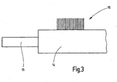
- the gripper device 14 may be provided with a brush 16, in particular from FIG. 3 evident.
- This brush has a number of bristles, which when inserting the workpiece into the tool and / or when leading out in the transport movement to be carried out anyway or thanks to an additional movement to be performed on the embossing relief 9 of the micro-embossing stamp 5 to strip and clean this.
- an optical sensor 17 is integrated into the tool of the embossing device 1 or, as in FIG FIG. 1 illustrated, arranged in the vicinity of the same.
- Light emanating from the sensor or another suitable light source is reflected by the embossed article, eg a freshly embossed coin, and received by the sensor 17, for example by means of an objective 18.
- the sensor also includes an evaluation device which evaluates the image of the diffraction-optically active region recorded by the objective 18. This image can show special color structures or light / dark structures.
- the evaluation device can check color distribution, image contrast and image sharpness.
- the measured values can be reported to a control device 19. This can, for example, track the quality of the coins produced. It can detect quality trends, emit an alarm signal when approaching a lower minimum quality limit and shut down embossing device 1 if the minimum quality limit is not reached. It can also promptly timely or at the latest in case of false production to replace the Mikroticiangestavours 5.
- an embossing tool for the embossing-technical production of structures having a diffractive effect on surfaces of metal objects, in particular coins, which has a stamping body 6 with one on its surface having effective surface provided hard material layer 8.
- the hard material layer In the hard material layer, the negative relief of a diffraction grating is incorporated. This is preferably done by ablation, wherein the relief depth is less than the layer thickness.
- a cleaning device is provided which preferably operates with dry-ice blasting 12, 13. The production-accompanying control of the quality of the embossed diffractogram takes over an optical sensor.
Landscapes
- Physics & Mathematics (AREA)
- General Physics & Mathematics (AREA)
- Engineering & Computer Science (AREA)
- Mechanical Engineering (AREA)
- Shaping Of Tube Ends By Bending Or Straightening (AREA)
- Diffracting Gratings Or Hologram Optical Elements (AREA)
- Adornments (AREA)
Description
- Die Erfindung betrifft eine Vorrichtung und ein Verfahren zum Erzeugen von lichtbeugenden Strukturen an Werkstücken durch Prägen.
- Zur Erzielung farbiger optischer Effekte, wie z.B. Hologramme auf Metalloberflächen, beispielsweise an Münzen, ist es bekannt, die Oberfläche der betreffenden Gegenstände an den gewünschten Stellen mit einer beugungsaktiven Oberflächenstruktur zu versehen. Diese erzeugt Lichtinterferenzen, die den gewünschten optischen Effekt hervorrufen. Beugungsaktive Oberflächen erfüllen dabei nicht nur dekorative Zwecke, sondern können auch dem Schutz vor Fälschung dienen. Die optische Wirkung beruht dabei auf sehr feinen, reliefartig in die jeweilige Oberfläche eingebrachten periodisch aufgebauten Gitterstrukturen. Bekanntestes Beispiel sind metallisierte Kunststofffolien mit Hologrammen, wie sie auf Scheckkarten und Geldscheinen und z.B. bei Klebesiegeln zum Einsatz kommen. Während eine glatte Oberfläche einfallendes Licht reflektiert, d.h. unter einem mit dem Einfallswinkel übereinstimmenden Ausfallswinkel wieder abstrahlt, kommt es an Beugungsgittern zu einer Winkeländerung, die z.B. als Farbumschlageffekt an Hologramm-Folien beobachtet werden kann. Die Herstellung beugungsaktiver Folien beruht auf dem Prägen thermoplastischer Kunststoffe mittels galvanisch geformter Nickelstempel und anschließendem Metallisieren der Gitteroberfläche. Daneben existieren jedoch bereits verschiedene Verfahren, mit denen Beugungsgitter unmittelbar in Obeflächen metallischer Körper eingebracht werden.
- Dazu ist beispielsweise aus der
WO 2004/045866 A1 die Erzeugung solcher Oberflächenstrukturen in Metalloberflächen mittels eines Prägestempels bekannt. Dieser weist Gitter-und/oder Linienstrukturen auf, die sich beim Prägen des Werkstücks an diesem abformen. Dabei wird der Prägestempel durch einen monokristallinen Diamant gebildet, der mittels Kobalt mit einem Trägerkörper verlötet ist. Die Negativstruktur des an dem Werkstück später zu erzeugenden Beugungsgitters wird in den Prägestempel mittels eines Lasers eingearbeitet. Außerdem kann der Prägestempel mit einem Elektronen- oder einem Röntgenstrahl poliert werden. - Bei dieser Vorgehensweise ist die Größe der zu erzeugenden interferenzwirksamen Strukturen von vornherein auf die Größe vorhandener Diamanten begrenzt.
- Des Weiteren offenbart die
DE 100 02 644 A1 die Herstellung beugungswirksamer Reliefstrukturen auf Münzoberflächen. Dazu wird der betreffende Rohling zunächst in einem Tauchbad mit einer dünnen lichtempfindlichen Kunststoffschicht überzogen. Anschließend wird die Kunststoffschicht belichtet und entwickelt. Dadurch werden mikroskopisch feine Stellen der Münzoberfläche frei gelegt. In einem Ätzbad können dann nachfolgend mikroskopische Reliefstrukturen in die Münzoberfläche eingeätzt werden, wonach der fotoempfindliche Kunststoff wieder entfernt wird. DieDE 100 02 644 A1 offenbart darüber hinaus ein Konzept für eine fälschungssichere Münze mit beugungsoptischen, die herkömmlichen Gestaltungselemente einer Münze ergänzenden Merkmalen. Diese sollen visuell erkennbar, aber auch maschinenlesbar sein, wobei die maschinelle Erkennung der beugungsoptischen Signatur auf der Feststellung der räumlichen Lage der Beugungsmaxima beruht. Es wird ein Lesegerät vorgestellt, welches in Münzprüfer und ähnliche Geräte eingebaut ist. Kernstück dieses Lesegeräts ist eine Lichtquelle und eine darauf abgestimmt Sensorik, mit der unter anderem festgestellt wird, ob die Beugungsmaxima des von der Signatur auf der Münze abgestrahlten Lichts an der aufgrund der Wellenlänge des Lichts und der Gitterparameter der Struktur zu erwartenden Stelle auftreten. - Weiter ist aus der
DE 197 22 575 A1 die Herstellung von interferenzfähigen Mikrostrukturen, beispielsweise zur Erzeugung von Hologrammen in Münzen mittels Prägestempel, bekannt. Bei diesem Verfahren werden auf einem Prägestempel mehrere harte Schichten, beispielsweise aus Kobalt-oder Nickellegierungen abgeschieden, in die Diamantkristalle eingelagert sind. Die Schichten können durch spezielle Legierungsbäder oder Metallspritzverfahren, durch galvanische Abscheidung oder durch plasmatische Ablagerung aufgebracht sein. Die Oberflächenschicht wird durch eine diamantähnliche Schicht gebildet, die die Mikrostruktur enthält. Zur Erzeugung der Mikrostrukturen verweist die genannte Schrift allgemein auf galvanische Verfahren, Elektronen- oder Lasergravur, Feinätztechniken und direkte Gravur mittels Diamantwerkzeug. - Aus
EP 0 421 181 A1 ist eine Prägeeinrichtung zur Bearbeitung von Gegenständen bekannt, die einen Mikroprägestempel aufweist. Der Mikroprägestempel weist einen Stempelkörper mit einer zumindest an einer dem Gegenstand zugewandten Seite aufgebrachten Hartstoffschicht auf, die ein Prägerelief zur Erzeugung beugungsaktiver Prägestellen an dem Metallgegenstand aufweist. - Ein Verfahren zur Herstellung eines holografischen Musters ist aus
US 5 372 825 bekannt. Es geht dort um die Erzeugung einer nahtlosen Prägefläche auf einer zylindrischen Walze, mittels der das Muster in eine Folie eingeprägt werden kann. Auf die Walze wird erforderlichenfalls eine prägbare Materialschicht, beispielsweise aus Silber, aufgebracht. Diese Schicht wird gereinigt und geätzt und anschließend werden die Mikrostrukturen mithilfe eines konkaven Stempels eingebracht. Danach kann die Oberfläche poliert oder beschichtet werden. -
DE 197 41 998 A1 beschreibt die Möglichkeit durch Lasergravur hologrammartige Abbildungen an einem Prägewerkzeug anzubringen. - Ausgehend von diesem Stand der Technik ist es Aufgabe der Erfindung, ein praktisch prägestempeltaugliches Verfahren und eine entsprechende Vorrichtung zur prägetechnischen Erzeugung von Beugungsstrukturen von auf Metalloberflächen zu schaffen. Weiterhin ist es Aufgabe der Erfindung, eine praktisch einsetzbare, kostengünstige Produktionstechnik für in Metall geprägte Diffraktogramme zum Einsatz in der Massenfertigung von Umlaufmünzen und Token bzw. Wertmarken, aber auch für die Herstellung z.B. von Sondermünzen und Medaillen anzugeben.
- Diese Aufgabe wird mit den Merkmalen des Anspruchs 1 wie auch den Merkmalen des Anspruchs 16 gelöst.
- Die erfindungsgemäße Prägeeinrichtung enthält ein Prägewerkzeug mit einem in das Prägewerkzeug eingesetzten Stempelkörper, auf den unmittelbar eine Hartstoffschicht aufgebracht ist. Die Hartstoffschicht und der Stempelkörper bilden eine Einheit, wobei die Hartstoffschicht lediglich eine dünne flächige Auflage auf der Oberfläche des Stempelkörpers darstellt. In die Hartstoffschicht ist das gewünschte Prägerelief durch Ablation eingebracht, nachdem die Hartstoffschicht auf den Stempelkörper aufgebracht worden ist. Dies stellt einerseits ein einfach durchführbares Verfahren zur Herstellung der Mikrostrukturen in Form des Prägereliefs dar und stellt andererseits deren Formhaltigkeit auch dann sicher, wenn die Hartstoffschicht relativ dünn ist.
- Ein wesentlicher Aspekt der Erfindung ist der Mikroprägestempel, dessen Grundkörper aus einem hochfesten harten Trägermaterial wie z.B. Hartmetall besteht. Die spätere Bildfläche des Prägestempels weist abgerundete Kanten auf, wodurch beim Prägen Kantenspannungen in der Kontaktzone gemindert und die in der Fläche wirkenden Druckspannungen homogenisiert werden, so dass sich ein gleichmäßiges ebenes Prägebild ergibt. Der Grundkörper wird vorzugsweise durch ein plasma-aktiviertes CVD-Verfahren mit einer z.B. ca. 2 µm dicken, hochelastischen amorphen Schicht aus Kohlenstoff umhüllt. Diese unter der Bezeichnung DLC bekannte Schicht ist, anders als von Korngrenzen durchzogener Stahl, praktisch homogen. Sie ist annähernd so hart wie Diamant, aber ohne dessen Sprödheit und Empfindlichkeit gegenüber Punktbelastung. Sie hat nach außen eine verringerte Adhäsionsneigung, was Prägestempelverschleiß mindert und die Reinigung des Prägestempels erleichtert. Eine beugungsoptische Reliefstruktur kann mittels Laserablation eingebracht werden, wonach unmittelbar, ohne Zwischenschritte zur Härtesteigerung, der fertige Mikroprägestempel zur Verfügung steht. Die Tiefe der Reliefstruktur ist dabei vorzugsweise wesentlich geringer als die Dicke der Hartschicht. Beschränkungen hinsichtlich der Prägestempelgröße ergeben sich lediglich durch das Aufnahmevermögen der zur Beschichtung eingesetzten Anlagen.
- Die durch Laserablation der DLC-Schicht erzeugte Gitterstruktur ist äußerst präzise und scharfkantig ausgeformt. Metallische Oberflächen dagegen zeigen eine geringere Qualität, was auf das Aufschmelzen des Metalls zurückzuführen ist. Ein Vorteil der erfindungsgemäßen Mikroprägestempel liegt in der einfachen Herstellung ohne Zwischenschritte und unter Verwendung gängiger Materialien und Verfahren.
- Das Prägewerkzeug ist vorzugsweise zur Kaltverformung des Metallgegenstands, beispielsweise eines Münzrohlings, eingerichtet. Es ist jedoch alternativ auch möglich, den Prägevorgang an vorgewärmten Rohlingen durchzuführen. Dazu kann der Prägeeinrichtung beispielsweise eine Vorwärmeinrichtung für Münzrohlinge zugeordnet sein.
- Die das Prägerelief bildenden Vertiefungen können punkt- oder linienartige Vertiefungen einheitlicher oder unterschiedlicher Tiefe sein. Sie können außerdem eine einheitliche oder eine unterschiedliche Breite aufweisen. Die Flanken dieser Vertiefungen sind parallel zueinander oder in einem Winkel, beispielsweise in einem spitzen Winkel, zueinander orientiert. Außerdem sind die in die Hartstoffschicht und den Mikroprägestempel eingebrachten Vertiefungen vorzugsweise scharfkantig ausgebildet.
- Als Hartstoffschicht eignen sich sowohl metallische als auch nichtmetallische Hartstoffschichten. Die Hartstoffschichten bestehen z.B. aus zumindest zwei chemischen Elementen. Wie erwähnt werden aber vorzugsweise Diamantschichten oder diamantähnliche Schichten verwendet. Unter metallischen Hartstoffschichten werden Hartstoffschichten mit vorwiegend metallischer Bindung verstanden, wie beispielsweise TiN, TiCN, TiC, TiAlCON, TiBN, wobei die einzelnen Elemente der genannten Verbindungen in verschiedenen Verhältnissen zueinander vorkommen können. An Stelle von Titan kann ganz oder teilweise auch Hafnium oder Zirkon Anwendung finden. Unter nichtmetallischen Hartstoffschichten werden Hartstoffschichten mit vorwiegend kovalenter Bindung verstanden, wie beispielsweise Al2O3 oder Diamantschichten.
- Ein Vorteil der Aufbringung einer Hartstoffschicht auf einen Stempelkörper und die nachfolgende Einbringung des Prägereliefs ist, dass die Interferenzstrukturen sehr klar, scharf bzw. tief zur Verfügung stehen und nicht durch eine nachfolgend aufgetragene Schicht zugedeckt werden.
- Die Erfindung sieht ein Prägestempel-in-Stempel-Verfahren vor, bei dem ein kleinerer, das Negativrelief des Beugungsgitters tragender Zusatzstempel in einen größeren herkömmlichen Prägestempel (Hauptstempel) herausnehmbar eingelassen ist. Wegen des unterschiedlichen Verformungsverhaltens von Hauptstempel und Zusatzstempel bzw. Stützstift ist es zweckmäßig, den Zusatzstempel um wenige Zehntel Millimeter über die Oberfläche des Hauptstempels hinaus stehen zu lassen. Dieses Verfahren ermöglicht a) den unabhängigen Austausch des Zusatzstempels bei Verschleiss oder Verschmutzung, b) die Verwendung unterschiedlicher Werkstoffe, Oberflächenbehandlungen und Beschichtungen für Haupt- und Zusatzstempel und c) das Prägen von Münzen, Medaillen, Token mittels herkömmlicher Münzpräge-, Medaillen- oder Einsenkpressen.
- Darüberhinaus löst die Erfindung ein fertigungstechnisches Kernproblem, das beim Prägen von Beugungsstrukturen in Metalle auftritt. Es besteht darin, dass sich auf den feinen Gitterstrukturen im Mikroprägestempel schon nach wenigen Abprägungen eine Plaque aus Metallabrieb, Oxiden, Staubpartikeln, Schmiermitteln bildet. Diese Plaque behindert das Abprägen des Mikroprägestempel-Reliefs. Eine Vermeidung der Verschmutzung im Prägebetrieb bei der konventionellen Münz- und Medaillenfertigung ist nicht vollständig möglich. Dazu schafft die Erfindung ein effizientes Verfahren zur laufenden automatischen Reinigen der Mikroprägestempel und ermöglicht die Massen- oder Serienfertigung von Münzen.
- Die Erfindung sieht insbesondere zwei integrierte Verfahren zur Reinigung der Diffraktogramm-Mikroprägestempel vor. Zum einen ist dies die Reinigung mittels Trockeneisstrahlen. Dabei wird festes Kohlendioxid in gemahlener bzw. körniger Form mittels Druckluft auf die zu reinigenden Prägestempeloberflächen geblasen. Die Reinigungswirkung ergibt sich durch die kinetische Energie der Trockeneispartikel, durch das Verspröden der Plaques unter Kälteeinfluss, aber auch durch die schlagartige Volumenzunahme beim Kohlendioxid, das bei Aufprall sublimiert und so die Plaqueschicht gewissermaßen sprengt. Das Reinigungsmedium Kohlendioxid entweicht als Gas, die Reste der Plaqueschicht werden dadurch mit entfernt. Vorzugsweise findet dieser Reinigungsvorgang in einer entsprechend modifizierten Münz- oder Medaillenprägemaschine bei laufendem Prägebetrieb statt.
- Eine Ausführungsform der Erfindung besteht darin, dass in Bauteile der Prägemaschine Strahldüsen eingearbeitet sind und eine Synchronisation des Strahlvorgangs mit dem Arbeitstakt der Maschine von der Maschinensteuerung vorgenommen wird. Ein weiterer erfindungsgemäßer Reinigungsmechanismus zur Unterstützung des Trockeneisstrahlens besteht in der Verwendung entsprechend modifizierter Zubringersegmente in einer Prägemaschine mit Revolverzuführung. Die Zubringersegmente dienen der Zuführung der ungeprägten Rohlinge zur Prägestation und übernehmen gleichermaßen den Abtransport der fertig geprägten Münze. Rohlinge und Münzen bewegen sich dabei schrittweise auf einer Kreisbahn. Bei jedem Öffnen der Prägestation durchlaufen die Zubringersegmente den Zwischenraum zwischen den beiden Prägestempeln. Werden die Segmente mit Einsätzen z.B. aus Borsten oder Filz versehen, streichen sie bei jeder Transportbewegung an den Prägestempeln entlang und tragen so die Plaqueschicht teilweise ab. Die Bestückung der Zubringersegmente mit Reinigungseinsätzen muss durch Modifikationen an der Prägemaschine begleitet werden, durch die Platz für die Bewegung der Reinigungseinsätze geschaffen wird.
- Des Weiteren kann nach einer weiteren Ausführungsform der Erfindung der Einsatz von Sensorik zur Steuerung der Produktionsabläufe beim Prägen vorgesehen werden. Es ist damit eine laufende Gut/Schlecht-Prüfung möglich. Verschmutzungen der Diffraktogramm-Mikroprägestempel sind schnell erkennbar. Zum anderen kann die in die Prägemaschine integrierte Sensorik der Feststellung des Lebensdauerendes der Diffraktogramm-Mikroprägestempel dienen. Aufgabe der Sensorik ist dann die Feststellung, ob eine soeben geprägte Münze die gewünschte Beugungsstruktur aufweist und ob die Beugungswirkung noch in hinreichendem Maße gegeben ist.
- Weitere Einzelheiten von vorteilhaften Ausführungsformen der Erfindung ergeben sich aus der Zeichnung, der Beschreibung oder Ansprüchen. Die Beschreibung zeigt wesentliche Merkmale der Erfindung und sonstiger Gegebenheiten. Weitere Einzelheiten entnimmt der Fachmann in gewohnter Weise der Zeichnung.
- Es zeigen:
-
Figur 1 eine Prägeeinrichtung einer Münzprägepresse in schematisierter, längs geschnittener Darstellung, -
Figur 2 einen Mikroprägestempel für die Prägeeinrichtung nachFigur 1 in vergrößerter schematisierter Schnittdarstellung, -
Figur 3 eine Zubringeinrichtung mit Reinigungsbürste für die Prägeeinrichtung nachFigur 1 in vergrößerter schematisierter Darstellung, -
Figur 4 einen Stempelkörper vor Aufbringung der Hartstoffschicht in schematisierter Darstellung, -
Figur 5 den Stempelkörper nach Aufbringen der Hartstoffschicht vor Einbringen des Prägereliefs in schematisierter Darstellung und -
Figur 6 den Stempelkörper mit Hartstoffschicht während der Erzeugung des Prägereliefs durch Ablation in schematisierter Darstellung. - In
Figur 1 ist eine Prägeeinrichtung 1 zum Prägen von Münzen in schematisierter Darstellung veranschaulicht. Zu der Prägeeinrichtung 1 gehören ein unterer Prägestempel 2 und ein zugeordneter oberer Prägestempel 3. Der obere Prägestempel 3 ist in einem Prägering 4 angeordnet. Die Prägestempel 2, 3 sind mit einem nicht weiter veranschaulichten Negativprofil versehen, das beim Prägen einer Münze an deren Oberfläche abgeformt wird. Die Prägestempel 2, 3 bilden somit gegebenenfalls mit dem Prägering 4 jeweils ein Prägewerkzeug. - Die Prägestempel 2, 3 können ein oder mehrere Mikroprägestempel 5 aufweisen, die zur Erzeugung einer fein strukturierten Oberfläche an dem Metallgegenstand, im vorliegenden Fall dem Münzrohling dienen. Die Oberflächenstrukturierung soll dabei so fein sein, dass an der fertig geprägten Münze Beugungs- oder Interferenzerscheinungen auftreten, die zu Farbeffekten oder auch zum Entstehen von Weißlichthologrammen führen.
- Der Mikroprägestempel 5 weist eine Stirnseite auf, die vorzugsweise bündig zu der sonstigen Gravur des Prägewerkzeugs, im vorliegenden Beispiel des Prägestempels 3 angeordnet ist. Der Mikroprägestempel 5 ist vorzugsweise auswechselbar in einer entsprechenden Ausnehmung des Prägewerkzeugs, d.h. des Prägestempels 2, 3, gehalten. Dies hat den Vorzug, dass er bei Verschleiß gewechselt werden kann, wobei der Prägestempel 2, 3 weiter verwendet werden kann. Der Mikroprägestempel 5 ist in einer Bohrung des Prägestempels 2, 3 angeordnet und in dieser mittels eines Stützstifts 6a abgestützt.
- Der Mikroprägestempel 5 ist in
Figur 2 ausschnittsweise gesondert veranschaulicht. Er besteht aus einem im Querschnitt beispielsweise prismatischen oder zylindrischen Stempelkörper 6, der an einer unprofilierten, vorzugsweise ebenen Fläche, beispielsweise seiner Stirnfläche 7, mit einer Hartstoffauflage 8 versehen ist. Die Hartstoffauflage 8 kann sich, wie dargestellt, auf die Stirnfläche 7 beschränken oder alternativ einen größeren Bereich der Oberfläche des Mikroprägestempels 5 einnehmen. Die Hartstoffauflage 8 folgt dabei der Form der Stirnfläche 7. Ist die Stirnfläche 7 eben, so ist auch die Hartstoffschicht 8 eben. Hat die Stirnfläche 7 eine vorgegebene Grundform, wie beispielsweise eine konvexe oder konkave ballige Form, folgt die Hartstoffschicht 8 dieser Form. Die Hartstoffschicht wird vorzugsweise in einem plasma-aktivierten CVD-Verfahren z.B. in Form einer ca. 2 µm dicke amorphen Kohlenstoffschicht hergestellt. Diese unter der Bezeichnung DLC bekannte Schicht ist praktisch homogen und wenig spröde. - Die Hartstoffschicht 8 kann aber beispielsweise auch eine andere, z.B. eine metallische Hartstoffschicht, z.B. eine TiN-oder eine TiAlCNO-Schicht, oder eine nichtmetallische Hartstoffschicht wie beispielsweise eine Al2O3-Schicht sein. Die Hartstoffschicht 8 kann dabei aus einem einzigen Material durchgehend gleicher Struktur bestehen. Es ist jedoch auch möglich, einen Mehrschichtaufbau vorzusehen. Zur Herstellung eignen sich PVD- und/oder CVD-Verfahren.
- In die Hartstoffschicht 8 ist ein Mikro-Prägerelief 9 eingebracht, dessen Strukturierung vorzugsweise im Bereich zwischen 0,1 und 1 µm liegt. Das Prägerelief kann aus einzelnen, zueinander parallelen oder im Winkel zueinander verlaufenden, sich kreuzenden Linien oder auch aus Einzelpunkten bestehen, die Vertiefungen bilden. Das Prägerelief ist in
Figur 2 symbolisch veranschaulicht. Die Vertiefungen weisen vorzugsweise eine Tiefe auf, die geringer ist als die Dicke der Hartstoffschicht 8. Vorzugsweise liegt die Dicke der Hartstoffschicht 8 im Bereich des Zwei- bis Zehnfachen der Tiefe der Vertiefungen. - Vorzugsweise weist der Mikroprägestempel 5 an seiner Stirnseite 7 gerundete Kanten 10 auf, wodurch beim Prägen Kantenspannungen in der Kontaktzone gemindert und die in der Fläche wirkenden Druckspannungen homogenisiert werden. Es ergibt sich ein gleichmäßiges ebenes Prägebild.
- Die Herstellung des Mikroprägestempeles 5 erfolgt gemäß
Figur 4 bis 6 , indem zunächst ein Stempelkörper 6 bereitgestellt wird. Dieser besteht z.B. aus Hartmetall, das pulvermetallurgisch durch Sintern von Rohlingen aus Wolframkarbidpulver mit Zusätzen von Kobalt hergestellt werden kann. Alternativ können Cermets Anwendung finden. Auch kann der Stempelkörper 6 im Metallspritzgießverfahren hergestellt werden, indem ein Hartmetallpulver (z.B. Wolframkarbid mit Kobalt) mit geringen Anteilen von Kunststoff im Spritzgießverfahren zu gewünschten Körpern geformt und danach gesintert wird. Auf den Stempelkörper 6 wird, wie inFigur 5 veranschaulicht, in einem geeigneten Verfahren, beispielsweise PVD, CVD oder einem verwandten Verfahren, die Hartstoffschicht 8 zunächst als gleichmäßig dicke Schicht von wenigen µm Dicke aufgebracht. Diese entsteht somit unmittelbar auf der Stirnfläche 7 und folgt somit der Form dieser Fläche. Nachfolgend wird in einem Ablationsverfahren, beispielsweise in einem Laserablationsverfahren, das gewünschte Prägerelief 9 in die Hartstoffschicht 8 eingebracht. - Der Mikroprägestempel 5 ist nach Fertigstellung des Prägereliefs 9 einsatzfähig. Er wird in den Prägestempel 3 eingesetzt und kann nun ohne weiteres zum Prägen von kalten oder vorgewärmten Ronden zur Münzherstellung dienen.
- Die Prägeeinrichtung 1 ist mit einer in
Figur 1 lediglich symbolisch veranschaulichten Reinigungseinrichtung 11 versehen. Diese dient dazu, die Mikroprägestempel 5 in Betrieb sauber zu halten. Die Säuberung der Mikroprägestempel 5 erfolgt dabei vorzugsweise bei offenem Werkzeug, z.B. durch Trockeneisstrahlen 12, 13. Diese werden durch geeignete, nicht weiter veranschaulichte Düsen auf die Stempel 2, 3 dabei insbesondere auf die Prägereliefs der Mikroprägestempel 5 gerichtet. Die Reinigungswirkung ergibt sich durch mechanische Einwirkung der Trockeneispartikel. Auf den Prägereliefs 9 ausgebildete Plaques oder sonstige Ablagerung verspröden durch die Kälteeinwirkung. Das verdampfende Kohlendioxid sprengt dann die Plaqueschicht ab und bläst deren Bruchstücke aus dem Werkzeug 1. Entsprechende Strahldüsen können bedarfsweise an einem beweglichen Träger angeordnet werden, der bei offenem Werkzeug 1 in dieses hinein taucht. Sodann kann der Trockeneisstrahl freigegeben werden. Es ist auch möglich, entsprechende Reinigungsdüsen an anderen bewegten Maschinenteilen, beispielsweise einer Werkstücktransportvorrichtung anzubringen, die ohnehin in das Werkzeug einfahren muss. Des Weiteren ist es möglich, die zu verformenden Werkstücke, beispielsweise Ronden, vor dem Prägen mit Trockeneis zu reinigen, um Fette oder sonstige Bestandteile zu entfernen. - Der Reinigungsvorgang kann nach jedem Prägevorgang erfolgen. Es ist auch möglich, jeweils eine vorbestimmte Anzahl von Prägevorgängen auszuführen, wonach der Reinigungsvorgang dann ausgeführt wird. Des Weiteren ist es möglich, die Reinigung mittels Trockeneisstrahl lediglich bedarfsweise durchzuführen, wenn beispielsweise eine Verschmutzung der Prägestempel durch einen Abfall der Prägequalität festgestellt wird.
- Zur Erfassung der Prägequalität kann eine Erfassungseinrichtung dienen, die das von dem Prägerelief erzeugte Prägemuster auf einer erzeugten Münze prüft. Dies kann durch Aufstrahlen von Licht und Untersuchung des sich ergebenden Begungsbilds erfolgen.
-
Figur 1 veranschaulicht des Weiteren einen Werkstückgreifer 14 mit Greiferzungen 15, die dazu eingerichtet sind, ein Werkstück aufzunehmen und in die Prägeeinrichtung 1 einzulegen oder aus dieser heraus zu führen. Die Greifereinrichtung 14 kann mit einer Bürste 16 versehen sein, die insbesondere ausFigur 3 hervorgeht. Diese Bürste weist eine Anzahl von Borsten auf, die beim Einlegen des Werkstücks in das Werkzeug und/oder beim Herausführen bei der ohnehin durchzuführenden Transportbewegung oder Dank einer auszuführenden Zusatzbewegung über das Prägerelief 9 des Mikroprägestempels 5 zu streifen und dieses dabei zu reinigen. - Bei einer bevorzugten Ausführungsform ist ein optischer Sensor 17 in das Werkzeug der Prägeeinrichtung 1 integriert oder, wie in
Figur 1 veranschaulicht, in der Nähe desselben angeordnet. Von dem Sensor oder einer anderen geeigneten Lichtquelle ausgehendes Licht wird von dem geprägten Gegenstand, z.B. einer frisch geprägten Münze, reflektiert und von dem Sensor 17 beispielsweise mittels eines Objektivs 18 aufgenommen. Zu dem Sensor gehört außerdem eine Auswerteeinrichtung, die das von dem Objektiv 18 aufgenommene Bild des beugungsoptisch aktiven Bereichs auswertet. Dieses Bild kann spezielle Farbstrukturen oder Hell/Dunkel-Strukturen zeigen. Beispielsweise kann die Auswerteeinrichtung Farbverteilung, Bildkontrast und Bildschärfe prüfen. Die gemessenen Werte können an eine Steuereinrichtung 19 gemeldet werden. Diese kann daran beispielsweise die Qualität der hergestellten Münzen verfolgen. Sie kann Qualitätstrends erkennen, bei Annäherung an eine untere Mindestqualitätsgrenze ein Alarmsignal aussenden und bei Unterschreitung der Mindestqualitätsgrenze die Prägeeinrichtung 1 stillsetzen. Sie kann des Weiteren rechtzeitig oder spätestens bei Fehlproduktion zum Auswechseln des Mikroprägestempels 5 auffordern. - Erfindungsgemäß wird zum prägetechnischen Erzeugen von beugungsoptisch wirksamen Strukturen auf Oberflächen von Metallgegenständen, insbesondere Münzen, ein Prägewerkzeug vorgeschlagen, das einen Stempelkörper 6 mit einer an seiner wirksamen Fläche vorgesehenen Hartstoffschicht 8 aufweist. In die Hartstoffschicht ist das Negativrelief eines Beugungsgitters eingearbeitet. Dies erfolgt vorzugsweise durch Ablation, wobei die Relieftiefe geringer ist als die Schichtdicke. Zum Erhalt der Funktionsfähigkeit des Mikroprägestempels 5 über einen langen Zeitraum ist eine Reinigungseinrichtung vorgesehen, die vorzugsweise mit Trockeneisstrahlen 12, 13 arbeitet. Die produktionsbegleitende Kontrolle der Qualität des abgeprägten Diffraktogramms übernimmt ein optischer Sensor.
-
- 1
- Prägeeinrichtung
- 2
- Stempel
- 3
- Stempel
- 4
- Prägering
- 5
- Mikroprägestempel
- 6
- Stempelkörper 6a Stützstift
- 7
- Stirnfläche
- 8
- Hartstoffschicht
- 9
- Prägerelief
- 10
- Kante
- 11
- Reinigungseinrichtung
- 12
- Trockeneisstrahl
- 13
- Trockeneisstrahl
- 14
- Greifereinrichtung
- 15
- Greiferzungen
- 16
- Bürste
- 17
- Sensor
- 18
- Objektiv
- 19
- Steuereinrichtung
Claims (19)
- Prägeeinrichtung (1) zur Bearbeitung von Gegenständen, insbesondere Metallgegenständen, insbesondere Münzen,
mit einem Prägestempel (2), der ein Bildrelief aufweist und in den ein Mikroprägestempel (5) eingesetzt ist,
wobei der Mikroprägestempel (5) einen Stempelkörper (6) mit einer zumindest an einer dem Gegenstand zugewandten Seite (7) aufgebrachten Hartstoffschicht (8) aufweist, die ein in der Hartstoffschicht (8) auf dem Stempelkörper (6) erzeugtes Prägerelief (9) zur Erzeugung beugungsaktiver Prägestellen an dem Gegenstand aufweist,
und mit einer Reinigungseinrichtung (12, 13) zur Reinigung des Mikroprägestempels (5). - Prägeeinrichtung nach Anspruch 1, dadurch gekennzeichnet, dass der Stempelkörper (6) aus einem hochfesten harten Trägermaterial, vorzugsweise Hartmetall besteht.
- Prägeeinrichtung nach Anspruch 1, dadurch gekennzeichnet, dass der Mikroprägestempel (5) an seiner dem Werkstück zugewandten Seite abgerundete Kanten (10) aufweist.
- Prägeeinrichtung nach Anspruch 1, dadurch gekennzeichnet, dass die Relieftiefe des Mikroprägestempels geringer als die Schichtdicke der Hartstoffschicht (8) ist.
- Prägeeinrichtung nach Anspruch 1, dadurch gekennzeichnet, dass die Hartstoffschicht (8) auf eine unprofilierte, vorzugsweise ebene Fläche (7) des Stempelkörpers (6) aufgebracht ist.
- Prägeeinrichtung nach Anspruch 1, dadurch gekennzeichnet, dass die Hartstoffschicht (8) auf eine profilierte Fläche (7) des Stempelkörpers (6) aufgebracht ist.
- Prägeeinrichtung nach Anspruch 1, dadurch gekennzeichnet, dass die Hartstoffschicht (8) durch ein plasma-aktiviertes CVD-Verfahren auf den Stempelkörper (6) aufgebracht ist.
- Prägeeinrichtung nach Anspruch 1, dadurch gekennzeichnet, dass die Hartstoffschicht (8) eine auf den Stempelkörper (6) aufgebrachte DLC-Schicht ist.
- Prägeeinrichtung nach Anspruch 1, dadurch gekennzeichnet, dass das Prägerelief (9) in die Hartstoffschicht (8) durch Laser-Ablation eingebracht ist.
- Prägeeinrichtung nach Anspruch 1, dadurch gekennzeichnet, dass der Mikroprägestempel (5) in dem Prägestempel (2) herausnehmbar gehalten ist.
- Prägeeinrichtung nach Anspruch 1, dadurch gekennzeichnet, dass die Reinigungseinrichtung eine Partikelstrahlreinigungseinrichtung ist.
- Prägeeinrichtung nach Anspruch 11, dadurch gekennzeichnet, dass die Reinigungseinrichtung Blasdüsen aufweist, mittels derer ein Partikelstrahl auf das Prägerelief (9) des Mikroprägestempels (5) gerichtet werden kann.
- Prägeeinrichtung nach Anspruch 11, dadurch gekennzeichnet, dass die Reinigungseinrichtung Blasdüsen aufweist, die dazu eingerichtet sind, einen Partikelstrahl vor dem Prägevorgang auf das Werkstück zu richten.
- Prägeeinrichtung nach Anspruch 1, dadurch gekennzeichnet, dass die Reinigungseinrichtung eine Bürste (16) aufweist, die dazu eingerichtet ist bei offenem Werkzeug über das Prägerelief (9) zu streichen.
- Prägeeinrichtung nach Anspruch 1, dadurch gekennzeichnet, dass ein optischer Sensor (17) vorgesehen ist, mittels dessen eine Steuereinrichtung (19) die Produktionsqualität überwacht.
- Verfahren zur Herstellung eines Prägewerkzeugs zur Bearbeitung von Gegenständen, insbesondere Metallgegenständen, insbesondere Münzen, mit folgenden Schritten:- Bereitstellen eines Stempelkörpers (6) eines Mikroprägestempels (5) mit einer im Wesentlichen glatten Fläche (7),- Aufbringen einer Hartstoffschicht (8) auf die Fläche (7),- Profilieren der Hartstoffschicht (8) mit einem Ablationsverfahren, wodurch ein Prägerelief (9) zur Erzeugung beugungsaktiver Prägestellen an dem Gegenstand in der Hartstoffschicht (8) erzeugt wird,- Einsetzen des Mikroprägestempels (5) in einen Prägestempel (2) und Sichern des Mikroprägestempels (5) in diesem.
- Verfahren nach Anspruch 16, dadurch gekennzeichnet, dass die Hartstoffschicht in einem PVD-Verfahren, einem CVD-Verfahren oder einer Kombination dieser Verfahren auf den Stempelkörper (6) aufgebracht ist.
- Verfahren nach Anspruch 16, dadurch gekennzeichnet, dass das Ablationsverfahren ein Laser-Ablationsverfahren ist.
- Verfahren nach Anspruch 16, dadurch gekennzeichnet, dass das Ablationsverfahren ein Ätzverfahren ist.
Applications Claiming Priority (1)
| Application Number | Priority Date | Filing Date | Title |
|---|---|---|---|
| DE102006052511A DE102006052511B3 (de) | 2006-11-06 | 2006-11-06 | Prägeeinrichtung und Verfahren zur Herstellung eines Prägewerkzeugs |
Publications (3)
| Publication Number | Publication Date |
|---|---|
| EP1918125A2 EP1918125A2 (de) | 2008-05-07 |
| EP1918125A3 EP1918125A3 (de) | 2011-08-31 |
| EP1918125B1 true EP1918125B1 (de) | 2014-01-22 |
Family
ID=38982732
Family Applications (1)
| Application Number | Title | Priority Date | Filing Date |
|---|---|---|---|
| EP07019599.5A Not-in-force EP1918125B1 (de) | 2006-11-06 | 2007-10-08 | Prägeeinrichtung und Verfahren zur Herstellung eines Prägewerkzeugs |
Country Status (2)
| Country | Link |
|---|---|
| EP (1) | EP1918125B1 (de) |
| DE (1) | DE102006052511B3 (de) |
Cited By (1)
| Publication number | Priority date | Publication date | Assignee | Title |
|---|---|---|---|---|
| CN111332054A (zh) * | 2020-03-17 | 2020-06-26 | 南京俊达诚数控科技有限公司 | 一种用于木质板材加工的具有清洁功能的压纹设备 |
Families Citing this family (8)
| Publication number | Priority date | Publication date | Assignee | Title |
|---|---|---|---|---|
| DE102009021880B4 (de) * | 2009-05-19 | 2013-01-31 | Schuler Pressen Gmbh & Co. Kg | Prägeverfahren und Prägeeinrichtung zur Erzeugung beugungswirksamer Strukturen |
| WO2012129691A1 (en) | 2011-03-28 | 2012-10-04 | Monnaie Royale Canadienne / Royal Canadian Mint | System and method for reducing giveaway material on mint products |
| DE102014111245A1 (de) * | 2014-08-07 | 2016-02-11 | Reischauer Gmbh | Verfahren zum Herstellen eines Prägerohlings für Münzen und Medaillen, Prägerohling und Verwendung des Prägerohlings |
| DE102016110403A1 (de) * | 2016-06-06 | 2017-12-07 | THB Treuhandholding und Beteiligungsgesellschaft UG (hb) | Verfahren zur Herstellung eines Prägewerkzeugs sowie Prägewerkzeug |
| DE102017007900B3 (de) | 2017-08-19 | 2018-11-29 | Sack & Kiesselbach Maschinenfabrik Gmbh | Vorrichtung und Verfahren zum Prägen von Münzen oder Medaillen |
| DE102017010913B3 (de) | 2017-11-25 | 2019-01-24 | Sack & Kiesselbach Maschinenfabrik Gmbh | Verfahren zum Betreiben einer Prägevorrichtung und Prägevorrichtung |
| RU2664141C1 (ru) * | 2018-01-24 | 2018-08-15 | Акционерное общество "Гознак" (АО "Гознак") | Устройство для изготовления композиционного изделия (варианты) и изделие, полученное при помощи этого устройства |
| DE102020103614B4 (de) | 2020-02-12 | 2023-05-11 | Bundesdruckerei Gmbh | Belichtungstisch für eine hologrammbelichtungsmaschine |
Family Cites Families (9)
| Publication number | Priority date | Publication date | Assignee | Title |
|---|---|---|---|---|
| CH681366A5 (de) * | 1989-10-04 | 1993-03-15 | Pamp S A | |
| DE4314410C2 (de) * | 1993-05-03 | 1996-11-28 | Land Baden Wuerttemberg Staatl | Prägewerkzeug zur Herstellung von Münzen, Medaillen oder Marken |
| US5327825A (en) * | 1993-05-12 | 1994-07-12 | Transfer Print Foils, Inc. | Seamless holographic transfer |
| US5471923A (en) * | 1994-12-19 | 1995-12-05 | Chrysler Corporation | Multiple stamping dies with cumulative stamping markers and method of stampings parts |
| DE19722575A1 (de) * | 1997-05-29 | 1998-12-03 | Matthiesen Miriam | Verfahren zum Einprägen von Mikrostrukturen in Metalle oder andere Hartstoffe |
| DE19741998A1 (de) * | 1997-09-24 | 1999-03-25 | Baublys Gmbh | Verfahren zum Herstellen und/oder Bearbeiten eines Prägewerkzeugs für Münzen oder Medaillen |
| DE10002644A1 (de) * | 2000-01-21 | 2001-08-16 | Ovd Kinegram Ag Zug | Münze mit Beugungsstrukturen |
| JP4570958B2 (ja) * | 2002-11-16 | 2010-10-27 | フェレンベルク シュテファン | ナノ光学カラーエンボスの方法及び装置 |
| NL1025511C2 (nl) * | 2004-02-18 | 2005-08-19 | Konink Nl Munt N V | Werkwijze voor het op een munt/penning aanbrengen van een afbeelding, zo verkregen munt/penning alsmede daarvoor gebruikte matrijs. |
-
2006
- 2006-11-06 DE DE102006052511A patent/DE102006052511B3/de not_active Expired - Fee Related
-
2007
- 2007-10-08 EP EP07019599.5A patent/EP1918125B1/de not_active Not-in-force
Cited By (2)
| Publication number | Priority date | Publication date | Assignee | Title |
|---|---|---|---|---|
| CN111332054A (zh) * | 2020-03-17 | 2020-06-26 | 南京俊达诚数控科技有限公司 | 一种用于木质板材加工的具有清洁功能的压纹设备 |
| CN111332054B (zh) * | 2020-03-17 | 2022-06-14 | 南京尊豪家具有限公司 | 一种用于木质板材加工的具有清洁功能的压纹设备 |
Also Published As
| Publication number | Publication date |
|---|---|
| DE102006052511B3 (de) | 2008-07-31 |
| EP1918125A3 (de) | 2011-08-31 |
| EP1918125A2 (de) | 2008-05-07 |
Similar Documents
| Publication | Publication Date | Title |
|---|---|---|
| EP1918125A2 (de) | Prägeeinrichtung und Verfahren zur Herstellung eines Prägewerkzeugs | |
| DE102009021880B4 (de) | Prägeverfahren und Prägeeinrichtung zur Erzeugung beugungswirksamer Strukturen | |
| EP1629994B1 (de) | Verfahren zur Herstellung eines Prägeblechs mit dreidimensionaler Struktur zur Herstellung von Dokumenten mittels Heiss-Kalt-Laminierpresse | |
| EP1609588B1 (de) | Vorrichtung und Verfahren zum Satinieren und Prägen von Flachmaterial | |
| DE102009036648A1 (de) | Verfahren zum Herstellen eines dreidimensional geformten Gegenstands | |
| EP1437213A1 (de) | Vorrichtung zum Satinieren und Prägen von Flachmaterial | |
| JPH0613125B2 (ja) | 圧延方法、圧延製品、圧延ロールおよび板製品 | |
| EP2327503A1 (de) | Verfahren und Vorrichtung zur Strukturierung einer mit einer Hartstoff-Beschichtung versehenen Festkörper-Oberfläche mit einem Nanosekundenbereich-Pulslängen erzeugenden Laser und mit einem zweiten Piko- oder Femetosekundenbereich-Pulslängen erzeugenden Laser | |
| WO2003057494A1 (de) | Stahltiefdruckverfahren zum herstellen eines sicherheitsdokuments sowie stahltiefdruckplatte und halbzeuge dafür und verfahren zu deren herstellung | |
| WO2016142005A1 (de) | Galvanisch dekoriertes bauteil aus kunststoff sowie verfahren zur herstellung eines kunststoffbauteils mit strukturierter oberfläche | |
| EP3834653B1 (de) | Münze oder medaille | |
| EP3900944B1 (de) | Verfahren zum markieren mittels laserpulsen | |
| Braun et al. | Nanoscale patterning of metallic surfaces with laser patterned tools using a nanoimprinting approach | |
| EP1597088A1 (de) | Nanooptisches farbpr gen | |
| DE102009004379A1 (de) | Verfahren, Verwendung, Herstellungsgerät und Computerprogrammprodukt | |
| US10017957B1 (en) | Method for manufacturing door lever | |
| EP2147730B1 (de) | Verfahren zum Aufbringen einer Oberflächenstruktur auf einen Festkörper und dessen Verwendung | |
| Guo | Effect of Irradiation Parameters on Morphology of Polishing DF2 (AISI‐O1) Surface by Nd: YAG Laser | |
| EP1866164B1 (de) | Verfahren zum aufbringen eines metallelementes auf ein sicherheitsdokument | |
| EP2580071A1 (de) | Verfahren zum strukturieren von körpern | |
| EP0086507A2 (de) | Verfahren zur Herstellung codierter Münzen | |
| EP4373663B1 (de) | Presswerkzeug und verfahren zum herstellen eines pressblechs | |
| CH712568A1 (de) | Applik zur Montage auf einem Zifferblatt. | |
| Aizawa et al. | Micro-/Nano-Texturing onto Plasma-Nitrided Tool Surface by Laser Printing for CNC Imprinting and Piercing. Micromachines 2022, 13, 265 | |
| EP3739113A1 (de) | Verfahren und vorrichtung zum herstellen eines wasserzeichen-werkzeugs |
Legal Events
| Date | Code | Title | Description |
|---|---|---|---|
| PUAI | Public reference made under article 153(3) epc to a published international application that has entered the european phase |
Free format text: ORIGINAL CODE: 0009012 |
|
| AK | Designated contracting states |
Kind code of ref document: A2 Designated state(s): AT BE BG CH CY CZ DE DK EE ES FI FR GB GR HU IE IS IT LI LT LU LV MC MT NL PL PT RO SE SI SK TR |
|
| AX | Request for extension of the european patent |
Extension state: AL BA HR MK RS |
|
| PUAL | Search report despatched |
Free format text: ORIGINAL CODE: 0009013 |
|
| AK | Designated contracting states |
Kind code of ref document: A3 Designated state(s): AT BE BG CH CY CZ DE DK EE ES FI FR GB GR HU IE IS IT LI LT LU LV MC MT NL PL PT RO SE SI SK TR |
|
| AX | Request for extension of the european patent |
Extension state: AL BA HR MK RS |
|
| RIC1 | Information provided on ipc code assigned before grant |
Ipc: G03H 1/02 20060101ALI20110725BHEP Ipc: B44B 5/02 20060101AFI20110725BHEP Ipc: A44C 21/00 20060101ALI20110725BHEP |
|
| 17P | Request for examination filed |
Effective date: 20120210 |
|
| AKX | Designation fees paid |
Designated state(s): AT BE BG CH CY CZ DE DK EE ES FI FR GB GR HU IE IS IT LI LT LU LV MC MT NL PL PT RO SE SI SK TR |
|
| 17Q | First examination report despatched |
Effective date: 20121212 |
|
| GRAP | Despatch of communication of intention to grant a patent |
Free format text: ORIGINAL CODE: EPIDOSNIGR1 |
|
| INTG | Intention to grant announced |
Effective date: 20131018 |
|
| GRAS | Grant fee paid |
Free format text: ORIGINAL CODE: EPIDOSNIGR3 |
|
| GRAA | (expected) grant |
Free format text: ORIGINAL CODE: 0009210 |
|
| RAP1 | Party data changed (applicant data changed or rights of an application transferred) |
Owner name: SCHULER PRESSEN GMBH |
|
| AK | Designated contracting states |
Kind code of ref document: B1 Designated state(s): AT BE BG CH CY CZ DE DK EE ES FI FR GB GR HU IE IS IT LI LT LU LV MC MT NL PL PT RO SE SI SK TR |
|
| REG | Reference to a national code |
Ref country code: GB Ref legal event code: FG4D Free format text: NOT ENGLISH |
|
| REG | Reference to a national code |
Ref country code: CH Ref legal event code: EP |
|
| REG | Reference to a national code |
Ref country code: AT Ref legal event code: REF Ref document number: 650600 Country of ref document: AT Kind code of ref document: T Effective date: 20140215 |
|
| REG | Reference to a national code |
Ref country code: IE Ref legal event code: FG4D Free format text: LANGUAGE OF EP DOCUMENT: GERMAN |
|
| REG | Reference to a national code |
Ref country code: DE Ref legal event code: R096 Ref document number: 502007012719 Country of ref document: DE Effective date: 20140306 |
|
| REG | Reference to a national code |
Ref country code: NL Ref legal event code: VDEP Effective date: 20140122 |
|
| REG | Reference to a national code |
Ref country code: LT Ref legal event code: MG4D |
|
| PG25 | Lapsed in a contracting state [announced via postgrant information from national office to epo] |
Ref country code: IS Free format text: LAPSE BECAUSE OF FAILURE TO SUBMIT A TRANSLATION OF THE DESCRIPTION OR TO PAY THE FEE WITHIN THE PRESCRIBED TIME-LIMIT Effective date: 20140522 Ref country code: LT Free format text: LAPSE BECAUSE OF FAILURE TO SUBMIT A TRANSLATION OF THE DESCRIPTION OR TO PAY THE FEE WITHIN THE PRESCRIBED TIME-LIMIT Effective date: 20140122 |
|
| PG25 | Lapsed in a contracting state [announced via postgrant information from national office to epo] |
Ref country code: SE Free format text: LAPSE BECAUSE OF FAILURE TO SUBMIT A TRANSLATION OF THE DESCRIPTION OR TO PAY THE FEE WITHIN THE PRESCRIBED TIME-LIMIT Effective date: 20140122 Ref country code: ES Free format text: LAPSE BECAUSE OF FAILURE TO SUBMIT A TRANSLATION OF THE DESCRIPTION OR TO PAY THE FEE WITHIN THE PRESCRIBED TIME-LIMIT Effective date: 20140122 Ref country code: NL Free format text: LAPSE BECAUSE OF FAILURE TO SUBMIT A TRANSLATION OF THE DESCRIPTION OR TO PAY THE FEE WITHIN THE PRESCRIBED TIME-LIMIT Effective date: 20140122 Ref country code: FI Free format text: LAPSE BECAUSE OF FAILURE TO SUBMIT A TRANSLATION OF THE DESCRIPTION OR TO PAY THE FEE WITHIN THE PRESCRIBED TIME-LIMIT Effective date: 20140122 Ref country code: CY Free format text: LAPSE BECAUSE OF FAILURE TO SUBMIT A TRANSLATION OF THE DESCRIPTION OR TO PAY THE FEE WITHIN THE PRESCRIBED TIME-LIMIT Effective date: 20140122 Ref country code: PT Free format text: LAPSE BECAUSE OF FAILURE TO SUBMIT A TRANSLATION OF THE DESCRIPTION OR TO PAY THE FEE WITHIN THE PRESCRIBED TIME-LIMIT Effective date: 20140522 |
|
| PG25 | Lapsed in a contracting state [announced via postgrant information from national office to epo] |
Ref country code: LV Free format text: LAPSE BECAUSE OF FAILURE TO SUBMIT A TRANSLATION OF THE DESCRIPTION OR TO PAY THE FEE WITHIN THE PRESCRIBED TIME-LIMIT Effective date: 20140122 |
|
| REG | Reference to a national code |
Ref country code: DE Ref legal event code: R097 Ref document number: 502007012719 Country of ref document: DE |
|
| PG25 | Lapsed in a contracting state [announced via postgrant information from national office to epo] |
Ref country code: DK Free format text: LAPSE BECAUSE OF FAILURE TO SUBMIT A TRANSLATION OF THE DESCRIPTION OR TO PAY THE FEE WITHIN THE PRESCRIBED TIME-LIMIT Effective date: 20140122 Ref country code: EE Free format text: LAPSE BECAUSE OF FAILURE TO SUBMIT A TRANSLATION OF THE DESCRIPTION OR TO PAY THE FEE WITHIN THE PRESCRIBED TIME-LIMIT Effective date: 20140122 Ref country code: RO Free format text: LAPSE BECAUSE OF FAILURE TO SUBMIT A TRANSLATION OF THE DESCRIPTION OR TO PAY THE FEE WITHIN THE PRESCRIBED TIME-LIMIT Effective date: 20140122 Ref country code: CZ Free format text: LAPSE BECAUSE OF FAILURE TO SUBMIT A TRANSLATION OF THE DESCRIPTION OR TO PAY THE FEE WITHIN THE PRESCRIBED TIME-LIMIT Effective date: 20140122 |
|
| PG25 | Lapsed in a contracting state [announced via postgrant information from national office to epo] |
Ref country code: SK Free format text: LAPSE BECAUSE OF FAILURE TO SUBMIT A TRANSLATION OF THE DESCRIPTION OR TO PAY THE FEE WITHIN THE PRESCRIBED TIME-LIMIT Effective date: 20140122 Ref country code: PL Free format text: LAPSE BECAUSE OF FAILURE TO SUBMIT A TRANSLATION OF THE DESCRIPTION OR TO PAY THE FEE WITHIN THE PRESCRIBED TIME-LIMIT Effective date: 20140122 |
|
| PLBE | No opposition filed within time limit |
Free format text: ORIGINAL CODE: 0009261 |
|
| STAA | Information on the status of an ep patent application or granted ep patent |
Free format text: STATUS: NO OPPOSITION FILED WITHIN TIME LIMIT |
|
| 26N | No opposition filed |
Effective date: 20141023 |
|
| REG | Reference to a national code |
Ref country code: DE Ref legal event code: R097 Ref document number: 502007012719 Country of ref document: DE Effective date: 20141023 |
|
| PG25 | Lapsed in a contracting state [announced via postgrant information from national office to epo] |
Ref country code: MC Free format text: LAPSE BECAUSE OF FAILURE TO SUBMIT A TRANSLATION OF THE DESCRIPTION OR TO PAY THE FEE WITHIN THE PRESCRIBED TIME-LIMIT Effective date: 20140122 Ref country code: SI Free format text: LAPSE BECAUSE OF FAILURE TO SUBMIT A TRANSLATION OF THE DESCRIPTION OR TO PAY THE FEE WITHIN THE PRESCRIBED TIME-LIMIT Effective date: 20140122 Ref country code: LU Free format text: LAPSE BECAUSE OF FAILURE TO SUBMIT A TRANSLATION OF THE DESCRIPTION OR TO PAY THE FEE WITHIN THE PRESCRIBED TIME-LIMIT Effective date: 20141008 |
|
| REG | Reference to a national code |
Ref country code: CH Ref legal event code: PL |
|
| PG25 | Lapsed in a contracting state [announced via postgrant information from national office to epo] |
Ref country code: BE Free format text: LAPSE BECAUSE OF NON-PAYMENT OF DUE FEES Effective date: 20141031 |
|
| REG | Reference to a national code |
Ref country code: IE Ref legal event code: MM4A |
|
| PG25 | Lapsed in a contracting state [announced via postgrant information from national office to epo] |
Ref country code: CH Free format text: LAPSE BECAUSE OF NON-PAYMENT OF DUE FEES Effective date: 20141031 Ref country code: LI Free format text: LAPSE BECAUSE OF NON-PAYMENT OF DUE FEES Effective date: 20141031 |
|
| REG | Reference to a national code |
Ref country code: FR Ref legal event code: ST Effective date: 20150630 |
|
| PG25 | Lapsed in a contracting state [announced via postgrant information from national office to epo] |
Ref country code: FR Free format text: LAPSE BECAUSE OF NON-PAYMENT OF DUE FEES Effective date: 20141031 |
|
| PG25 | Lapsed in a contracting state [announced via postgrant information from national office to epo] |
Ref country code: IE Free format text: LAPSE BECAUSE OF NON-PAYMENT OF DUE FEES Effective date: 20141008 |
|
| REG | Reference to a national code |
Ref country code: AT Ref legal event code: MM01 Ref document number: 650600 Country of ref document: AT Kind code of ref document: T Effective date: 20141008 |
|
| PG25 | Lapsed in a contracting state [announced via postgrant information from national office to epo] |
Ref country code: AT Free format text: LAPSE BECAUSE OF NON-PAYMENT OF DUE FEES Effective date: 20141008 |
|
| PG25 | Lapsed in a contracting state [announced via postgrant information from national office to epo] |
Ref country code: BG Free format text: LAPSE BECAUSE OF FAILURE TO SUBMIT A TRANSLATION OF THE DESCRIPTION OR TO PAY THE FEE WITHIN THE PRESCRIBED TIME-LIMIT Effective date: 20140122 |
|
| PG25 | Lapsed in a contracting state [announced via postgrant information from national office to epo] |
Ref country code: GR Free format text: LAPSE BECAUSE OF FAILURE TO SUBMIT A TRANSLATION OF THE DESCRIPTION OR TO PAY THE FEE WITHIN THE PRESCRIBED TIME-LIMIT Effective date: 20140423 Ref country code: IT Free format text: LAPSE BECAUSE OF FAILURE TO SUBMIT A TRANSLATION OF THE DESCRIPTION OR TO PAY THE FEE WITHIN THE PRESCRIBED TIME-LIMIT Effective date: 20140122 |
|
| PG25 | Lapsed in a contracting state [announced via postgrant information from national office to epo] |
Ref country code: TR Free format text: LAPSE BECAUSE OF FAILURE TO SUBMIT A TRANSLATION OF THE DESCRIPTION OR TO PAY THE FEE WITHIN THE PRESCRIBED TIME-LIMIT Effective date: 20140122 Ref country code: MT Free format text: LAPSE BECAUSE OF FAILURE TO SUBMIT A TRANSLATION OF THE DESCRIPTION OR TO PAY THE FEE WITHIN THE PRESCRIBED TIME-LIMIT Effective date: 20140122 Ref country code: HU Free format text: LAPSE BECAUSE OF FAILURE TO SUBMIT A TRANSLATION OF THE DESCRIPTION OR TO PAY THE FEE WITHIN THE PRESCRIBED TIME-LIMIT; INVALID AB INITIO Effective date: 20071008 |
|
| PGFP | Annual fee paid to national office [announced via postgrant information from national office to epo] |
Ref country code: DE Payment date: 20180917 Year of fee payment: 12 |
|
| PGFP | Annual fee paid to national office [announced via postgrant information from national office to epo] |
Ref country code: GB Payment date: 20181025 Year of fee payment: 12 |
|
| REG | Reference to a national code |
Ref country code: DE Ref legal event code: R119 Ref document number: 502007012719 Country of ref document: DE |
|
| PG25 | Lapsed in a contracting state [announced via postgrant information from national office to epo] |
Ref country code: DE Free format text: LAPSE BECAUSE OF NON-PAYMENT OF DUE FEES Effective date: 20200501 |
|
| GBPC | Gb: european patent ceased through non-payment of renewal fee |
Effective date: 20191008 |
|
| PG25 | Lapsed in a contracting state [announced via postgrant information from national office to epo] |
Ref country code: GB Free format text: LAPSE BECAUSE OF NON-PAYMENT OF DUE FEES Effective date: 20191008 |