EP1914884A1 - Delay regulating device - Google Patents
Delay regulating device Download PDFInfo
- Publication number
- EP1914884A1 EP1914884A1 EP05767437A EP05767437A EP1914884A1 EP 1914884 A1 EP1914884 A1 EP 1914884A1 EP 05767437 A EP05767437 A EP 05767437A EP 05767437 A EP05767437 A EP 05767437A EP 1914884 A1 EP1914884 A1 EP 1914884A1
- Authority
- EP
- European Patent Office
- Prior art keywords
- delay
- signal
- amount
- error
- correlation value
- Prior art date
- Legal status (The legal status is an assumption and is not a legal conclusion. Google has not performed a legal analysis and makes no representation as to the accuracy of the status listed.)
- Granted
Links
Images





Classifications
-
- H—ELECTRICITY
- H03—ELECTRONIC CIRCUITRY
- H03F—AMPLIFIERS
- H03F1/00—Details of amplifiers with only discharge tubes, only semiconductor devices or only unspecified devices as amplifying elements
- H03F1/32—Modifications of amplifiers to reduce non-linear distortion
-
- H—ELECTRICITY
- H03—ELECTRONIC CIRCUITRY
- H03F—AMPLIFIERS
- H03F1/00—Details of amplifiers with only discharge tubes, only semiconductor devices or only unspecified devices as amplifying elements
- H03F1/32—Modifications of amplifiers to reduce non-linear distortion
- H03F1/3241—Modifications of amplifiers to reduce non-linear distortion using predistortion circuits
- H03F1/3247—Modifications of amplifiers to reduce non-linear distortion using predistortion circuits using feedback acting on predistortion circuits
-
- H—ELECTRICITY
- H03—ELECTRONIC CIRCUITRY
- H03F—AMPLIFIERS
- H03F1/00—Details of amplifiers with only discharge tubes, only semiconductor devices or only unspecified devices as amplifying elements
- H03F1/32—Modifications of amplifiers to reduce non-linear distortion
- H03F1/3241—Modifications of amplifiers to reduce non-linear distortion using predistortion circuits
- H03F1/3294—Acting on the real and imaginary components of the input signal
-
- H—ELECTRICITY
- H03—ELECTRONIC CIRCUITRY
- H03F—AMPLIFIERS
- H03F2201/00—Indexing scheme relating to details of amplifiers with only discharge tubes, only semiconductor devices or only unspecified devices as amplifying elements covered by H03F1/00
- H03F2201/32—Indexing scheme relating to modifications of amplifiers to reduce non-linear distortion
- H03F2201/3233—Adaptive predistortion using lookup table, e.g. memory, RAM, ROM, LUT, to generate the predistortion
Definitions
- the present invention relates to a delay regulating device for a reference signal and a feedback signal in an adaptive predistorter (APD) type distortion compensation device.
- APD adaptive predistorter
- FIG. 1 is a block diagram of a transmission board to which the distortion compensation in the APD system is applied.
- the reference signal (Ref signal) is a baseband signal of a transmission signal.
- the reference signal is input to a multiplier 10, multiplied by a distortion compensation coefficient from a distortion compensation control unit 15, and input to a D/A converter 11.
- a modulator 12 modulates the signal, and a power amplifier 12 amplifies and transmits the signal.
- the modulator receives a radio frequency for up-conversion from a local oscillator 14.
- a reference signal is input to the distortion compensation control unit 15.
- the reference signal input to the distortion compensation control unit 15 is used to index a distortion compensation table.
- the reference signal is input to a clock unit delay unit 16.
- the reference signal is delayed by the clock unit delay unit 16 in a clock unit, and input to an adder 17 and a correlation calculating unit 18.
- the clock of the clock unit delay unit 16 is controlled by the correlation calculating unit 18, and an amount of delay by the clock unit delay unit 16 is controlled by controlling the clock.
- the signal output from the power amplifier 12 is input to a multiplier 23 as a feedback signal (FB signal).
- the multiplier 23 multiplies the signal by a radio frequency from a local oscillator 24 for down-conversion.
- the output of the multiplier 23 is input to an A/D converter 22, and converted from an analog signal into a digital signal.
- the feedback signal converted into a digital signal is demodulated by a demodulator 21, and input to a delay filter 20.
- the delay filter 20 is typically a FIR filter, and can change the amount of delay of a signal by changing a tap coefficient.
- the output of the delay filter 20 is input to a negative terminal of the adder 17 and the correlation calculating unit 18.
- the correlation calculating unit 18 controls the phase of an oscillated wave of a numerical control oscillator 25 for inputting a periodical wave to the demodulator 21.
- the correlation calculating unit 18 calculates a correlation value between the reference signal and the feedback signal, and controls the clock unit delay unit 16 and the numerical control oscillator 25 such that the correlation value can be higher.
- the adder 17 obtains a difference between the reference signal input to the adder 17 and the feedback signal input to the negative terminal of the adder 17, and inputs the result to the distortion compensation control unit 15 and an error calculating unit 19.
- the error calculating unit 19 adjusts the amount of delay of the delay filter 20 such that the output of the adder 17 can be lower.
- An error signal as output of the adder 17 is used for update of a distortion compensation coefficient of a distortion compensation table stored in the distortion compensation control unit 15.
- the conventional adjustment of a relative amount of delay between a feedback signal and a reference signal is performed in the following two steps.
- step (1) above a reference signal is delayed in a clock unit, and an amount of delay for the maximum correlation value between the reference signal and the feedback signal is calculated.
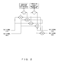
- FIG. 2 shows the circuit for performing the correlation calculation.
- the reference signal and the feedback signal are complex signals each of the signals includes an I signal and a Q signal.
- the I signal of the reference signal is Ref_ich
- the Q signal of the reference signal is Ref_qch
- the I signal of the feedback signal is FB_ich
- the Q signal of the feedback signal is FB_qch
- a correlation result real part integrator and a correlation result imaginary part integrator perform multiplication on a plurality of calculation results of a real part and an imaginary part of an obtained correlation value, and perform a calculation of a sum of the equations above.
- FIG. 3 shows an example of a result of a correlation calculation.
- FIG. 3 shows an example of a result of calculation of a correlation value by assigning various amounts of delay to a reference signal in a clock unit.
- a correlation value shows peaks at various amounts of delay, and shows the maximum peak value when the relative delay between the reference signal and the feedback signal shows the minimum value. Therefore, by detecting the amount of delay indicating the maximum peak value of the correlation value, the timing between the reference signal and the feedback signal can be detected.
- the amount of delay in a clock unit obtained in step (1) above is set.
- the correlation calculating unit 18 adjusts the phase of the demodulator 21 on the basis of the set delay.
- the correlation calculating unit 18 performs the phase adjustment of the demodulator 21 by calculating a phase value as follows.
- a phase value indicating the shift of the phase by the relative delay between the feedback signal and the reference signal can be acquired.
- the phase adjustment is performed to eliminate the phase difference between the reference signal and the feedback signal when the error calculation is performed in the delay regulation in step (2) above.
- the delay of the feedback signal is changed using a digital filter (delay filter).
- a tap coefficient for delay in 1/128 clock unit is prepared for the delay filter.
- FIGS. 4A and 4B explain a digital filter.
- a digital filter is specifically a FIR filter.
- the digital filter includes a plurality of serially connected delay units, each multiplier for multiplying the output of each delay unit by a tap coefficient A0 ⁇ An, and an adder for adding up the output of each multiplier and outputting a result.
- 128 delay units are provided to generate a delay in 1/128 clock unit. The delay value of each delay is 128 clocks.
- FIG. 4B shows an example of a tap coefficient, and is a plot having a vertical axis indicating the value of each tap coefficient when there are 11 taps.
- FIG. 5 shows an example of a circuit for performing an error calculation
- FIG. 6 shows an example of an error calculation result.
- the name of each variable is the same as that in the description of the correlation calculation.
- the error result real part integrator and the error result imaginary part integrator obtain a sum of the real part and the imaginary part of the error value.
- FIG. 6 shows an amount of delay of a feedback signal in 1/128 clock unit along a horizontal axis, and shows an error value along the vertical axis.
- the amount of delay indicating the minimum error value is the optimum amount of delay.
- phase adjustment of the demodulator at the preceding stage of the error calculation in step (2) above is performed using the optimum point of the clock obtained in step (1) above and an initial value delay filter (initial value (0) in 1/128 clock unit), but there is the possibility that the filter tap coefficient of the optimum delay point is different from the delay filter tap coefficient of the initial value.
- the phase adj ustment is performed with a shifted delay, a correct phase cannot be obtained, thereby failing in obtaining a correct tap coefficient.
- FIG. 7 shows the phase adjustment result of the demodulator using a tap coefficient (delay value)
- FIG. 8 shows variations of the delay regulation results of the error calculation.
- FIG. 7 shows along the horizontal axis the number of times of performing the phase adjusting process, and shows along the vertical axis a change in phase value.
- the graph shows the three cases of set values of 0, 128, and 64 of the amount of delay in 1/128 clock unit. As shown by the graph, unless the tap coefficient of the delay filter is appropriate, the phase value is not close to 0 although the phase adjusting process is repeated many times.
- FIG. 8 shows the case in which a delay regulation is performed using a delay filter on the basis of a result of the error calculation.
- FIG. 8 shows a result of repeating the trial delay regulation several times, and the graphs using different marks refer to different trials. As shown in FIG. 8 , each time trial delay regulation is performed, a different amount of delay brings about the minimum error result, and the optimum reliable amount of delay cannot be obtained only by the delay regulation using an error result.
- the conventional distortion compensation device can be the patent document 1.
- the patent document 1 discloses a technique of not updating a distortion compensation table when a phase value is abnormal.
- Patent Document 1 International Patent Application Publication No. WO 03/103166
- the present invention aims at providing a delay regulating device capable of setting the timing of a reference signal and a feedback signal as a reliable and optimum value, and updating a correct distortion compensation coefficient.
- the delay regulating device is used in a distortion compensation device for calculating an error signal between a first signal and a second signal and updating a distortion compensation coefficient from the error signal, and adjusts an amount of delay of the first signal and the second signal.
- the delay regulating device includes: a correlation value calculation device calculating a correlation value between the first signal and the second signal; an error signal calculation device calculating an error signal between the first signal and the second signal; a first delay device adjusting a relative amount of delay between the first signal and the second signal; a second delay device adjusting the relative amount of delay between the first signal and the second signal in a unit smaller than the first delay device; and a control device first setting using the first delay device the relative amount of delay such that the correlation value is maximum, second adjusting using the second delay device the relative amount of delay such that the correlation value is maximum, and third readjusting using the second delay device the relative amount of delay such that the error signal is minimum.
- the delay regulation is performed in the following procedure to solve the above-mentioned problem.
- the delay regulation in (1) above is not limited to one clock unit.
- the delay regulation in (2) and (3) is also not limited to the 1/128 clock unit, but can be any unit smaller than the delay regulation unit of (1) above.
- the correlation calculation of (2) above requires no phase adj ustment, thereby performing the filter tap delay regulation without a large shift.
- FIG. 9 shows the state of the amount of delay and correlation value in the 1/128 clock unit.
- the horizontal axis shows the amount of delay in the 1/128 clock unit
- the vertical axis shows the correlation value.
- a substantially optimum amount of delay can be obtained using a correlation value in the 1/128 clock unit.
- the error calculation is performed by the tap coefficient of the delay filter as a result of the phase adjustment using the result of the optimum amount of delay, the calculation can be performed with a correct phase, and a correct filter tap coefficient can be obtained.
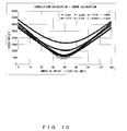
- FIG. 10 shows a result of performing the error calculation after performing the delay regulation in the 1/128 clock unit using a correlation value.
- FIG. 10 the horizontal axis shows the amount of delay in the 1/128 clock unit, and the vertical axis shows an error result.
- FIG. 10 shows substantially the same value as the optimum amount of delay although trial processes are repeated many times, and it proves that this method can set a reliable amount of delay.
- a distortion compensation coefficient can also be correctly updated.
- the process of delay regulation can be terminated by the delay regulation in the 1/128 clock unit by the correlation calculation of (2) above.
- FIG. 9 does not show an acute peak of the graph. Therefore, it seems that the peak cannot be easily detected, and correct delay can be obtained by further performing error calculation.
- FIG. 11 shows the entire configuration of the apparatus according to the mode for embodying the present invention.
- FIG. 11 the component also shown in FIG. 1 is assigned the same reference numeral, and the description is omitted here.
- a control unit (CPU) 26 is added.
- the control unit 26 acquires a correlation value and an error result as a process result from the correlation calculating unit 18 and the error calculating unit 19, and adjusts the amount of delay of the clock unit delay unit 16, the tap coefficient for determination of the amount of delay of the delay filter 20, and the phase of the demodulator 21.
- the phase adjustment of the demodulator 21 is performed by adjusting the phase of the oscillation wave of the numerical control oscillator 25 for supplying a periodical wave to the demodulator 21.
- the contents of the control of the control unit 26 is first acquiring a correlation value from the correlation calculating unit 18, and setting the optimum clock timing using the clock unit delay unit 16. Then, it acquires the correlation value from the correlation calculating unit 18, sets the operation timing using the delay filter 20, and at this time performs the phase adjustment of the demodulator 21. Finally, it acquires an error result from the error calculating unit 19, and sets the delay value as the optimum value using a delay filter.
- FIG. 12 is a flowchart of the process performed by the control unit shown in FIG. 11 .
- step S10 When the delay regulation is started, the correlation calculation is started in step S10.
- the correlation calculation in this case is performed in a clock unit.
- step S11 an amount of clock delay is changed.
- step S12 a correlation value after the change of the amount of clock delay is acquired.
- step S13 it is determined whether or not the amount of clock device has been changed at a specified number of times and a correlation value has been acquired. If the specified number of times has not been reached, control is returned to step S11, and the process is repeated the number of times. If it is determined in step S13 that the specified number of times has been reached, the maximum correlation value is calculated in step S14, and the amount of clock delay is set in step S15. In step S16, the correlation calculation is started.
- step S17 a filter coefficient (tap coefficient) is changed, and a correlation value is changed in step S18.
- step S19 it is determined whether or not a specified number of times has been reached. If not, control is returned to step S17, and the process is repeated. If it is determined in step S19 that the specified number of times has been reached, then control is passed to step S20, the maximum correlation value is calculated, and a tap coefficient is set in step S21.
- step S22 error calculation is started. The calculation is performed in a tap unit (for example, in the 1/128 clock unit).
- step S23 phase adjustment is performed.
- step S24 a filter coefficient is changed.
- step S25 an error value is acquired.
- step S26 it is determined whether or not the specified number of times has been reached. If not, the process is repeated. If it is determined in step S26 that the specified number of times has been reached, the minimum error value is calculated in step S27, and a tap coefficient is set in step S28, thereby terminating the process.
Landscapes
- Physics & Mathematics (AREA)
- Nonlinear Science (AREA)
- Engineering & Computer Science (AREA)
- Power Engineering (AREA)
- Amplifiers (AREA)
- Digital Transmission Methods That Use Modulated Carrier Waves (AREA)
- Transmitters (AREA)
Abstract
Description
- The present invention relates to a delay regulating device for a reference signal and a feedback signal in an adaptive predistorter (APD) type distortion compensation device.
- When distortion compensation is performed in the APD system, delay regulation is required to control timing between a reference signal (Ref signal) and a feedback signal (FB signal).
-
FIG. 1 is a block diagram of a transmission board to which the distortion compensation in the APD system is applied. - The reference signal (Ref signal) is a baseband signal of a transmission signal. The reference signal is input to a
multiplier 10, multiplied by a distortion compensation coefficient from a distortioncompensation control unit 15, and input to a D/A converter 11. When the D/A converter converts a digital signal into an analog signal, amodulator 12 modulates the signal, and apower amplifier 12 amplifies and transmits the signal. The modulator receives a radio frequency for up-conversion from alocal oscillator 14. - A reference signal is input to the distortion
compensation control unit 15. The reference signal input to the distortioncompensation control unit 15 is used to index a distortion compensation table. Furthermore, the reference signal is input to a clockunit delay unit 16. The reference signal is delayed by the clockunit delay unit 16 in a clock unit, and input to anadder 17 and acorrelation calculating unit 18. The clock of the clockunit delay unit 16 is controlled by thecorrelation calculating unit 18, and an amount of delay by the clockunit delay unit 16 is controlled by controlling the clock. - The signal output from the
power amplifier 12 is input to amultiplier 23 as a feedback signal (FB signal). Themultiplier 23 multiplies the signal by a radio frequency from alocal oscillator 24 for down-conversion. The output of themultiplier 23 is input to an A/D converter 22, and converted from an analog signal into a digital signal. The feedback signal converted into a digital signal is demodulated by ademodulator 21, and input to adelay filter 20. Thedelay filter 20 is typically a FIR filter, and can change the amount of delay of a signal by changing a tap coefficient. The output of thedelay filter 20 is input to a negative terminal of theadder 17 and thecorrelation calculating unit 18. Thecorrelation calculating unit 18 controls the phase of an oscillated wave of anumerical control oscillator 25 for inputting a periodical wave to thedemodulator 21. Thecorrelation calculating unit 18 calculates a correlation value between the reference signal and the feedback signal, and controls the clockunit delay unit 16 and thenumerical control oscillator 25 such that the correlation value can be higher. - The
adder 17 obtains a difference between the reference signal input to theadder 17 and the feedback signal input to the negative terminal of theadder 17, and inputs the result to the distortioncompensation control unit 15 and anerror calculating unit 19. Theerror calculating unit 19 adjusts the amount of delay of thedelay filter 20 such that the output of theadder 17 can be lower. An error signal as output of theadder 17 is used for update of a distortion compensation coefficient of a distortion compensation table stored in the distortioncompensation control unit 15. - The conventional adjustment of a relative amount of delay between a feedback signal and a reference signal is performed in the following two steps.
- (1) adjusting in a clock unit by a correlation calculation between a reference signal and a feedback signal
- (2) adjusting in 1/128 clock unit by an error calculation between a reference signal and a feedback signal
- In step (1) above, a reference signal is delayed in a clock unit, and an amount of delay for the maximum correlation value between the reference signal and the feedback signal is calculated.
-
FIG. 2 shows the circuit for performing the correlation calculation. - In
FIG. 2 , the reference signal and the feedback signal are complex signals each of the signals includes an I signal and a Q signal. Assuming that the I signal of the reference signal is Ref_ich, the Q signal of the reference signal is Ref_qch, the I signal of the feedback signal is FB_ich, and the Q signal of the feedback signal is FB_qch, the calculation performed by the circuit shown inFIG. 2 is expressed by the following equations.

then
where * indicates a complex conjugate, and j indicates an imaginary number unit. A correlation result real part integrator and a correlation result imaginary part integrator perform multiplication on a plurality of calculation results of a real part and an imaginary part of an obtained correlation value, and perform a calculation of a sum of the equations above. -
FIG. 3 shows an example of a result of a correlation calculation. -
FIG. 3 shows an example of a result of calculation of a correlation value by assigning various amounts of delay to a reference signal in a clock unit. A correlation value shows peaks at various amounts of delay, and shows the maximum peak value when the relative delay between the reference signal and the feedback signal shows the minimum value. Therefore, by detecting the amount of delay indicating the maximum peak value of the correlation value, the timing between the reference signal and the feedback signal can be detected. - Before performing the process in step (2) above, the amount of delay in a clock unit obtained in step (1) above is set. The
correlation calculating unit 18 adjusts the phase of thedemodulator 21 on the basis of the set delay. Thecorrelation calculating unit 18 performs the phase adjustment of thedemodulator 21 by calculating a phase value as follows. - By the correlation calculation, a phase value indicating the shift of the phase by the relative delay between the feedback signal and the reference signal can be acquired.
- Assuming that


thereby

As a result, the phase value is obtained as follows.
- The phase adjustment is performed to eliminate the phase difference between the reference signal and the feedback signal when the error calculation is performed in the delay regulation in step (2) above.
- After performing the phase adjustment of the
demodulator 21, the delay of the feedback signal is changed using a digital filter (delay filter). A tap coefficient for delay in 1/128 clock unit is prepared for the delay filter. By changing the tap coefficient, the delay of the feedback signal changes, and the optimum delay value of the reference signal and the feedback signal is obtained when a tap coefficient of the filter number indicating the minimum error value is selected. -
FIGS. 4A and 4B explain a digital filter. - A digital filter is specifically a FIR filter. As shown by
FIG. 4A , the digital filter includes a plurality of serially connected delay units, each multiplier for multiplying the output of each delay unit by a tap coefficient A0 ~ An, and an adder for adding up the output of each multiplier and outputting a result. To generate a delay in 1/128 clock unit, 128 delay units are provided. The delay value of each delay is 128 clocks. -
FIG. 4B shows an example of a tap coefficient, and is a plot having a vertical axis indicating the value of each tap coefficient when there are 11 taps. Although there are various methods of setting a tap coefficient, an amount of delay depends on the setting of each tap coefficient. -
FIG. 5 shows an example of a circuit for performing an error calculation, andFIG. 6 shows an example of an error calculation result. - The contents of the calculation by the error calculation circuit shown in
FIG. 5 are expressed by the following equations.

- Then, an error value is calculated as follows.

- As a result, the real part and the imaginary part of the difference are expressed as follows.


- An absolute value of the error value is obtained.
- The name of each variable is the same as that in the description of the correlation calculation. The error result real part integrator and the error result imaginary part integrator obtain a sum of the real part and the imaginary part of the error value.
-
FIG. 6 shows an amount of delay of a feedback signal in 1/128 clock unit along a horizontal axis, and shows an error value along the vertical axis. The amount of delay indicating the minimum error value is the optimum amount of delay. - However, the conventional system of adjusting an amount of delay has the following problem.
- The phase adjustment of the demodulator at the preceding stage of the error calculation in step (2) above is performed using the optimum point of the clock obtained in step (1) above and an initial value delay filter (initial value (0) in 1/128 clock unit), but there is the possibility that the filter tap coefficient of the optimum delay point is different from the delay filter tap coefficient of the initial value. In this case, the phase adj ustment is performed with a shifted delay, a correct phase cannot be obtained, thereby failing in obtaining a correct tap coefficient.
-
FIG. 7 shows the phase adjustment result of the demodulator using a tap coefficient (delay value), andFIG. 8 shows variations of the delay regulation results of the error calculation. -
FIG. 7 shows along the horizontal axis the number of times of performing the phase adjusting process, and shows along the vertical axis a change in phase value. The graph shows the three cases of set values of 0, 128, and 64 of the amount of delay in 1/128 clock unit. As shown by the graph, unless the tap coefficient of the delay filter is appropriate, the phase value is not close to 0 although the phase adjusting process is repeated many times. -
FIG. 8 shows the case in which a delay regulation is performed using a delay filter on the basis of a result of the error calculation.FIG. 8 shows a result of repeating the trial delay regulation several times, and the graphs using different marks refer to different trials. As shown inFIG. 8 , each time trial delay regulation is performed, a different amount of delay brings about the minimum error result, and the optimum reliable amount of delay cannot be obtained only by the delay regulation using an error result. - The conventional distortion compensation device can be the
patent document 1. Thepatent document 1 discloses a technique of not updating a distortion compensation table when a phase value is abnormal. - Patent Document 1: International Patent Application Publication No.
WO 03/103166 - The present invention aims at providing a delay regulating device capable of setting the timing of a reference signal and a feedback signal as a reliable and optimum value, and updating a correct distortion compensation coefficient.
- The delay regulating device according to the present invention is used in a distortion compensation device for calculating an error signal between a first signal and a second signal and updating a distortion compensation coefficient from the error signal, and adjusts an amount of delay of the first signal and the second signal. The delay regulating device includes: a correlation value calculation device calculating a correlation value between the first signal and the second signal; an error signal calculation device calculating an error signal between the first signal and the second signal; a first delay device adjusting a relative amount of delay between the first signal and the second signal; a second delay device adjusting the relative amount of delay between the first signal and the second signal in a unit smaller than the first delay device; and a control device first setting using the first delay device the relative amount of delay such that the correlation value is maximum, second adjusting using the second delay device the relative amount of delay such that the correlation value is maximum, and third readjusting using the second delay device the relative amount of delay such that the error signal is minimum.
-
-
FIG. 1 is a block diagram of a transmission board using distortion compensation in an APD system; -
FIG. 2 shows the circuit for performing correlation calculation; -
FIG. 3 shows an example of a correlation calculation result; -
FIGS. 4A and 4B explain a digital filter; -
FIG. 5 shows a circuit for performing error calculation; -
FIG. 6 shows an example of an error calculation result; -
FIG. 7 shows a phase adjustment result of a demodulator using a tap coefficient (delay value); -
FIG. 8 shows variations of delay regulation results in the error calculation; -
FIG. 9 shows the state of the amount of delay and the correlation value in 1/128 clock unit; -
FIG. 10 shows a result of performing error calculation after performing delay regulation in 1/128 clock unit using a correlation value; -
FIG. 11 shows the entire configuration of the apparatus according to the mode for embodying the present invention; and -
FIG. 12 is a flowchart of the process of the control unit shown inFIG. 11 . - According to this mode for embodying the present invention, the delay regulation is performed in the following procedure to solve the above-mentioned problem.
- (1) delay regulation in a clock unit by correlation calculation
- (2) filter tap delay regulation in 1/128 clock unit by correlation calculation
- (3) filter tap delay regulation in 1/128 clock unit by error calculation
- The delay regulation in (1) above is not limited to one clock unit. The delay regulation in (2) and (3) is also not limited to the 1/128 clock unit, but can be any unit smaller than the delay regulation unit of (1) above.
- By performing the above-mentioned procedure, the correlation calculation of (2) above requires no phase adj ustment, thereby performing the filter tap delay regulation without a large shift.
-
FIG. 9 shows the state of the amount of delay and correlation value in the 1/128 clock unit. - The horizontal axis shows the amount of delay in the 1/128 clock unit, and the vertical axis shows the correlation value. As clearly shown in
FIG. 9 , a substantially optimum amount of delay can be obtained using a correlation value in the 1/128 clock unit. - If the error calculation is performed by the tap coefficient of the delay filter as a result of the phase adjustment using the result of the optimum amount of delay, the calculation can be performed with a correct phase, and a correct filter tap coefficient can be obtained.
-
FIG. 10 shows a result of performing the error calculation after performing the delay regulation in the 1/128 clock unit using a correlation value. - In
FIG. 10 , the horizontal axis shows the amount of delay in the 1/128 clock unit, and the vertical axis shows an error result. UnlikeFIG. 8 ,FIG. 10 shows substantially the same value as the optimum amount of delay although trial processes are repeated many times, and it proves that this method can set a reliable amount of delay. By correctly setting the amount of delay, a distortion compensation coefficient can also be correctly updated. The process of delay regulation can be terminated by the delay regulation in the 1/128 clock unit by the correlation calculation of (2) above. However,FIG. 9 does not show an acute peak of the graph. Therefore, it seems that the peak cannot be easily detected, and correct delay can be obtained by further performing error calculation. -
FIG. 11 shows the entire configuration of the apparatus according to the mode for embodying the present invention. - In
FIG. 11 , the component also shown inFIG. 1 is assigned the same reference numeral, and the description is omitted here. - In
FIG. 11 , a control unit (CPU) 26 is added. Thecontrol unit 26 acquires a correlation value and an error result as a process result from thecorrelation calculating unit 18 and theerror calculating unit 19, and adjusts the amount of delay of the clockunit delay unit 16, the tap coefficient for determination of the amount of delay of thedelay filter 20, and the phase of thedemodulator 21. The phase adjustment of thedemodulator 21 is performed by adjusting the phase of the oscillation wave of thenumerical control oscillator 25 for supplying a periodical wave to thedemodulator 21. - The contents of the control of the
control unit 26 is first acquiring a correlation value from thecorrelation calculating unit 18, and setting the optimum clock timing using the clockunit delay unit 16. Then, it acquires the correlation value from thecorrelation calculating unit 18, sets the operation timing using thedelay filter 20, and at this time performs the phase adjustment of thedemodulator 21. Finally, it acquires an error result from theerror calculating unit 19, and sets the delay value as the optimum value using a delay filter. -
FIG. 12 is a flowchart of the process performed by the control unit shown inFIG. 11 . - When the delay regulation is started, the correlation calculation is started in step S10. The correlation calculation in this case is performed in a clock unit. In step S11, an amount of clock delay is changed. In step S12, a correlation value after the change of the amount of clock delay is acquired. In step S13, it is determined whether or not the amount of clock device has been changed at a specified number of times and a correlation value has been acquired. If the specified number of times has not been reached, control is returned to step S11, and the process is repeated the number of times. If it is determined in step S13 that the specified number of times has been reached, the maximum correlation value is calculated in step S14, and the amount of clock delay is set in step S15. In step S16, the correlation calculation is started. The correlation calculation is performed in a tap unit, that is, in the example above, in the 1/128 clock unit. In step S17, a filter coefficient (tap coefficient) is changed, and a correlation value is changed in step S18. In step S19, it is determined whether or not a specified number of times has been reached. If not, control is returned to step S17, and the process is repeated. If it is determined in step S19 that the specified number of times has been reached, then control is passed to step S20, the maximum correlation value is calculated, and a tap coefficient is set in step S21.
- In step S22, error calculation is started. The calculation is performed in a tap unit (for example, in the 1/128 clock unit). In step S23, phase adjustment is performed. In step S24, a filter coefficient is changed. In step S25, an error value is acquired. In step S26, it is determined whether or not the specified number of times has been reached. If not, the process is repeated. If it is determined in step S26 that the specified number of times has been reached, the minimum error value is calculated in step S27, and a tap coefficient is set in step S28, thereby terminating the process.
Claims (9)
- A delay regulating device which is used in a distortion compensation device for calculating an error signal between a first signal and a second signal and updating a distortion compensation coefficient from the error signal, and adjusts an amount of delay of the first signal and the second signal, comprising:a correlation value calculation means for calculating a correlation value between the first signal and the second signal;an error signal calculation means for calculating an error signal between the first signal and the second signal;a first delay means for adjusting a relative amount of delay between the first signal and the second signal;a second delay means for adjusting the relative amount of delay between the first signal and the second signal in a unit smaller than the first delay means; andfirst setting using the first delay means the relative amount of delay such that the correlation value is maximum, second adjusting using the second delay means the relative amount of delay such that the correlation value is maximum, and third readjusting using the second delay means the relative amount of delay such that the error signal is minimum.
- The device according to claim 1, wherein
the first delay means adjusts only an amount of delay of the first signal, and the second delay means adjusts only an amount of delay of the second signal. - The device according to claim 2, wherein
the first signal is a reference signal from a baseband signal. - The device according to claim 2, wherein
the second signal is a feedback signal obtained by demodulating a transmission signal. - The device according to claim 1, wherein
the first delay means adjusts an amount of delay in a clock unit. - The device according to claim 1, wherein
the second delay means is a digital filter. - The device according to claim 1, wherein
the second delay means adjusts an amount of delay in 1/128 clock unit. - The device according to claim 1, wherein
the control means sets optimum values of relative phases of the first and second signals after a second adjustment and before a third readjustment. - A delay regulating method which is used in a distortion compensation device for calculating an error signal between a first signal and a second signal and updating a distortion compensation coefficient from the error signal, and adjusts an amount of delay of the first signal and the second signal, comprising:providing a first delay means adjusting a relative amount of delay between the first signal and the second signal;providing a second delay means adjusting the relative amount of delay between the first signal and the second signal in a unit smaller than the first delay means;calculating a correlation value of the first signal and the second signal;calculating a error signal of the first signal and the second signal; andfirst setting using the first delay means the relative amount of delay such that the correlation value is maximum, second adjusting using the second delay means the relative amount of delay such that the correlation value is maximum, and third readjusting using the second delay means the relative amount of delay such that the error signal is minimum.
Applications Claiming Priority (1)
| Application Number | Priority Date | Filing Date | Title |
|---|---|---|---|
| PCT/JP2005/013974 WO2007013177A1 (en) | 2005-07-29 | 2005-07-29 | Delay regulating device |
Publications (4)
| Publication Number | Publication Date |
|---|---|
| EP1914884A1 true EP1914884A1 (en) | 2008-04-23 |
| EP1914884A4 EP1914884A4 (en) | 2008-10-29 |
| EP1914884B1 EP1914884B1 (en) | 2016-06-22 |
| EP1914884B8 EP1914884B8 (en) | 2016-09-21 |
Family
ID=37683085
Family Applications (1)
| Application Number | Title | Priority Date | Filing Date |
|---|---|---|---|
| EP05767437.6A Expired - Lifetime EP1914884B8 (en) | 2005-07-29 | 2005-07-29 | Delay regulating device |
Country Status (6)
| Country | Link |
|---|---|
| US (1) | US7466764B2 (en) |
| EP (1) | EP1914884B8 (en) |
| JP (1) | JP4664364B2 (en) |
| KR (1) | KR100959228B1 (en) |
| CN (1) | CN101228690B (en) |
| WO (1) | WO2007013177A1 (en) |
Cited By (2)
| Publication number | Priority date | Publication date | Assignee | Title |
|---|---|---|---|---|
| EP2290892A3 (en) * | 2009-08-12 | 2014-07-09 | Fujitsu Limited | Wireless apparatus and signal processing method |
| US10263569B2 (en) | 2012-07-23 | 2019-04-16 | Dali Systems Co. Ltd. | Method and system for aligning signals widely spaced in frequency for wideband digital predistortion in wireless communication systems |
Families Citing this family (16)
| Publication number | Priority date | Publication date | Assignee | Title |
|---|---|---|---|---|
| WO2009011071A1 (en) * | 2007-07-19 | 2009-01-22 | Fujitsu Limited | Amplifier device with nonlinear-distortion compensation |
| US8869891B2 (en) | 2007-11-19 | 2014-10-28 | Shell Oil Company | Systems and methods for producing oil and/or gas |
| US9057257B2 (en) | 2007-11-19 | 2015-06-16 | Shell Oil Company | Producing oil and/or gas with emulsion comprising miscible solvent |
| JP2009232425A (en) * | 2008-03-25 | 2009-10-08 | Toshiba Corp | Transmitter |
| RU2494239C2 (en) | 2008-04-16 | 2013-09-27 | Шелл Интернэшнл Рисерч Маатсхаппий Б.В. | Oil and/or gas extraction system and method |
| JP5251565B2 (en) * | 2009-02-05 | 2013-07-31 | 富士通株式会社 | Predistorter and delay adjustment method thereof |
| US8774314B2 (en) * | 2009-06-23 | 2014-07-08 | Qualcomm Incorporated | Transmitter architectures |
| EP2436114B1 (en) * | 2010-02-20 | 2019-07-10 | Huawei Technologies Co., Ltd. | Filter device and method for providing a filter device |
| CN102281044B (en) * | 2010-06-12 | 2016-07-20 | 澜起科技(上海)有限公司 | Blind adaptive filtering device and the application thereof of arrowband interference can be eliminated |
| JP5497552B2 (en) * | 2010-06-28 | 2014-05-21 | 京セラ株式会社 | Communication apparatus and distortion correction method |
| CN103257309B (en) * | 2012-02-17 | 2015-10-07 | 安凯(广州)微电子技术有限公司 | Ddr series pcb plate timing compensation method, system and terminal |
| JP6059003B2 (en) | 2012-12-26 | 2017-01-11 | パナソニック株式会社 | Distortion compensation apparatus and distortion compensation method |
| US9522738B2 (en) | 2015-04-23 | 2016-12-20 | Goodrich Corporation | Soft cover release mechanism for evacuation slides |
| CN105978843B (en) * | 2016-05-13 | 2019-02-12 | 京信通信系统(中国)有限公司 | Digital pre-distortion loop time delay method of adjustment and device |
| US10454509B2 (en) | 2018-03-13 | 2019-10-22 | Qualcomm Incorporated | Communication circuit including a transmitter |
| CN111107025B (en) * | 2018-10-26 | 2024-11-22 | 上海晟矽微电子股份有限公司 | Adaptive Equalizer in GFSK Receiver |
Family Cites Families (18)
| Publication number | Priority date | Publication date | Assignee | Title |
|---|---|---|---|---|
| FR2651339B1 (en) * | 1989-08-30 | 1991-10-04 | Alsthom Gec | DEVICE FOR CONTROLLING A FEEDBACK SYSTEM AND APPLICATION TO AMPLIFIERS AND SERVOMECHANISMS. |
| JP3268135B2 (en) * | 1994-09-06 | 2002-03-25 | 株式会社日立国際電気 | transceiver |
| KR100426422B1 (en) * | 1997-04-02 | 2004-04-08 | 뱅 앤드 올루프센 파워하우스 에이/에스 | Pulse referenced control method and system for enhanced power amplification of a pulse modulated signal |
| JP4014343B2 (en) * | 1999-12-28 | 2007-11-28 | 富士通株式会社 | Distortion compensation device |
| FR2835120B1 (en) * | 2002-01-21 | 2006-10-20 | Evolium Sas | METHOD AND DEVICE FOR PREPARING SIGNALS TO BE COMPARED TO ESTABLISH PRE-DISTORTION ON THE INPUT OF AN AMPLIFIER |
| JP3874688B2 (en) * | 2002-03-29 | 2007-01-31 | 富士通株式会社 | Distortion compensation device |
| WO2003103165A1 (en) * | 2002-05-31 | 2003-12-11 | 富士通株式会社 | Distortion compensator |
| EP1511181B1 (en) | 2002-05-31 | 2009-12-09 | Fujitsu Limited | Distortion compensator |
| JP2004015660A (en) * | 2002-06-10 | 2004-01-15 | Mitsubishi Electric Corp | Distortion compensator |
| JP2004040564A (en) * | 2002-07-04 | 2004-02-05 | Fujitsu Ltd | Power amplifier distortion compensation method and apparatus |
| WO2004034574A1 (en) * | 2002-10-10 | 2004-04-22 | Fujitsu Limited | Distortion compensation amplification apparatus, amplification system, and radio base station |
| JP3732824B2 (en) * | 2002-11-12 | 2006-01-11 | 株式会社日立国際電気 | Communication device |
| EP1432194A1 (en) * | 2002-12-19 | 2004-06-23 | Nokia Corporation | Adaptive predistortion scheme with delay tracking |
| JP2004214811A (en) * | 2002-12-27 | 2004-07-29 | Mitsumi Electric Co Ltd | Current feedback circuit |
| US7372917B2 (en) * | 2004-08-25 | 2008-05-13 | Broadcom Corporation | Digital algorithm for on-line ACPR optimization in polar RF transmitters |
| US7522658B2 (en) * | 2003-09-30 | 2009-04-21 | Broadcom Corporation | Design method and implementation of optimal linear IIR equalizers for RF transceivers |
| JP4436448B2 (en) * | 2004-01-14 | 2010-03-24 | 株式会社日立国際電気 | Distortion compensation amplifier |
| EP1791310B1 (en) * | 2004-09-13 | 2011-07-13 | Mitsubishi Electric Corporation | Distortion compensating apparatus |
-
2005
- 2005-07-29 CN CN2005800512314A patent/CN101228690B/en not_active Expired - Fee Related
- 2005-07-29 WO PCT/JP2005/013974 patent/WO2007013177A1/en not_active Ceased
- 2005-07-29 JP JP2007526798A patent/JP4664364B2/en not_active Expired - Fee Related
- 2005-07-29 KR KR1020087002105A patent/KR100959228B1/en not_active Expired - Fee Related
- 2005-07-29 EP EP05767437.6A patent/EP1914884B8/en not_active Expired - Lifetime
-
2008
- 2008-01-08 US US11/970,653 patent/US7466764B2/en not_active Expired - Fee Related
Cited By (2)
| Publication number | Priority date | Publication date | Assignee | Title |
|---|---|---|---|---|
| EP2290892A3 (en) * | 2009-08-12 | 2014-07-09 | Fujitsu Limited | Wireless apparatus and signal processing method |
| US10263569B2 (en) | 2012-07-23 | 2019-04-16 | Dali Systems Co. Ltd. | Method and system for aligning signals widely spaced in frequency for wideband digital predistortion in wireless communication systems |
Also Published As
| Publication number | Publication date |
|---|---|
| KR100959228B1 (en) | 2010-05-19 |
| EP1914884B8 (en) | 2016-09-21 |
| CN101228690A (en) | 2008-07-23 |
| CN101228690B (en) | 2010-08-18 |
| EP1914884B1 (en) | 2016-06-22 |
| KR20080018964A (en) | 2008-02-28 |
| US7466764B2 (en) | 2008-12-16 |
| EP1914884A4 (en) | 2008-10-29 |
| JPWO2007013177A1 (en) | 2009-02-05 |
| WO2007013177A1 (en) | 2007-02-01 |
| JP4664364B2 (en) | 2011-04-06 |
| US20080130798A1 (en) | 2008-06-05 |
Similar Documents
| Publication | Publication Date | Title |
|---|---|---|
| US7466764B2 (en) | Delay regulating device | |
| JP3844352B2 (en) | Transmitter | |
| KR100864558B1 (en) | Distortion compensating apparatus and method | |
| JP3035345B2 (en) | Apparatus and method for reducing distortion in amplification | |
| CN100359801C (en) | Mixed distortion compensation method and mixed distortion compensation device | |
| JP5375683B2 (en) | Communication apparatus and power correction method | |
| KR100421145B1 (en) | Compensating method and circuit of non-linear distortion | |
| US20050111575A1 (en) | Amplifier linearization using non-linear predistortion | |
| EP2254241A2 (en) | Power series digital predistorter and control method therefor | |
| EP2290892A2 (en) | Wireless apparatus and signal processing method | |
| US7496152B2 (en) | Adaptive control apparatus | |
| EP1819039A1 (en) | Distortion compensating apparatus and method | |
| US20070274471A1 (en) | Distortion compensating apparatus and method | |
| US7881404B2 (en) | Distortion correction control apparatus and distortion correction control method | |
| EP1811655A1 (en) | A power amplifier distortion compensation apparatus and method thereof | |
| JP2007267345A (en) | Transmitter and carrier leak detection method | |
| EP1724956A1 (en) | Radio system and radio communication device | |
| EP2067252B1 (en) | Adaptive self-linearization | |
| KR20060024790A (en) | Communication system, wireless transceiver unit, integrated circuit and method for continuously compensating for phase deviation introduced into communication signal by automatic gain control adjustment | |
| EP1848108B1 (en) | Distortion compensating apparatus and method | |
| JP4127639B2 (en) | Nonlinear compensator | |
| JP6286908B2 (en) | Amplifying device and wireless communication device | |
| EP2290831A2 (en) | Transmission device and transmission method | |
| JP2008072522A (en) | Loopback delay correction device and loopback delay correction method | |
| US20190089407A1 (en) | Reception apparatus, transmission apparatus, and communication system |
Legal Events
| Date | Code | Title | Description |
|---|---|---|---|
| PUAI | Public reference made under article 153(3) epc to a published international application that has entered the european phase |
Free format text: ORIGINAL CODE: 0009012 |
|
| 17P | Request for examination filed |
Effective date: 20080225 |
|
| AK | Designated contracting states |
Kind code of ref document: A1 Designated state(s): DE FR GB |
|
| RBV | Designated contracting states (corrected) |
Designated state(s): DE FR GB |
|
| A4 | Supplementary search report drawn up and despatched |
Effective date: 20080926 |
|
| 17Q | First examination report despatched |
Effective date: 20090108 |
|
| DAX | Request for extension of the european patent (deleted) | ||
| GRAP | Despatch of communication of intention to grant a patent |
Free format text: ORIGINAL CODE: EPIDOSNIGR1 |
|
| INTG | Intention to grant announced |
Effective date: 20160115 |
|
| GRAS | Grant fee paid |
Free format text: ORIGINAL CODE: EPIDOSNIGR3 |
|
| GRAA | (expected) grant |
Free format text: ORIGINAL CODE: 0009210 |
|
| REG | Reference to a national code |
Ref country code: FR Ref legal event code: PLFP Year of fee payment: 12 |
|
| RIN1 | Information on inventor provided before grant (corrected) |
Inventor name: OHBA, TAKESHI Inventor name: SHAKO, HIDEHARU Inventor name: FUNYU, YASUHITO |
|
| AK | Designated contracting states |
Kind code of ref document: B1 Designated state(s): DE FR GB |
|
| REG | Reference to a national code |
Ref country code: GB Ref legal event code: FG4D |
|
| REG | Reference to a national code |
Ref country code: DE Ref legal event code: R096 Ref document number: 602005049570 Country of ref document: DE |
|
| RIN2 | Information on inventor provided after grant (corrected) |
Inventor name: SHAKO, HIDEHARU Inventor name: OHBA, TAKESHI Inventor name: FUNYU, YASUHITO |
|
| REG | Reference to a national code |
Ref country code: DE Ref legal event code: R097 Ref document number: 602005049570 Country of ref document: DE |
|
| PLBE | No opposition filed within time limit |
Free format text: ORIGINAL CODE: 0009261 |
|
| STAA | Information on the status of an ep patent application or granted ep patent |
Free format text: STATUS: NO OPPOSITION FILED WITHIN TIME LIMIT |
|
| 26N | No opposition filed |
Effective date: 20170323 |
|
| REG | Reference to a national code |
Ref country code: FR Ref legal event code: PLFP Year of fee payment: 13 |
|
| REG | Reference to a national code |
Ref country code: FR Ref legal event code: PLFP Year of fee payment: 14 |
|
| PGFP | Annual fee paid to national office [announced via postgrant information from national office to epo] |
Ref country code: FR Payment date: 20180612 Year of fee payment: 14 |
|
| PGFP | Annual fee paid to national office [announced via postgrant information from national office to epo] |
Ref country code: DE Payment date: 20180717 Year of fee payment: 14 |
|
| PGFP | Annual fee paid to national office [announced via postgrant information from national office to epo] |
Ref country code: GB Payment date: 20180725 Year of fee payment: 14 |
|
| REG | Reference to a national code |
Ref country code: DE Ref legal event code: R119 Ref document number: 602005049570 Country of ref document: DE |
|
| GBPC | Gb: european patent ceased through non-payment of renewal fee |
Effective date: 20190729 |
|
| PG25 | Lapsed in a contracting state [announced via postgrant information from national office to epo] |
Ref country code: GB Free format text: LAPSE BECAUSE OF NON-PAYMENT OF DUE FEES Effective date: 20190729 Ref country code: DE Free format text: LAPSE BECAUSE OF NON-PAYMENT OF DUE FEES Effective date: 20200201 |
|
| PG25 | Lapsed in a contracting state [announced via postgrant information from national office to epo] |
Ref country code: FR Free format text: LAPSE BECAUSE OF NON-PAYMENT OF DUE FEES Effective date: 20190731 |