EP1912465A2 - Steuerungssystem eines optischen Mehrkanalvermittlers - Google Patents
Steuerungssystem eines optischen Mehrkanalvermittlers Download PDFInfo
- Publication number
- EP1912465A2 EP1912465A2 EP07007869A EP07007869A EP1912465A2 EP 1912465 A2 EP1912465 A2 EP 1912465A2 EP 07007869 A EP07007869 A EP 07007869A EP 07007869 A EP07007869 A EP 07007869A EP 1912465 A2 EP1912465 A2 EP 1912465A2
- Authority
- EP
- European Patent Office
- Prior art keywords
- switching
- channel
- optical switch
- register
- value
- Prior art date
- Legal status (The legal status is an assumption and is not a legal conclusion. Google has not performed a legal analysis and makes no representation as to the accuracy of the status listed.)
- Withdrawn
Links
Images














Classifications
-
- H—ELECTRICITY
- H04—ELECTRIC COMMUNICATION TECHNIQUE
- H04Q—SELECTING
- H04Q11/00—Selecting arrangements for multiplex systems
- H04Q11/0001—Selecting arrangements for multiplex systems using optical switching
- H04Q11/0005—Switch and router aspects
-
- H—ELECTRICITY
- H04—ELECTRIC COMMUNICATION TECHNIQUE
- H04Q—SELECTING
- H04Q11/00—Selecting arrangements for multiplex systems
- H04Q11/0001—Selecting arrangements for multiplex systems using optical switching
- H04Q11/0005—Switch and router aspects
- H04Q2011/0007—Construction
- H04Q2011/0024—Construction using space switching
-
- H—ELECTRICITY
- H04—ELECTRIC COMMUNICATION TECHNIQUE
- H04Q—SELECTING
- H04Q11/00—Selecting arrangements for multiplex systems
- H04Q11/0001—Selecting arrangements for multiplex systems using optical switching
- H04Q11/0005—Switch and router aspects
- H04Q2011/0037—Operation
- H04Q2011/0039—Electrical control
-
- H—ELECTRICITY
- H04—ELECTRIC COMMUNICATION TECHNIQUE
- H04Q—SELECTING
- H04Q11/00—Selecting arrangements for multiplex systems
- H04Q11/0001—Selecting arrangements for multiplex systems using optical switching
- H04Q11/0005—Switch and router aspects
- H04Q2011/0037—Operation
- H04Q2011/0043—Fault tolerance
-
- H—ELECTRICITY
- H04—ELECTRIC COMMUNICATION TECHNIQUE
- H04Q—SELECTING
- H04Q11/00—Selecting arrangements for multiplex systems
- H04Q11/0001—Selecting arrangements for multiplex systems using optical switching
- H04Q11/0005—Switch and router aspects
- H04Q2011/0052—Interconnection of switches
- H04Q2011/0058—Crossbar; Matrix
Definitions
- the present invention contains subject matter related to Japanese Patent Application No. 2006-221252 filed in the Japan Patent Office on August 14, 2006, the entire contents of which being incorporated herein by reference.
- the present invention relates to a control system of a multichannel optical switch utilizing an electro-optical effect (EO effect), more particularly relates to a control system of a multichannel optical switch preventing heat generation of the optical switch devices due to a leakage current between electrodes of the optical switch devices and the ground or between wires.
- EO effect electro-optical effect
- Optical switches using devices having the Pockels effect, Kerr effect, or another EO effect have various merits compared with mechanical optical switches (MEMS) such as a faster operating speed and a longer life than mechanical switches and are promising for application to systems for switching large capacity optical circuits at a high speed (for example, optical routers etc.) (below, such optical switches having such an EO effect being referred to as "EO-SWs” or simply "optical switches”).
- MEMS mechanical optical switches
- An EO-SW is characterized by changing the deflection angle in accordance with the magnitude of the electric field given or its change (relating to electrode area or applied voltage).
- FIG. 1 is a perspective view of one known optical switch.
- 11 is a ground plate
- 12 is a prism-shaped optical switch device formed by PLZT (lanthanum-doped lead zirconium titanate)
- 13 is an electrode plate formed on the top surface of the optical switch device 12
- 14 is a power source applying a voltage V between the ground plate 11 and electrode plate 13.
- the input light 15 passes through the optical switch 12 as output light 16 without being refracted. After applying the voltage V, the input light 15 is refracted and becomes the output light 17.
- FIG. 2 is a block diagram of the configuration of a conventional control system of a two-channel optical switch.
- 211 to 214 are input side optical switch devices
- 215 to 219 are output side optical switch devices
- 220 is a ground plate
- 221 to 224 are power sources applying voltage to the respective input side optical switch devices 211 to 214
- 225 to 228 are power sources applying voltage to the respective output side optical switch devices 215 to 219
- 230 is a control unit controlling the output voltages of the power sources 221 to 228.
- the control signals are manually input to the control unit.
- the drive unit was comprised of a plurality of power sources controlled individually for each electrode of the optical switch devices.
- the optical switch devices 213, 214, 218, and 219 are supplied with the voltage V1-1, the optical signal input from the OptIN1 of the first channel is output to OptOUT1 whereby the path 1-1 is established, while if the optical switch devices 213, 214, 215, and 216 are supplied with the voltage V1-2, it is output to OptOUT2 whereby the path 1-2 is established.
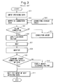
- FIG. 3 is a flowchart for explaining the operation of the conventional control system of the two-channel optical switch shown in FIG. 2.
- the control unit 230 when switching data is manually input from the outside to the control unit 230 at step 301, the control unit 230 refers to a connection memory table 303 to refer to the current state of path connection at step 302 and judges whether to allow connection at step 304. If the channel to be used for the input switching data is not yet in use, it allows connection, while if it is being used, it judges there is a connection error at step 305 and does not allow the connection.
- the system applies a desired voltage to predetermined electrodes at step 306, then waits for a certain time at step 307 and monitors the status at step 308.
- it compares the error and judges whether the error between the input data and connection data is within a certain range. If within a certain range, at step 310, it finely adjusts the electrode voltage, then, at step 311, waits for the next input of switching data.
- the judgment in the comparison of error at step 309 corrects for aging of the EO-SW, fluctuations in temperature, and other factors behind fluctuation so that the applied voltage becomes always optimal.
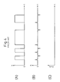
- FIG. 4 is a graph for explaining the operation of the conventional control system of the two-channel optical switch shown in FIG. 2.
- (A) is a graph showing the changes along with time in the example of voltage applied to one optical switch device
- (B) is a graph showing the leakage current generated by the applied voltage
- (C) is a graph showing the change in temperature produced by the applied voltage.
- leakage current as shown in (B) is generated by the rise and fall of the applied voltage, but the interval between generation of the leakage current is long, so almost no heat is generated as shown in (C).
- FIG. 5 is a view showing the state of current leaking from the electrodes of optical switch devices 51 to 54 to a ground plate 55.
- FIG. 6 is a view showing the leakage current generated between wires 605 to 608 connected to the electrodes of optical switch devices 601 to 604 and wires 613 to 616 connected to electrodes of optical switch devices 609 to 612.
- FIG. 7 is a graph showing the leakage current and the state of heat generation when a conventional control system of an optical switch continuously switches paths at a high speed.
- (A) if changing the voltage applied to the electrodes of the optical switch devices continuously at a high speed, as shown by (B), leakage current is continuously generated and, as a result, as shown in (C), the temperature of the optical switch devices rises along with the elapse of time.
- (B) if changing the voltage applied to the electrodes of the optical switch devices continuously at a high speed, as shown by (B), leakage current is continuously generated and, as a result, as shown in (C), the temperature of the optical switch devices rises along with the elapse of time.
- An object of the present invention in considering the problems of the above stated related art, is to provide a control system of an optical switch controlling the switching operation in a multichannel, highly integrated EO-SW so as to suppress the generation of leakage current and enable stable operation.
- a control system of optical switch devices of a multichannel optical switch using devices having an electro-optical effect the control system of a multichannel optical switch provided with a switching data input device for inputting switching data of the optical switch devices from a path switching instruction device, an elapsed time recording device for recording an elapsed time EL_T from which the switching data starts to be output from the path switching instruction device, a judgment data recording device for recording judgment data for judging whether switching of the optical switch devices is possible based on the switching data, an elapsed time judgment device for determining whether the elapsed time EL_T has exceeded a predetermined counted time threshold Am_T, a switching judgment processing device for judging switching based on an output of the elapsed time judgment device and an output of the judgment data recording device, and an electrode voltage application device, the electrode voltage application device applying voltage for switching the optical switch devices based on the switching data when the elapsed time judgment device has judged that
- the switching data input device is provided with a Vt1 register for recording a voltage Vt1 applied by a path connection of before switching of the optical switch devices and a Vt2 register for recording a voltage Vt2 applied by a path connection of after switching of the optical switches
- the judgment data recording device is provided with a Vts register for recording an absolute value Vts of a difference of the voltage Vt1 and voltage Vt2 and a Vtsm register for adding a value stored in the Vts register to a switching channel difference sum Vtsm to update the switching channel difference sum Vtsm
- the elapsed time recording device is an EL_T register for recording the elapsed time EL_T
- the switching judgment processing device is provided with a VtsmA register for storing a value VtsmA obtained by dividing the Vtsm value by the elapsed time EL_T when the elapsed time judgment device has judged
- the switching data input device and judgment data recording device are provided with an Sw register for recording the switching count Sw of the optical switch devices
- the elapsed time recording device is an EL_T register for recording the elapsed time EL_T
- the switching judgment processing device is provided with an SwA register for storing an SwA value obtained by dividing the switching count Sw by the elapsed time EL_T when the elapsed time judgment device has judged that the predetermined counted time threshold Am_T has been exceeded and a comparison device for comparing the SwA value with a predetermined electrode voltage application judgment threshold SwA_TH, the value of the Sw register and the value of the EL_T register are cleared to a predetermined initial value when the division is ended, and the electrode voltage application device applies voltage for switching the optical switch devices based on the switching data to switch the optical switch devices when the SwA value is smaller than the predetermined electrode voltage application judgment threshold SwA_TH and sends a switching failure notice
- the switching data input device is provided with a Vt1 register for recording a voltage Vt1 applied by a path connection of before switching of the optical switch devices and a Vt2 register for recording a voltage Vt2 applied by a path connection of after switching of the optical switches
- the judgment data recording device is provided with a Vts register for recording an absolute value Vts of a difference between the voltage Vt1 and the voltage Vt2 and a Vtsm register for adding a value stored in the Vts register to a switching channel difference sum Vtsm to update the switching channel difference sum Vtsm
- the elapsed time recording device is an EL_T register for recording the elapsed time EL_T
- the switching judgment processing device is provided with a.WvtsmA register for storing a channel switching heat generation calculated value (WvtsmA value) obtained by subtracting from a product of the switching channel difference sum Vtsm and a
- the switching data input device and judgment data recording device are provided with an Sw register for recording the switching count Sw of the optical switch devices
- the elapsed time recording device is an EL_T register for recording the elapsed time EL_T
- the switching judgment processing device is provided with a WswA register for storing a WswA value obtained by subtracting from a product of the switching count Sw and a coefficient Wsw for deriving the amount of heat generation envisioned from the switching count Sw the product of the elapsed time EL_T and a coefficient Wsw_loss for deriving the amount of natural heat generation envisioned from the elapsed time EL_T when the elapsed time judgment device has judged that the predetermined counted time threshold Am_T has been exceeded and a comparison device for comparing the WswA value with a predetermined WswA threshold WswA_TH, the value of the Sw register and the value of the
- the switching data input device is provided with an applied voltage register for recording a working channel applied voltage V 1 for the optical switch device of a working channel, a preceding channel applied voltage V 1 - for the optical switch device of the preceding channel adjoining the working channel, and a succeeding channel applied voltage V 1+ for the optical switch device of the succeeding channel adjoining the working channel
- the judgment data recording device is provided with a register for storing a preceding adjoining channel voltage difference Vtc1 between the working channel applied voltage V 1 and the preceding channel applied voltage V 1- and a succeeding adjoining channel voltage difference Vtc2 between the applied voltage V 1 and the applied voltage V 1+
- a comparison device for comparing the absolute value of the preceding adjoining channel voltage difference Vtc1 and the absolute value of the succeeding adjoining channel voltage difference Vtc2
- a conversion device for converting the greater adjoining channel voltage difference among the absolute value of the preceding adjoining channel voltage difference Vtc1 and the
- the switching data input device is provided with an applied voltage register for recording a working channel applied voltage V 1 for the optical switch device of a working channel, a preceding channel applied voltage V 1 - for the optical switch device of the preceding channel adjoining the working channel, and a succeeding channel applied voltage V 1+ for the optical switch device of the succeeding channel adjoining the working channel
- the judgment data recording device is provided with a register for storing a preceding adjoining channel voltage difference Vtc1 between the working channel applied voltage V 1 and the preceding channel applied voltage V 1 - and a succeeding adjoining channel voltage difference Vtc2 between the applied voltage V 1 and the applied voltage V 1+
- a first comparison device for comparing the absolute value of the preceding adjoining channel voltage difference Vtc1 and an adjoining channel difference judgment threshold Vtc_TH
- a second comparison device for comparing the absolute value of the succeeding adjoining channel voltage difference Vtc2 and the adjoining channel difference judgment threshold V
- the switching data input device is provided with an applied voltage register for recording a working channel applied voltage V 1 for the optical switch device of a working channel, a preceding channel applied voltage V 1 - for the optical switch device of the preceding channel adjoining the working channel, and a succeeding channel applied voltage V 1+ for the optical switch device of the succeeding channel adjoining the working channel
- the judgment data recording device is provided with a register for storing a preceding adjoining channel voltage difference Vtc1 between the working channel applied voltage V 1 and the preceding channel applied voltage V 1 - and a succeeding adjoining channel voltage difference Vtc2 between the applied voltage V 1 and the applied voltage V 1+
- a comparison device for comparing the absolute value of the preceding adjoining channel voltage difference Vtc1 and the absolute value of the succeeding adjoining channel voltage difference Vtc2
- a conversion device for converting the greater adjoining channel voltage difference among the absolute value of the preceding adjoining channel voltage difference Vtc1 and
- the switching data input device is provided with an applied voltage register for recording a working channel applied voltage V 1 for the optical switch device of a working channel, a preceding channel applied voltage V 1- for the optical switch device of the preceding channel adjoining the working channel, and a succeeding channel applied voltage V 1+ for the optical switch device of the succeeding channel adjoining the working channel
- the judgment data recording device is provided with a register for storing a preceding adjoining channel voltage difference Vtc1 between the working channel applied voltage V 1 and the preceding channel applied voltage V 1 - and a succeeding adjoining channel voltage difference Vtc2 between the applied voltage V 1 and the applied voltage V 1+
- a first comparison device for comparing the absolute value of the preceding adjoining channel voltage difference Vtc1 and an adjoining channel difference judgment threshold Vtc_TH
- a second comparison device for comparing the absolute value of the succeeding adjoining channel voltage difference Vtc2 and the adjoining channel difference judgment threshold Vtc_
- the present invention by rejecting continuous high speed requests for switching by certain criteria, it is possible to keep down the frequency of occurrence of leakage current, so it is possible to keep down a rise in temperature of the optical switches and stably control and operate EO-SWs.
- FIG. 8 is a block diagram showing the schematic configuration of a control system of a multichannel optical switch according to an embodiment of the present invention.
- 801 is a path switching instruction device and 802 is a control system of a multichannel optical switch (EO-SW control system).
- the EO-SW control system 802 is provided with a control unit 803, a drive unit 804, a monitor unit 805, optical switch devices 811 and 812 of a channel 1 of the input side, optical switch devices 821 and 822 of a channel 2, optical switch devices 8N1 and 8N2 of ... a channel N, optical switch devices 813 and 814 of the output side, optical switch devices 823 and 825 of the channel 2, and optical switch devices 8N3 and 8N4 of the ... channel N.
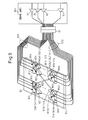
- FIG. 9 is an enlarged view of a part of FIG. 8.
- the optical switch devices 811 to 8N4 are arranged between a ground plate 81 and an electrode plate 82.
- the wires 910 are connected from the drive devices 91, 92, 93, ... 9x inside the drive unit 804 through a wire bundling unit 91 to the electrodes of the optical switch devices 811 to 8N3.
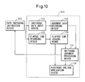
- FIG. 10 is a block diagram of the configuration of the control unit 803 inside the EO-SW control system 802 shown in FIG. 8.
- the control unit 803 is a control unit of the individual optical switch devices of a multichannel optical switch using devices having an electro-optical effect.
- the control unit 803 is provided with a switching data input device 101 for inputting switching data of the optical switch devices from the path switching instruction device 801, an elapsed time recording device 102 for recording the elapsed time EL_T from the time when the switching data started to be output from the path switching instruction device 801, a judgment data recording device 103 for recording judgment data for judging whether the optical switch devices can be switched based on the switching data, an elapsed time judgment device 104 for judging whether the elapsed time EL_T has exceeded a predetermined counted time threshold Am_T, a switching judgment processing device 105 for judging switching based on the output of the elapsed time judgment device and the output of the judgment data recording device, and an electrode voltage application device 106.
- a switching data input device 101 for inputting switching data of the optical switch devices from the path switching instruction device 801
- an elapsed time recording device 102 for recording the elapsed time EL_T from the time when the switching data started to be output from the path switching
- the electrode voltage application device 106 applies voltage for switching the optical switch devices based on the switching data.
- the electrode voltage application device 106 applies voltage to the optical switch devices to switch the optical switch devices based on the switching data.
- the switching judgment processing device 105 judges that the predetermined switching conditions have not been met, the electrode voltage application device 106 does not apply voltage for switching the optical switch devices to the switch devices and the switching judgment processing device 105 sends a switching failure notice to the path switching instruction device 801.
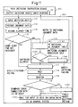
- FIG. 11 is a flowchart for explaining the operation of the control unit 803 shown in FIG. 10.
- the path switching instruction device 801 is provided with a switching data output port 111 and a response input port 123.
- the control unit 803 inputs the switching data of the switching data output port 111 into the switching data input device 101.
- it records judgment data obtained based on the switching data in the judgment data recording device 103.
- it records the elapsed time EL_T from the time when the switching data began to be output from the path switching instruction device 801 in the elapsed time recording device 102.
- the elapsed time judgment device 104 judges whether the elapsed time EL_T has exceeded the predetermined counted time threshold Am_T.
- the switching judgment processing device 105 performs the switching judgment processing.
- the switching judgment processing device 105 accesses the switching judgment table 1162 inside the judgment data recording device 103 to refer to the switching judgment data and, at step 1163, judges whether switching is allowed based on this switching judgment data.
- it sends a switching failure notice to the response input port 123 of the path switching instruction device 801.
- the control unit supplies voltage to the electrodes of the correspondingly optical switch devices. After this, in a similar manner, at step 118, it waits for a certain time, then, at step 119, performs monitoring. At 1191, it compares the error to determine if the error between the connection data and the actually connected electrodes is within a certain range. If this error is within a certain range, at step 1192, it waits for the input of the next switching data. If outside the certain range, at step 1193, it finely adjusts the voltage applied to the corresponding electrodes, then at step 121 waits for the input of the next switching data.
- control unit performs correction processing to correct for aging of the EO-SW, fluctuations in temperature, and other factors causing fluctuation so that the applied voltage becomes constantly optimal.
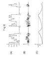
- FIG. 12 is a graph showing the relationship among the applied voltage, generation of leakage current, and heat generation of optical switch devices due to the processing shown in FIG. 11.
- the control unit stops application of voltage to the electrodes between the time t1 to t2 and between t3 to t4, whereby, as shown by (B), no leakage current is generated any longer during those intervals and, consequently, as shown by (C), the temperature of the optical switch devices no longer exceeds the threshold TH.
- FIG. 13 is a block diagram showing the configuration of a control system of a multichannel optical switch according to Example 1 of the present invention.
- the switching data input device 101 of FIG. 10 is realized by a switching data input device 1011 and is provided with a pre-connection path connection voltage register (Vt1 register) 131 for recording a voltage Vt1 applied by the path connection of before switching of the optical switch devices and a post-connection path connection voltage register (Vt2 register) 132 for recording a voltage V2 applied by the path connection of after switching of the optical switch devices.
- Vt1 register pre-connection path connection voltage register
- Vt2 register post-connection path connection voltage register
- the judgment data recording device 103 of FIG. 10 is realized in Example 1 by a judgment data recording device 1031 and is provided with a connection difference temporary recording register (Vts register) 133 for recording an absolute value Vts of the difference between the voltage Vt1 and voltage Vt2 and a connection voltage storage register (Vtsm register) 134 for adding the value stored in the Vts register to the switching channel difference sum Vtsm to update the switching channel difference sum Vtsm.
- Vts register connection difference temporary recording register
- Vtsm register connection voltage storage register
- the elapsed time recording device 104 of FIG. 10 is realized in Example 1 by an elapsed time count up register (EL_T register) 135 for recording the elapsed time EL_T.
- the switching judgment processing device 105 of FIG. 10 is realized by a switching judgment processing device 1051 and is provided with a unit time connection voltage difference storage register (VtsmA register) 137 for storing a value VtsmA obtained by dividing the Vtsm value by the elapsed time EL_T when the elapsed time judgment device 136 judges that a predetermined counted time threshold Am_T has been exceeded and a comparison device 138 for comparing the VtsmA value and a predetermined electrode voltage application judgment threshold Vtsma_TH.
- the values of the EL_T register 135 and Vtsm register 134 are cleared to for example 0 to be initialized when the above division for storing the value VtsmA in the VtsmA register 137 ends.
- the electrode voltage application device 106 of FIG. 10 is realized in this example by an electrode voltage application device 139.
- an electrode voltage application device 139 When the VtsmA value inside the VtsmA register 137 is smaller than a predetermined electrode voltage application judgment threshold VtsmA_TH, it applies voltage for switching of the optical switch devices based on the switching data to the optical switch devices, while when the VtsmA value inside the VtsmA register 137 is the predetermined electrode voltage application judgment threshold VtsmA_TH or more, it sends a switching failure notice to the path switching instruction device.
- FIG. 14 is a flowchart for explaining the operation of the control system of a multichannel optical switch according to Example 1 shown in FIG. 13.
- the system inputs switching data from the switching data output port 111 into the switching data input device 1011, while at step 142, it records a pre-switching path connection voltage VT1 in the Vt1 register 131 and records a post-switching path connection voltage Vt2 in the Vt2 register 132 based on the switching data.
- the initial value of Vtsm is for example 0.
- it records the elapsed time EL_T from the time after the switching data starts to be output from the path switching instruction device 801 in the elapsed time recording device (EI_T register) 102.
- the system uses the elapsed time judgment device 136 to judge whether the elapsed time EL_T has exceeded the predetermined counted time threshold Am_T.
- the elapsed time EL_T has exceeded the counted time threshold Am_T
- it divides the Vtsm by EI_T and records the resultant VtsmA in the VtsmA register 137.
- it for example clears the values of the ET_T register 145 and Vtsm register 144 to 0 to initialize them.
- the system uses the comparison device 138 to compare the VtsmA value with the connection voltage difference threshold VtsmA_TH. If VtsmA ⁇ VtsmA_TH, then at step 1491, the system supplies voltage to the electrodes of the corresponding optical switch devices. If VtsmA ⁇ VtsmA_TH, then at step 1492, the system stops the application of electrode voltage and, at step 1493, notifies switching failure to the response input port 123 of the path switching instruction device 801.
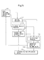
- FIG. 15 is a block diagram of the configuration of a control system of a multichannel optical switch according to Example 2 of the present invention.
- the switching data input device 101 of FIG. 10 is realized in Example 2 by an Sw register 151 for recording the switching count Sw of the optical switch devices.
- the elapsed time recording device 102 of FIG. 10 is realized in Example 2 by an elapsed time count up register (EL_T register) 152 for recording the elapsed time EL_T in the same way as Example 1, while the judgment data recording device 103 of FIG. 10 is realized in Example 2 by an EI_T ⁇ Am_TH comparison device 153 in the same way as Example 1.
- Example 10 is realized in Example 2 by a switching judgment processing device 1052 and is provided with a unit time switching time storage register (SwA register) 154 for storing the SwA value obtained by dividing the switching count Sw by the elapsed time EL_T when the comparison device 153 judges the predetermined counted time threshold Am_T is exceeded and a comparison device 155 for comparing the SwA value and a predetermined switching channel count threshold SwA_TH.
- the electrode voltage application device 106 of FIG. 10 is realized in Example 2 by an electrode voltage application device 156.
- the values of the Sw register 151 and the EL_T register 152 are for example cleared to 0 to be initialized when the division at the SwA register 154 ends.
- the electrode voltage application device 156 applies voltage for switching the optical switch devices based on the switching data to the optical switch devices when the SwA value is smaller than the predetermined switching channel count threshold SwA_TH and sends a switching failure notice to the path switching instruction device when the SwA value is the predetermined switching channel count threshold SwA_TH or more.
- FIG. 16 is a flowchart for explaining the operation of the control system of a multichannel optical switch according to Example 2 shown in FIG. 15.
- the system inputs switching data from the switching data output port 111 into the Sw register 151.
- the switching data is only data for notifying the fact that the optical switch devices have been switched.
- the system increments the switching count Sw to update it. That is, after the switching data of a path is input for a predetermined channel, the system increments the value of the Sw register 151 by one. For example, in a state where a path is laid between the input channel 1 and output channel 3, if switching from the input channel 1 to the output party 2, the system increments the value of the Sw register 151 by exactly one.
- the system records the elapsed time EL_T from when the switching data starts to be output from the path switching instruction device 801 in the elapsed time count up register (EI_T register) 152.
- EI_T register elapsed time count up register
- the system uses the judgment device 153 to judge whether the elapsed time EL_T has exceeded the predetermined counted time threshold Am_T.
- the system divides the switching count Sw by the EI_T and records the result SwA in the unit time switching count storage register (SwA register) 154.
- the system clears the values of the ET_T register 152 and the Sw register 151 to 0 to initialize them.
- step 167 the system compares the SwA value with the connection voltage difference threshold SwA_TH. If SwA ⁇ SwA_TH, then at step 168, it supplies voltage to the electrodes of the corresponding optical switch devices. If SwA ⁇ SwA_TH, then at step 169, the system stops the application of the electrode voltage, then at step 1691 it notifies switching failure to the response input port 123 of the path switching instruction device 801.
- FIG. 17 is a block diagram showing the configuration of a control system of a multichannel optical switch according to Example 3 of the present invention.
- the Vt1 register 131 and the Vt2 register 132 inside the switching data input device 1011 in Example 1 shown in FIG. 13 are the same as a Vt1 register 171 and a Vt2 register 172 in a switching data input device 1013 in Example 3.
- the Vts register 133 and the Vtsm register 134 in the judgment data recording device 1031 in Example 1 shown in FIG. 13 are the same as a Vts register 173 and a Vtsm register 174 in Example 3.
- Example 10 are the same as the EI_T register 175 and the EI_T ⁇ Am_TH comparison device 176 as in Example 3.
- the point of difference between Example 1 and Example 3 is that, in Example 3, the switching judgment processing device 1051 of Example 1 is replaced with a switching judgment processing device 1053 of a different configuration.
- the electrode voltage application device 106 of FIG. 10 is realized in Example 3 by an electrode voltage application device 179.
- the switching judgment processing device 1053 in Example 3 is provided with a unit time wattage storage register (WvtsmA register) 177 for storing a WvtsmA value obtained by subtracting from a product of a switching channel difference sum Vtsm and a coefficient Wvt for deriving the natural heat discharge envisioned from that switching channel difference sum Vtsm (coefficient for conversion of wattage generated there based on Vtsm) the product of the elapsed time EL_T and a coefficient Wvt_loss for deriving the amount of natural heat discharge envisioned from the elapsed time EL_T (coefficient for conversion of wattage discharged there based on EL T) when the elapsed time judgment device 176 judges that a predetermined counted time threshold Am_T has been exceeded and a comparison device 178 for comparing the WvtsmA value with a predetermined WvtsmA threshold WvtsmA_TH.
- WvtsmA register unit time
- the value of the Vtsm register 174 and the value of the EL_T register 175 are for example cleared to 0 to be initialized when the subtraction for obtaining WvtsmA ends.
- the electrode voltage application device 179 applies voltage for switching the optical switch devices based on switching data to the optical switch devices when the WvtsmA value is smaller than a predetermined electrode voltage application judgment WvtsmA threshold WvtsmA_TH and sends a switching failure notice to the path switching instruction device when the WvtsmA value is the WvtsmA threshold WvtsmA TH or more.
- FIG. 18 is a flowchart for explaining the operation of the control system of a multichannel optical switch according to Example 3 shown in FIG. 17.
- step 181 to step 186 are the same as step 141 to step 146 in Example 1 shown in FIG. 14.
- the explanations will be omitted.
- the switching judgment processing device 1053 subtracts from a product of a switching channel difference sum Vtsm and a coefficient Wvt for deriving the natural heat discharge envisioned from that switching channel difference sum Vtsm the product of the elapsed time EL_T and a coefficient Wvt_loss for deriving the amount of natural heat discharge envisioned from the elapsed time EL_T when the elapsed time judgment device 176 judges that a predetermined counted time threshold Am T has been exceeded and stores this WvtsmA value of the result of subtraction in the WvtsmA register 177.
- the system for example clears the value of the Vtsm register 184 and the value of EL_T register 185 to 0 to initialize them.
- it compares the WvtsmA value and the predetermined electrode voltage application judgment WvtsmA threshold WvtsmA_TH by the comparison device 178.
- the WvtsmA value is smaller than the predetermined electrode voltage application judgment WvtsmA threshold WvtsmA_TH, at step 1891, it applies voltage for switching the optical switch devices based on the switching data to the optical switch devices, while when the WvtsmA value is the WvtsmA threshold WvtsmA_TH or more, at step 1892, it stops the application of electrode voltage, then, at step 1893, sends a switching failure notice to the response input port 123 of the path switching instruction device 801.
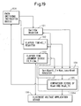
- FIG. 19 is a block diagram of the configuration of a control system of a multichannel optical switch according to Example 4 of the present invention.
- an Sw register 191, EI_T register 192, and EI_T ⁇ m_TH comparison device 193 are the same as the Sw register 151, EI_T register 152, and EI_T ⁇ m_TH comparison device 153 in Example 2 shown in FIG. 15.
- the electrode voltage application device 106 of FIG. 10 is realized in Example 4 by an electrode voltage application device 196.
- the point of difference with Example 2 shown in FIG. 15 is that, in Example 4, the switching judgment processing device 1052 in Example 2 is replaced with a switching judgment processing device 1054 of a different configuration.
- the rest of the configuration is the same as Example 2.
- the switching judgment processing device 1054 in Example 4 is provided with a unit time wattage storage register (WswA register) 194 for storing a WswA value obtained by subtracting from a product of a switching count Sw and a coefficient Wsw for deriving the amount of heat generation envisioned from that switching count Sw (coefficient for conversion of wattage generated there based on Sw) the product of the elapsed time EL_T and a coefficient Wsw_loss for deriving the amount of natural heat generation envisioned from the elapsed time EL_T (coefficient for conversion of wattage discharged there based on EL_T) when the elapsed time judgment device 193 judges that a predetermined counted time threshold Am_T has been exceeded and a comparison device 195 for comparing the WswA value with a predetermined WswA threshold WswA_TH.
- WswA register unit time wattage storage register
- FIG. 20 is a flowchart for explaining the operation of the control system of a multichannel optical switch according to Example 4 shown in FIG. 19.
- step 201 to step 204 are the same as step 161 to step 164 in Example 2 shown in FIG. 16.
- the explanations will be omitted.
- the WswA register 194 inside the switching judgment processing device 1054 subtracts from a product of a switching count Sw and a coefficient Wsw for deriving the amount of heat generation envisioned from that switching count Sw the product of the elapsed time EL_T and a coefficient Wsw_loss for deriving the amount of natural heat generation envisioned from the elapsed time EL_T when the elapsed time judgment device 193 judges that a predetermined counted time threshold Am_T has been exceeded. Further, the control system records the obtained WSwA value in the WswA register 194.
- step 206 it for example clears the value of the Sw register 191 and the value of the EL_T register 192 to 0 to initialize them when the above subtraction ends.
- step 207 it compares the WSwA value and the predetermined WswA threshold WswA_TH by the comparison device 195.
- the WSwA value is smaller than the predetermined WswA threshold WswA_TH
- step 208 it applies voltage for switching the optical switch devices based on the switching data to the optical switch devices.
- the WSwA value is the predetermined WswA threshold WswA_TH or more, at step 209, it stops the application of the electrode voltage and, at step 210, sends a switching failure notice to the response input port 123 inside the path switching instruction device 801.
- FIG. 21 is a block diagram of the configuration of a control system of a multichannel optical switch according to Example 5 of the present invention.
- the switching data input device 101 of FIG. 10 is realized in Example 5 by a switching data input device 1015 and is provided with an applied voltage register for temporarily storing a working channel applied voltage V 1 for the optical switch device of a working channel, a preceding channel applied voltage V 1 - for the optical switch device of the preceding channel adjoining the working channel (for example, if the working channel is CH3, the adjoining preceding channel would be CH2), and a succeeding channel applied voltage V 1+ for the optical switch device of the succeeding channel adjoining the working channel (for example, if the working channel is CH3, the adjoining succeeding channel would be CH4).
- the judgment data recording device 103 of FIG. 10 is realized by a judgment data recording device 1035 and is provided with a register 2110 for storing a preceding adjoining channel voltage difference Vtc1 between a working channel applied voltage V 1 and a preceding channel applied voltage V 1 - and a succeeding adjoining channel voltage difference Vtc2 between the applied voltage V 1 and the applied voltage V 1+ , a comparison device 2111 for comparing the absolute value of the preceding adjoining channel voltage difference Vtc1 and the absolute value of the succeeding adjoining channel voltage difference Vtc2, a conversion device 2112 for converting the greater adjoining channel voltage difference among the absolute value of the preceding adjoining channel voltage difference Vtc1 and the absolute value of the succeeding adjoining channel voltage difference Vtc2 into an adjoining channel voltage difference value Vtc, and a Vtcm register 2113 for adding an adjoining channel voltage difference value Vtc to the adjoining channel difference sum Vtcm to update the adjoining channel difference sum.
- a register 2110 for storing
- the elapsed time recording device 102 of FIG. 10 is realized by an elapsed time recording register (EL_T register) 2114 for recording the elapsed time EL_T, while the elapsed time judgment device of FIG. 10 is realized by a comparison device 2115 for judging whether EI_T ⁇ Am_TH.
- EL_T register elapsed time recording register
- the switching judgment processing device 1055 is provided with a unit time adjoining channel potential difference storage register (VtcmA register) 2116 for storing the value VtcmA obtained by dividing the Vtcm value by the elapsed time EL_T when the elapsed time judgment device 2115 judges that the predetermined counted time threshold Am_T has been exceeded and a comparison device 2117 for comparing the VtcmA value and a predetermined electrode voltage application judgment threshold VtcmA_TH.
- the electrode voltage application device 106 of FIG. 10 is realized in Example 5 by an electrode voltage application device 2117.
- the values of the EL_T register 2114 and Vtcm register 2113 are cleared to 0 to be initialized when the division for obtaining the VtcmA value ends.
- the electrode voltage application device 106 applies voltage for switching the optical switch devices based on switching data to the optical switch devices of the optical switches.
- the VtcmA value is the predetermined electrode voltage application judgment threshold VtcmA_TH or more, it sends a switching failure notice to the path switching instruction device 801.
- FIG. 22 is a flowchart for explaining operation of the control system of a multichannel optical switch according to Example 5 shown in FIG. 21.
- the system inputs switching data from the switching data output port 111 to the path switching instruction device 801 and, at step 2211, records the working channel applied voltage V 1 to the optical switch device of the working channel, the preceding channel applied voltage V 1 - to the optical switch device of the preceding channel next to the working channel, and the succeeding channel applied voltage V 1+ to the optical switch device of the succeeding channel next to the working channel in the applied voltage register 1012.
- step 2212 it stores the preceding adjoining channel voltage difference Vtc1 of the working channel applied voltage V 1 and the preceding channel applied voltage V 1 - and the succeeding adjoining channel voltage difference Vtc2 of the applied voltage V 1 and applied voltage V 1+ in the register 2110.
- the system uses the comparison device 2111 to compare the absolute value of the preceding adjoining channel voltage difference Vtc1 and the absolute value of the succeeding adjoining channel voltage difference Vtc2. If the result of the comparison is
- , at step 2214, it uses the conversion device 2112 to convert this to Vtc1 Vtc, while if the result is
- the system records the elapsed time EL_T from when the switching data starts to be output from the path switching instruction device 801 in the EI_T register 2114.
- the system uses the elapsed time judgment device 2115 to compare the elapsed time EL_T and the predetermined threshold Am_TH. If EL_TH ⁇ Am_TH, then at step 2219, it supplies voltage to the electrodes of the corresponding optical switch devices. If EL_TH ⁇ Am_TH, then at step 2220, it records the value VtcmA obtained by dividing Vtcm by the elapsed time EL_T in the unit time adjoining channel potential difference storage register (VtcmA) 2116. Next, at step 2221, it for example clears the values of the ET_T register 2114 and the Vtcm register 2113 to 0 to initialize them.
- the system uses the comparison device 2117 to compare the VtcmA value and the electrode voltage application judgment threshold VtcmA_TH. If VtcmA ⁇ VtcmA_TH, at step 2219, it supplies voltage to the electrodes of the corresponding optical switch devices. If VtcmA ⁇ VtcmA_TH, at step 2223, it stops application of the electrode voltage and, at step 2224, notifies switching failure to the response input port 123 of the path switching instruction device 801.
- FIG. 23 is a block diagram of the configuration of a control system of a multichannel optical switch according to Example 6 of the present invention.
- a switching data input device 1016 is the same as the switching data input device 1015 in Example 5.
- the explanation will be omitted.
- a judgment data recording device 1036 is provided with a register 2310 the same as the register 2110 in Example 5, a comparison device 2311 for comparing the absolute value of the preceding adjoining channel voltage difference Vtc1 and the adjoining channel difference threshold Vtc_TH, a comparison device 2312 for comparing the absolute value of the succeeding adjoining channel voltage difference Vtc2 and the adjoining channel difference threshold Vtc_TH, and a switching count storage register (Sw register) 2313 serving as a counter incremented by 1 when the absolute value of the preceding adjoining channel voltage difference Vtc1 is the adjoining channel difference threshold Vtc_TH or more and the absolute value of the succeeding adjoining channel voltage difference Vtc2 is the adjoining channel difference threshold Vtc_TH or more.
- Sw register switching count storage register
- the elapsed time recording device 102 in FIG. 10 is realized in Example 6 by an EL_T register 2314 for recording the elapsed time EL_T if the absolute value of the preceding adjoining channel voltage difference Vtc1 is less than the adjoining channel difference threshold Vtc_TH and the absolute value of the succeeding adjoining channel voltage difference Vtc2 is less than the adjoining channel difference threshold Vtc_TH, while the elapsed time judgment device 104 in FIG. 10 is realized by a comparison device 2315, the same as the comparison device 2115 in Example 5, for judging EI_T ⁇ Am_TH.
- the switching judgment processing device 105 in FIG. 10 is realized in Example 6 by a switching judgment processing device 1056 and is provided with an inter-channel leak processing Sw recording register (unit time switching count storage register) (SwcA register) 2316 for storing the value SwcA obtained by dividing the Sw value by the elapsed time EL_T when the elapsed time judgment device 2315 judges that the elapsed time EL_T has exceeded a predetermined counted time threshold Am_T and a comparison device 2317 for comparing the SwcA value and a predetermined electrode voltage application judgment threshold (adjoining channel potential difference threshold) SwcA_TH.
- an inter-channel leak processing Sw recording register unit time switching count storage register
- SwcA register unit time switching count storage register
- the values of the EL_T register 2314 and Sw register 2313 are for example cleared to 0 to be initialized when the above division for obtaining the SwcA value ends.
- the electrode voltage application device 106 applies voltage for switching the optical switch devices based on the switching data to the optical switch devices when the SwcA value is smaller than a predetermined electrode voltage application judgment threshold SwcA_TH and sends a switching failure notice to the path switching instruction device 801 when the SwcA value is the predetermined electrode voltage application judgment threshold SwcA_TH or more.
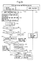
- FIG. 24 is a flowchart for explaining the operation of the control system of a multichannel optical switch according to Example 6 shown in FIG. 23.
- the system inputs the switching data from the switching data output port 111 into the switching data input device 1012, while at step 242, it records the working channel applied voltage V 1 to the optical switch device of the working channel, the preceding channel applied voltage V 1 - to the optical switch device of the preceding channel adjoining the working channel, and the succeeding channel applied voltage V 1+ to the optical switch device of the succeeding channel adjoining the working channel in the applied voltage register 2110.
- step 243 the system records the preceding adjoining channel voltage difference Vtc1 between the working channel applied voltage V 1 and the preceding channel applied voltage V 1 -and the succeeding adjoining channel voltage difference Vtc2 between the applied voltage V 1 and the applied voltage V 1+ in the register 2110.
- the system uses the comparison device 2310 to compare the absolute value of the preceding adjoining channel voltage difference Vtc1 and the adjoining channel difference judgment threshold Vtc_TH. If the result of this comparison is lVtc1l ⁇ Vtc_TH, at step 245, it compares the absolute value of the succeeding adjoining channel voltage difference Vtc2 and the adjoining channel difference judgment threshold Vtc_TH. If the result of this comparison is also lVtc2l ⁇ Vtc_TH, the system does nothing, then at step 246, the system records the elapsed time EL_T from when the switching data started to be output from the path switching instruction device 801 in the elapsed time recording device (EI_T register) 102.
- EI_T register elapsed time recording device
- step 244 If, at step 244,
- step 248 it uses the elapsed time judgment device 104 to judge if EI_T ⁇ Am_TH. If the elapsed time EI_T is less than the predetermined threshold Am_TH, at step 2493, the system applies the electrode voltage, while if EI_T ⁇ Am_TH, at step 2494, it stops the application of the electrode voltage and, at step 2495, sends a switching failure notice to the response input port 123 of the path switching instruction device 801.
- FIG. 25 is a block diagram of the configuration of a control system of a multichannel optical switch according to Example 7 of the present invention.
- a switching data input device 1017 is the same as the switching data input device 1015 of Example 5 shown in FIG. 21.
- a judgment data recording device 1037 also has the same configuration as the judgment data recording device 1035 shown in Example 5 and is provided with a register 2510, comparison device 2511, conversion device 2512, and Vtcm register 2513.
- An elapsed time register 2514 and elapsed time judgment device 25 are the same as those in Example 5.
- a switching judgment processing device 1057 is provided with a unit time wattage storage register (WvtcmA register) 2516 for storing a WvtcmA value obtained by subtracting from a product of an adjoining channel voltage difference Vtcm and a coefficient Wvtc for deriving the amount of heat generation envisioned from that adjoining channel difference voltage difference Vtcm (coefficient for conversion of wattage generated there based on Vtcm) the product of the elapsed time EL_T and a coefficient Wvtc_loss for deriving the amount of natural heat generation envisioned from the elapsed time EL T (coefficient for conversion of wattage not generating heat there based on EL_T) when the elapsed time judgment device 2515 judges that the predetermined counted time threshold Am_T has been exceeded and a comparison device 2517 for comparing the WvtcmA value with a predetermined WvtcmA threshold WvtcmA_TH.
- the system for example clears the value of the Vtcm register 2113 and the value of the EL_T register 2514 to the initial value of 0 when the subtraction for obtaining WvtcmA ends.
- An electrode voltage application device 2519 applies voltage for switching the optical switch devices based on the switching data to the optical switch devices when the WvtcmA value is smaller than a predetermined electrode voltage application judgment WvtcmA threshold WvtcmA_TH and sends a switching failure notice to the path switching instruction device 801 when the WvtcmA value is the predetermined WvtcmA threshold WvtcmA_TH or more.
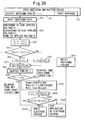
- FIG. 26 is a flowchart for explaining the operation of the control system of a multichannel optical switch according to Example 7 shown in FIG. 25.
- step 261 to step 269 are the same as step 2210 to step 2218 in Example 5 shown in FIG. 22.
- the explanations will be omitted.
- Example 7 at step 2691, the system subtracts from a product of an adjoining channel voltage difference Vtcm and a coefficient Wvtc for deriving the amount of heat generation envisioned from that adjoining channel difference voltage difference Vtcm the product of the elapsed time EL_T and a coefficient Wvtc_loss for deriving the amount of natural heat generation envisioned from the elapsed time EL_T.
- step 2692 it for example clears the contents of the Vtcm register 2113 and the EI_T register 2114 to 0 to initialize them.
- step 2693 uses the comparison device 2517 to compare WcmA and WcmA_TH.
- step 2694 the system applies the electrode voltage. If WcmA ⁇ WcmA_TH, then at step 2695, the system stops the application of the electrode voltage and, at step 2697, sends a switching failure notice to the response input port 123 of the path switching instruction device 801.
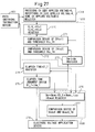
- FIG. 27 is a block diagram of the configuration of a control system of a multichannel optical switch according to Example 8 of the present invention.
- a switching data input device 1018 is the same as the switching data input device 1016 of Example 6 shown in FIG. 23.
- a judgment data recording device 1038 also has the same configuration as the judgment data recording device 1036 shown in Example 6 and is provided with a register 270, comparison device 271, conversion device 272, and Sw register 273 serving as the switching count counter.
- An elapsed time register 274 and elapsed time judgment device 275 are also the same as those in Example 6.
- the switching judgment processing device 105 in FIG. 10 is realized by a switching judgment processing device 1058 and is provided with a unit time wattage storage register (WswcA register) 276 for storing the WswcA value obtained by subtracting from the product of a switching count Sw and a coefficient Wswc for deriving an amount of heat generation envisioned from the switching count Sw a product of an elapsed time EL_T and a coefficient Wswc_loss for deriving an amount of natural heat generation envisioned from the elapsed time EL_T when the elapsed time judgment device 275 judges that the predetermined counted time threshold Am_T has been exceeded and a comparison device 277 for comparing the WswcA value with a predetermined wattage threshold (WswcA threshold) WswcA_TH.
- WswcA register unit time wattage storage register
- the value of the Sw register 273 and the value of the EL_T register are for example cleared to 0 to be initialized when the subtraction for obtaining the WswcA value ends.
- An electrode voltage application device 278 applies a voltage for switching the optical switch devices based on the switching data to the optical switch devices when the WswcA value is smaller than a predetermined WswcA threshold WswcA_TH and sends a switching failure notice to the path switching instruction device when the WswcA value is the predetermined WswcA threshold WswA Th or more.
- FIG. 28 is a flowchart for explaining the operation of the control system of a multichannel optical switch according to Example 8 shown in FIG. 27.
- steps 281 to 288 are the same as steps 241 to 248 in Example 6 shown in FIG. 24.
- the explanations are omitted.
- the system stores the WswcA value, obtained by subtracting from the product of a switching count Sw and a coefficient Wswc for deriving an amount of heat generation envisioned from the switching count Sw a product of an elapsed time EL_T and a coefficient Wswc_loss for deriving an amount of natural heat generation envisioned from the elapsed time EL_T when the elapsed time judgment device 275 judges that a predetermined counted time threshold Am_T has been exceeded, in the WawcA register 276.
- the system clears the values of the Sw register 273 and the EI_T register 274 to 0 and, at step 2893, judges if WxwcA ⁇ WswcA_TH by the comparison device 277. If WxwcA ⁇ WswcA_TH, then at step 2893, the system applies the electrode voltage, while if Wxwc ⁇ WswcA_TH, then at step 2894, it stops the application of the electrode voltage and, at step 2895, sends a switching failure notice to the response input port 123 of the path switching instruction device 801.
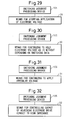
- FIG. 29 is a view showing a means 29 for stopping the application of the electrode voltage when the judgment in the switching judgment processing device in Examples 1 to 8 of the present invention is that the value is a predetermined threshold or more shown in the figure.
- FIGS. 30 to 32 are views showing examples of using other means in place of the means 29 in Examples 1 to 8 by Example 9 of the present invention. That is, the present invention is not limited to the means 29 shown in FIG. 29. According to Example 9 of the present invention, as shown in FIG. 30, instead of stopping the application of the electrode voltage, it is also possible to prevent the electrode voltage from changing by a means 30 for continuing to hold the electrode voltage as it is without relying on the switching data.
- a means 31 for continuing to apply an irregular voltage instead of stopping the application of the electrode voltage as a result of the judgment at the switching judgment processing device 105 in Examples 1 to 8 of the present invention, it is also possible to provide a means 31 for continuing to apply an irregular voltage.
- the input channel is the channel 1
- Examples 5 to 8 instead of stopping the application of the electrode voltage, it is also possible to provide a means 32 for controlling the output of the drive circuit of the adjoining electrode to a high impedance and thereby suppress the generation of leakage current between the wires and notify switching failure of the adjoining channel to the path switching instruction device 801.
- FIG. 33 is a block diagram of part of the configuration of the control system of a multichannel optical switch according to Example 10 of the present invention.
- the system is provided with a predicted reconnection time notification means 33 for notifying a certain restrictive condition for allowing acceptance of switching when it uses the switching judgment processing device 105 to send a switching failure notice to the path switching instruction device 801. Due to this, it narrows down the switching data from the path switching instruction device 801 and lightens the load of the switch by a certain switching restriction.
- FIG. 34 is a block diagram of part of the configuration of the control system of a multichannel optical switch according to Example 11 of the present invention.
- the system uses data on the combination of paths allowing switching or data on the time interval of the input of switching data allowing switching as the "certain restrictive condition" in Example 10 and is provided with a switching acceptance allowance data notification means 34 for notifying this data.
- FIG. 35 is a table for explaining the relationship between the input/output channels and the unit voltage for explaining Example 12 of the present invention
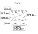
- FIG. 36 is a diagram for explaining the relationship of direction of the path and the sign of the unit voltage based on the table shown in FIG. 35.
Landscapes
- Engineering & Computer Science (AREA)
- Computer Networks & Wireless Communication (AREA)
- Optical Modulation, Optical Deflection, Nonlinear Optics, Optical Demodulation, Optical Logic Elements (AREA)
Applications Claiming Priority (1)
| Application Number | Priority Date | Filing Date | Title |
|---|---|---|---|
| JP2006221252A JP2008046316A (ja) | 2006-08-14 | 2006-08-14 | 多チャンネル光スイッチの制御装置 |
Publications (1)
| Publication Number | Publication Date |
|---|---|
| EP1912465A2 true EP1912465A2 (de) | 2008-04-16 |
Family
ID=38664420
Family Applications (1)
| Application Number | Title | Priority Date | Filing Date |
|---|---|---|---|
| EP07007869A Withdrawn EP1912465A2 (de) | 2006-08-14 | 2007-04-18 | Steuerungssystem eines optischen Mehrkanalvermittlers |
Country Status (3)
| Country | Link |
|---|---|
| US (1) | US20080166121A1 (de) |
| EP (1) | EP1912465A2 (de) |
| JP (1) | JP2008046316A (de) |
Families Citing this family (1)
| Publication number | Priority date | Publication date | Assignee | Title |
|---|---|---|---|---|
| US20140297038A1 (en) * | 2013-03-29 | 2014-10-02 | Raytheon Bbn Technologies Corp. | Network, control system for controlling the network, network apparatus for the network, and method of controlling the network |
Family Cites Families (3)
| Publication number | Priority date | Publication date | Assignee | Title |
|---|---|---|---|---|
| EP0782017B1 (de) * | 1995-12-28 | 2009-08-05 | Panasonic Corporation | Optischer Wellenleiter, Vorrichtung zur Umwandlung optischer Wellenlängen und Verfahren zu ihrer Herstellung |
| JP2003021795A (ja) * | 2001-07-09 | 2003-01-24 | Nec Corp | 光スイッチシステム |
| US7274841B2 (en) * | 2002-10-23 | 2007-09-25 | Japan Science And Technology Agency | Optical signal amplifying triode and optical signal transfer method, optical signal relay device, and optical signal storage device using the same |
-
2006
- 2006-08-14 JP JP2006221252A patent/JP2008046316A/ja not_active Withdrawn
-
2007
- 2007-04-18 EP EP07007869A patent/EP1912465A2/de not_active Withdrawn
- 2007-04-19 US US11/785,658 patent/US20080166121A1/en not_active Abandoned
Also Published As
| Publication number | Publication date |
|---|---|
| US20080166121A1 (en) | 2008-07-10 |
| JP2008046316A (ja) | 2008-02-28 |
Similar Documents
| Publication | Publication Date | Title |
|---|---|---|
| US8848322B2 (en) | Gate control circuit, power module and associated method | |
| KR101943882B1 (ko) | Mmc 컨버터의 서브모듈 제어기용 전원장치 | |
| US20120020137A1 (en) | Power conversion device | |
| US6657838B2 (en) | LCD backlight inverter | |
| CN101627502A (zh) | 电隔离的充电平衡系统 | |
| US10587258B2 (en) | Drive circuit of power semiconductor switch | |
| JPWO2013118271A1 (ja) | 並列蓄電システムおよびその制御方法 | |
| EP1912465A2 (de) | Steuerungssystem eines optischen Mehrkanalvermittlers | |
| JP2020013656A (ja) | 直流電流遮断装置 | |
| EP3220528A1 (de) | Stromwandlungsvorrichtung | |
| CN108400394B (zh) | 电池管理系统的电子开关装置以及电池 | |
| US20150064587A1 (en) | Apparatus and method for controlling fuel cell system using sub-power conditioning system | |
| US8482328B2 (en) | Switching device and method for preventing malfunction of the same | |
| US20090244674A1 (en) | Mirror driving circuit and optical switch | |
| CN105122648A (zh) | 切换导体器件的方法 | |
| KR20140127677A (ko) | 스위칭 증폭기 장치 및 그 제어 방법 | |
| US20070092763A1 (en) | Fuel cell system | |
| US8184421B2 (en) | Power converter | |
| KR102573440B1 (ko) | 반도체 스위치를 이용한 펄스 전원 장치 및 이의 고속 게이트 제어 방법 | |
| JP5638194B2 (ja) | 電力用半導体素子のゲート回路 | |
| US20140354060A1 (en) | Power supply apparatus and electronic apparatus having the same | |
| JP7303308B2 (ja) | 高速度直流真空遮断器 | |
| CN119856399A (zh) | 具有一个或多个常通栅极的叠接装置 | |
| US10075123B2 (en) | Semiconductor device, motor control system, and control method for semiconductor device | |
| KR100581490B1 (ko) | 고압 스위칭 시스템의 구동 시스템 |
Legal Events
| Date | Code | Title | Description |
|---|---|---|---|
| PUAI | Public reference made under article 153(3) epc to a published international application that has entered the european phase |
Free format text: ORIGINAL CODE: 0009012 |
|
| AK | Designated contracting states |
Kind code of ref document: A2 Designated state(s): AT BE BG CH CY CZ DE DK EE ES FI FR GB GR HU IE IS IT LI LT LU LV MC MT NL PL PT RO SE SI SK TR |
|
| AX | Request for extension of the european patent |
Extension state: AL BA HR MK RS |
|
| STAA | Information on the status of an ep patent application or granted ep patent |
Free format text: STATUS: THE APPLICATION HAS BEEN WITHDRAWN |
|
| 18W | Application withdrawn |
Effective date: 20090415 |