EP1912332A2 - Logic gate, scan driver and organic light emitting diode display using the same - Google Patents
Logic gate, scan driver and organic light emitting diode display using the same Download PDFInfo
- Publication number
- EP1912332A2 EP1912332A2 EP07114023A EP07114023A EP1912332A2 EP 1912332 A2 EP1912332 A2 EP 1912332A2 EP 07114023 A EP07114023 A EP 07114023A EP 07114023 A EP07114023 A EP 07114023A EP 1912332 A2 EP1912332 A2 EP 1912332A2
- Authority
- EP
- European Patent Office
- Prior art keywords
- driver
- transistor
- terminal
- electrode
- gate electrode
- Prior art date
- Legal status (The legal status is an assumption and is not a legal conclusion. Google has not performed a legal analysis and makes no representation as to the accuracy of the status listed.)
- Granted
Links
- 239000003990 capacitor Substances 0.000 claims abstract description 10
- 238000004519 manufacturing process Methods 0.000 description 9
- 238000000034 method Methods 0.000 description 6
- 241001269238 Data Species 0.000 description 2
- 230000003071 parasitic effect Effects 0.000 description 2
- 101150070189 CIN3 gene Proteins 0.000 description 1
- 101150110971 CIN7 gene Proteins 0.000 description 1
- 101100286980 Daucus carota INV2 gene Proteins 0.000 description 1
- 101100508840 Daucus carota INV3 gene Proteins 0.000 description 1
- 101150110298 INV1 gene Proteins 0.000 description 1
- 101100397044 Xenopus laevis invs-a gene Proteins 0.000 description 1
- 101100397045 Xenopus laevis invs-b gene Proteins 0.000 description 1
- 239000004973 liquid crystal related substance Substances 0.000 description 1
- 238000012986 modification Methods 0.000 description 1
- 230000004048 modification Effects 0.000 description 1
- 238000005215 recombination Methods 0.000 description 1
- 230000006798 recombination Effects 0.000 description 1
Images


Classifications
-
- G—PHYSICS
- G09—EDUCATION; CRYPTOGRAPHY; DISPLAY; ADVERTISING; SEALS
- G09G—ARRANGEMENTS OR CIRCUITS FOR CONTROL OF INDICATING DEVICES USING STATIC MEANS TO PRESENT VARIABLE INFORMATION
- G09G3/00—Control arrangements or circuits, of interest only in connection with visual indicators other than cathode-ray tubes
- G09G3/20—Control arrangements or circuits, of interest only in connection with visual indicators other than cathode-ray tubes for presentation of an assembly of a number of characters, e.g. a page, by composing the assembly by combination of individual elements arranged in a matrix no fixed position being assigned to or needed to be assigned to the individual characters or partial characters
- G09G3/22—Control arrangements or circuits, of interest only in connection with visual indicators other than cathode-ray tubes for presentation of an assembly of a number of characters, e.g. a page, by composing the assembly by combination of individual elements arranged in a matrix no fixed position being assigned to or needed to be assigned to the individual characters or partial characters using controlled light sources
- G09G3/30—Control arrangements or circuits, of interest only in connection with visual indicators other than cathode-ray tubes for presentation of an assembly of a number of characters, e.g. a page, by composing the assembly by combination of individual elements arranged in a matrix no fixed position being assigned to or needed to be assigned to the individual characters or partial characters using controlled light sources using electroluminescent panels
-
- H—ELECTRICITY
- H03—ELECTRONIC CIRCUITRY
- H03K—PULSE TECHNIQUE
- H03K19/00—Logic circuits, i.e. having at least two inputs acting on one output; Inverting circuits
- H03K19/02—Logic circuits, i.e. having at least two inputs acting on one output; Inverting circuits using specified components
- H03K19/08—Logic circuits, i.e. having at least two inputs acting on one output; Inverting circuits using specified components using semiconductor devices
- H03K19/094—Logic circuits, i.e. having at least two inputs acting on one output; Inverting circuits using specified components using semiconductor devices using field-effect transistors
- H03K19/0944—Logic circuits, i.e. having at least two inputs acting on one output; Inverting circuits using specified components using semiconductor devices using field-effect transistors using MOSFET or insulated gate field-effect transistors, i.e. IGFET
- H03K19/09441—Logic circuits, i.e. having at least two inputs acting on one output; Inverting circuits using specified components using semiconductor devices using field-effect transistors using MOSFET or insulated gate field-effect transistors, i.e. IGFET of the same canal type
-
- G—PHYSICS
- G09—EDUCATION; CRYPTOGRAPHY; DISPLAY; ADVERTISING; SEALS
- G09G—ARRANGEMENTS OR CIRCUITS FOR CONTROL OF INDICATING DEVICES USING STATIC MEANS TO PRESENT VARIABLE INFORMATION
- G09G3/00—Control arrangements or circuits, of interest only in connection with visual indicators other than cathode-ray tubes
- G09G3/20—Control arrangements or circuits, of interest only in connection with visual indicators other than cathode-ray tubes for presentation of an assembly of a number of characters, e.g. a page, by composing the assembly by combination of individual elements arranged in a matrix no fixed position being assigned to or needed to be assigned to the individual characters or partial characters
- G09G3/22—Control arrangements or circuits, of interest only in connection with visual indicators other than cathode-ray tubes for presentation of an assembly of a number of characters, e.g. a page, by composing the assembly by combination of individual elements arranged in a matrix no fixed position being assigned to or needed to be assigned to the individual characters or partial characters using controlled light sources
- G09G3/30—Control arrangements or circuits, of interest only in connection with visual indicators other than cathode-ray tubes for presentation of an assembly of a number of characters, e.g. a page, by composing the assembly by combination of individual elements arranged in a matrix no fixed position being assigned to or needed to be assigned to the individual characters or partial characters using controlled light sources using electroluminescent panels
- G09G3/32—Control arrangements or circuits, of interest only in connection with visual indicators other than cathode-ray tubes for presentation of an assembly of a number of characters, e.g. a page, by composing the assembly by combination of individual elements arranged in a matrix no fixed position being assigned to or needed to be assigned to the individual characters or partial characters using controlled light sources using electroluminescent panels semiconductive, e.g. using light-emitting diodes [LED]
- G09G3/3208—Control arrangements or circuits, of interest only in connection with visual indicators other than cathode-ray tubes for presentation of an assembly of a number of characters, e.g. a page, by composing the assembly by combination of individual elements arranged in a matrix no fixed position being assigned to or needed to be assigned to the individual characters or partial characters using controlled light sources using electroluminescent panels semiconductive, e.g. using light-emitting diodes [LED] organic, e.g. using organic light-emitting diodes [OLED]
- G09G3/3266—Details of drivers for scan electrodes
-
- G—PHYSICS
- G09—EDUCATION; CRYPTOGRAPHY; DISPLAY; ADVERTISING; SEALS
- G09G—ARRANGEMENTS OR CIRCUITS FOR CONTROL OF INDICATING DEVICES USING STATIC MEANS TO PRESENT VARIABLE INFORMATION
- G09G2310/00—Command of the display device
- G09G2310/06—Details of flat display driving waveforms
Abstract
Description
- The present invention relates to a logic gate capable of being realized using MOS transistors of a single type only and a scan driver and an organic light emitting display using the logic gate, and more specifically to a logic gate capable of being realized with PMOS transistors and a scan driver and an organic light emitting display using the logic gate.
- In recent years, various types of flat panel displays having reduced weight and volume which are disadvantages of cathode ray tubes (CRTs) have been developed. The types of flat panel displays include liquid crystal displays (LCDs), field emission displays (FEDs), plasma display panels (PDPs), organic light emitting diode displays (OLEDs), etc.
- The OLED displays an image using organic light emitting diodes which generate light by means of recombination of electrons and holes. Such an organic light emitting display device has an advantage in that it has a rapid response time and consumes low power.
- Generally, an OLED display includes pixels arranged in a matrix-type manner, a data driver for driving data lines connected to the pixels, and a scan driver for driving scan lines connected to the pixels.
- The data driver supplies a data signal to the pixels selected by a scan signal provided by the scan driver. Therefore, each of the pixels displays a predetermined image corresponding to the data signal by supplying a predetermined electric current, corresponding to the data signal, to an organic light emitting diode.
- It is desirable to mount the scan driver on the panel to reduce the manufacturing cost of the OLED. However, it is difficult to do so since the conventional scan driver is composed of PMOS transistors and NMOS transistors. That is to say, the problem is that the number of masks and thus of the production steps required will increase when the scan driver composed of PMOS and NMOS transistors is formed on the panel. Accordingly, there has been demand for a scan driver capable of being realized with MOS transistors of a single polarity type only in order to be able to form it on a panel.
- Accordingly, the present invention is designed to solve such drawbacks of the prior art, and therefore an object of the present invention is to provide a logic gate capable of being realized with MOS transistors of a single polarity type, a scan driver and an organic light emitting display using the same.
- Accordingly, a first aspect of the present invention provides a logic gate comprising a first power source, a second power source, a plurality of input terminals, a first driver, a second driver, a third driver, a control transistors, a first capacitor, and a fourth driver. The first power source is adapted to provide a first power supply voltage and the second power source is adapted to provide a second power supply voltage, different from the first power supply voltage. The plurality of input terminals is adapted to receive a plurality of input signals. The first driver has a first terminal connected to the first power source, a second terminal connected to a first node, and a plurality of inputs, each of the plurality of inputs being connected to a corresponding one of the plurality of input terminals. The second driver has a first terminal connected to the first node, and a second terminal connected to the second power source. The third driver has a first terminal connected to the first power source, an input connected to the first node, and an output terminal. The control transistor has a first electrode connected to the output terminal of the third driver, a second electrode connected to the second power source, and a gate electrode. The fourth driver has a first terminal connected to the gate electrode of the control transistor and a second terminal connected to the second power source. The first capacitor has a first terminal connected to the first electrode of the control transistor and a second terminal connected to the gate electrode of the control transistor.
- The first driver is adapted to provide the first power supply voltage to the first node corresponding to a logic combination of the plurality of input signals and the second driver is adapted to provide the second power supply voltage to the first node when the first driver does not provide the first power supply voltage to the first node. The third driver is adapted to provide the first power supply voltage to the output terminal when the second power supply voltage is provided to the first node and the fourth driver is adapted to provide the second power supply voltage to the gate electrode of the control transistor when the third driver does not provide the first power supply voltage to the output terminal. Each of the first driver, the second driver, the third driver, and the fourth driver comprises at least one transistor. These transistors and the control transistor are MOS transistors of the same polarity type.
- The OR-gate of the first aspect of the invention has an advantage in that in comprises transistors only of a single polarity type, preferably PMOS transistors, and therefore can be integrated into the display panel of an OLED display device without increasing the number of production steps and therefore production cost.
- A second aspect of the invention provides a scan driver scan driver comprising at least one decoder having a plurality of first OR gates according to first aspect of the invention and a plurality of second OR gates, also according to the first aspect of the invention. Each of the plurality of input terminals of any of the plurality of second OR gates is connected to an output terminal of one of the plurality of first OR gates of any one of the at least one decoders. The scan driver of the second aspect of the invention has an advantage in that it can be integrated into the display panel of an OLED display device without increasing the number of production steps and therefore production cost.
- A third aspect of the invention provides an OLED display device comprising a scan driver according to the second aspect of the invention.
- These and/or other aspects and advantages of the invention will become apparent and more readily appreciated from the following description of the preferred embodiments, taken in conjunction with the accompanying drawings of which:
- FIG. 1 illustrates a circuit view of an OR gate according to the first embodiment of the present invention,
- FIG. 2 illustrates a circuit view of an OR gate according to the second embodiment of the present invention,
- FIG. 3 illustrates a circuit view of an OR gate according to the third embodiment of the present invention,
- FIG. 4 illustrates a circuit view of an OR gate according to the fourth embodiment of the present invention,
- FIG. 5 illustrates a circuit view of an OR gate according to the fifth embodiment of the present invention,
- FIG. 6 illustrates a circuit view of a scan driver according to one embodiment of the present invention,
- FIG. 7 illustrates driving waveforms according to an embodiment of the present invention,
- FIG. 8 illustrates a circuit view of an example of a connection procedure of the first OR gates as shown in FIG. 6,
- FIG. 9A illustrates a detailed view of driving waveforms according to an embodiment of the present invention,
- FIG. 9B illustrates driving waveforms according to another embodiment of the present invention,
- FIG. 10 illustrates a schematic view of an organic light emitting diode display according to an embodiment of the present invention.
- Hereinafter, preferable embodiments of the present invention will be described with reference to the accompanying drawings, as apparent to those skilled in the art. Here, when one element is described as being connected to a second element, the element may be directly connected to the second element but also indirectly via another, third, element. Further, irrelative elements may be omitted for clarity. Like reference numerals refer to like elements throughout.
- FIG. 1 is a circuit view showing an OR gate according to the first embodiment of the present invention. Here, the OR gate according to the first embodiment of the present invention is realized with PMOS transistors.
- Referring to FIG. 1, the OR gate according to the first embodiment of the present invention comprises an eighth transistor (M8) (a control transistor) for controlling the voltage supplied to an output terminal (Vout); a
first driver 10 arranged between a first power source (VDD) and a first node (N1) and controlling the connection of the first node (N1) to the first power source (VDD) to correspond to polarities (HIGH or LOW) of a first input signal (IN1), a second input signal (IN2) and a third input signal (IN3); asecond driver 12 arranged between the first node (N1) and a second power source (VSS) to control the voltage of the first node (N1); athird driver 14 connected between a first electrode of the eighth transistor (M8) and the first power source (VDD) and controlling the connection of the first power source (VDD) to the first electrode of the eighth transistor (M8) to correspond to the voltage of the first node (N1); and afourth driver 16 connected between a gate electrode of the eighth transistor (M8) and the second power source (VSS) and controlling the connection of the second power source (VSS) to the gate electrode of the eighth transistor (M8) to correspond to polarities (HIGH or LOW) of the first input signal (IN1), the second input signal (IN2) and the third input signal (IN3). - The second driver can be realized in at least one of two different ways, the first one being depicted in FIGS. 1, 2, and 4, the second one in FIGS. 3 and 5. The third driver can be realized in at least three different ways, the first being depicted in FIG. 2, the second in FIGS. 1 and 3, and the third being depicted in FIGS. 4 and 5. The fourth driver can be realized in at least two different way, the first being illustrated in FIG. 2, the second being illustrated in FIGS. 1, 3, 4, and 5. Thus, the present invention discloses no less than twelve different combinations of the second, third, and fourth drivers from which the person skilled in the art may choose according to circumstances of the specific implementation. Only five of the combinations are illustrated by one of the FIGS. 1 through 5, however, the remaining combinations are not to be excluded from the scope of the document.
- The eighth transistor (M8) controls the voltage supplied to an output terminal (Vout) while being turned on or turned off by the voltage supplied to its gate electrode. For example, the eighth transistor (M8) is turned off when the voltage of the first power source (VDD) is supplied to its gate electrode, and turned on when the voltage of the second power source (VSS) is supplied to its gate electrode.
- The
first driver 10 includes a first transistor (M1), a second transistor (M2) and a third transistor (M3), which are connected in series between the first power source (VDD) and the first node (N1). In such afirst driver 10, the first power source (VDD) and the first node (N1) are electronically connected to each other when the first input signal (IN1), the second input signal (IN2) and the third input signal (IN3) are set to LOW polarity. - More specifically, the first transistor (M1) is turned on when the first input signal (IN1) has LOW polarity, the second transistor (M2) is turned on when the second input signal (IN2) has LOW polarity and, the third transistor (M3) is turned on when the third input signal (IN3) has LOW polarity. Here, since the first transistor (M1), the second transistor (M2) and the third transistor (M3) are connected in series between the first power source (VDD) and the first node (N1), the first power source (VDD) and the first node (N1) are electronically connected to each other when all of the first input signal (IN1), the second input signal (IN2) and the third input signal (IN3) have LOW polarity.
- The
second driver 12 includes a fourth transistor (M4) connected between the first node (N1) and the second power source (VSS); a fifth transistor (M5) connected between a gate electrode of the fourth transistor (M4) and a second power source (VSS); and a first capacitor (C1) connected between the gate electrode of the fourth transistor (M4) and a first electrode. Thesecond driver 12 maintains the voltage of the first power source (VDD) when the voltage of the first power source (VDD) is supplied to the first node (N1), and maintains the voltage of the first node (N1) at the voltage of the second power source (VSS) else. - More specifically, a first electrode of the fifth transistor (M5) is connected to the gate electrode of the fourth transistor (M4), and a gate electrode and a second electrode of the fifth transistor (M5) is connected to the second power source (VSS). That is to say, the fifth transistor (M5) is diode-connected to maintain the voltage of the gate electrode of the fourth transistor (M4) roughly at the voltage of the second power source (VSS).
- If the first power source (VDD) and the first node (N1) are electronically interrupted by the
first driver 10, then the fourth transistor (M4) maintains the voltage of the first node (N1) in LOW polarity (namely, the second power source (VSS)). And, if the first power source (VDD) and the first node (N1) are electronically connected to each other by thefirst driver 10, then the fourth transistor (M4) maintains the voltage of the first node (N1) in HIGH polarity (namely, the first power source (VDD)). For this purpose, a width/length ratio (W/L) of the fourth transistor (M4) is set to a narrower range than a width/length ratio (W/L) of each of the first transistor (M1), the second transistor (M2) and the third transistor (M3). - Therefore, the voltage of the first power source (VDD) may be stably maintained when the voltage of the first power source (VDD) is supplied to the first node (N1). Meanwhile, a predetermined leakage current may be caused by the fourth transistor (M4) when the voltage of the first power source (VDD) is supplied to the first node (N1). However, if the voltage of the first power source (VDD) is supplied to the first node (N1), then all of the first input signal (IN1), the second input signal (IN2) and the third input signal (IN3) have LOW polarity which happens in the scan driver according to the second aspect of the invention only during extremely short periods. Hence, power consumption is not unduly increased by the leakage current. Furthermore, the first capacitor (C1) charges the voltage between a first electrode and a gate electrode of a fourteenth transistor (M14), thereby to stabilize an operation of the fourth transistor (M14).
- The
third driver 14 includes a sixth transistor (M6) between the first power source (VDD) and a first electrode of the eighth transistor (M8); and a seventh transistor (M7) connected between a gate electrode and a second electrode of a sixth transistor (M6). Thethird driver 14 controls the connection of the first electrode of the eighth transistor (M8) to the first power source (VDD) to correspond to the voltage supplied to the first node (N1). - More specifically, the sixth transistor (M6) and the seventh transistor (M7) are turned on when the voltage of LOW polarity is supplied to the first node (N1), and turned off else. If the sixth transistor (M6) is turned on, then the voltage of the first power source (VDD) is supplied to the output terminal (Vout). If the seventh transistor (M7) is turned on, then a first electrode and a gate electrode of the eighth transistor (M8) are electronically connected to each other. That is to say, if the seventh transistor (M7) is turned on, then the voltage of the first power source (VDD) is supplied to the gate electrode of the eighth transistor (M8), and therefore the eighth transistor (M8) is turned off. Here, a second capacitor (C2) connected between the first electrode and the gate electrode of the eighth transistor (M8) charges the voltage between the first electrode and the gate electrode of the eighth transistor (M8), thereby to prevent a leakage current from being generated from the eighth transistor (M8).
- The
fourth driver 16 includes a ninth transistor (M9), a tenth transistor (M10) and an eleventh transistor (M11) which are all connected in series between the gate electrode of the eighth transistor (M8) and the second power source (VSS). In such afourth driver 16, the gate electrode of the eighth transistor (M8) and the second power source (VSS) are electronically connected to each other when the first input signal (IN1), the second input signal (IN2) and the third input signal (IN3) are set to LOW polarity. - More specifically, the ninth transistor (M9) is turned on when the first input signal (IN1) has LOW polarity, and the tenth transistor (M10) is turned on when the second input signal (IN2) has LOW polarity. And, the eleventh transistor (M11) is turned on when the third input signal (IN3) has LOW polarity. Here, since the ninth transistor (M9), the tenth transistor (M10) and the eleventh transistor (M11) are connected in series between the gate electrode of the eighth transistor (M8) and the second power source (VSS), the gate electrode of the eighth transistor (M8) and the second power source (VSS) are electronically connected to each other when all of the first input signal (IN1), the second input signal (IN2) and the third input signal (IN3) have LOW polarity.
- Table 1 represents a Truth Table of an OR gate according to an embodiment of the invention.
-
Table 1 IN1 IN2 IN3 Vout 0 0 0 0 0 0 1 1 0 1 0 1 0 1 1 1 1 0 0 1 1 0 1 1 1 1 0 1 1 1 1 1 - Operation of the OR gate will be described in detail, with reference to FIG. 1 and Table 1. Firstly, any one of a first transistor (M1), a second transistor (M2) and a third transistor (M3) is turned off when any one of a first input signal (IN1), a second input signal (IN2) and a third input signal (IN3) is set to HIGH polarity. Therefore, the first power source (VDD) and the first node (N1) are electronically interrupted, and therefore the voltage of the first node (N1) is roughly set to the voltage of the second power source (VSS).
- If the voltage of the first node (N1) is set to LOW polarity, then a sixth transistor (M6) and a seventh transistor (M7) are turned on. If the sixth transistor (M6) and the seventh transistor (M7) are turned on, then the voltage of the first power source (VDD) is output to the output terminal (Vout) (namely, the voltage output of HIGH polarity). And, any one of a ninth transistor (M9), a tenth transistor (M10) and an eleventh transistor (M11) is turned off when any one of the first input signal (IN1), the second input signal (IN2) and the third input signal (IN3) is set to HIGH polarity. Therefore, a gate electrode of the eighth transistor (M8) and the second power source (VSS) are electronically interrupted, and therefore an output voltage of HIGH polarity is maintained stably.
- Meanwhile, the first transistor (M1), the second transistor (M2) and the third transistor (M3) are turned on when the first input signal (IN1), the second input signal (IN2) and the third input signal (IN3) are set to LOW polarity. Therefore, the first power source (VDD) and the first node (N1) are electronically connected to each other, and therefore the voltage of the first node (N1) is roughly set to the voltage of the first power source (VDD).
- If the voltage of the first node (N1) is set to HIGH polarity, then the sixth transistor (M6) and the seventh transistor (M7) are turned off. And, the ninth transistor (M9), the tenth transistor (M10) and the eleventh transistor (M11) are turned on when the first input signal (IN1), the second input signal (IN2) and the third input signal (IN3) are set to LOW polarity. Therefore, the eighth transistor (M8) is turned on if the voltage of the second power source (VSS) is supplied to a gate electrode of the eighth transistor (M8), and therefore the voltage of LOW polarity is output to the output terminal (Vout).
- As described above, the OR gates according to the first embodiment of the present invention are all composed of PMOS transistors. Accordingly, the OR gates may be realized with their being mounted inside a panel of the organic light emitting display, and therefore the manufacturing cost is lowered and the manufacturing process is simple. Of course, it is also possible to realize the OR gates according to the invention using all NMOS transistors by inverting the circuit as is known in the art. Also, it is possible to realize AND gates by connecting the transistors in parallel that are series-connected in the embodiments shown in FIGS. 1 through 5 and vice versa.
- Meanwhile, OR gates having three inputs are shown in FIG. 1, but the present invention is not limited thereto. That is to say, the number of the inputs may be controlled by controlling the number of the transistors included in each of the
first driver 10 and thefourth driver 16. For example, if four transistors are included in each of thefirst driver 10 and thefourth driver 16, then OR gates having four inputs may be realized. In the same way it is possible to realize OR gates having two inputs, however, for the use in the scan driver according to the second aspect of the present invention three-inputs logic gates are desirable. Such three-inputs logic gates can also be realized by connecting the output of one two-inputs logic gate to one of the two inputs of another two-inputs logic gate. The remaining input of the second two-inputs logic gate and the two inputs of the first two-inputs logic gate then provide the three inputs of the resulting three-inputs logic gate. Furthermore, for the use in the scan driver according to the second aspect of the invention, logic gates having a higher number of inputs than three can be used. The additional inputs than have to be connected to one of the power supply voltages, in the case of the OR gate realized using PMOS transistors only to the second power supply VSS. The inverted inputs of some of the embodiments disclosed herein would have to be connected to the first power supply VDD. - FIG. 2 is a circuit view showing an OR gate according to the second embodiment of the present invention. In the case of FIG. 2, the same parts as in FIG. 1 are assigned to the same reference numerals, and also their descriptions are omitted herein.
- Referring to FIG. 2, the OR gate according to the second embodiment of the present invention comprises a
first driver 10, asecond driver 12, a third driver (14'), a fourth driver (16') and an eighth transistor (M8) (a control transistor). - The
first driver 10 and thesecond driver 12 are configured and driven in the same manner as shown in FIG. 1. Accordingly, detailed descriptions of thefirst driver 10 and thesecond driver 12 are omitted herein. - The third driver (14') includes a sixth transistor (M6) connected between the first power source (VDD) and a first electrode of the eighth transistor (M8). The sixth transistor (M6) controls the connection between the first power source (VDD) and the first electrode of the eighth transistor (M8) to correspond to the voltage applied to the first node (N1).
- That is to say, if the voltage of LOW polarity is supplied to the first node (N1), then the sixth transistor (M6) is turned on to electronically connect the first electrode of the eighth transistor (M8 to the first power source (VDD), and the sixth transistor (M6) is turned off to electronically interrupt the first power source (VDD) and the first electrode of the eighth transistor (M8) in the other cases.
- The fourth driver (16') includes a ninth transistor (M9) connected between a gate electrode of the eighth transistor (M8) and the second power source (VSS). The first electrode of the ninth transistor (M9) is connected to the gate electrode of the eighth transistor (M8), and a gate electrode and a second electrode of the ninth transistor (M9) are connected to the second power source (VSS). That is to say, the ninth transistor (M9) is diode-connected to maintain the voltage of the gate electrode of the eighth transistor (M8) roughly at the voltage of the second power source (VSS).
- The eighth transistor (M8) maintains the voltage of the output terminal (Vout) at LOW polarity (namely, the first power source (VSS)) if the sixth transistor (M6) is turned off. And, the eighth transistor (M8) maintains the voltage of the output terminal (Vout) at HIGH polarity (namely, the first power source (VDD)) if the sixth transistor (M6) is turned on. For this purpose, a width/length ratio (W/L) of the eighth transistor (M8) is set to a narrower range than a width/length ratio (W/L) of the sixth transistor (M6). If the width/length ratio (W/L) of the eighth transistor (M8) is set to a narrower range than the width/length ratio (W/L) of the sixth transistor (M6) as described above, then the voltage of the first power source (VDD) is maintained stably when the voltage of the first power source (VDD) is applied to the output terminal (Vout).
- Operation of the OR gate will be described in detail, with reference to FIG. 2 and Table 1. Firstly, any one of a first transistor (M1), a second transistor (M2) and a third transistor (M3) is turned off when any one of a first input signal (IN1), a second input signal (IN2) and a third input signal (IN3) is set to HIGH polarity. Therefore, the first power source (VDD) and the first node (N1) are electronically interrupted, and therefore the voltage of the first node (N1) is roughly set to the voltage of the second power source (VSS).
- The sixth transistor (M6) is turned on if the voltage of the first node (N1) is set to LOW polarity. The voltage of the first power source (VDD) is output to the output terminal (Vout) (namely, the voltage output of HIGH polarity) if the sixth transistor (M6) is turned on.
- Meanwhile, the first transistor (M1), the second transistor (M2) and the third transistor (M3) are turned on when the first input signal (IN1), the second input signal (IN2) and the third input signal (IN3) are set to LOW polarity. Therefore, the first power source (VDD) and the first node (N1) are electronically connected to each other, and therefore the voltage of the first node (N1) is roughly set to the voltage of the first power source (VDD).
- The sixth transistor (M6) is turned off if the voltage of the first node (N1) is set to HIGH polarity, the voltage of the output terminal (Vout) is reduced to the voltage of the second power source (VSS) (namely, the voltage output of LOW polarity) if the sixth transistor (M6) is turned off.
- FIG. 3 is a circuit view showing an OR gate according to the third embodiment of the present invention.
- In the case of FIG. 3, the same parts as in FIG. 1 are assigned to the same reference numerals, and also their detailed descriptions are omitted herein.
- Referring to FIG. 3, the OR gate according to the third embodiment of the present invention includes a
first driver 10, a second driver (12'), athird driver 14, afourth driver 16 and an eighth transistor (M8). - The
first driver 10, thethird driver 14, thefourth driver 16 and the eighth transistor (M8) are configured and driven in the same manner as shown in FIG. 1. Accordingly, detailed descriptions of thefirst driver 10, thethird driver 14, thefourth driver 16 and the eighth transistor (M8) are omitted herein. - The second driver (12') includes a fourth transistor (M4) connected between the first node (N1) and the second power source (VSS); a twentieth transistor (M20), a twenty-first transistor (M21) and a twenty-second transistor (M22) connected in series between a first electrode and a gate electrode of the fourth transistor (M4); a first capacitor (C1) connected between the first electrode and the gate electrode of the fourth transistor (M4); and a twenty-third transistor (M23), a twenty-fourth transistor (M24) and a twenty-fifth transistor (M25) connected in parallel between the gate electrode of the fourth transistor (M4) and the second power source (VSS). Such a second driver (12') controls the voltage of the first node (N1) to correspond to input signals (IN1 to IN3) and the inverted input signals (input bar signals /IN1 to /IN3).
- More specifically, the twentieth transistor (M20), the twenty-first transistor (M21) and the twenty-second transistor (M22) are connected in series between a first electrode and a gate electrode of the fourth transistor (M4). Here, the twentieth transistor (M20) is controlled by the first input signal (IN1), and the twenty-first transistor (M21) is controlled by the second input signal (IN2). And, the twenty-second transistor (M22) is controlled by the third input signal (IN3). That is to say, the twentieth transistor (M20) to the twenty-second transistor (M22) electronically connect the gate electrode of the fourth transistor (M4) to first node (N1) when the first input signal (IN1) to the third input signal (IN3) are all set to LOW polarity.
- The twenty-third transistor (M23) to the twenty-fifth transistor (M25) are connected in parallel between the gate electrode of the fourth transistor (M4) and the second power source (VSS). Here, the twenty-third transistor (M23) is controlled by the first input bar signal (/IN1), and the twenty-fourth transistor (M24) is controlled by the second input bar signal (/IN2). And, the twenty-fifth transistor (M25) is controlled by the third input bar signal (/IN3). That is to say, the twenty-third transistor (M23) to the twenty-fifth transistor (M25) electronically connect the second power source (VSS) to the gate electrode of the fourth transistor (M4) when any one of the first input bar signal (/IN1) to the third input bar signal (/IN3) is set to LOW polarity.
- Operation of the OR gate will be described in detail, with reference to FIG. 3 and Table 1. Firstly, any one of a first transistor (M1), a second transistor (M2) and a third transistor (M3) is turned off when any one of a first input signal (IN1), a second input signal (IN2) and a third input signal (IN3) is set to HIGH polarity. And, any one of the twentieth transistor (M20), the twenty-first transistor (M21) and the twenty-second transistor (M22) is turned off when any one of the first input signal (IN1), the second input signal (IN2) and the third input signal (IN3) is set to HIGH polarity.
- At this time, any one of the twenty-third transistor (M23), the twenty-fourth transistor (M24) and the twenty-fifth transistor (M25) is turned on if any one of the first input bar signal (/IN1), the second input bar signal (/IN2) and the third input bar signal (/IN3) is set to LOW polarity. Therefore, if the voltage of LOW polarity is supplied to the gate electrode of the fourth transistor (M4), then the fourth transistor (M4) is turned on, and therefore the voltage of LOW polarity is supplied to the first node (N1).
- If the voltage of the first node (N1) is set to LOW polarity, then the sixth transistor (M6) and the seventh transistor (M7) are turned on. If the sixth transistor (M6) and the seventh transistor (M7) are turned on, then the voltage of the first power source (VDD) is output to the output terminal (Vout).
- Meanwhile, the first transistor (M1), the second transistor (M2) and the third transistor (M3) are turned on when the first input signal (IN1), the second input signal (IN2) and the third input signal (IN3) are set to LOW polarity. And, the twentieth transistor (M20), the twenty-first transistor (M21) and the twenty-second transistor (M22) are turned on when the first input signal (IN1), the second input signal (IN2) and the third input signal (IN3) are set to LOW polarity. Therefore, the voltage of the first node (N1) is set to HIGH polarity since the fourth transistor (M4) is turned off.
- Here, the twenty-third transistor (M23) to the twenty-fifth transistor (M25) are turned off since the first input bar signal (/IN1) to the third input bar signal (/IN3) is set to HIGH polarity when the first input signal (IN1), the second input signal (IN2) and the third input signal (IN3) are set to LOW polarity. Accordingly, a turned-off state of the fourth transistor (M4) is maintained stably.
- The sixth transistor (M6) and the seventh transistor (M7) are turned off when the voltage of the first node (N1) is set to HIGH polarity. At this time, the voltage of the second power source is supplied to the gate electrode of the eighth transistor (M8) since the ninth transistor (M9) to the eleventh transistor (M11) are turned on, and therefore the eighth transistor (M8) is turned on. If the eighth transistor (M8) is turned on, then the voltage of the second power source (VSS) is supplied to the output terminal (Vout).
- FIG. 4 is a circuit view showing an OR gate according to the fourth embodiment of the present invention. In the case of FIG. 4, the same parts as in FIG. 1 are assigned to the same reference numerals, and also their descriptions are omitted herein.
- Referring to FIG. 4, the OR gate according to the fourth embodiment of the present invention includes a
first driver 10, asecond driver 12, a third driver (14"), afourth driver 16 and an eighth transistor (M8). - The
first driver 10, thesecond driver 12 and thefourth driver 16 are configured and driven in the same manner as shown in FIG. 1. Accordingly, detailed descriptions of thefirst driver 10, thesecond driver 12 and thefourth driver 16 are omitted herein. - The third driver (14") controls the voltage supplied to the output terminal (Vout) while controlling whether the eighth transistor (M8) is turned on or turned off corresponding to a voltage value applied to the first node (N1). For this purpose, the third driver (14") includes a thirtieth transistor (M30) connected between a
fourth driver 16 and the first power source (VDD); a thirty-first transistor (M31) and a thirty-third transistor (M33) connected between the first power source (VDD) and the second power source (VSS); and a thirty-second transistor (M32) connected between the output terminal (Vout) and the first power source (VDD). - The thirtieth transistor (M30) is arranged between the first power source (VDD) and the
fourth driver 16, and then turned on or turned off corresponding to a voltage applied to the first node (N1). Here, the voltage of a second node (N2) is increased to the voltage of the first power source (VDD) if the thirtieth transistor (M30) is turned on. - The thirty-first transistor (M31) controls the voltage value that will be supplied to a gate electrode of the thirty-second transistor (M32) while it is turned on or turned off corresponding to a voltage applied to the second node (N2).
- The thirty-third transistor (M33) controls the voltage value that will be supplied to a gate electrode of the thirty-second transistor (M32) while it is turned on or turned off corresponding to a voltage applied to the first node (N1).
- The gate electrode of the thirty-second transistor (M32) is connected to a second electrode of the thirty-first transistor (M31) and a first electrode of the thirty-third transistor (M33). Such a thirty-second transistor (M32) controls the connection of the output terminal (Vout) to the first power source (VDD) while it is turned on or turned off corresponding to a voltage supplied to the gate electrode of the thirty-second transistor (M32) itself.
- A gate electrode of the eighth transistor (M8) is connected to the second node (N2).The eighth transistor (M8) controls an output voltage of the output terminal (Vout) to correspond to the voltage value supplied to the second node (N2).
- Operation of the OR gate will be described in detail, with reference to FIG. 4 and Table 1. Firstly, any one of the first transistor (M1), the second transistor (M2) and the third transistor (M3) is turned off when any one of the first input signal (IN1), the second input signal (IN2) and the third input signal (IN3) is set to HIGH polarity. And, any one of the ninth transistor (M9), the tenth transistor (M10) and the eleventh transistor (M11) is turned off when any one of the first input signal (IN1), the second input signal (IN2) and the third input signal (IN3) is set to HIGH polarity.
- If any one of the first transistor (M1), the second transistor (M2) and the third transistor (M3) is turned off, then the voltage of the first node (N1) is set to LOW polarity. If the voltage of the first node (N1) is set to LOW polarity, the thirtieth transistor (M30) and the thirty-third transistor (M33) are turned on. If the thirtieth transistor (M30) is turned on, then the voltage of the second node (N2) is set to the first power source (VDD).
- If the voltage of the second node (N2) is set to the first power source (VDD), then the thirty-first transistor (M31) and the eighth transistor (M8) are turned off. In this case, the voltage of the second power source (VSS) is supplied to a gate electrode of the thirty-second transistor (M32) since the thirtythird transistor (M33) is turned on, and therefore the thirty-second transistor (M32) is turned on. Therefore, the voltage of the first power source (VDD) is supplied to the output terminal (Vout) if the thirty-second transistor (M32) is turned on.
- Meanwhile, the first transistor (M1), the second transistor (M2) and the third transistor (M3) are turned on when the first input signal (IN1), the second input signal (IN2) and the third input signal (IN3) are set to LOW polarity. The ninth transistor (M9), the tenth transistor (M10) and the eleventh transistor (M11) are turned on when the first input signal (IN1), the second input signal (IN2) and the third input signal (IN3) are set to LOW polarity.
- If the first transistor (M1), the second transistor (M2) and the third transistor (M3) are turned on, then the voltage of the first node (N1) is set to HIGH polarity. If the voltage of the first node (N1) is set to HIGH polarity, then the thirtieth transistor (M30) and the thirty-third transistor (M33) are turned off. In this case, the voltage of the second node (N2) is set to the second power source (VSS).
- If the voltage of the second node (N2) is set to the second power source (VSS), then the thirty-first transistor (M31) and the eighth transistor (M8) are turned on. If the thirty-first transistor (M31) is turned on, then the voltage of the first power source (VDD) is supplied to a gate electrode of the thirty-second transistor (M32), and therefore the thirty-second transistor (M32) is turned off. In this case, the voltage of the second power source (VSS) is supplied to the output terminal (Vout) since the eighth transistor (M8) is turned on.
- FIG. 5 is a circuit view showing an OR gate according to the fifth embodiment of the present invention.
- Referring to FIG. 5, the OR gate according to the fifth embodiment of the present invention includes a
first driver 10, a second driver (12'), a third driver (14"), afourth driver 16 and an eighth transistor (M8). - The
first driver 10 and thefourth driver 16 are configured in the same manner as in the OR gate as shown in FIG. 1. And, the second driver (12') has the same configuration as in the OR gate as shown in FIG. 3, and the third driver (14") has the same configuration as in the OR gate as shown in FIG.4. Accordingly, detailed description of each of component units (10, 12', 14", 16) is omitted herein. - Operation of the OR gate will be described in detail, with reference to FIG. 5 and Table 1. Firstly, any one of the first transistor (M1), the second transistor (M2) and the third transistor (M3) is turned off when any one of the first input signal (IN1), the second input signal (IN2) and the third input signal (IN3) is set to HIGH polarity. And, any one of the twentieth transistor (M20), the twenty-first transistor (M21) and the twenty-second transistor (M22) is turned off when any one of the first input signal (IN1), the second input signal (IN2) and the third input signal (IN3) is set to HIGH polarity.
- At this time, if any one of the first input bar signal (/IN1), the second input bar signal (/IN2) and the third input bar signal (/IN3) is set to LOW polarity, then any one of the twenty-third transistor (M23), the twenty-fourth transistor (M24) and the twenty-fifth transistor (M25) is turned on. Therefore, a fourth transistor (M4) is turned on since the voltage of LOW polarity is supplied to a gate electrode of the fourth transistor (M4), and therefore the voltage of LOW polarity is supplied to the first node (N1).
- If the voltage of the first node (N1) is set to LOW polarity, then the thirtieth transistor (M30) and the thirty-third transistor (M33) are turned on. If the thirtieth transistor (M30) is turned on, then the voltage of the second node (N2) is set to the first power source (VDD).
- If voltage of the second node (N2) is set to the first power source (VDD), then the thirty-first transistor (M31) and the eighth transistor (M8) are turned off. In this case, the voltage of the second power source (VSS) is suppled to a gate electrode of the thirty-second transistor (M32) since the thirty-third transistor (M33) is turned on, and therefore the thirty-second transistor (M32) is turned on. Therefore, the voltage of the first power source (VDD) is supplied to the output terminal (Vout) if the thirty-second transistor (M32) is turned on.
- Meanwhile, any one of the first transistor (M1), the second transistor (M2) and the third transistor (M3) are turned on when any one of the first input signal (IN1), the second input signal (IN2) and the third input signal (IN3) are set to LOW polarity. And, any one of the twentieth transistor (M20), the twenty-first transistor (M21) and the twenty-second transistor (M22) are turned on when any one of the first input signal (IN1), the second input signal (IN2) and the third input signal (IN3) is set to LOW polarity. Therefore, the voltage of the first node (N1) is set to HIGH polarity since the fourth transistor (M4) is turned off.
- Here, the twenty-third transistor (M23) to the twenty-fifth transistor (M25) are turned off since the first input bar signal (/IN1) to the third input bar signal (/IN3) are set to HIGH polarity when the first input signal (IN1), the second input signal (IN2) and the third input signal (IN3) are set to LOW polarity. Accordingly, a turned-off state of the fourth transistor (M4) is maintained stably.
- The thirtieth transistor (M30) and the thirty-third transistor (M33) are turned off if the voltage of the first node (N1) is set to HIGH polarity. In this case, the voltage of the second node (N2) is set to the second power source (VSS). If the voltage of the second node (N2) is set to the second power source (VSS), then the thirty-first transistor (M31) and the eighth transistor (M8) are turned on. If the thirty-first transistor (M31) is turned on, then the voltage of the first power source (VDD) is supplied to a gate electrode of the thirty-second transistor (M32), and therefore the thirty-second transistor (M32) is turned off. In this case, the voltage of the second power source (VSS) is supplied to the output terminal (Vout) since the eighth transistor (M8) is turned on.
- FIG. 6 is a circuit view showing a scan driver realized using the OR gate as shown in any one of FIGs. 1 to 5.
- For convenience sake of description, assume that a scan driver is connected to 320 scan lines (S1 to S320) in FIG. 6.
- Referring to FIG. 6, the scan driver of the present invention includes a plurality of
decoder decoders - The
first decoder 30 and thesecond decoder 32 includes three input terminals and eight output terminals, and thethird decoder 34 includes three input terminals and five output terminals. That is to say, thefirst decoder 30 and thesecond decoder 32 includes eight first OR gates ((1)OR1 to (1)OR8, (1)OR9 to (1)OR16), respectively, and thethird decoder 34 includes five first OR gates ((1)OR17 to (1)OR21). Here, the number of the first OR gates included in each of thedecoders - The
first decoder 30 includes eight first OR gates ((1)OR1 to (1)OR8). Such afirst decoder 30 suitably supplies the input signals, supplied from a first input terminal (a1), a second input terminal (a2) and a third input terminal (a3), to the first OR gates ((1)OR1 to (1)OR8). Meanwhile, input bar signals are generated by connecting inverters (INV1, INV2, INV3) to each of the input terminals (a1, a2, s3). - The
second decoder 32 includes eight first OR gates ((1)OR9 to (1)OR16). Such asecond decoder 32 suitably supplies the input signals, supplied from a fourth input terminal (a4), a fifth input terminal (a5) and a sixth input terminal (a6), to the first OR gates ((1)OR9 to (1)OR16). Meanwhile, input bar signals are generated by connecting inverters (INV4, INV5, INV6) to each of the input terminals (a4, a5, s6). - The
third decoder 34 includes five first OR gates ((1)OR17 to (1)OR21). Such athird decoder 34 suitably supplies the input signals, supplied from a seventh input terminal (a7), an eighth input terminal (a8) and a ninth input terminal (a9), to the first OR gates ((1)OR17 to (1)OR21). Meanwhile, input bar signals are generated by connecting inverters (INV7, INV8, INV9) to each of the input terminals (a7, a8, s9). - Each of the second OR gates ((2)OR1 to (2)OR320) receives the output signals from the
first decoder 30, thesecond decoder 32 and thethird decoder 34, and is supplied to the scan lines (S1 to S320) by performing an OR operation on the received output signals. - Here, a 1st second OR gate ((2)OR1) supplies a scan signal to the first scan line (S1) by performing an OR operation on outputs of a 1st first OR gate ((1)OR1), a 9th first OR gate ((1)OR9) and a 17th first OR gate ((1)OR17). A 2nd second OR gate ((2)OR2) supplies a scan signal to the second scan line (S2) by performing an OR operation on outputs of a 2nd first OR gate ((1)OR2), a 9th first OR gate ((1)OR9) and a 17th first OR gate ((1)OR17).
- And, a 64th second OR gate ((2)OR64) supplies a scan signal to a sixtyfourth scan line (S64) by performing an OR operation on outputs of a 8th first OR gate ((1)OR8), a 16th first OR gate ((1)OR16) and a 17th first OR gate ((1)OR17). A 320th second OR gate ((2)OR320) supplies a scan signal to a threehundredtwentieth scan line (S320) by performing an OR operation on outputs of a 8th first OR gate ((1)OR8), a 16th first OR gate ((1)OR16) and a 21st first OR gate ((1)OR21). That is to say, each of the second OR gates ((2)OR1 to (2)OR320) supply a scan signal to any one of the scan lines (any one of S1 to S320) by performing an OR operation on outputs of the
decoders - FIG. 7 is a circuit view showing a driving waveform supplied to input terminals as shown in FIG. 6.
- Referring to FIG. 7, driving waveforms having different frequencies are supplied to the input terminals (a1 to a9). Actually, the frequencies of the driving waveforms are designed to increase twice as the input terminals are transferred from the ninth input terminal (a9) to first input terminal (a1). That is to say, a frequency of the driving waveform supplied to the eighth input terminal (a8) is set to a frequency twice as high as that of the driving waveform supplied to the ninth input terminal (a9), and a frequency of the driving waveform supplied to the seventh input terminal (a7) is set to a frequency twice as high as that of the driving waveform supplied to the eighth input terminal (a8). Also, a frequency of the driving waveform supplied to the sixth input terminal (a6) is set to a frequency twice as high as that of the driving waveform supplied to the seventh input terminal (a7), and a frequency of the driving waveform supplied to the fifth input terminal (a5)) is set to a frequency twice as high as that of the driving waveform supplied to the sixth input terminal (a6). And, driving waveforms supplied to input bar terminals (/a1 to /a9) are generated by adding an inverter to each of the input terminals (a1 to a9), or received from the outside.
- Meanwhile, a parasitic capacitance of a line wire may be minimized in the present invention by arranging the
decoders - FIG. 8 is a circuit view showing a connection system of the first OR gates as shown in FIG. 6. FIG. 9a is a detailed circuit view showing a driving waveform supplied to the first input terminal (a1), the second input terminal (a2) and the third input terminal (a3) as shown in FIG. 7. For convenience sake of description, a connection configuration of the first OR gates ((1)OR1, (1)OR2), (1)OR3, ..., (1)OR8) included in the
first decoder 30 is shown in FIG. 8. Here, a connection configuration of the first OR gates ((1)OR9 to (1)OR21) included in the second decoder and thethird decoder 34 is also designed in the same manner as described above except for the input terminals to be connected. - That is to say, a 9th first OR gate ((1)OR9) is connected to the fourth input terminal (a4) to the sixth input terminal (a6) if a 1st first OR gate ((1)OR1) is connected to the first input terminal (a1) to the third input terminal (a3), as shown in FIG. 8. In the same manner, a 17th first OR gate ((1)OR17) is also connected to the seventh input terminal (a7) to the ninth input terminal (a9).
- Referring to FIG. 8, in order to sequentially output scan signals, the 1st first OR gate ((1)OR1) to the 18th first OR gate ((1)OR8) should sequentially output signals of LOW polarity. For this purpose, the 1st first OR gate ((1)OR1) receives a driving signal of the first input terminal (a1) into the first input signal (IN1), and receives a driving signal of the second input terminal (a2) into the second input signal (IN2). And, the 1st first OR gate ((1)OR1) receives the driving signal, supplied from the third input terminal (a3), into the third input signal (IN3).
- Then, a voltage of LOW polarity is output from the 1st first OR gate ((1)OR1) during a first period (T1) as shown in FIG. 9a. Meanwhile, a voltage of LOW polarity is output from the 9th first OR gate ((1)OR9) since the voltage of LOW polarity is supplied to the fourth input terminal (a4), the fifth input terminal (a5) and the sixth input terminal (a6) during the first period (T1). And, a voltage of LOW polarity is output from the 17th first OR gate ((1)OR17) since the voltage of LOW polarity is supplied to the seventh input terminal (a7), the eighth input terminal (a8) and the ninth input terminal (a9) during the first period (T1).
- In this case, a voltage of LOW polarity, namely a scan signal is output from the 1st second OR gate ((2)OR1) connected to the 1st first OR gate ((1)OR1), the 9th first OR gate ((1)OR9) and the 17th first OR gate ((1)OR17). That is to say, the scan signal is output into the first scan line (S1) during the first period (T1).
- The 2nd first OR gate ((1)OR2) receives the driving signal, supplied from the first input bar terminal (/a1), into the first input signal (IN1), and receives the driving signal of the second input terminal (a2) into the second input signal (IN2). And, the 2nd first OR gate ((1)OR2) receives the driving signal, supplied from the third input terminal (a3), into the third input signal (IN3).
- Then, a voltage of LOW polarity is output from the 2nd first OR gate ((1)OR2) during a second period (T2). Meanwhile, a voltage of LOW polarity is output from the 9th first OR gate ((1)OR9) since the voltage of LOW polarity is supplied to the fourth input terminal (a4), the fifth input terminal (a5) and the sixth input terminal (a6) during the second period (T2). And, a voltage of LOW polarity is output from the 17th first OR gate ((1)OR17) since the voltage of LOW polarity is supplied to the seventh input terminal (a7), the eighth input terminal (a8) and the ninth input terminal (a9) during the second period (T2).
- In this case, a voltage of LOW polarity, namely a scan signal is output from the 2nd second OR gate ((2)OR2) connected to the 2nd first OR gate ((1)OR2), the 9th first OR gate ((1)OR9) and the 17th first OR gate ((1)OR17). That is to say, the scan signal is output into the second scan line (S2) during the second period (T2).
- The 8th first OR gate ((1)OR8) receives the driving signal, supplied from the first input bar terminal (/a1), into the first input signal (IN1), and receives the driving signal, supplied from the second input bar terminal (/a2), into the second input signal (IN2). And, the 8th first OR gate ((1)OR8) receives the driving signal, supplied from the third input bar terminal (/a3), into the third input signal (IN3).
- Then, a voltage of LOW polarity is output from the 8th first OR gate ((1)OR8) during an eighth period (T8). Meanwhile, a voltage of LOW polarity is output from the 9th first OR gate ((1)OR9) since the voltage of LOW polarity is supplied to the fourth input terminal (a4), the fifth input terminal (a5) and the sixth input terminal (a6) during the eighth period (T8). And, a voltage of LOW polarity is output from the 17th first OR gate ((1)OR17) since the voltage of LOW polarity is supplied to the seventh input terminal (a7), the eighth input terminal (a8) and the ninth input terminal (a9) during the eighth period (T8).
- In this case, a voltage of LOW polarity, namely a scan signal is output from the 8th second OR gate ((2)OR8) connected to the 8th first OR gate ((1)OR8), the 9th first OR gate ((1)OR9) and the 17th first OR gate ((1)OR17). That is to say, the scan signal is output into the eighth scan line (S8) during eighth period (T8).
- In the method as described above, the scan driver of the present invention sequentially supplies a scan signal to the scan lines (S1 to S320). Here, the scan driver of the present invention is composed of OR gates composed of PMOS transistors, and therefore it may be mounted in a panel of the organic light emitting display.
- Meanwhile, a connection configuration in which the scan signals are sequentially supplied to the scan lines (S1 to S320) as described above, but the present invention is not limited thereto. In order to compensate for a voltage deviation of pixels in the organic light emitting display, a method for driving an organic light emitting display in a digital mode has been proposed recently. The digital mode is to display a predetermined image by supplying a data signal of "1" or "0" and controlling an emission time of each of the pixels.
- If such a digital mode is driven with its being classified into subframe units, there is a problem that a contour noise, etc. may be generated. Accordingly, a method for supplying a scan signal to any of the scan lines instead of sequentially supplying the scan signal has been proposed. For example, a non-emission time is reduced to remove the contour noise using a method in which a scan signal is supplied to the tenth scan line (S10), followed by to the sixtieth scan line (S60). Here, the scan driver of the present invention may simply supply the scan signal to any of the scan lines by changing the driving waveform as shown in FIG. 7 and/or the connection configuration as shown in FIG. 6.
- For example, the 1st second OR gate ((2)OR1) may be connected to the tenth scan line (S10), and the 2nd second OR gate ((2)OR2) may be connected to the sixtieth scan line (S60). Therefore, the scan signal is supplied to the tenth scan line (S10), followed by to the sixtieth scan line (S60). That is to say, a scan signal may be supplied to a position appointed to supply the scan signal by changing connection positions of the second OR gates ((2)OR1 to (2)OR320) in the present invention, and therefore the scan signal may be easily subject to a digital driving.
- Meanwhile, in the present invention, the phases of HIGH polarity may be set to a longer period than the phases of LOW polarity in the driving waveform supplied to the output terminals (a1 to a9, /a1 to /a9), as shown in FIG. 9b.
- More specifically, the phases of HIGH polarity may be set to a longer period than the phases of LOW polarity in the driving waveform supplied to the first input terminal (a1). And, the phases of HIGH polarity may be set to a longer period than the phases of LOW polarity in the driving waveform supplied to the first input bar terminal (/a1). In this case, the driving waveform supplied to the first input bar terminal (/a1) is not generated by the inverters but supplied from the outside. As described above, if the phase of HIGH polarity are set to a longer period than the phase of LOW polarity in the driving waveform, then the LOW period may not overlap with the phase of HIGH polarity due to its delay, etc., and therefore a stably driving may be ensured.
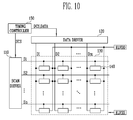
- FIG. 10 is a schematic view showing an organic light emitting display according to one embodiment of the present invention.
- Referring to FIG. 10, the organic light emitting display according to the embodiment of the present invention includes a
pixel unit 130 includingpixels 140 formed in an intersection region of scan lines (S1 to Sn) and data lines (D1 to Dm); ascan driver 110 for driving the scan lines (S 1 to Sn); adata driver 120 for driving the data lines (D1 to Dm); and atiming controller 150 for controlling thescan driver 110 and thedata driver 120. - The
data driver 120 generates data signals in response to a data driving control signal (DCS) supplied from atiming controller 150, and supplies the generated data signals to the data lines (D1 to Dm). At this time, thedata driver 120 supplies the data signals, corresponding to one line, to the data lines (D1 to Dm) in every horizontal period (1H). - The
scan driver 110 generates scan signals in response to a scan driving control signal (SCS) (for example, a driving waveform as shown in FIG. 7) supplied from thetiming controller 150, and supplies the generated scan signals to the scan lines (S 1 to Sn). Here, the scan signals generated in thescan driver 110 are randomly or sequentially supplied to the scan lines (S1 to Sn). And, thescan driver 110 is composed of OR gates composed of PMOS transistor, and then formed in a panel. - Meanwhile, in order to reduce a mounting area of a panel,
decoders scan driver 110 may be formed on thedata driver 120 in a form of an integrated circuit. That is to say, adata driver 120 is formed to include thedecoders data driver 120 is formed. And, ascan driver 110 may be stably driven by electronically connecting thedecoders - The
timing controller 150 generates a data driving control signal (DCS) and a scan driving control signal (SCS) to correspond to synchronizing signals supplied from the outside. The data driving control signals (DCS) generated in thetiming controller 150 are supplied to thedata driver 120, and the scan driving control signals (SCS) is supplied to thescan driver 110. And, thetiming controller 150 rearranges datas supplied from the outside, and supplies the datas to thedata driver 120. - The
pixel unit 130 receives a first driving power source (ELVDD) and a second driving power source (ELVSS) from the outside, and supplies the first driving power source (ELVDD) and the second driving power source (ELVSS) to each of thepixels 140. Thepixels 140 receiving the first driving power source (ELVDD) and the second driving power source (ELVSS) correspond to the data signal, thereby to control an electric current capacity flowing from the first driving power source (ELVDD) to the second driving power source (ELVSS) via an organic light emitting diode. For this purpose, each of thepixels 140 includes at least one transistor. Here, the transistors included in each of thepixels 140 are formed along with the transistors included in thescan driver 110 as PMOS transistors. - As described above, the logic gate according to the embodiment of the present invention, and the scan driver and the organic light emitting display using the same may be useful to constitute the scan driver using the OR gates composed of PMOS transistors. In this case, it is possible to mount a scan driver in a panel without increase of the number of masks since all transistors in the scan driver are PMOS transistors. Therefore, the manufacturing cost may be reduced. Also, the scan driver of the present invention may variously set up the order of the scan signals supplied to the scan lines by varying the connection between the driving waveform and/or the OR gates, therefore the scan driver may be easily applicable to various driving processes.
- The description proposed herein is just a preferable example for the purpose of illustrations only, not intended to limit the scope of the invention, so it should be understood that other equivalents and modifications could be made thereto without departing from the spirit and scope of the invention as apparent to those skilled in the art. Therefore, it should be understood that the present invention might be not defined within the scope of which is described in detailed description but within the scope of which is defined in the claims and their equivalents.
Claims (18)
wherein the second driver is adapted to provide the second power supply voltage to the first node when the first driver does not provide the first power supply voltage to the first node;
wherein the third driver is adapted to provide the first power supply voltage to the output terminal when the second power supply voltage is provided to the first node; and
wherein the fourth driver is adapted to provide the second power supply voltage to the gate electrode of the control transistor when the third driver does not provide the first power supply voltage to the output terminal,
wherein each of the first driver, the second driver, the third driver and the fourth driver comprises at least one transistor (M1, M2, M3, M4, M5, M6, M7, M9, M10, M11, M20, M21, M22, M23, M24, M25, M30, M31, M32, M33), and the transistors and the control transistor are MOS transistors of the same polarity type.
a third plurality of transistors (M23, M24, M25) connected in parallel between the gate electrode of the fourth transistor and the second terminal of the second driver, wherein each of the third plurality of transistors comprises a gate electrode connected to a corresponding one of a plurality of input bar terminals adapted to received a plurality of inverted input signals (/IN1, /IN2, /IN3).
wherein a width/length ratio of the control transistor is set to a narrower range than that of the sixth transistor.
Applications Claiming Priority (1)
| Application Number | Priority Date | Filing Date | Title |
|---|---|---|---|
| KR1020060074586A KR100748360B1 (en) | 2006-08-08 | 2006-08-08 | Logic gate, scan driver and organic light emitting display using the same |
Publications (3)
| Publication Number | Publication Date |
|---|---|
| EP1912332A2 true EP1912332A2 (en) | 2008-04-16 |
| EP1912332A3 EP1912332A3 (en) | 2008-05-21 |
| EP1912332B1 EP1912332B1 (en) | 2012-04-18 |
Family
ID=38511399
Family Applications (1)
| Application Number | Title | Priority Date | Filing Date |
|---|---|---|---|
| EP07114023A Active EP1912332B1 (en) | 2006-08-08 | 2007-08-08 | Logic gate, scan driver and organic light emitting diode display using the same |
Country Status (5)
| Country | Link |
|---|---|
| US (1) | US7528631B2 (en) |
| EP (1) | EP1912332B1 (en) |
| JP (2) | JP4891725B2 (en) |
| KR (1) | KR100748360B1 (en) |
| CN (1) | CN101227188B (en) |
Families Citing this family (7)
| Publication number | Priority date | Publication date | Assignee | Title |
|---|---|---|---|---|
| KR101581401B1 (en) | 2009-11-06 | 2015-12-31 | 삼성디스플레이 주식회사 | Apparatus for scan driving |
| KR101107163B1 (en) | 2010-05-25 | 2012-01-25 | 삼성모바일디스플레이주식회사 | Scan driver and display device using the same |
| KR101990568B1 (en) | 2013-07-24 | 2019-06-19 | 삼성디스플레이 주식회사 | Scan driver and organic emmiting display device using the same |
| KR102412674B1 (en) * | 2015-09-21 | 2022-06-24 | 삼성디스플레이 주식회사 | Scan driver and display device including the same |
| CN105913818B (en) * | 2016-06-07 | 2018-06-29 | 深圳市华星光电技术有限公司 | The scan compensation method of gate drivers and scan compensation circuit |
| CN106328040B (en) * | 2016-10-31 | 2019-06-28 | 昆山国显光电有限公司 | GIP circuit and its driving method and panel display apparatus |
| CN112259038B (en) * | 2020-11-16 | 2023-07-14 | 武汉天马微电子有限公司 | Shift register and driving method, grid driving circuit, display panel and device |
Citations (1)
| Publication number | Priority date | Publication date | Assignee | Title |
|---|---|---|---|---|
| US5694061A (en) | 1995-03-27 | 1997-12-02 | Casio Computer Co., Ltd. | Semiconductor device having same conductive type MIS transistors, a simple circuit design, and a high productivity |
Family Cites Families (16)
| Publication number | Priority date | Publication date | Assignee | Title |
|---|---|---|---|---|
| JPS4931243U (en) * | 1972-06-17 | 1974-03-18 | ||
| JPS5318129B2 (en) * | 1972-07-21 | 1978-06-13 | ||
| JPS50128971A (en) * | 1974-03-29 | 1975-10-11 | ||
| US4709724A (en) | 1986-01-17 | 1987-12-01 | Commercial Shearing, Inc. | Fluid valve structures |
| JP3036910B2 (en) | 1991-08-20 | 2000-04-24 | 沖電気工業株式会社 | CMOS decode circuit |
| JP3005730B2 (en) * | 1991-10-01 | 2000-02-07 | 日本電気エンジニアリング株式会社 | OR circuit |
| JPH05300007A (en) * | 1992-04-16 | 1993-11-12 | Nippon Steel Corp | Two-input or circuit |
| US5517133A (en) * | 1993-07-14 | 1996-05-14 | Sun Microsystems, Inc. | Multiple-input OR-gate employing a sense amplifier |
| KR970000888B1 (en) | 1994-05-28 | 1997-01-21 | 대우자동차 주식회사 | Rock cylinder fixing device for automobile trunk |
| JPH0832441A (en) | 1994-07-14 | 1996-02-02 | Hitachi Ltd | Logic circuit and decoder using this circuit |
| KR100197188B1 (en) * | 1995-04-17 | 1999-06-15 | 모리시다 요이치 | Voltage level converting circuit |
| KR0182028B1 (en) * | 1995-07-18 | 1999-04-15 | 김광호 | Logic gate circuit using mos-transistor |
| KR100314732B1 (en) * | 1998-09-28 | 2002-01-17 | 박종섭 | Sate machine using the OR gate circuit |
| CN1214531C (en) * | 1999-10-15 | 2005-08-10 | 威盛电子股份有限公司 | Single-terminal input voltage level converter controlled by grid voltage |
| KR100490623B1 (en) * | 2003-02-24 | 2005-05-17 | 삼성에스디아이 주식회사 | Buffer circuit and active matrix display device using the same |
| US7623097B2 (en) * | 2005-08-17 | 2009-11-24 | Samsung Mobile Display Co., Ltd. | Emission control driver and organic light emitting display device having the same and a logical or circuit for an emission control driver for outputting an emission control signal |
-
2006
- 2006-08-08 KR KR1020060074586A patent/KR100748360B1/en active IP Right Grant
- 2006-10-05 JP JP2006274364A patent/JP4891725B2/en active Active
-
2007
- 2007-07-13 US US11/826,321 patent/US7528631B2/en active Active
- 2007-08-08 EP EP07114023A patent/EP1912332B1/en active Active
- 2007-08-08 CN CN2007101596040A patent/CN101227188B/en active Active
-
2010
- 2010-10-12 JP JP2010229932A patent/JP5604254B2/en active Active
Patent Citations (1)
| Publication number | Priority date | Publication date | Assignee | Title |
|---|---|---|---|---|
| US5694061A (en) | 1995-03-27 | 1997-12-02 | Casio Computer Co., Ltd. | Semiconductor device having same conductive type MIS transistors, a simple circuit design, and a high productivity |
Also Published As
| Publication number | Publication date |
|---|---|
| JP2011059697A (en) | 2011-03-24 |
| JP2008040445A (en) | 2008-02-21 |
| EP1912332B1 (en) | 2012-04-18 |
| US20080036497A1 (en) | 2008-02-14 |
| CN101227188B (en) | 2011-04-06 |
| CN101227188A (en) | 2008-07-23 |
| JP5604254B2 (en) | 2014-10-08 |
| US7528631B2 (en) | 2009-05-05 |
| JP4891725B2 (en) | 2012-03-07 |
| EP1912332A3 (en) | 2008-05-21 |
| KR100748360B1 (en) | 2007-08-09 |
Similar Documents
| Publication | Publication Date | Title |
|---|---|---|
| EP1763003B1 (en) | Emission control line driver and organic light emitting display using the emission control line driver | |
| US9443464B2 (en) | Stage circuit and organic light emitting display device using the same | |
| US8599117B2 (en) | Emission control driver and organic light emitting display device using the same | |
| EP1912332B1 (en) | Logic gate, scan driver and organic light emitting diode display using the same | |
| US8963906B2 (en) | Display device using a charge sharing unit and method for driving the same | |
| US7847760B2 (en) | Pixel circuit, organic light emitting display using the pixel circuit and driving method for the display | |
| US8665182B2 (en) | Emission control driver and organic light emitting display device using the same | |
| US8290115B2 (en) | Driver and organic light emitting diode display using the same | |
| US9019191B2 (en) | Stage circuit and emission control driver using the same | |
| US7808471B2 (en) | Scan driving circuit and organic light emitting display using the same | |
| KR20070057410A (en) | A shift register | |
| JP2007034305A (en) | Display device | |
| KR20080111233A (en) | Driving apparatus for liquid crystal display and liquid crystal display including the same | |
| US9099040B2 (en) | Scan driver and organic light emitting display using the same | |
| WO2015163305A1 (en) | Active matrix substrate and display device provided with same | |
| US7304622B2 (en) | Gate driver for an active matrix liquid crystal display device | |
| KR100748359B1 (en) | Logic gate, scan driver and organic light emitting display using the same | |
| WO2015163306A1 (en) | Active-matrix substrate and display device provided with same | |
| US7535260B2 (en) | Logic gates, scan drivers and organic light emitting displays using the same | |
| KR102015848B1 (en) | Liquid crystal display device | |
| KR20190018932A (en) | Gate driver and organic light emitting display device including the same | |
| KR102138664B1 (en) | Display device | |
| KR100748361B1 (en) | Logic gate, scan driver and organic light emitting display using the same | |
| KR100805566B1 (en) | Buffer and organic light emitting display using the buffer | |
| US7893893B2 (en) | Driving arrangement for an OLED panel |
Legal Events
| Date | Code | Title | Description |
|---|---|---|---|
| PUAI | Public reference made under article 153(3) epc to a published international application that has entered the european phase |
Free format text: ORIGINAL CODE: 0009012 |
|
| 17P | Request for examination filed |
Effective date: 20070808 |
|
| AK | Designated contracting states |
Kind code of ref document: A2 Designated state(s): AT BE BG CH CY CZ DE DK EE ES FI FR GB GR HU IE IS IT LI LT LU LV MC MT NL PL PT RO SE SI SK TR |
|
| AX | Request for extension of the european patent |
Extension state: AL BA HR MK RS |
|
| PUAL | Search report despatched |
Free format text: ORIGINAL CODE: 0009013 |
|
| AK | Designated contracting states |
Kind code of ref document: A3 Designated state(s): AT BE BG CH CY CZ DE DK EE ES FI FR GB GR HU IE IS IT LI LT LU LV MC MT NL PL PT RO SE SI SK TR |
|
| AX | Request for extension of the european patent |
Extension state: AL BA HR MK RS |
|
| AKX | Designation fees paid |
Designated state(s): DE FR GB HU |
|
| RAP1 | Party data changed (applicant data changed or rights of an application transferred) |
Owner name: SAMSUNG MOBILE DISPLAY CO., LTD. |
|
| 17Q | First examination report despatched |
Effective date: 20090924 |
|
| GRAP | Despatch of communication of intention to grant a patent |
Free format text: ORIGINAL CODE: EPIDOSNIGR1 |
|
| GRAS | Grant fee paid |
Free format text: ORIGINAL CODE: EPIDOSNIGR3 |
|
| GRAA | (expected) grant |
Free format text: ORIGINAL CODE: 0009210 |
|
| AK | Designated contracting states |
Kind code of ref document: B1 Designated state(s): DE FR GB HU |
|
| REG | Reference to a national code |
Ref country code: GB Ref legal event code: FG4D |
|
| REG | Reference to a national code |
Ref country code: DE Ref legal event code: R096 Ref document number: 602007022063 Country of ref document: DE Effective date: 20120614 |
|
| REG | Reference to a national code |
Ref country code: GB Ref legal event code: 732E Free format text: REGISTERED BETWEEN 20130103 AND 20130109 |
|
| PLBE | No opposition filed within time limit |
Free format text: ORIGINAL CODE: 0009261 |
|
| STAA | Information on the status of an ep patent application or granted ep patent |
Free format text: STATUS: NO OPPOSITION FILED WITHIN TIME LIMIT |
|
| 26N | No opposition filed |
Effective date: 20130121 |
|
| REG | Reference to a national code |
Ref country code: DE Ref legal event code: R082 Ref document number: 602007022063 Country of ref document: DE Representative=s name: GULDE HENGELHAUPT ZIEBIG & SCHNEIDER, DE |
|
| REG | Reference to a national code |
Ref country code: DE Ref legal event code: R097 Ref document number: 602007022063 Country of ref document: DE Effective date: 20130121 |
|
| REG | Reference to a national code |
Ref country code: DE Ref legal event code: R081 Ref document number: 602007022063 Country of ref document: DE Owner name: SAMSUNG DISPLAY CO., LTD., KR Free format text: FORMER OWNER: SAMSUNG MOBILE DISPLAY CO., LTD., SUWON-SI, KR Effective date: 20130416 Ref country code: DE Ref legal event code: R082 Ref document number: 602007022063 Country of ref document: DE Representative=s name: GULDE HENGELHAUPT ZIEBIG & SCHNEIDER, DE Effective date: 20130416 Ref country code: DE Ref legal event code: R082 Ref document number: 602007022063 Country of ref document: DE Representative=s name: GULDE & PARTNER PATENT- UND RECHTSANWALTSKANZL, DE Effective date: 20130416 Ref country code: DE Ref legal event code: R081 Ref document number: 602007022063 Country of ref document: DE Owner name: SAMSUNG DISPLAY CO., LTD., YONGIN-CITY, KR Free format text: FORMER OWNER: SAMSUNG MOBILE DISPLAY CO., LTD., SUWON-SI, KYONGGI-DO, KR Effective date: 20130416 |
|
| PG25 | Lapsed in a contracting state [announced via postgrant information from national office to epo] |
Ref country code: HU Free format text: LAPSE BECAUSE OF FAILURE TO SUBMIT A TRANSLATION OF THE DESCRIPTION OR TO PAY THE FEE WITHIN THE PRESCRIBED TIME-LIMIT Effective date: 20070808 |
|
| REG | Reference to a national code |
Ref country code: FR Ref legal event code: PLFP Year of fee payment: 10 |
|
| REG | Reference to a national code |
Ref country code: FR Ref legal event code: PLFP Year of fee payment: 11 |
|
| REG | Reference to a national code |
Ref country code: FR Ref legal event code: PLFP Year of fee payment: 12 |
|
| P01 | Opt-out of the competence of the unified patent court (upc) registered |
Effective date: 20230515 |
|
| PGFP | Annual fee paid to national office [announced via postgrant information from national office to epo] |
Ref country code: GB Payment date: 20230720 Year of fee payment: 17 |
|
| PGFP | Annual fee paid to national office [announced via postgrant information from national office to epo] |
Ref country code: FR Payment date: 20230725 Year of fee payment: 17 Ref country code: DE Payment date: 20230720 Year of fee payment: 17 |