EP1911094B1 - Radiation detecting apparatus and radiation detecting system - Google Patents
Radiation detecting apparatus and radiation detecting system Download PDFInfo
- Publication number
- EP1911094B1 EP1911094B1 EP06768394.6A EP06768394A EP1911094B1 EP 1911094 B1 EP1911094 B1 EP 1911094B1 EP 06768394 A EP06768394 A EP 06768394A EP 1911094 B1 EP1911094 B1 EP 1911094B1
- Authority
- EP
- European Patent Office
- Prior art keywords
- electrode
- conversion element
- wiring
- disposed
- switching element
- Prior art date
- Legal status (The legal status is an assumption and is not a legal conclusion. Google has not performed a legal analysis and makes no representation as to the accuracy of the status listed.)
- Not-in-force
Links
- 230000005855 radiation Effects 0.000 title claims description 97
- 238000006243 chemical reaction Methods 0.000 claims description 189
- 239000000758 substrate Substances 0.000 claims description 44
- 238000009413 insulation Methods 0.000 claims description 38
- 239000011159 matrix material Substances 0.000 claims description 14
- 238000000034 method Methods 0.000 claims description 3
- 230000005540 biological transmission Effects 0.000 claims description 2
- 239000011347 resin Substances 0.000 claims 1
- 229920005989 resin Polymers 0.000 claims 1
- 239000010410 layer Substances 0.000 description 166
- 239000004065 semiconductor Substances 0.000 description 45
- OAICVXFJPJFONN-UHFFFAOYSA-N Phosphorus Chemical compound [P] OAICVXFJPJFONN-UHFFFAOYSA-N 0.000 description 34
- 239000000463 material Substances 0.000 description 18
- 238000004519 manufacturing process Methods 0.000 description 17
- 239000011669 selenium Substances 0.000 description 13
- 239000010408 film Substances 0.000 description 9
- 230000005260 alpha ray Effects 0.000 description 8
- 230000005250 beta ray Effects 0.000 description 8
- 230000005251 gamma ray Effects 0.000 description 8
- BUGBHKTXTAQXES-UHFFFAOYSA-N Selenium Chemical compound [Se] BUGBHKTXTAQXES-UHFFFAOYSA-N 0.000 description 7
- 239000011229 interlayer Substances 0.000 description 7
- 229910052711 selenium Inorganic materials 0.000 description 7
- 239000010409 thin film Substances 0.000 description 7
- 238000010586 diagram Methods 0.000 description 6
- OKTJSMMVPCPJKN-UHFFFAOYSA-N Carbon Chemical compound [C] OKTJSMMVPCPJKN-UHFFFAOYSA-N 0.000 description 5
- 239000000853 adhesive Substances 0.000 description 5
- 230000001070 adhesive effect Effects 0.000 description 5
- 229910052799 carbon Inorganic materials 0.000 description 5
- 238000000151 deposition Methods 0.000 description 5
- 230000002093 peripheral effect Effects 0.000 description 5
- 230000000087 stabilizing effect Effects 0.000 description 5
- 238000006073 displacement reaction Methods 0.000 description 4
- 230000001965 increasing effect Effects 0.000 description 4
- 230000007423 decrease Effects 0.000 description 3
- 230000000694 effects Effects 0.000 description 3
- 239000004925 Acrylic resin Substances 0.000 description 2
- 229920000178 Acrylic resin Polymers 0.000 description 2
- 239000004642 Polyimide Substances 0.000 description 2
- UMIVXZPTRXBADB-UHFFFAOYSA-N benzocyclobutene Chemical compound C1=CC=C2CCC2=C1 UMIVXZPTRXBADB-UHFFFAOYSA-N 0.000 description 2
- 230000000903 blocking effect Effects 0.000 description 2
- 239000000969 carrier Substances 0.000 description 2
- 238000002955 isolation Methods 0.000 description 2
- 230000003287 optical effect Effects 0.000 description 2
- 229920001721 polyimide Polymers 0.000 description 2
- 239000012780 transparent material Substances 0.000 description 2
- 230000015572 biosynthetic process Effects 0.000 description 1
- 230000003247 decreasing effect Effects 0.000 description 1
- 238000001514 detection method Methods 0.000 description 1
- 238000003745 diagnosis Methods 0.000 description 1
- 230000001939 inductive effect Effects 0.000 description 1
- 238000007689 inspection Methods 0.000 description 1
- 239000002184 metal Substances 0.000 description 1
- 238000002360 preparation method Methods 0.000 description 1
- 230000000452 restraining effect Effects 0.000 description 1
- 230000035945 sensitivity Effects 0.000 description 1
- 239000000126 substance Substances 0.000 description 1
Images


Classifications
-
- H—ELECTRICITY
- H01—ELECTRIC ELEMENTS
- H01L—SEMICONDUCTOR DEVICES NOT COVERED BY CLASS H10
- H01L27/00—Devices consisting of a plurality of semiconductor or other solid-state components formed in or on a common substrate
- H01L27/14—Devices consisting of a plurality of semiconductor or other solid-state components formed in or on a common substrate including semiconductor components sensitive to infrared radiation, light, electromagnetic radiation of shorter wavelength or corpuscular radiation and specially adapted either for the conversion of the energy of such radiation into electrical energy or for the control of electrical energy by such radiation
- H01L27/144—Devices controlled by radiation
- H01L27/146—Imager structures
- H01L27/14643—Photodiode arrays; MOS imagers
- H01L27/14658—X-ray, gamma-ray or corpuscular radiation imagers
- H01L27/14663—Indirect radiation imagers, e.g. using luminescent members
-
- H—ELECTRICITY
- H01—ELECTRIC ELEMENTS
- H01L—SEMICONDUCTOR DEVICES NOT COVERED BY CLASS H10
- H01L31/00—Semiconductor devices sensitive to infrared radiation, light, electromagnetic radiation of shorter wavelength or corpuscular radiation and specially adapted either for the conversion of the energy of such radiation into electrical energy or for the control of electrical energy by such radiation; Processes or apparatus specially adapted for the manufacture or treatment thereof or of parts thereof; Details thereof
- H01L31/08—Semiconductor devices sensitive to infrared radiation, light, electromagnetic radiation of shorter wavelength or corpuscular radiation and specially adapted either for the conversion of the energy of such radiation into electrical energy or for the control of electrical energy by such radiation; Processes or apparatus specially adapted for the manufacture or treatment thereof or of parts thereof; Details thereof in which radiation controls flow of current through the device, e.g. photoresistors
- H01L31/10—Semiconductor devices sensitive to infrared radiation, light, electromagnetic radiation of shorter wavelength or corpuscular radiation and specially adapted either for the conversion of the energy of such radiation into electrical energy or for the control of electrical energy by such radiation; Processes or apparatus specially adapted for the manufacture or treatment thereof or of parts thereof; Details thereof in which radiation controls flow of current through the device, e.g. photoresistors characterised by at least one potential-jump barrier or surface barrier, e.g. phototransistors
- H01L31/115—Devices sensitive to very short wavelength, e.g. X-rays, gamma-rays or corpuscular radiation
- H01L31/119—Devices sensitive to very short wavelength, e.g. X-rays, gamma-rays or corpuscular radiation characterised by field-effect operation, e.g. MIS type detectors
Definitions
- the present invention relates to a radiation detecting apparatus for converting a radiation into an electrical signal, and to a radiation detecting system utilizing such radiation detecting apparatus.
- the conversion element includes, for example, following two types.
- One is an indirect type conversion element constituted of a photoelectric conversion element and a wavelength conversion member (such as a phosphor) for converting a radiation such as an X-ray into a light of a wavelength region detectable by the photoelectric conversion element.
- Such indirect type conversion element executes a wavelength conversion of the radiation such as X-ray into a light, by means of a wavelength conversion member such as a phosphor, disposed on a photoelectric conversion element, and executes a photoelectric conversion on the light from the wavelength conversion member by the photoelectric conversion element.
- the other is a direct type conversion element which directly converts the radiation such as an X-ray into an electrical signal, by means of a direct conversion semiconductor element including a semiconductor conversion material, capable of converting the radiation such as an X-ray into the electrical signal, such as amorphous selenium (a-Se).
- the conversion element includes at least an upper electrode, a lower electrode and a semiconductor layer for converting the radiation into the electrical signal or a semiconductor layer for converting the light into the electrical signal, disposed between the upper and lower electrodes, and either one of the electrodes is two-dimensionally divided for pixel isolation, thereby realizing a two-dimensional array of pixels.
- U.S. Patent No. 6,020,590 describes disposing a conversion element part, including a direct conversion semiconductor element, on a switching element part containing the switching element such as TFT.
- a conversion element part photoelectric conversion element
- a phosphor is further disposed thereon ( Fig. 20 ).
- the pixel electrode of the conversion element part is divided on the signal wiring, connected to the source electrode or the drain electrode of the TFT constituting the switching element part, and on the gate wiring.
- the document JP 2004 265935 A discloses a prior radiation detecting apparatus, which aims at restraining a thin film transistor from varying in threshold voltage so as to keep it stable in TFT characteristics in a structure where a part or all of the thin film transistor is covered with a photoelectric conversion element.
- a photodetector and one or more thin film transistors connected to the photodetector are formed in a pixel.
- the photodetector is stacked up on the thin film transistors overlapping, at least, partially with them.
- the thin film transistor is composed of a source electrode, a drain electrode, a first gate electrode, and a second gate electrode which is arranged on a side opposite to the first gate electrode to the source electrode and the drain electrode, and the first gate electrode is connected to the second gate electrode in each pixel.
- the document WO 2004 73068 shows a radiation image pickup device having different types of pixel layouts.
- An object of the present invention is to provide a radiation detecting apparatus and a radiation detecting system utilizing such radiation detecting apparatus, capable of realizing a higher definition in a captured image, and having a more easily manufacturable structure.
- arranged in one direction or “arranged in a direction different from the aforementioned one direction” means not only an arrangement in a linear array but also includes a case where a switching element is disposed on both sides on a wiring, as in a case of gate wiring shown in Fig. 18 .
- the conversion element for converting a radiation into an electrical signal means an element capable of receiving a radiation such as a visible light, an infrared light, an X-ray, an ⁇ -ray, a ⁇ -ray or a ⁇ -ray and converting it into an electrical signal, and includes a photoelectric conversion element for converting a light such as a visible light or an infrared light into an electrical signal, and an element including for example amorphous selenium as a semiconductor layer and capable of converting a radiation such as an X-ray into an electrical signal.
- the present invention allows to reduce and stabilize a variation in a capacity between a wiring connected with the switching element and an electrode of the conversion element, thereby providing a radiation detecting apparatus of stabilized characteristics. And capable of providing a captured image or a displayed image for example with suppressed artifacts.
- the present invention allows to dispense with a strict alignment between a wiring connected with the switching element and an electrode of the conversion element and also allows a manufacture with a reduced influence of a step difference caused by wirings, thereby facilitating the manufacturing process.
- the radiation detecting apparatus of the present invention will be explained in detail by an example of a radiation detecting apparatus for converting a radiation such as an X-ray into an electrical signal. But it is not limited to such radiation detecting apparatus but is applicable also to a detecting apparatus which converts a light, such as a visible light or an infrared light, into an electrical signal.
- the present example has a structure in which a signal wiring or a gate wiring, constituting a control wiring, passes under a pixel electrode, isolated for each pixel, of a conversion element constituted of a photoelectric conversion element.
- Figs. 1 and 2 illustrate a case in which the signal wiring is disposed under the pixel electrode.
- Fig. 1 is a plan view showing a structure of a pixel in the radiation detecting apparatus of the first example, illustrating a pixel including a switching element formed by a TFT and a conversion element and to be disposed in a two-dimensional matrix array.
- Fig. 2 is a cross-sectional view along a line 2-2 in Fig. 1 .
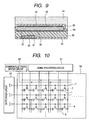
- Figs. 10 and 11 are respectively an equivalent circuit diagram and a perspective view of a radiation detecting apparatus, in which the pixel shown in Figs. 1 and 2 is arranged in a matrix array.
- a conversion element 1 is constituted of an MIS photoelectric conversion element of a metal-insulator-semiconductor structure for converting a light, such as a visible light or an infrared light, into an electrical signal.
- a phosphor (not shown in Fig. 1 ) is disposed thereon as a wavelength converting member for converting a radiation such as an X-ray, an ⁇ -ray a ⁇ -ray or a ⁇ -ray into a light, such as a visible light, that can be photoelectrically converted in the MIS photoelectric conversion element.
- the phosphor may be constituted, for example, of CsI which converts an X-ray into a light.
- a switching element 2 constituted of a TFT (thin film transistor) and functioning as a switching element, has three electrodes, including a source electrode 3 and a drain electrode 4 as two terminals, and a gate electrode 5 serving as a control terminal.
- a channel of the switching element 2 exists between the source electrode 3 and the drain electrode 4, and a charge flow in the channel can be controlled by a voltage control on the gate electrode 5.
- the conversion element 1 has a layered structure from a pixel electrode 9 isolated for each pixel to a region under the bias wiring 8, and is disposed on the switching element 2.
- the pixel electrode 9 of the conversion element 1 is connected, via a through hole 10, to the drain electrode 4 of the switching element 2.
- Fig. 2 showing a cross-sectional view along a line 2-2 in Fig. 1 , for explaining the layered structure of a pixel in the first example.
- the switching element 2 is disposed on a substrate, then the conversion element 1 is disposed thereon, and a phosphor layer 44 is disposed further thereon.
- the switching element 2 includes a first electrode layer 31 constituting a gate electrode (corresponding to the gate electrode 5 in Fig. 1 ) and a gate wiring (corresponding to the gate wiring 7 in Fig. 1 ), a first insulation layer 32 constituting a gate insulation film, a first semiconductor layer 33, a first impurity-doped semiconductor layer 34 constituting an ohmic contact layer, and a second electrode layer 35 constituting source and drain electrodes (corresponding to the source electrode 3 and the drain electrode 4 in Fig. 1 ) and a signal wiring (corresponding the signal wiring 6 in Fig. 1 ).
- the conversion element 1 is an MIS photoelectric converting element including a third electrode layer 37 isolated for each pixel (corresponding to the pixel electrode 9 in Fig. 1 ), a third insulation layer 38, a second semiconductor layer 39, a second impurity-doped semiconductor layer 40 functioning as an ohmic contact layer or a blocking layer, and a fifth electrode layer 42 (constituting an upper electrode), and is capable of a photoelectric conversion on a light such as a visible light.
- a fifth electrode layer 42 constituted of a transparent material such as ITO is disposed on the second impurity-doped semiconductor layer 40, but, in the case that the second impurity-doped semiconductor layer 40 has a low resistance, it may also serve as the electrode layer and the fifth electrode layer 42 may be dispensed with. In such case, the second impurity-doped semiconductor layer 40 serves as an upper electrode of the conversion element 1.
- a fourth electrode layer 41 is a bias wiring (corresponding to a bias wiring 8 in Fig. 1 ) for a voltage application to the fifth electrode layer 42, and is connected to a common electrode driver circuit (common electrode driver circuit 53 in Fig. 10 ).
- the fourth electrode layer 41 is covered by the fifth electrode layer 42, but it is also possible to dispose the fifth electrode layer 42 under the fourth electrode layer 41.
- the third electrode layer 37 (corresponding to the pixel electrode 9 in Fig. 1 ) of the conversion element 1 is connected to one of the electrodes (drain electrode) formed by the second electrode layer 35 constituting the switching element 2, via a through hole (corresponding to the through hole 10 in Fig. 1 ) formed in the second insulation layer 36 constituting the interlayer insulation layer.
- a charge corresponding to the carriers generated in the second semiconductor layer 39 of the conversion element 1 can be transferred to an external signal processing circuit (signal processing circuit 51 shown in Fig. 10 ).
- the signal wiring 6 is so disposed as to pass through such area in such a manner that both ends thereof opposite to each other in a width direction are present in such area (passing through under the pixel electrode 9 of the conversion element 1 without jetting out).
- a similar effect can be obtained by disposing the gate wiring 7, in an area between a normal projection area of the pixel electrode 9 on the substrate and the pixel electrode 9, so as to pass through such area in such a manner that both ends opposite to each other in a width direction are present in such area (so as to be inside the electrode area when seen from above the conversion element, or so as that the gate electrode 7 passes through under the pixel electrode 9 of the conversion element 1 without jetting out). It is therefore also possible to dispose the gate wiring 7 alone so as to pass through inside such area.
- a similar effect can be obtained by disposing the switching element 2 within an area between a normal projection area of the pixel electrode 9 on the substrate and the pixel electrode 9.
- a part of the source electrode 3 or the drain electrode 4 of the switching element 2 protrudes out from under the pixel electrode 9 and is disposed in an adjacent pixel area
- a variation of the capacitance among the pixels is caused by a displaced positional relationship, induced by an alignment error in the exposure apparatus employed in the manufacturing process.
- Fig. 21 schematically shows a state in which a signal wiring 6 or a gate wiring 7 passes through an area 101 between a normal projection area 102 of the pixel electrode 9 onto the substrate 100 and the pixel electrode 9.
- the third electrode layer 37 (pixel electrode of the conversion element 1) is so disposed as to cover the second electrode layer 35 constituting the signal wiring 6.
- the signal wiring 6 is so disposed as to pass through such area in such a manner that both ends thereof opposite to each other in a width direction are present in such area. Therefore, even in case of an alignment error in the exposure apparatus employed in the manufacturing process, the overlapping area remains constant to suppress a capacitance variation in the pixel electrode 9.
- the fifth electrode layer 42 (upper electrode of the conversion element 1) is preferably so disposed as to cover the second electrode layer 35, constituting the signal wiring 6.
- both the third electrode layer 37 (pixel electrode of the conversion element 1) and the fifth electrode layer 42 (upper electrode of the conversion element 1) are so disposed as to cover the second electrode layer 35 constituting the signal wiring 6.
- the third electrode layer 37 (pixel electrode of the conversion element 1) is so constructed as to cover the gate wiring 7
- the fifth electrode layer 42 (upper electrode of the conversion element 1) is also so disposed as to cover the gate wiring 7.
- the third electrode layer 37 (pixel electrode of the conversion element 1) is so constructed as to cover the switching element 2
- the fifth electrode layer 42 (upper electrode of the conversion element 1) is also so disposed as to cover the switching element 2.
- Figs. 10 and 11 for explaining a constitution of a radiation detecting apparatus, formed by disposing the pixels, explained in Figs. 1 and 2 , in a matrix array.
- pixels each having a conversion element 1 and a switching element 2 are arrayed in a two-dimensional matrix on a substrate.
- gate wirings 7 connected to the gate electrodes 5 of the switching elements 2 and signal wirings 6 connected to the source electrodes 3 of the switching elements 2 are provided respectively by a number corresponding a number of rows of the pixels and by a number corresponding to a number of columns of the pixels.
- a signal processing circuit 51, a common electrode driver circuit 52 and a gate driver circuit 52 are disposed in a peripheral portion of the substrate.
- the gate driver circuit 52 and the signal processing circuit 51 are disposed in a peripheral portion of a panel, and a phosphor is disposed thereon, for converting a radiation into a light such as a visible light.
- Fig. 10 shows the signal processing circuit 51 and the common electrode driver circuit 53 separately, but in fact the common electrode driver circuit 53 is incorporated in the signal processing circuit 51 as shown in Fig. 11 .
- the gate driver circuit 52 and the signal processing circuit 51 are connected to the substrate 50 through a TCP (tape carrier package: a film carrying an IC) carrying an IC.
- TCP tape carrier package: a film carrying an IC
- the semiconductor element capable of direct conversion of X-ray may include a semiconductor material such as amorphous selenium (a-Se).
- a-Se amorphous selenium
- the present example shows a case in which a signal wiring and a gate wiring pass through under a pixel electrode.
- Fig. 3 is a plan view showing a structure of a pixel in the second example useful for understanding the present invention
- Fig. 4 is a cross-sectional view along a line 4-4 in Fig. 3
- Fig. 5 is a cross-sectional view along a line 5-5 in Fig. 3 .
- components same as or equivalent to those in Fig. 2 are represented by like characters and not explained further.
- the constitution of the radiation detecting apparatus formed by a two-dimensional matrix array of pixels is same as that in Figs. 10 and 11 .
- a conversion element 1 is constituted, as in the example 1, of an MIS photoelectric conversion element.
- a phosphor such as CsI is disposed as a wavelength converting member for converting a radiation such as an X-ray, an ⁇ -ray a ⁇ -ray or a ⁇ -ray into a light, such as a visible light, that can be photoelectrically converted in the MIS photoelectric conversion element.
- the signal wiring 6 is so disposed, in the area between the normal projection area of the pixel electrode 9 on the substrate and the pixel electrode 9, as to pass through such area in such a manner that both ends opposite to each other in a width direction are present in such area (so as to be inside the electrode area without jetting out).
- the present example shown in Fig. 3 not only the signal wiring 6 but also the gate wiring 7 are so disposed as to pass through the aforementioned area in such a manner that both ends opposite to each other in a width direction are present in such area.
- the third electrode layer 37 (pixel electrode of the conversion element 1) is so disposed as to cover the second electrode layer 35 constituting the signal wiring 6.
- the signal wiring 6 is so disposed as to pass through such area in such a manner that both ends thereof opposite to each other in a width direction are present in such area. Therefore, even in case of an alignment error in the exposure apparatus employed in the manufacturing process, the overlapping area remains constant to suppress a capacitance variation in the pixel electrode 9.
- the fifth electrode layer 42 (upper electrode of the conversion element 1) is preferably so disposed as to cover the second electrode layer 35, constituting the signal wiring 6. And in the present example, both the third electrode layer 37 (pixel electrode of the conversion element 1) and the fifth electrode layer 42 (upper electrode of the conversion element 1) are so disposed as to cover the second electrode layer 35 constituting the signal wiring 6.
- the third electrode layer 37 (pixel electrode of the conversion element 1) is so disposed as to cover the first electrode layer 31 constituting the gate wiring 7.
- the gate wiring 7 is so disposed as to pass through such area in such a manner that both ends of the gate wiring 7 opposite to each other in a width direction are present in such area. Therefore, even in case of an alignment error in the exposure apparatus employed in the manufacturing process, the overlapping area remains constant to suppress a capacitance variation in the pixel electrode 9.
- the fifth electrode layer 42 (upper electrode of the conversion element 1) is preferably so disposed as to cover the first electrode layer 31, constituting the gate wiring 7. And in the present example, both the third electrode layer 37 (pixel electrode of the conversion element 1) and the fifth electrode layer 42 (upper electrode of the conversion element 1) are so disposed as to cover the first electrode layer 31 constituting the gate wiring 7.
- the overlapping area of the signal wiring 6 and the pixel electrode 9 of the conversion element 1 remains same to maintain a constant capacitance between the signal wiring 6 and the pixel electrode 9 of the conversion element 1, whereby image artifacts, resulting from a fluctuation in the capacitance in the pixel, can be suppressed in the image obtained by the radiation detecting apparatus.
- the overlapping area of the gate wiring 7 and the pixel electrode 9 of the conversion element 1 remains constant, even in case of a displacement in the positional relationship by an alignment error, thereby stabilizing the capacitance of the gate wiring 7. Therefore a transfer ability is stabilized among the pixels, and image artifacts, resulting from a fluctuation in the transfer ability among the pixels, can be suppressed.
- the switching element 2 in the area between the normal projection area of the pixel electrode 9 on the substrate and the pixel electrode 9, the overlapping area between the pixel electrode 9 of the conversion element 1 and the switching element 2 remains constant thereby stabilizing the capacitance.
- Figs. 3 to 5 show a system of employing a photoelectric conversion element for converting a light such as a visible light into an electrical signal and depositing a phosphor directly thereon. But it is also possible to form a phosphor on a substrate of a radiation-transmitting material such as carbon and to adhere the surface of such phosphor with an adhesive material to a substrate bearing photoelectric conversion elements. It is also possible to utilize a semiconductor element for converting a radiation such as an X-ray, an ⁇ -ray a ⁇ -ray or a ⁇ -ray directly into an electrical signal as the conversion element 1, thereby dispensing with the phosphor.
- the semiconductor element capable of direct conversion of X-ray may include a semiconductor material such as amorphous selenium (a-Se).
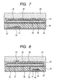
- the present example shows a case in which an organic insulation layer is provided as a planarization film between the switching element 2 and the conversion element 1.
- Figs. 6 and 7 are cross-sectional views showing a structure of a pixel in a radiation detecting apparatus in the third example useful for understanding the present invention.
- the pixel in a plan view has a structure same as that shown in Fig. 3 .
- Fig. 6 is a cross-sectional view along a line 4-4 in Fig. 3
- Fig. 7 is a cross-sectional view along a line 5-5 in Fig. 3 .
- the constitution of the radiation detecting apparatus formed by a two-dimensional matrix array of pixels is same as that in Figs. 10 and 11 .
- an MIS photoelectric conversion element including a structure of metal film-insulation layer-semiconductor layer is utilized as in the first and second examples.
- the structure shown in Figs. 6 and 7 is different, from that shown in Figs. 4 and 5 , in the use, as the second insulation layer 36 between the switching element 2 and the conversion element 1, of an organic interlayer insulation film, which has a function as a planarization layer. It is thus rendered possible to reduce a capacitance, formed between the switching element 2 and the conversion element 1.
- An increase in a total capacity of the signal wiring and the gate wiring leads to an increased noise in the image captured by the radiation detecting apparatus, or requires a larger time constant in a transfer operation of the TFT, whereby the image cannot be read at a high speed. It is therefore desirable to dispose, between the switching element 2 and the conversion element 1, an organic insulation layer that has a low dielectric constant and that can be formed in a thick film.
- the organic insulation layer is preferably formed with a material having a high heat resistance and a low dielectric constant, such as an acrylic resin or a polyimide, and is preferably formed with a thickness of 1 ⁇ m or larger in a thinnest part.
- the organic insulation layer may be formed, for example by BCB (benzocyclobutene) produced by Dow Chemical Inc.
- the interlayer insulation layer need not be constituted of an organic insulation layer but may have a multi-layered structure constituted of an organic insulation layer and an inorganic insulation layer employed in Fig. 4 .
- the third electrode layer 37 (pixel electrode of the conversion element 1) is so disposed as to cover the second electrode layer 35 constituting the signal wiring 6.
- the signal wiring 6 is so disposed as to pass through such area in such a manner that both ends thereof opposite to each other in a width direction are present in such area. Therefore, even in case of an alignment error in the exposure apparatus employed in the manufacturing process, the overlapping area remains constant to suppress a capacitance variation in the pixel electrode 9.
- the fifth electrode layer 42 (upper electrode of the conversion element 1) is preferably so disposed as to cover the second electrode layer 35, constituting the signal wiring 6. And in the present example, both the third electrode layer 37 (pixel electrode of the conversion element 1) and the fifth electrode layer 42 (upper electrode of the conversion element 1) are so disposed as to cover the second electrode layer 35 constituting the signal wiring 6.
- the third electrode layer 37 (pixel electrode of the conversion element 1) is so disposed as to cover the first electrode layer 31 constituting the gate wiring 7.
- the gate wiring 7 is so disposed as to pass through such area in such a manner that both ends of the gate wiring 7 opposite to each other in a width direction are present in such area. Therefore, even in case of an alignment error in the exposure apparatus employed in the manufacturing process, the overlapping area remains constant to suppress a capacitance variation in the pixel electrode 9.
- the fifth electrode layer 42 (upper electrode of the conversion element 1) is preferably so disposed as to cover the first electrode layer 31, constituting the gate wiring 7. And in the present example, both the third electrode layer 37 (pixel electrode of the conversion element 1) and the fifth electrode layer 42 (upper electrode of the conversion element 1) are so disposed as to cover the first electrode layer 31 constituting the gate wiring 7.
- the switching element 2 in the area between the normal projection area of the pixel electrode 9 on the substrate and the pixel electrode 9, the overlapping area between the pixel electrode 9 of the conversion element 1 and the switching element 2 remains constant thereby stabilizing the capacitance.
- Figs. 6 and 7 show a system of employing a photoelectric conversion element for converting a light such as a visible light into an electrical signal and depositing a phosphor directly thereon, but it is also possible to form a phosphor on a substrate of a radiation-transmitting material such as carbon and to adhere the surface of such phosphor with an adhesive material to a substrate bearing photoelectric conversion elements. It is also possible to utilize a semiconductor element for converting a radiation such as an X-ray, an ⁇ -ray a ⁇ -ray or a ⁇ -ray directly into an electrical signal as the conversion element 1, thereby dispensing with the phosphor.
- the semiconductor element capable of direct conversion of X-ray may include a semiconductor material such as amorphous selenium (a-Se).
- the structure of the present example is applicable, as in the first example, also to a case where the signal wiring 6 alone is disposed so as to pass through the area between the normal projection area of the pixel electrode 9 on the substrate and the pixel electrode 9. And also to a case where the gate wiring 7 alone is disposed so as to pass through the area between the normal projection area of the pixel electrode 9 on the substrate and the pixel electrode 9.
- the present example shows a structure of disposing a PIN photoelectric conversion element, constituted of an n-impurity-doped semiconductor layer, a semiconductor layer and a p-impurity-doped semiconductor layer as the conversion element 1, on the signal wiring 6 and the switching element 2, and utilizing an organic insulation layer between the switching element 2 and the conversion element 1.
- Figs. 8 and 9 are cross-sectional views showing a structure of a pixel in a radiation detecting apparatus in the fourth example useful for understanding the present invention.
- the pixel in a plan view has a structure same as that shown in Fig. 3 .
- Fig. 8 is a cross-sectional view along a line 4-4 in Fig. 3
- Fig. 9 is a cross-sectional view along a line 5-5 in Fig. 3 .
- components same as or equivalent to those in Figs. 4 and 5 are represented by like characters and not explained further.
- the constitution of the radiation detecting apparatus formed by a two-dimensional matrix array of pixels is same as that in Figs. 10 and 11 .
- the structure shown in Figs. 8 and 9 is different, from those shown in Figs. 4 to 7 , in using an organic insulation layer as the second insulation layer 36 to be formed as the interlayer insulation layer between the switching element 2 and the conversion element 1, and disposing, as the conversion element 1, a PIN photoelectric conversion element constituted of a second n-impurity-doped semiconductor layer 40, a second semiconductor layer 39 and a third p-impurity-doped semiconductor layer 45.
- the third electrode layer 37 (pixel electrode of the conversion element 1) is so disposed as to cover the second electrode layer 35 constituting the signal wiring 6.
- Such arrangement provides a structure that, in the area between the normal projection area of the pixel electrode 9 on the substrate and the pixel electrode 9, the signal wiring 6 is so disposed as to pass through such area in such a manner that both ends thereof opposite to each other in a width direction are present in such area. Therefore, even in case of an alignment error in the exposure apparatus employed in the manufacturing process, the overlapping area remains constant to suppress a capacitance variation in the pixel electrode 9.
- the fifth electrode layer 42 (upper electrode of the conversion element 1) is preferably so disposed as to cover the second electrode layer 35, constituting the signal wiring 6. And in the present example, both the third electrode layer 37 (pixel electrode of the conversion element 1) and the fifth electrode layer 42 (upper electrode of the conversion element 1) are so disposed as to cover the second electrode layer 35 constituting the signal wiring 6.
- the third electrode layer 37 (pixel electrode of the conversion element 1) is so disposed as to cover the first electrode layer 31 constituting the gate wiring 7.
- the gate wiring 7 is so disposed as to pass through such area in such a manner that both ends of the gate wiring 7 opposite to each other in a width direction are present in such area. Therefore, even in case of an alignment error in the exposure apparatus employed in the manufacturing process, the overlapping area remains constant to suppress a capacitance variation in the pixel electrode 9.
- the fifth electrode layer 42 (upper electrode of the conversion element 1) is preferably so disposed as to cover the first electrode layer 31, constituting the gate wiring 7, and, in the present example, both the third electrode layer 37 (pixel electrode of the conversion element 1) and the fifth electrode layer 42 (upper electrode of the conversion element 1) are so disposed as to cover the first electrode layer 31 constituting the gate wiring 7.
- the switching element 2 in the area between the normal projection area of the pixel electrode 9 on the substrate and the pixel electrode 9, the overlapping area between the pixel electrode 9 of the conversion element 1 and the switching element 2 remains constant thereby stabilizing the capacitance.
- Figs. 8 and 9 show a system of employing a photoelectric conversion element for converting a light such as a visible light into an electrical signal and depositing a phosphor directly thereon. But it is also possible to form a phosphor on a substrate of a radiation-transmitting material such as carbon and to adhere the surface of such phosphor with an adhesive material to a substrate bearing photoelectric conversion elements. It is also possible to utilize a semiconductor element for converting a radiation such as an X-ray, an ⁇ -ray a ⁇ -ray or a ⁇ -ray directly into an electrical signal as the conversion element 1, thereby dispensing with the phosphor.
- the semiconductor element capable of direct conversion of X-ray may include a semiconductor material such as amorphous selenium (a-Se).
- the structure of the present example is applicable, as in the first example, also to a case where the signal wiring 6 alone is so disposed to pass through under the pixel electrode 9 of the conversion element without protruding therefrom. And also to a case where the gate wiring 7 alone is so disposed to pass through under the pixel electrode 9 of the conversion element without protruding therefrom.
- the foregoing examples have shown structures where both the pixel electrode 9 of the conversion element 1 and the fifth electrode layer 42 (upper electrode) are so disposed as to cover the switching element 2 and the signal wiring 6 or the gate wiring 7. But there may be adopted a structure in which the pixel electrode 9 of the conversion element 1 covers the switching element 2 and the signal wiring 6 or the gate wiring 7.
- the second semiconductor layer 39 or the fifth electrode layer 42, disposed on the pixel electrode need not be isolated in each pixel but may be mutually connected among the pixels.
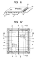
- Figs. 12 to 16 are a plan view, cross-sectional views, an equivalent circuit diagram and a perspective view of a pixel in a fifth example useful for understanding the present invention.
- Fig. 12 is a plan view of a pixel in a radiation detecting apparatus of the fifth example useful for understanding the present invention, illustrating a pixel, constituted of two switching elements and a conversion element, in a matrix array.
- Fig. 13 is a cross-sectional view along a line 13-13 in Fig. 12
- Fig. 14 is a cross-sectional view along a line 14-14 in Fig. 12 .
- a conversion element 1 is constituted of an MIS photoelectric conversion element, and an organic insulation layer is employed as an interlayer insulation layer between the switching elements 2 and the photoelectric conversion element.
- the present example is however naturally applicable to a structure not utilizing the organic insulation layer as shown in Figs. 3 to 5 .
- Fig. 15 is an equivalent circuit diagram of the radiation detecting apparatus shown in Fig. 12 , including a matrix array of 3 rows by 5 columns of the pixels each having two switching elements and a conversion element, and, in a peripheral part, a signal processing circuit 51, a resetting circuit 63, first and second gate driver circuits 61, 62 and a common electrode driver circuit 53.
- Fig. 16 is a view showing a schematic structure of the radiation detecting apparatus of the present example, showing an example having two or more driver circuits and a signal processing circuit in the peripheral part and a phosphor, for converting the radiation into a light such as a visible light, on the panel.
- the conversion element 1 in the present example is also constituted of an MIS photoelectric conversion element for converting a light such as a visible light or an infrared light into an electrical signal, and a phosphor as a wavelength converting member for converting a radiation into a light, such as a visible light, that can be photoelectrically converted by the photoelectric conversion element, is disposed thereon.
- a first switching element 11 constituted of a first TFT is used for transferring an electrical signal, obtained by a photoelectric conversion from a light, such as a visible light, in the conversion element 1, while a second switching element 12 constituted of a second TFT is intended to apply a certain potential to the conversion element 1 after the signal transfer, thereby removing a charge remaining in the conversion element 1 after the signal transfer (such operation being hereinafter called a resetting).
- the first switching element 11 is constituted, as shown in Fig. 12 , of a first electrode 13 constituting a source electrode, a second electrode 14 constituting a drain electrode and a first gate electrode 15, among which the first electrode 13 is connected with the signal wiring 6 while the second electrode 14 is connected with the pixel electrode 9 of the conversion element 1.
- the second switching element 12 is constituted of a third electrode 16 constituting a source electrode, a fourth electrode 17 constituting a drain electrode and a second gate electrode 18, among which the third electrode 16 is connected with a reset wiring 19 while the fourth electrode 17 is connected with the pixel electrode 9 of the conversion element 1.
- the conversion element 1 is formed in an area under from the pixel electrode 9 of the conversion element 1 to the bias wiring 8, and is disposed above the first switching element 11 and the second switching element 12.
- the pixel electrode 9 of the conversion element 1 is connected, via a through hole 10, with the second electrode 14 of the first switching element 11 and with the fourth electrode 17 of the second switching element 12.
- the first gate driver circuit 61 applies a turn-on voltage for the first switching element 11 to the first gate electrode 15, thereby transferring information to the signal processing circuit 51 to form an image. Thereafter, a turn-off voltage for the first switching element 11 is applied to the first gate electrode 15, thereby terminating the transfer. Then the second gate driver circuit 62 applies a turn-on voltage for the second switching element 12 to the second gate electrode 18, and a reset potential for the conversion element 1 is applied from the reset wiring 19. After the lapse of a predetermined period, a turn-off voltage for the second switching element 12 is applied to the second gate electrode 18, thereby terminating the resetting.
- Such separate drivings of the first switching element 11 and the second switching element 12 enable a signal transfer and a resetting at a high speed, thereby improving an image reading speed of the radiation detecting apparatus.
- the conversion element 1 is disposed above the first switching element 11, the second switching element 12, the first gate wiring 20, the second gate wiring 21, the signal wiring 6 and the reset wiring 19, and the first gate wiring 20, the second gate wiring 21, the signal wiring 6 and the reset wiring 19 are so disposed as to pass through an area between the normal projection area of the pixel electrode 9 on the substrate and the lower electrode 9, in such a manner that both ends of each wiring, opposite to each other in a width direction, are present in such area. Therefore, even in case of an alignment error in the exposure apparatus employed in the manufacturing process, each intersecting area remains constant to stabilize the capacitances in various parts, thereby preventing image artifacts resulting from variations in the capacitances in various parts.
- a large aperture rate can be secured by disposing the conversion element above the switching elements and the wirings. Also by disposing the switching element in the area between the normal projection area of the pixel electrode 9 on the substrate and the pixel electrode 9 as in the first example, the overlapping area between the pixel electrode 9 of the conversion element 1 and the electrode of the TFT 2 remains constant, thereby stabilizing the capacitance.
- all the wirings are so disposed as to pass through the area between the normal projection area of the pixel electrode 9 on the substrate and the pixel electrode 9, but it is also possible to dispose the signal wiring 6 only, or the first gate wiring 20 only, so as to pass through the area between the normal projection area of the pixel electrode 9 on the substrate and the pixel electrode 9. Also either one of the wirings (first gate wiring 20 and signal wiring 6) of the first switching element 11 and the wirings (second gate wiring 21 and reset wiring 19) of the second switching element 12 may be so disposed as to pass through the area between the normal projection area of the pixel electrode 9 on the substrate and the pixel electrode 9.
- a part of the wirings (first gate wiring 20 and signal wiring 6) of the first switching element 11 and a part of the wirings (second gate wiring 21 and reset wiring 19) of the second switching element 12 may be so disposed as to pass through the area between the normal projection area of the pixel electrode 9 on the substrate and the pixel electrode 9.
- Fig. 13 is a cross-sectional view along a line 13-13 in Fig. 12
- Fig. 14 which is a cross-sectional view along a line 14-14 in Fig. 12 .
- the first switching element 11 includes a first electrode layer 31 constituting the gate electrode and the gate wiring, a first insulation layer 32 constituting a gate insulation film, a first semiconductor layer 33, a first impurity-doped semiconductor layer 34 constituting an ohmic contact layer, and a second electrode layer 35 constituting a source electrode, a drain electrode and a signal wiring.
- the conversion element 1 is an MIS photoelectric converting element including a third electrode layer 37 (corresponding to the pixel electrode 9 in Fig. 12 ), a third insulation layer 38, a second semiconductor layer 39, a second impurity-doped semiconductor layer 40 functioning as an ohmic contact layer or a blocking layer, and a fifth electrode layer 42 (constituting an upper electrode), and is capable of a photoelectric conversion on a light such as a visible light.
- a fifth electrode layer 42 constituted of a transparent material such as ITO is disposed on the second impurity-doped semiconductor layer 40, but, in the case that the second impurity-doped semiconductor layer 40 has a low resistance, it may also serve as the electrode layer and the fifth electrode layer 42 may be dispensed with.
- a fourth electrode layer 41 is a bias wiring for a voltage application to the fifth electrode layer 42, and is connected to a common electrode driver circuit 53 provided outside the substrate.
- the fourth electrode layer 41 is covered by the fifth electrode layer 42, but it is also possible to dispose the fifth electrode layer 42 under the fourth electrode layer 41.
- the third electrode layer 37 is connected to one of the electrodes (drain electrode) formed by the second electrode layer 35 constituting the switching element 2, via a through hole formed in the second insulation layer 36. By turning on the switching element, a charge corresponding to the carriers generated in the second semiconductor layer 39 can be transferred to an external signal processing circuit (signal processing circuit 51 shown in Fig. 15 ).
- the third electrode layer 37 (pixel electrode of the conversion element 1) is so disposed as to cover the second electrode layer 35 constituting the signal wiring 6 and the reset wiring 19, and the first electrode layer 31 constituting the first gate wiring 20 and the second gate wiring 21.
- Such arrangement provides a structure that, in the area between the normal projection area of the pixel electrode 9 on the substrate and the pixel electrode 9, the signal wiring 6, the reset wiring 19, the first gate wiring 20 and the second gate wiring 21 are so disposed as to pass through such area in such a manner that both ends of each wiring opposite to each other in a width direction are present in such area.
- the overlapping area remains constant to suppress a capacitance variation in the pixel electrode 9.
- an organic insulation layer functioning as a planarization layer is employed as the second insulation layer 36 to be formed as the interlayer insulation layer between the switching element and the conversion element, thereby decreasing the capacity generated between the switching element and the conversion element.
- the fifth electrode layer 42 (upper electrode of the conversion element 1) is preferably so disposed as to cover the second electrode layer 35, constituting the signal wiring 6 and the reset wiring 19, and the first electrode layer 31, constituting the first gate wiring 20 and the second gate wiring 21.
- both the third electrode layer 37 (pixel electrode of the conversion element 1) and the fifth electrode layer 42 (upper electrode of the conversion element 1) are so disposed as to cover the second electrode layer 35, constituting the signal wiring 6 and the reset wiring 19, and the first electrode layer 31, constituting the first gate wiring 20 and the second gate wiring 21.
- An increase in a total capacity of the signal wiring 6, the first gate wiring and the second gate wiring leads to an increased noise in the image captured by the radiation detecting apparatus, or requires a larger time constant in a transfer operation of the TFT, whereby the image cannot be read at a high speed. It is therefore desirable to dispose, between the switching element 2 and the conversion element 1, an organic insulation layer that has a low dielectric constant and that can be formed in a thick film.
- the organic insulation layer is preferably formed with a material having a high heat resistance and a low dielectric constant, such as an acrylic resin or a polyimide, and is preferably formed with a thickness of 1 ⁇ m or larger in a thinnest part.
- the interlayer insulation layer need not be constituted of an organic insulation layer but may have a multi-layered structure constituted of an organic insulation layer and an inorganic insulation layer employed in Fig. 4 .
- a circuit including plural switching elements and a gate wiring within a pixel involves a complex arrangement of the wirings and the electrodes.
- a wiring is disposed between the conversion elements or the conversion element is disposed so as to involve an overlapping in a part of the wirings, the capacitances in various parts are not stabilized by an alignment error in the exposure apparatus employed in the manufacturing process, thus resulting in artifacts in the image.
- a stable manufacture is difficult because of the instability in the processed shapes.
- the characteristics and the manufacture can be stabilized by such a structure that the wirings are disposed, in an area below the pixel electrode, without protruding out from under the conversion element 1.
- the first gate driver circuit 61, the second gate driver circuit 62, the signal processing circuit 51 and the resetting circuit 63 are disposed in a peripheral portion of a panel, and a phosphor is disposed thereon, for converting a radiation into a light such as a visible light.
- the common electrode driver circuit 53 shown in Fig. 15 is incorporated in the signal processing circuit 51.
- Figs. 12 to 16 show a system of employing, as the conversion element 1, a photoelectric conversion element for converting a light such as a visible light into an electrical signal and depositing a phosphor directly thereon. But it is also possible to form a phosphor on a substrate of a radiation-transmitting material such as carbon and to adhere the surface of such phosphor with an adhesive material to a substrate bearing photoelectric conversion elements. It is also possible to utilize, as the conversion element 1, a semiconductor element for converting a radiation such as an X-ray, an ⁇ -ray a ⁇ -ray or a ⁇ -ray directly into an electrical signal, thereby dispensing with the phosphor.
- the semiconductor element capable of direct conversion of X-ray may include a semiconductor material such as amorphous selenium (a-Se).
- the pixel electrode of the conversion element is formed in a rectangular shape, and the signal wiring, the reset wiring and/or the gate wiring (or first and second gate wirings) is so disposed as to cross two parallel sides, opposed to each other, of the pixel electrode.
- the shape of the pixel electrode of the conversion element includes shapes considered to be substantially rectangular.
- a pixel electrode of a shape partly removed is also included.
- the two sides, opposed to each other, of the pixel electrode include a state close to parallel within an extent capable of covering the fluctuation in the capacitance.
- the present embodiment shows a constitution, in the pixel including two switching elements and a conversion element explained in the fifth example, of further reducing the fluctuation in the capacitance.
- a structure shown in Fig. 17 is different from that shown in Fig. 12 , in that the first switching element 11 for transfer and the second switching element 12 for resetting are disposed in positions of parallel displacement with respect to each other.
- first switching element 11 and the second switching element 12 have a same direction from an electrode, connected to the pixel electrode 9, to the other electrode, connected to the signal wiring 6 or the reset wiring 19.
- a direction from the first gate wiring 20 to an end of the first gate electrode is same as a direction from the second gate wiring 21 to an end of the second gate electrode.
- first switching element 11 and the second switching element 12 have an approximately same shape.
- Vth threshold voltage
- a voltage application higher than Vth turns on the TFT, thereby passing a current, and a voltage application lower than Vth turns off the TFT, thereby interrupting the current. This property is an important factor in a TFT matrix panel utilizing TFTs as the switching elements.
- Vth is shifted to a higher voltage. Therefore the TFT cannot be turned on unless a higher voltage is applied to the gate electrode, thereby resulting in a failure in the charge transfer.
- a turn-off voltage for TFT is applied.
- a turn-on voltage for the second switching element 12 is applied to apply the resetting potential to the pixel electrode 9 of the conversion element 1, a turn-off voltage is applied.
- the first switching element 11 and the second switching element 12 have different capacitances. Also after the first switching element 11 or the second switching element 12 is turned on, the charge is distributed among the capacitances (charge sharing), but the potential of the pixel electrode 9 after the transfer is different from the potential of the pixel electrode 9 after the resetting. Such difference between the potential of the pixel electrode 9 after the transfer and the potential after the resetting results in, for example, in a radiation detecting apparatus, a misdetection of a charge corresponding to such potential difference. Therefore, a mask alignment error in the formation of the switching element results in a potential fluctuation in the pixel electrode 9 within the pixel, and further results in a fluctuation in the pixel electrodes 9 within the TFT matrix panel.
- the constitution of the present embodiment is effective for reducing the artifacts resulting from a mask alignment error at the preparation of the switching element.
- the pixel electrode of the conversion element has a rectangular shape, but the shape and the layout of the pixel electrode is not limited to such rectangular shape but may be selected arbitrarily.
- the pixel electrodes 9 have a honeycomb structure, but the gate wiring 7 and the signal wiring 8 have a layout similar to that in the first and second examples.
- the pixel electrode of the conversion element has a rectangular shape, and the signal wiring 6 and/or the gate wiring 7 is so disposed as to cross parallel two sides, opposite to each other, of the pixel electrode.
- the gate wiring 7 passes two non-parallel sides, namely the obliquely patterned two sides of the pixel electrode 9, so as to pass through the area between the normal projection area of the pixel electrode 9 on the substrate and the pixel electrode 9.
- An alignment error between the gate wiring 7 and the pixel electrode 9 causes a certain change in the capacitance between the gate wiring and the pixel electrode in each pixel, and, in the prior structure, such capacitance change is large because the overlapping area is changed by a displacement of the gate wiring or the signal wiring in a width direction thereof.
- the overlapping area is changed by a displacement approximately in the longitudinal direction, so that the capacitance change is limited, whereby, in comparison with the prior structure, the capacitance can be stabilized with limited fluctuation to provide a captured image or a displayed image with suppressed artifacts.
- the process can be executed without the influence of the step difference whereby the conversion element can be formed in stable manner.
- the signal wiring 6 crosses two sides perpendicular to the signal wiring in the hexagonal pixel electrode 9, and is so disposed as to pass through an area between the normal projection area of the pixel electrode 9 on the substrate and the pixel electrode 9, in such a manner that both ends of the signal wiring 6, opposite to each other in a width direction, are present in such area.
- both wirings may be respectively so disposed as to cross the obliquely patterned two sides.
- such wiring is preferably positioned inside, by 1 to 3 ⁇ m or more, from the end of the pixel electrode.
- the alignment error between the layers in the process of forming conversion element may reach such area, as the specifications of an ordinary exposure apparatus involve an alignment error of about 1 ⁇ m in a use under a highly precise strict control or about 3 ⁇ m under an ordinary control.
- an error of about 1.5 times of the above-mentioned value depending on the structure of an alignment tree it is preferable, if possible, an inside positioning of about 10 ⁇ m.
- plural wirings are provided in the row direction or in the column direction with a pixel, it is more preferable that the wirings have an approximately same distance.
- an X-ray 6060 generated by an X-ray tube 6050 passes through a chest 6062 of an inspected person 6061 and enters a radiation detecting apparatus 6040.
- the incident X-ray contains information on the interior of body of the inspected person 6061.
- the phosphor of the radiation detecting apparatus 6040 emits a light, which is subjected to a photoelectric conversion to obtain electrical information.
- the information is converted into a digital signal which is subjected to an image processing by an image processor 6070 constituting signal processing means, and can be observed on a display 6080 constituting display means in a control room.
- this information can be transferred, by transmission means such as a telephone channel 6090, to a remote location and displayed on a display 6081 in a doctor room or recorded in a recording medium such as an optical disk by recording means such as an optical disk apparatus, for diagnosis by a doctor in a remote location.
- the information may also be recorded on a film 6110 by a laser printer 6101 of a film processor 6100.
- the present invention is applicable to a radiation detecting apparatus, utilizing a switching element and a conversion element, for medical purpose and for nondestructive inspection. It is also applicable to a detecting apparatus for converting a light such as a visible light into an electrical signal, particularly to a detecting apparatus having a large-area photoelectric conversion area.
Description
- The present invention relates to a radiation detecting apparatus for converting a radiation into an electrical signal, and to a radiation detecting system utilizing such radiation detecting apparatus.
- Recently, a radiation detecting apparatus, which incorporates, on an insulating substrate, pixels each formed by a TFT (thin film transistor) as a switching element and a conversion element for converting a radiation such as an X-ray into an electrical signal, is being commercially utilized. The conversion element includes, for example, following two types. One is an indirect type conversion element constituted of a photoelectric conversion element and a wavelength conversion member (such as a phosphor) for converting a radiation such as an X-ray into a light of a wavelength region detectable by the photoelectric conversion element. Such indirect type conversion element executes a wavelength conversion of the radiation such as X-ray into a light, by means of a wavelength conversion member such as a phosphor, disposed on a photoelectric conversion element, and executes a photoelectric conversion on the light from the wavelength conversion member by the photoelectric conversion element. The other is a direct type conversion element which directly converts the radiation such as an X-ray into an electrical signal, by means of a direct conversion semiconductor element including a semiconductor conversion material, capable of converting the radiation such as an X-ray into the electrical signal, such as amorphous selenium (a-Se).
- In such radiation detecting apparatus, a higher speed and a higher sensitivity are being required. For this purpose, it is required, while increasing the size of the switching element or providing plural switching elements for increasing the driving speed, to secure a large area of the conversion element thereby detecting a larger amount of the radiation entering from above or of the light converted from the radiation. The conversion element includes at least an upper electrode, a lower electrode and a semiconductor layer for converting the radiation into the electrical signal or a semiconductor layer for converting the light into the electrical signal, disposed between the upper and lower electrodes, and either one of the electrodes is two-dimensionally divided for pixel isolation, thereby realizing a two-dimensional array of pixels.
- In the prior radiation detecting apparatus,
U.S. Patent No. 6,020,590 describes disposing a conversion element part, including a direct conversion semiconductor element, on a switching element part containing the switching element such as TFT. As another example, in a radiation detecting apparatus disclosed in Japanese Patent Application Laid-open No.2004-015002 Fig. 20 ). The pixel electrode of the conversion element part is divided on the signal wiring, connected to the source electrode or the drain electrode of the TFT constituting the switching element part, and on the gate wiring. - Further, the document
JP 2004 265935 A - The document
WO 2004 73068 - An object of the present invention is to provide a radiation detecting apparatus and a radiation detecting system utilizing such radiation detecting apparatus, capable of realizing a higher definition in a captured image, and having a more easily manufacturable structure.
- According to an aspect of the present invention, there is provided a radiation detecting apparatus as defined in claim1
- According to another aspect of the present invention, there is provided a radiation detecting system as defined in
claim 12. - In the present specification, "arranged in one direction" or "arranged in a direction different from the aforementioned one direction" means not only an arrangement in a linear array but also includes a case where a switching element is disposed on both sides on a wiring, as in a case of gate wiring shown in
Fig. 18 . - In the present invention, the conversion element for converting a radiation into an electrical signal means an element capable of receiving a radiation such as a visible light, an infrared light, an X-ray, an α-ray, a β-ray or a γ-ray and converting it into an electrical signal, and includes a photoelectric conversion element for converting a light such as a visible light or an infrared light into an electrical signal, and an element including for example amorphous selenium as a semiconductor layer and capable of converting a radiation such as an X-ray into an electrical signal.
- In a radiation detecting apparatus including a plurality of pixels each having a conversion element for converting a radiation into an electrical signal and a switching element, the present invention allows to reduce and stabilize a variation in a capacity between a wiring connected with the switching element and an electrode of the conversion element, thereby providing a radiation detecting apparatus of stabilized characteristics. And capable of providing a captured image or a displayed image for example with suppressed artifacts.
- Also the present invention allows to dispense with a strict alignment between a wiring connected with the switching element and an electrode of the conversion element and also allows a manufacture with a reduced influence of a step difference caused by wirings, thereby facilitating the manufacturing process.
- Other features and advantages of the present invention will be apparent from the following description taken in conjunction with the accompanying drawings, in which like reference characters designate the same or similar parts throughout the figures thereof.
- The accompanying drawings, which are incorporated in and constitute a part of the specification, illustrate embodiments of the invention and, together with the description, serve to explain the principles of the invention.
-
Fig. 1 is a plan view showing a structure of a pixel in a first example which is useful for understanding the present invention. -
Fig. 2 is a cross-sectional view along a line 2-2 inFig. 1 . -
Fig. 3 is a plan view showing a structure of a pixel in a second example which is useful for understanding the present invention. -
Fig. 4 is a cross-sectional view along a line 4-4 inFig. 3 . -
Fig. 5 is a cross-sectional view along a line 5-5 inFig. 3 . -
Fig. 6 is a cross-sectional view showing a structure of a pixel in a third example which is useful for understanding the present invention, corresponding to a cross section along a line 4-4 inFig. 3 . -
Fig. 7 is a cross-sectional view showing a structure of a pixel in a third example which is useful for understanding the present invention, corresponding to a cross section along a line 5-5 inFig. 3 . -
Fig. 8 is a cross-sectional view showing a structure of a pixel in a fourth example which is useful for understanding the present invention, corresponding to a cross section along a line 4-4 inFig. 3 . -
Fig. 9 is a cross-sectional view showing a structure of a pixel in a third example which is useful for understanding the present invention, corresponding to a cross section along a line 5-5 inFig. 3 . -
Fig. 10 is an equivalent circuit diagram showing a radiation detecting apparatus in which a pixel of the examples shown inFigs. 1 to 9 is arranged in a matrix pattern. -
Fig. 11 is a perspective view showing a radiation detecting apparatus in which a pixel of the examples shown inFigs. 1 to 9 is arranged in a matrix pattern. -
Fig. 12 is a plan view showing a structure of a pixel in a fifth example which is useful for understanding the present invention. -
Fig. 13 is a cross-sectional view along a line 13-13 inFig. 12 . -
Fig. 14 is a cross-sectional view along a line 14-14 inFig. 12 . -
Fig. 15 is an equivalent circuit diagram of the pixel shown inFig. 12 . -
Fig. 16 is a view showing a schematic structure of a radiation detecting apparatus in the fifth example which is useful for understanding the present invention. -
Fig. 17 is a plan view of a pixel in a first embodiment of the present invention. -
Fig. 18 is a plan view of a pixel in a sixth example which is useful for understanding the present invention. -
Fig. 19 is a view showing a radiation detecting system employing a radiation detecting apparatus of a second embodiment of the present invention. -
Fig. 20 is a plan view showing an example of a pixel in a prior radiation detecting apparatus. -
Fig. 21 is a schematic view showing a state in which a signal wiring or a gate wiring passes through a area between a normal projection area of thelower electrode 9 onto a substrate and thelower electrode 9. - In the following, examples which are useful for understanding the present invention and embodiments of the present invention will be explained in detail with reference to the accompanying drawings.
- The radiation detecting apparatus of the present invention will be explained in detail by an example of a radiation detecting apparatus for converting a radiation such as an X-ray into an electrical signal. But it is not limited to such radiation detecting apparatus but is applicable also to a detecting apparatus which converts a light, such as a visible light or an infrared light, into an electrical signal.
- In the following, a radiation detecting apparatus, constituting a first example useful for understanding the present invention, will be explained. The present example has a structure in which a signal wiring or a gate wiring, constituting a control wiring, passes under a pixel electrode, isolated for each pixel, of a conversion element constituted of a photoelectric conversion element.
Figs. 1 and 2 illustrate a case in which the signal wiring is disposed under the pixel electrode. -
Fig. 1 is a plan view showing a structure of a pixel in the radiation detecting apparatus of the first example, illustrating a pixel including a switching element formed by a TFT and a conversion element and to be disposed in a two-dimensional matrix array.Fig. 2 is a cross-sectional view along a line 2-2 inFig. 1 . -
Figs. 10 and11 are respectively an equivalent circuit diagram and a perspective view of a radiation detecting apparatus, in which the pixel shown inFigs. 1 and 2 is arranged in a matrix array. - Referring to
Fig. 1 , aconversion element 1 is constituted of an MIS photoelectric conversion element of a metal-insulator-semiconductor structure for converting a light, such as a visible light or an infrared light, into an electrical signal. And a phosphor (not shown inFig. 1 ) is disposed thereon as a wavelength converting member for converting a radiation such as an X-ray, an α-ray a β-ray or a γ-ray into a light, such as a visible light, that can be photoelectrically converted in the MIS photoelectric conversion element. The phosphor may be constituted, for example, of CsI which converts an X-ray into a light. - A switching
element 2, constituted of a TFT (thin film transistor) and functioning as a switching element, has three electrodes, including asource electrode 3 and adrain electrode 4 as two terminals, and agate electrode 5 serving as a control terminal. A channel of theswitching element 2 exists between thesource electrode 3 and thedrain electrode 4, and a charge flow in the channel can be controlled by a voltage control on thegate electrode 5. - The
conversion element 1 has a layered structure from apixel electrode 9 isolated for each pixel to a region under thebias wiring 8, and is disposed on theswitching element 2. Thepixel electrode 9 of theconversion element 1 is connected, via a throughhole 10, to thedrain electrode 4 of theswitching element 2. - Now reference is made to
Fig. 2 , showing a cross-sectional view along a line 2-2 inFig. 1 , for explaining the layered structure of a pixel in the first example. The switchingelement 2 is disposed on a substrate, then theconversion element 1 is disposed thereon, and aphosphor layer 44 is disposed further thereon. - The switching
element 2 includes afirst electrode layer 31 constituting a gate electrode (corresponding to thegate electrode 5 inFig. 1 ) and a gate wiring (corresponding to thegate wiring 7 inFig. 1 ), afirst insulation layer 32 constituting a gate insulation film, afirst semiconductor layer 33, a first impurity-dopedsemiconductor layer 34 constituting an ohmic contact layer, and asecond electrode layer 35 constituting source and drain electrodes (corresponding to thesource electrode 3 and thedrain electrode 4 inFig. 1 ) and a signal wiring (corresponding thesignal wiring 6 inFig. 1 ). - The
conversion element 1 is an MIS photoelectric converting element including athird electrode layer 37 isolated for each pixel (corresponding to thepixel electrode 9 inFig. 1 ), athird insulation layer 38, asecond semiconductor layer 39, a second impurity-dopedsemiconductor layer 40 functioning as an ohmic contact layer or a blocking layer, and a fifth electrode layer 42 (constituting an upper electrode), and is capable of a photoelectric conversion on a light such as a visible light. Afifth electrode layer 42 constituted of a transparent material such as ITO is disposed on the second impurity-dopedsemiconductor layer 40, but, in the case that the second impurity-dopedsemiconductor layer 40 has a low resistance, it may also serve as the electrode layer and thefifth electrode layer 42 may be dispensed with. In such case, the second impurity-dopedsemiconductor layer 40 serves as an upper electrode of theconversion element 1. - A
fourth electrode layer 41 is a bias wiring (corresponding to abias wiring 8 inFig. 1 ) for a voltage application to thefifth electrode layer 42, and is connected to a common electrode driver circuit (commonelectrode driver circuit 53 inFig. 10 ). Thefourth electrode layer 41 is covered by thefifth electrode layer 42, but it is also possible to dispose thefifth electrode layer 42 under thefourth electrode layer 41. The third electrode layer 37 (corresponding to thepixel electrode 9 inFig. 1 ) of theconversion element 1 is connected to one of the electrodes (drain electrode) formed by thesecond electrode layer 35 constituting the switchingelement 2, via a through hole (corresponding to the throughhole 10 inFig. 1 ) formed in thesecond insulation layer 36 constituting the interlayer insulation layer. By turning on theswitching element 2, a charge corresponding to the carriers generated in thesecond semiconductor layer 39 of theconversion element 1 can be transferred to an external signal processing circuit (signal processing circuit 51 shown inFig. 10 ). - In the present example, as will be understood from the structures shown in
Figs. 1 and 2 , in an area between a normal projection area of thepixel electrode 9 on the substrate and thepixel electrode 9, thesignal wiring 6 is so disposed as to pass through such area in such a manner that both ends thereof opposite to each other in a width direction are present in such area (passing through under thepixel electrode 9 of theconversion element 1 without jetting out). In such structure, even in the case that the positional relationship of thesignal wiring 6 and thepixel electrode 9 of theconversion element 1 is displaced by an alignment error in the exposure apparatus employed in the manufacturing process, the overlapping area of thesignal wiring 6 and thepixel electrode 9 of theconversion element 1 remains same to maintain a constant capacitance between thesignal wiring 6 and thepixel electrode 9 of theconversion element 1. Whereby image artifacts, resulting from a fluctuation in the capacitance in the pixel, can be suppressed in the image obtained by the radiation detecting apparatus. - A similar effect can be obtained by disposing the
gate wiring 7, in an area between a normal projection area of thepixel electrode 9 on the substrate and thepixel electrode 9, so as to pass through such area in such a manner that both ends opposite to each other in a width direction are present in such area (so as to be inside the electrode area when seen from above the conversion element, or so as that thegate electrode 7 passes through under thepixel electrode 9 of theconversion element 1 without jetting out). It is therefore also possible to dispose thegate wiring 7 alone so as to pass through inside such area. However it is considered more important to dispose thesignal wiring 6 so as to pass through under thepixel electrode 9 without jetting out, since thesignal wiring 6 handles a small charge converted in each pixel and a variation in the capacitance of the signal wiring is directly reflected as an image artifact. - Also a similar effect can be obtained by disposing the
switching element 2 within an area between a normal projection area of thepixel electrode 9 on the substrate and thepixel electrode 9. In the case that a part of thesource electrode 3 or thedrain electrode 4 of theswitching element 2 protrudes out from under thepixel electrode 9 and is disposed in an adjacent pixel area, a variation of the capacitance among the pixels is caused by a displaced positional relationship, induced by an alignment error in the exposure apparatus employed in the manufacturing process. The above-described constitution provides similar effects in all the examples and embodiments of the radiation detecting apparatus of the present specification. -
Fig. 21 schematically shows a state in which asignal wiring 6 or agate wiring 7 passes through anarea 101 between anormal projection area 102 of thepixel electrode 9 onto thesubstrate 100 and thepixel electrode 9. - As will be seen from the layered structure shown in
Fig. 2 , the third electrode layer 37 (pixel electrode of the conversion element 1) is so disposed as to cover thesecond electrode layer 35 constituting thesignal wiring 6. Such arrangement provides a structure that, in the area between the normal projection area of thepixel electrode 9 on the substrate and thepixel electrode 9, thesignal wiring 6 is so disposed as to pass through such area in such a manner that both ends thereof opposite to each other in a width direction are present in such area. Therefore, even in case of an alignment error in the exposure apparatus employed in the manufacturing process, the overlapping area remains constant to suppress a capacitance variation in thepixel electrode 9. Also the fifth electrode layer 42 (upper electrode of the conversion element 1) is preferably so disposed as to cover thesecond electrode layer 35, constituting thesignal wiring 6. And in the present example, both the third electrode layer 37 (pixel electrode of the conversion element 1) and the fifth electrode layer 42 (upper electrode of the conversion element 1) are so disposed as to cover thesecond electrode layer 35 constituting thesignal wiring 6. In the case that the third electrode layer 37 (pixel electrode of the conversion element 1) is so constructed as to cover thegate wiring 7, it is naturally preferable that the fifth electrode layer 42 (upper electrode of the conversion element 1) is also so disposed as to cover thegate wiring 7. Also in the case that the third electrode layer 37 (pixel electrode of the conversion element 1) is so constructed as to cover theswitching element 2, it is naturally preferable that the fifth electrode layer 42 (upper electrode of the conversion element 1) is also so disposed as to cover theswitching element 2. - Now reference is made to
Figs. 10 and11 , for explaining a constitution of a radiation detecting apparatus, formed by disposing the pixels, explained inFigs. 1 and 2 , in a matrix array. - As shown in
Fig. 10 , pixels each having aconversion element 1 and aswitching element 2 are arrayed in a two-dimensional matrix on a substrate. Andgate wirings 7 connected to thegate electrodes 5 of theswitching elements 2 andsignal wirings 6 connected to thesource electrodes 3 of theswitching elements 2 are provided respectively by a number corresponding a number of rows of the pixels and by a number corresponding to a number of columns of the pixels. In a peripheral portion of the substrate, asignal processing circuit 51, a commonelectrode driver circuit 52 and agate driver circuit 52 are disposed. Agate wiring 7, connected with thegate electrode 5 of theswitching element 2, is connected with thegate driver circuit 52 for on/off controlling theswitching element 2, and asignal wiring 6, connected with thesource electrode 3 of theswitching element 2, is connected with thesignal processing circuit 41 for reading and processing an accumulated charge. Also abias wiring 8, connected with an electrode (upper electrode) of theconversion element 1, is connected with the commonelectrode driver circuit 53. - As shown in
Fig. 11 , thegate driver circuit 52 and thesignal processing circuit 51 are disposed in a peripheral portion of a panel, and a phosphor is disposed thereon, for converting a radiation into a light such as a visible light.Fig. 10 shows thesignal processing circuit 51 and the commonelectrode driver circuit 53 separately, but in fact the commonelectrode driver circuit 53 is incorporated in thesignal processing circuit 51 as shown inFig. 11 . Thegate driver circuit 52 and thesignal processing circuit 51 are connected to thesubstrate 50 through a TCP (tape carrier package: a film carrying an IC) carrying an IC.Fig. 11 shows a system of converting a radiation by the phosphor into a light such as a visible light and then executing a photoelectric conversion by the photoelectric conversion element, but it is also possible to utilize a semiconductor element for converting a radiation such as an X-ray, an α-ray a β-ray or a γ-ray directly into an electrical signal as theconversion element 1, thereby dispensing with the phosphor. The semiconductor element capable of direct conversion of X-ray may include a semiconductor material such as amorphous selenium (a-Se). Also there has been explained a structure employing a photoelectric conversion element for converting a light such as a visible light into an electrical signal and depositing a phosphor such as CsI directly thereon. But it is also possible to form a phosphor on a substrate of a radiation-transmitting material such as carbon and to adhere the surface of such phosphor with an adhesive material to a substrate bearing pixels each having theconversion element 1 and theswitching element 2. - The present example shows a case in which a signal wiring and a gate wiring pass through under a pixel electrode.
-
Fig. 3 is a plan view showing a structure of a pixel in the second example useful for understanding the present invention,Fig. 4 is a cross-sectional view along a line 4-4 inFig. 3 , andFig. 5 is a cross-sectional view along a line 5-5 inFig. 3 . InFigs. 4 and5 , components same as or equivalent to those inFig. 2 are represented by like characters and not explained further. Also the constitution of the radiation detecting apparatus formed by a two-dimensional matrix array of pixels is same as that inFigs. 10 and11 . - A
conversion element 1 is constituted, as in the example 1, of an MIS photoelectric conversion element. On the MIS photoelectric conversion element, a phosphor such as CsI is disposed as a wavelength converting member for converting a radiation such as an X-ray, an α-ray a β-ray or a γ-ray into a light, such as a visible light, that can be photoelectrically converted in the MIS photoelectric conversion element. - In the structure of the example 1 shown in
Fig. 1 , thesignal wiring 6 is so disposed, in the area between the normal projection area of thepixel electrode 9 on the substrate and thepixel electrode 9, as to pass through such area in such a manner that both ends opposite to each other in a width direction are present in such area (so as to be inside the electrode area without jetting out). In the present example shown inFig. 3 , not only thesignal wiring 6 but also thegate wiring 7 are so disposed as to pass through the aforementioned area in such a manner that both ends opposite to each other in a width direction are present in such area. - As will be seen from
Fig. 4 , the third electrode layer 37 (pixel electrode of the conversion element 1) is so disposed as to cover thesecond electrode layer 35 constituting thesignal wiring 6. Such arrangement provides a structure that, in the area between the normal projection area of thepixel electrode 9 on the substrate and thepixel electrode 9, thesignal wiring 6 is so disposed as to pass through such area in such a manner that both ends thereof opposite to each other in a width direction are present in such area. Therefore, even in case of an alignment error in the exposure apparatus employed in the manufacturing process, the overlapping area remains constant to suppress a capacitance variation in thepixel electrode 9. Also the fifth electrode layer 42 (upper electrode of the conversion element 1) is preferably so disposed as to cover thesecond electrode layer 35, constituting thesignal wiring 6. And in the present example, both the third electrode layer 37 (pixel electrode of the conversion element 1) and the fifth electrode layer 42 (upper electrode of the conversion element 1) are so disposed as to cover thesecond electrode layer 35 constituting thesignal wiring 6. - Also as will be seen from
Fig. 5 , the third electrode layer 37 (pixel electrode of the conversion element 1) is so disposed as to cover thefirst electrode layer 31 constituting thegate wiring 7. Such arrangement provides a structure that, in the area between the normal projection area of thepixel electrode 9 on the substrate and thepixel electrode 9, thegate wiring 7 is so disposed as to pass through such area in such a manner that both ends of thegate wiring 7 opposite to each other in a width direction are present in such area. Therefore, even in case of an alignment error in the exposure apparatus employed in the manufacturing process, the overlapping area remains constant to suppress a capacitance variation in thepixel electrode 9. Also the fifth electrode layer 42 (upper electrode of the conversion element 1) is preferably so disposed as to cover thefirst electrode layer 31, constituting thegate wiring 7. And in the present example, both the third electrode layer 37 (pixel electrode of the conversion element 1) and the fifth electrode layer 42 (upper electrode of the conversion element 1) are so disposed as to cover thefirst electrode layer 31 constituting thegate wiring 7. - In such structure, even in the case that the positional relationship of the
signal wiring 6 and thepixel electrode 9 of theconversion element 1 is displaced by an alignment error in the exposure apparatus employed in the manufacturing process, the overlapping area of thesignal wiring 6 and thepixel electrode 9 of theconversion element 1 remains same to maintain a constant capacitance between thesignal wiring 6 and thepixel electrode 9 of theconversion element 1, whereby image artifacts, resulting from a fluctuation in the capacitance in the pixel, can be suppressed in the image obtained by the radiation detecting apparatus. Also as regards thegate wiring 7, the overlapping area of thegate wiring 7 and thepixel electrode 9 of theconversion element 1 remains constant, even in case of a displacement in the positional relationship by an alignment error, thereby stabilizing the capacitance of thegate wiring 7. Therefore a transfer ability is stabilized among the pixels, and image artifacts, resulting from a fluctuation in the transfer ability among the pixels, can be suppressed. - Also as in the first example, by disposing the
switching element 2 in the area between the normal projection area of thepixel electrode 9 on the substrate and thepixel electrode 9, the overlapping area between thepixel electrode 9 of theconversion element 1 and theswitching element 2 remains constant thereby stabilizing the capacitance. -
Figs. 3 to 5 show a system of employing a photoelectric conversion element for converting a light such as a visible light into an electrical signal and depositing a phosphor directly thereon. But it is also possible to form a phosphor on a substrate of a radiation-transmitting material such as carbon and to adhere the surface of such phosphor with an adhesive material to a substrate bearing photoelectric conversion elements. It is also possible to utilize a semiconductor element for converting a radiation such as an X-ray, an α-ray a β-ray or a γ-ray directly into an electrical signal as theconversion element 1, thereby dispensing with the phosphor. The semiconductor element capable of direct conversion of X-ray may include a semiconductor material such as amorphous selenium (a-Se). - The present example shows a case in which an organic insulation layer is provided as a planarization film between the switching
element 2 and theconversion element 1. -
Figs. 6 and7 are cross-sectional views showing a structure of a pixel in a radiation detecting apparatus in the third example useful for understanding the present invention. The pixel in a plan view has a structure same as that shown inFig. 3 .Fig. 6 is a cross-sectional view along a line 4-4 inFig. 3 , andFig. 7 is a cross-sectional view along a line 5-5 inFig. 3 . The constitution of the radiation detecting apparatus formed by a two-dimensional matrix array of pixels is same as that inFigs. 10 and11 . As a conversion element, an MIS photoelectric conversion element including a structure of metal film-insulation layer-semiconductor layer is utilized as in the first and second examples. - In the following, the constitution will be explained with reference to the cross-sectional views shown in
Figs. 6 and7 . InFigs. 6 and7 , components same as or equivalent to those inFigs. 4 and5 are represented by like characters and not explained further. - The structure shown in
Figs. 6 and7 is different, from that shown inFigs. 4 and5 , in the use, as thesecond insulation layer 36 between the switchingelement 2 and theconversion element 1, of an organic interlayer insulation film, which has a function as a planarization layer. It is thus rendered possible to reduce a capacitance, formed between the switchingelement 2 and theconversion element 1. An increase in a total capacity of the signal wiring and the gate wiring leads to an increased noise in the image captured by the radiation detecting apparatus, or requires a larger time constant in a transfer operation of the TFT, whereby the image cannot be read at a high speed. It is therefore desirable to dispose, between the switchingelement 2 and theconversion element 1, an organic insulation layer that has a low dielectric constant and that can be formed in a thick film. - The organic insulation layer is preferably formed with a material having a high heat resistance and a low dielectric constant, such as an acrylic resin or a polyimide, and is preferably formed with a thickness of 1 µm or larger in a thinnest part. The organic insulation layer may be formed, for example by BCB (benzocyclobutene) produced by Dow Chemical Inc. The interlayer insulation layer need not be constituted of an organic insulation layer but may have a multi-layered structure constituted of an organic insulation layer and an inorganic insulation layer employed in
Fig. 4 . - As will be seen from
Fig. 6 , the third electrode layer 37 (pixel electrode of the conversion element 1) is so disposed as to cover thesecond electrode layer 35 constituting thesignal wiring 6. Such arrangement provides a structure that, in the area between the normal projection area of thepixel electrode 9 on the substrate and thepixel electrode 9, thesignal wiring 6 is so disposed as to pass through such area in such a manner that both ends thereof opposite to each other in a width direction are present in such area. Therefore, even in case of an alignment error in the exposure apparatus employed in the manufacturing process, the overlapping area remains constant to suppress a capacitance variation in thepixel electrode 9. Also the fifth electrode layer 42 (upper electrode of the conversion element 1) is preferably so disposed as to cover thesecond electrode layer 35, constituting thesignal wiring 6. And in the present example, both the third electrode layer 37 (pixel electrode of the conversion element 1) and the fifth electrode layer 42 (upper electrode of the conversion element 1) are so disposed as to cover thesecond electrode layer 35 constituting thesignal wiring 6. - Also as will be seen from
Fig. 7 , the third electrode layer 37 (pixel electrode of the conversion element 1) is so disposed as to cover thefirst electrode layer 31 constituting thegate wiring 7. Such arrangement provides a structure that, in the area between the normal projection area of thepixel electrode 9 on the substrate and thepixel electrode 9, thegate wiring 7 is so disposed as to pass through such area in such a manner that both ends of thegate wiring 7 opposite to each other in a width direction are present in such area. Therefore, even in case of an alignment error in the exposure apparatus employed in the manufacturing process, the overlapping area remains constant to suppress a capacitance variation in thepixel electrode 9. Also the fifth electrode layer 42 (upper electrode of the conversion element 1) is preferably so disposed as to cover thefirst electrode layer 31, constituting thegate wiring 7. And in the present example, both the third electrode layer 37 (pixel electrode of the conversion element 1) and the fifth electrode layer 42 (upper electrode of the conversion element 1) are so disposed as to cover thefirst electrode layer 31 constituting thegate wiring 7. - Also as in the first example, by disposing the
switching element 2 in the area between the normal projection area of thepixel electrode 9 on the substrate and thepixel electrode 9, the overlapping area between thepixel electrode 9 of theconversion element 1 and theswitching element 2 remains constant thereby stabilizing the capacitance. -
Figs. 6 and7 show a system of employing a photoelectric conversion element for converting a light such as a visible light into an electrical signal and depositing a phosphor directly thereon, but it is also possible to form a phosphor on a substrate of a radiation-transmitting material such as carbon and to adhere the surface of such phosphor with an adhesive material to a substrate bearing photoelectric conversion elements. It is also possible to utilize a semiconductor element for converting a radiation such as an X-ray, an α-ray a β-ray or a γ-ray directly into an electrical signal as theconversion element 1, thereby dispensing with the phosphor. The semiconductor element capable of direct conversion of X-ray may include a semiconductor material such as amorphous selenium (a-Se). - The structure of the present example is applicable, as in the first example, also to a case where the
signal wiring 6 alone is disposed so as to pass through the area between the normal projection area of thepixel electrode 9 on the substrate and thepixel electrode 9. And also to a case where thegate wiring 7 alone is disposed so as to pass through the area between the normal projection area of thepixel electrode 9 on the substrate and thepixel electrode 9. - The present example shows a structure of disposing a PIN photoelectric conversion element, constituted of an n-impurity-doped semiconductor layer, a semiconductor layer and a p-impurity-doped semiconductor layer as the
conversion element 1, on thesignal wiring 6 and theswitching element 2, and utilizing an organic insulation layer between the switchingelement 2 and theconversion element 1. -
Figs. 8 and9 are cross-sectional views showing a structure of a pixel in a radiation detecting apparatus in the fourth example useful for understanding the present invention. The pixel in a plan view has a structure same as that shown inFig. 3 .Fig. 8 is a cross-sectional view along a line 4-4 inFig. 3 , andFig. 9 is a cross-sectional view along a line 5-5 inFig. 3 . InFigs. 8 and9 , components same as or equivalent to those inFigs. 4 and5 are represented by like characters and not explained further. The constitution of the radiation detecting apparatus formed by a two-dimensional matrix array of pixels is same as that inFigs. 10 and11 . - In the following, the constitution will be explained with reference to the cross-sectional views shown in
Figs. 8 and9 . - The structure shown in
Figs. 8 and9 is different, from those shown inFigs. 4 to 7 , in using an organic insulation layer as thesecond insulation layer 36 to be formed as the interlayer insulation layer between the switchingelement 2 and theconversion element 1, and disposing, as theconversion element 1, a PIN photoelectric conversion element constituted of a second n-impurity-dopedsemiconductor layer 40, asecond semiconductor layer 39 and a third p-impurity-dopedsemiconductor layer 45. As will be seen fromFig. 8 , the third electrode layer 37 (pixel electrode of the conversion element 1) is so disposed as to cover thesecond electrode layer 35 constituting thesignal wiring 6. Such arrangement provides a structure that, in the area between the normal projection area of thepixel electrode 9 on the substrate and thepixel electrode 9, thesignal wiring 6 is so disposed as to pass through such area in such a manner that both ends thereof opposite to each other in a width direction are present in such area. Therefore, even in case of an alignment error in the exposure apparatus employed in the manufacturing process, the overlapping area remains constant to suppress a capacitance variation in thepixel electrode 9. Also the fifth electrode layer 42 (upper electrode of the conversion element 1) is preferably so disposed as to cover thesecond electrode layer 35, constituting thesignal wiring 6. And in the present example, both the third electrode layer 37 (pixel electrode of the conversion element 1) and the fifth electrode layer 42 (upper electrode of the conversion element 1) are so disposed as to cover thesecond electrode layer 35 constituting thesignal wiring 6. - Also as will be seen from
Fig. 9 , the third electrode layer 37 (pixel electrode of the conversion element 1) is so disposed as to cover thefirst electrode layer 31 constituting thegate wiring 7. Such arrangement provides a structure that, in the area between the normal projection area of thepixel electrode 9 on the substrate and thepixel electrode 9, thegate wiring 7 is so disposed as to pass through such area in such a manner that both ends of thegate wiring 7 opposite to each other in a width direction are present in such area. Therefore, even in case of an alignment error in the exposure apparatus employed in the manufacturing process, the overlapping area remains constant to suppress a capacitance variation in thepixel electrode 9. Also the fifth electrode layer 42 (upper electrode of the conversion element 1) is preferably so disposed as to cover thefirst electrode layer 31, constituting thegate wiring 7, and, in the present example, both the third electrode layer 37 (pixel electrode of the conversion element 1) and the fifth electrode layer 42 (upper electrode of the conversion element 1) are so disposed as to cover thefirst electrode layer 31 constituting thegate wiring 7. - Also as in the first example, by disposing the
switching element 2 in the area between the normal projection area of thepixel electrode 9 on the substrate and thepixel electrode 9, the overlapping area between thepixel electrode 9 of theconversion element 1 and theswitching element 2 remains constant thereby stabilizing the capacitance. -
Figs. 8 and9 show a system of employing a photoelectric conversion element for converting a light such as a visible light into an electrical signal and depositing a phosphor directly thereon. But it is also possible to form a phosphor on a substrate of a radiation-transmitting material such as carbon and to adhere the surface of such phosphor with an adhesive material to a substrate bearing photoelectric conversion elements. It is also possible to utilize a semiconductor element for converting a radiation such as an X-ray, an α-ray a β-ray or a γ-ray directly into an electrical signal as theconversion element 1, thereby dispensing with the phosphor. The semiconductor element capable of direct conversion of X-ray may include a semiconductor material such as amorphous selenium (a-Se). - The structure of the present example is applicable, as in the first example, also to a case where the
signal wiring 6 alone is so disposed to pass through under thepixel electrode 9 of the conversion element without protruding therefrom. And also to a case where thegate wiring 7 alone is so disposed to pass through under thepixel electrode 9 of the conversion element without protruding therefrom. - The foregoing examples have shown structures where both the
pixel electrode 9 of theconversion element 1 and the fifth electrode layer 42 (upper electrode) are so disposed as to cover theswitching element 2 and thesignal wiring 6 or thegate wiring 7. But there may be adopted a structure in which thepixel electrode 9 of theconversion element 1 covers the switchingelement 2 and thesignal wiring 6 or thegate wiring 7. Thesecond semiconductor layer 39 or thefifth electrode layer 42, disposed on the pixel electrode need not be isolated in each pixel but may be mutually connected among the pixels. -
Figs. 12 to 16 are a plan view, cross-sectional views, an equivalent circuit diagram and a perspective view of a pixel in a fifth example useful for understanding the present invention. -
Fig. 12 is a plan view of a pixel in a radiation detecting apparatus of the fifth example useful for understanding the present invention, illustrating a pixel, constituted of two switching elements and a conversion element, in a matrix array.Fig. 13 is a cross-sectional view along a line 13-13 inFig. 12 , andFig. 14 is a cross-sectional view along a line 14-14 inFig. 12 . Aconversion element 1 is constituted of an MIS photoelectric conversion element, and an organic insulation layer is employed as an interlayer insulation layer between the switchingelements 2 and the photoelectric conversion element. The present example is however naturally applicable to a structure not utilizing the organic insulation layer as shown inFigs. 3 to 5 . -
Fig. 15 is an equivalent circuit diagram of the radiation detecting apparatus shown inFig. 12 , including a matrix array of 3 rows by 5 columns of the pixels each having two switching elements and a conversion element, and, in a peripheral part, asignal processing circuit 51, a resettingcircuit 63, first and secondgate driver circuits electrode driver circuit 53. -
Fig. 16 is a view showing a schematic structure of the radiation detecting apparatus of the present example, showing an example having two or more driver circuits and a signal processing circuit in the peripheral part and a phosphor, for converting the radiation into a light such as a visible light, on the panel. - The
conversion element 1 in the present example is also constituted of an MIS photoelectric conversion element for converting a light such as a visible light or an infrared light into an electrical signal, and a phosphor as a wavelength converting member for converting a radiation into a light, such as a visible light, that can be photoelectrically converted by the photoelectric conversion element, is disposed thereon. - A
first switching element 11 constituted of a first TFT is used for transferring an electrical signal, obtained by a photoelectric conversion from a light, such as a visible light, in theconversion element 1, while asecond switching element 12 constituted of a second TFT is intended to apply a certain potential to theconversion element 1 after the signal transfer, thereby removing a charge remaining in theconversion element 1 after the signal transfer (such operation being hereinafter called a resetting). - The
first switching element 11 is constituted, as shown inFig. 12 , of afirst electrode 13 constituting a source electrode, asecond electrode 14 constituting a drain electrode and afirst gate electrode 15, among which thefirst electrode 13 is connected with thesignal wiring 6 while thesecond electrode 14 is connected with thepixel electrode 9 of theconversion element 1. Thesecond switching element 12 is constituted of athird electrode 16 constituting a source electrode, afourth electrode 17 constituting a drain electrode and asecond gate electrode 18, among which thethird electrode 16 is connected with areset wiring 19 while thefourth electrode 17 is connected with thepixel electrode 9 of theconversion element 1. - The
conversion element 1 is formed in an area under from thepixel electrode 9 of theconversion element 1 to thebias wiring 8, and is disposed above thefirst switching element 11 and thesecond switching element 12. Thepixel electrode 9 of theconversion element 1 is connected, via a throughhole 10, with thesecond electrode 14 of thefirst switching element 11 and with thefourth electrode 17 of thesecond switching element 12. - After a radiation such as an X-ray is converted into a light such as a visible light by the
phosphor layer 44 and a charge corresponding to the irradiation amount of such light is accumulated in a pixel, the firstgate driver circuit 61 applies a turn-on voltage for thefirst switching element 11 to thefirst gate electrode 15, thereby transferring information to thesignal processing circuit 51 to form an image. Thereafter, a turn-off voltage for thefirst switching element 11 is applied to thefirst gate electrode 15, thereby terminating the transfer. Then the secondgate driver circuit 62 applies a turn-on voltage for thesecond switching element 12 to thesecond gate electrode 18, and a reset potential for theconversion element 1 is applied from thereset wiring 19. After the lapse of a predetermined period, a turn-off voltage for thesecond switching element 12 is applied to thesecond gate electrode 18, thereby terminating the resetting. - Such separate drivings of the
first switching element 11 and thesecond switching element 12 enable a signal transfer and a resetting at a high speed, thereby improving an image reading speed of the radiation detecting apparatus. - As shown in
Figs. 12 to 14 , theconversion element 1 is disposed above thefirst switching element 11, thesecond switching element 12, thefirst gate wiring 20, thesecond gate wiring 21, thesignal wiring 6 and thereset wiring 19, and thefirst gate wiring 20, thesecond gate wiring 21, thesignal wiring 6 and thereset wiring 19 are so disposed as to pass through an area between the normal projection area of thepixel electrode 9 on the substrate and thelower electrode 9, in such a manner that both ends of each wiring, opposite to each other in a width direction, are present in such area. Therefore, even in case of an alignment error in the exposure apparatus employed in the manufacturing process, each intersecting area remains constant to stabilize the capacitances in various parts, thereby preventing image artifacts resulting from variations in the capacitances in various parts. - Also in case of disposing plural switching elements within a pixel as shown in
Fig. 12 , a large aperture rate can be secured by disposing the conversion element above the switching elements and the wirings. Also by disposing the switching element in the area between the normal projection area of thepixel electrode 9 on the substrate and thepixel electrode 9 as in the first example, the overlapping area between thepixel electrode 9 of theconversion element 1 and the electrode of theTFT 2 remains constant, thereby stabilizing the capacitance. - As described above, all the wirings are so disposed as to pass through the area between the normal projection area of the
pixel electrode 9 on the substrate and thepixel electrode 9, but it is also possible to dispose thesignal wiring 6 only, or thefirst gate wiring 20 only, so as to pass through the area between the normal projection area of thepixel electrode 9 on the substrate and thepixel electrode 9. Also either one of the wirings (first gate wiring 20 and signal wiring 6) of thefirst switching element 11 and the wirings (second gate wiring 21 and reset wiring 19) of thesecond switching element 12 may be so disposed as to pass through the area between the normal projection area of thepixel electrode 9 on the substrate and thepixel electrode 9. Furthermore, a part of the wirings (first gate wiring 20 and signal wiring 6) of thefirst switching element 11 and a part of the wirings (second gate wiring 21 and reset wiring 19) of thesecond switching element 12 may be so disposed as to pass through the area between the normal projection area of thepixel electrode 9 on the substrate and thepixel electrode 9. - Now, a layered structure of the pixel of the fifth example will be explained with reference to
Fig. 13 which is a cross-sectional view along a line 13-13 inFig. 12 andFig. 14 which is a cross-sectional view along a line 14-14 inFig. 12 . - The
first switching element 11 includes afirst electrode layer 31 constituting the gate electrode and the gate wiring, afirst insulation layer 32 constituting a gate insulation film, afirst semiconductor layer 33, a first impurity-dopedsemiconductor layer 34 constituting an ohmic contact layer, and asecond electrode layer 35 constituting a source electrode, a drain electrode and a signal wiring. - The
conversion element 1 is an MIS photoelectric converting element including a third electrode layer 37 (corresponding to thepixel electrode 9 inFig. 12 ), athird insulation layer 38, asecond semiconductor layer 39, a second impurity-dopedsemiconductor layer 40 functioning as an ohmic contact layer or a blocking layer, and a fifth electrode layer 42 (constituting an upper electrode), and is capable of a photoelectric conversion on a light such as a visible light. Afifth electrode layer 42 constituted of a transparent material such as ITO is disposed on the second impurity-dopedsemiconductor layer 40, but, in the case that the second impurity-dopedsemiconductor layer 40 has a low resistance, it may also serve as the electrode layer and thefifth electrode layer 42 may be dispensed with. - A
fourth electrode layer 41 is a bias wiring for a voltage application to thefifth electrode layer 42, and is connected to a commonelectrode driver circuit 53 provided outside the substrate. Thefourth electrode layer 41 is covered by thefifth electrode layer 42, but it is also possible to dispose thefifth electrode layer 42 under thefourth electrode layer 41. Thethird electrode layer 37 is connected to one of the electrodes (drain electrode) formed by thesecond electrode layer 35 constituting the switchingelement 2, via a through hole formed in thesecond insulation layer 36. By turning on the switching element, a charge corresponding to the carriers generated in thesecond semiconductor layer 39 can be transferred to an external signal processing circuit (signal processing circuit 51 shown inFig. 15 ). - As will be seen from
Figs. 12 to 14 , the third electrode layer 37 (pixel electrode of the conversion element 1) is so disposed as to cover thesecond electrode layer 35 constituting thesignal wiring 6 and thereset wiring 19, and thefirst electrode layer 31 constituting thefirst gate wiring 20 and thesecond gate wiring 21. Such arrangement provides a structure that, in the area between the normal projection area of thepixel electrode 9 on the substrate and thepixel electrode 9, thesignal wiring 6, thereset wiring 19, thefirst gate wiring 20 and thesecond gate wiring 21 are so disposed as to pass through such area in such a manner that both ends of each wiring opposite to each other in a width direction are present in such area. Therefore, even in case of an alignment error in the exposure apparatus employed in the manufacturing process, the overlapping area remains constant to suppress a capacitance variation in thepixel electrode 9. Also an organic insulation layer functioning as a planarization layer is employed as thesecond insulation layer 36 to be formed as the interlayer insulation layer between the switching element and the conversion element, thereby decreasing the capacity generated between the switching element and the conversion element. Also the fifth electrode layer 42 (upper electrode of the conversion element 1) is preferably so disposed as to cover thesecond electrode layer 35, constituting thesignal wiring 6 and thereset wiring 19, and thefirst electrode layer 31, constituting thefirst gate wiring 20 and thesecond gate wiring 21. In the present example, both the third electrode layer 37 (pixel electrode of the conversion element 1) and the fifth electrode layer 42 (upper electrode of the conversion element 1) are so disposed as to cover thesecond electrode layer 35, constituting thesignal wiring 6 and thereset wiring 19, and thefirst electrode layer 31, constituting thefirst gate wiring 20 and thesecond gate wiring 21. - An increase in a total capacity of the
signal wiring 6, the first gate wiring and the second gate wiring leads to an increased noise in the image captured by the radiation detecting apparatus, or requires a larger time constant in a transfer operation of the TFT, whereby the image cannot be read at a high speed. It is therefore desirable to dispose, between the switchingelement 2 and theconversion element 1, an organic insulation layer that has a low dielectric constant and that can be formed in a thick film. The organic insulation layer is preferably formed with a material having a high heat resistance and a low dielectric constant, such as an acrylic resin or a polyimide, and is preferably formed with a thickness of 1 µm or larger in a thinnest part. The interlayer insulation layer need not be constituted of an organic insulation layer but may have a multi-layered structure constituted of an organic insulation layer and an inorganic insulation layer employed inFig. 4 . - Referring to a schematic equivalent circuit diagram of the radiation detecting apparatus of the present example as shown in
Fig. 15 , a circuit including plural switching elements and a gate wiring within a pixel involves a complex arrangement of the wirings and the electrodes. When a wiring is disposed between the conversion elements or the conversion element is disposed so as to involve an overlapping in a part of the wirings, the capacitances in various parts are not stabilized by an alignment error in the exposure apparatus employed in the manufacturing process, thus resulting in artifacts in the image. And also a stable manufacture is difficult because of the instability in the processed shapes. However, the characteristics and the manufacture can be stabilized by such a structure that the wirings are disposed, in an area below the pixel electrode, without protruding out from under theconversion element 1. - As shown in
Fig. 16 , the firstgate driver circuit 61, the secondgate driver circuit 62, thesignal processing circuit 51 and the resettingcircuit 63 are disposed in a peripheral portion of a panel, and a phosphor is disposed thereon, for converting a radiation into a light such as a visible light. The commonelectrode driver circuit 53 shown inFig. 15 is incorporated in thesignal processing circuit 51. -
Figs. 12 to 16 show a system of employing, as theconversion element 1, a photoelectric conversion element for converting a light such as a visible light into an electrical signal and depositing a phosphor directly thereon. But it is also possible to form a phosphor on a substrate of a radiation-transmitting material such as carbon and to adhere the surface of such phosphor with an adhesive material to a substrate bearing photoelectric conversion elements. It is also possible to utilize, as theconversion element 1, a semiconductor element for converting a radiation such as an X-ray, an α-ray a β-ray or a γ-ray directly into an electrical signal, thereby dispensing with the phosphor. The semiconductor element capable of direct conversion of X-ray may include a semiconductor material such as amorphous selenium (a-Se). - In the first to fifth examples, the pixel electrode of the conversion element is formed in a rectangular shape, and the signal wiring, the reset wiring and/or the gate wiring (or first and second gate wirings) is so disposed as to cross two parallel sides, opposed to each other, of the pixel electrode. But the shape of the pixel electrode of the conversion element includes shapes considered to be substantially rectangular. For example, a pixel electrode of a shape partly removed is also included. Also the two sides, opposed to each other, of the pixel electrode include a state close to parallel within an extent capable of covering the fluctuation in the capacitance.
- The present embodiment shows a constitution, in the pixel including two switching elements and a conversion element explained in the fifth example, of further reducing the fluctuation in the capacitance.
- A structure shown in
Fig. 17 is different from that shown inFig. 12 , in that thefirst switching element 11 for transfer and thesecond switching element 12 for resetting are disposed in positions of parallel displacement with respect to each other. - More specifically, it is important that the
first switching element 11 and thesecond switching element 12 have a same direction from an electrode, connected to thepixel electrode 9, to the other electrode, connected to thesignal wiring 6 or thereset wiring 19. - It is also important that a direction from the
first gate wiring 20 to an end of the first gate electrode is same as a direction from the second gate wiring 21 to an end of the second gate electrode. - It is further important that the
first switching element 11 and thesecond switching element 12 have an approximately same shape. - Now let us consider a case, in the structure shown in
Fig. 12 , of an error between a mask position for forming thefirst gate electrode 15 and thesecond gate electrode 21, and a mask position for forming thefirst electrode 13, thesecond electrode 14, thethird electrode 16 and thefourth electrode 17. Such error results in variations in the following two characteristics, thus leading to image artifacts because of the capacitance fluctuation: - A voltage application higher than Vth turns on the TFT, thereby passing a current, and a voltage application lower than Vth turns off the TFT, thereby interrupting the current. This property is an important factor in a TFT matrix panel utilizing TFTs as the switching elements.
- In case of a fluctuation in Vth among the pixels, even when a turning-off voltage is applied to the TFTs, the current may flow in certain pixels, thereby leading to an image failure.
- As explained above, a change in the overlapping area between the source electrode or the drain electrode and the gate electrode of TFT causes Vth thereof to deviate from a design value.
- For example, in case of a significant decrease in the overlapping area, Vth is shifted to a higher voltage. Therefore the TFT cannot be turned on unless a higher voltage is applied to the gate electrode, thereby resulting in a failure in the charge transfer.
- As a result, an increase in Vth of either TFT in the pixel causes a decrease in Vth of the other TFT. It thus becomes not possible to control both TFTs, thereby inducing image artifacts resulting for example from a transfer failure.
- After a turn-on voltage for the
first switching element 11 is applied to transfer the charge from theconversion element 1, a turn-off voltage for TFT is applied. Then, after a turn-on voltage for thesecond switching element 12 is applied to apply the resetting potential to thepixel electrode 9 of theconversion element 1, a turn-off voltage is applied. - Now let us consider a case, in the structure shown in
Fig. 12 , that a mask position for forming thefirst electrode 13, thesecond electrode 14, thethird electrode 16 and thefourth electrode 17 is so displaced that an overlapping area decreases between thefirst gate electrode 15 of thefirst switching element 11 and thesecond electrode 14 connected with thepixel electrode 9. In such case an overlapping area increases between thesecond gate electrode 18 of thesecond switching element 12 and thefourth electrode 17 connected to thepixel electrode 9. - As a result, the
first switching element 11 and thesecond switching element 12 have different capacitances. Also after thefirst switching element 11 or thesecond switching element 12 is turned on, the charge is distributed among the capacitances (charge sharing), but the potential of thepixel electrode 9 after the transfer is different from the potential of thepixel electrode 9 after the resetting. Such difference between the potential of thepixel electrode 9 after the transfer and the potential after the resetting results in, for example, in a radiation detecting apparatus, a misdetection of a charge corresponding to such potential difference. Therefore, a mask alignment error in the formation of the switching element results in a potential fluctuation in thepixel electrode 9 within the pixel, and further results in a fluctuation in thepixel electrodes 9 within the TFT matrix panel. - Thus, in the radiation detecting apparatus, there result image artifacts in the captured image.
- The constitution of the present embodiment is effective for reducing the artifacts resulting from a mask alignment error at the preparation of the switching element.
- In the first to fifth examples and the first embodiment, the pixel electrode of the conversion element has a rectangular shape, but the shape and the layout of the pixel electrode is not limited to such rectangular shape but may be selected arbitrarily.
- In
Fig. 18 , thepixel electrodes 9 have a honeycomb structure, but thegate wiring 7 and thesignal wiring 8 have a layout similar to that in the first and second examples. In the first to fifth examples and the first embodiment, the pixel electrode of the conversion element has a rectangular shape, and thesignal wiring 6 and/or thegate wiring 7 is so disposed as to cross parallel two sides, opposite to each other, of the pixel electrode. - In the present example, the
gate wiring 7 passes two non-parallel sides, namely the obliquely patterned two sides of thepixel electrode 9, so as to pass through the area between the normal projection area of thepixel electrode 9 on the substrate and thepixel electrode 9. - An alignment error between the
gate wiring 7 and thepixel electrode 9 causes a certain change in the capacitance between the gate wiring and the pixel electrode in each pixel, and, in the prior structure, such capacitance change is large because the overlapping area is changed by a displacement of the gate wiring or the signal wiring in a width direction thereof. However, in the gate wiring shown inFig. 18 , the overlapping area is changed by a displacement approximately in the longitudinal direction, so that the capacitance change is limited, whereby, in comparison with the prior structure, the capacitance can be stabilized with limited fluctuation to provide a captured image or a displayed image with suppressed artifacts. - Also, as it is not necessary to execute the pixel isolation of the lower electrode on and along the gate wiring, the process can be executed without the influence of the step difference whereby the conversion element can be formed in stable manner.
- In
Fig. 18 , thesignal wiring 6 crosses two sides perpendicular to the signal wiring in thehexagonal pixel electrode 9, and is so disposed as to pass through an area between the normal projection area of thepixel electrode 9 on the substrate and thepixel electrode 9, in such a manner that both ends of thesignal wiring 6, opposite to each other in a width direction, are present in such area. However, it is also possible to dispose thesignal wiring 6 so as to cross the obliquely patterned two sides of thepixel electrode 9 and to dispose the gate wiring so as to cross two sides, perpendicular to the signal wiring in the hexagonal pixel electrode. Also, both wirings (gate wiring and signal wiring) may be respectively so disposed as to cross the obliquely patterned two sides. - In the foregoing examples and embodiments, in case of forming the
third electrode layer 37 constituting thepixel electrode 9 of the conversion element or thefifth electrode layer 42 constituting the upper electrode so as to cover thesignal wiring 6 or thegate wiring 7, such wiring is preferably positioned inside, by 1 to 3 µm or more, from the end of the pixel electrode. This is because the alignment error between the layers in the process of forming conversion element may reach such area, as the specifications of an ordinary exposure apparatus involve an alignment error of about 1 µm in a use under a highly precise strict control or about 3 µm under an ordinary control. Also an error of about 1.5 times of the above-mentioned value depending on the structure of an alignment tree, it is preferable, if possible, an inside positioning of about 10 µm. Also in case plural wirings are provided in the row direction or in the column direction with a pixel, it is more preferable that the wirings have an approximately same distance. - In the following, a radiation detection system, utilizing the radiation detecting apparatus of the present invention, will be explained with reference to
Fig. 19 . - As shown in
Fig. 19 , anX-ray 6060 generated by anX-ray tube 6050 passes through achest 6062 of an inspectedperson 6061 and enters aradiation detecting apparatus 6040. The incident X-ray contains information on the interior of body of the inspectedperson 6061. In response to the incident X-ray, the phosphor of theradiation detecting apparatus 6040 emits a light, which is subjected to a photoelectric conversion to obtain electrical information. The information is converted into a digital signal which is subjected to an image processing by animage processor 6070 constituting signal processing means, and can be observed on adisplay 6080 constituting display means in a control room. - Also this information can be transferred, by transmission means such as a
telephone channel 6090, to a remote location and displayed on adisplay 6081 in a doctor room or recorded in a recording medium such as an optical disk by recording means such as an optical disk apparatus, for diagnosis by a doctor in a remote location. The information may also be recorded on afilm 6110 by alaser printer 6101 of afilm processor 6100. - As many apparently widely different embodiments of the present invention can be made without departing from the scope thereof, it is to be understood that the invention is not limited to the specific embodiments thereof except as defined in the appended claims.
- The present invention is applicable to a radiation detecting apparatus, utilizing a switching element and a conversion element, for medical purpose and for nondestructive inspection. It is also applicable to a detecting apparatus for converting a light such as a visible light into an electrical signal, particularly to a detecting apparatus having a large-area photoelectric conversion area.
Claims (12)
- A radiation detecting apparatus comprising:a plurality of pixels disposed in a two-dimensional matrix array, wherein each of said plurality of pixels comprises: a first switching element (11) and a second switching element (12) disposed over an insulating substrate, and a conversion element (1) disposed above said first switching element (11) and said second switching element (12), said conversion element has an electrode (9, 37) separated respectively per each of said plurality of pixels, said first switching element (11) has a first gate electrode (15) and first and second electrodes (13, 14), said second switching element (12) has a second gate electrode (18) and third and fourth electrodes (16, 17), and said pixel electrode (9, 37) is connected to said second electrode (14) and said fourth electrode (17);a signal wiring (6) arranged along one direction and connected to said first electrode (13), wherein both ends of said signal wiring (6) opposed to each other in a width direction are disposed within an area of said pixel electrode (9, 37) seen from the above of said conversion element (1);a first gate wiring (20) arranged in another direction different from said one direction and connected to said first gate electrode (15), wherein both ends of the first gate wiring (20) opposed to each other in a width direction are disposed within said area of said pixel electrode (9, 37);a second gate wiring (21) arranged in said another direction and connected to said second gate electrode (18), wherein both ends of the second gate wirings (21) opposed to each other in a width direction are disposed within said area of said pixel electrode (9, 37); anda reset wiring (19) connected to said third electrode (16), wherein both ends of said reset wiring (19) opposed to each other in a width direction are disposed within said area of said pixel electrode (9, 37),characterized in thatsaid first switching element (11) and said second switching element (12) have a same direction from the one of the two electrodes, which is connected to said pixel electrode (9, 37), to the other one of the two electrodes, which is connected to the signal wiring (6) or the reset wiring (19), respectively, anda direction from said first gate wiring (20) to an end of said first gate electrode (15) is the same as a direction from the second gate wiring (21) to an end of the second gate electrode (18).
- A radiation detecting apparatus according to claim 1, wherein said first switching element (11) and said second switching element (12) are disposed within said area.
- A radiation detecting apparatus according to claim 1 or 2, wherein an intersection of said signal wiring (6) and said first gate wiring (20) is disposed within said area.
- A radiation detecting apparatus according to claim 3, wherein
an intersection of said reset wiring (19) and said first gate wiring (20) is disposed within said area,
an intersection of said signal wiring (6) and said second gate wiring (21) is disposed within said area, and
an intersection of said reset wiring (19) and said second gate wiring (21) is disposed within said area. - A radiation detecting apparatus according to any one of claims 1 to 3, wherein said fist switching element (11) and said second switching element (12) have an approximately same shape.
- A radiation detecting apparatus according to any one of claims 1 to 5, wherein both ends of said signal wiring (6) and said second gate wiring (21) in a width direction are disposed more than 1 µm inside of an end of said pixel electrode (9, 37).
- A radiation detecting apparatus according to any one of claims 1 to 6, further comprising an insulation layer (36) arranged between said first switching element (11) and said conversion element (1), and between said second switching element (12) and said conversion element (1).
- A radiation detecting apparatus according to claim 7, wherein said insulation layer (36) is formed by an organic resin.
- A radiation detecting apparatus according to any one of claims 1 to 7, wherein said conversion element (1) is formed by a PIN photoelectric conversion element or an MIS photoelectric conversion element.
- A radiation detecting apparatus according to claim 9, further comprising a wavelength converting member on said conversion element (1).
- A radiation detecting apparatus according to any one of claims 1 to 7, wherein said conversion element (1) is capable of converting a radiation directly into an electric charge.
- A radiation detecting system comprising:a radiation detecting apparatus according to any one of claims 1 to 11;signal processing means adapted to process a signal from said radiation detecting apparatus;recording means adapted to record a signal from said signal processing means;display means adapted to display a signal from said signal processing means;transmission process means adapted to transmit a signal from said signal processing means; anda radiation source for generating a radiation.
Applications Claiming Priority (3)
| Application Number | Priority Date | Filing Date | Title |
|---|---|---|---|
| JP2005214227 | 2005-07-25 | ||
| JP2006195146A JP5043380B2 (en) | 2005-07-25 | 2006-07-18 | Radiation detection apparatus and radiation detection system |
| PCT/JP2006/315087 WO2007013643A1 (en) | 2005-07-25 | 2006-07-25 | Radiation detecting apparatus and radiation detecting system |
Publications (3)
| Publication Number | Publication Date |
|---|---|
| EP1911094A1 EP1911094A1 (en) | 2008-04-16 |
| EP1911094A4 EP1911094A4 (en) | 2012-03-14 |
| EP1911094B1 true EP1911094B1 (en) | 2013-04-10 |
Family
ID=37683524
Family Applications (1)
| Application Number | Title | Priority Date | Filing Date |
|---|---|---|---|
| EP06768394.6A Not-in-force EP1911094B1 (en) | 2005-07-25 | 2006-07-25 | Radiation detecting apparatus and radiation detecting system |
Country Status (5)
| Country | Link |
|---|---|
| US (1) | US7645976B2 (en) |
| EP (1) | EP1911094B1 (en) |
| JP (1) | JP5043380B2 (en) |
| CN (1) | CN101228632B (en) |
| WO (1) | WO2007013643A1 (en) |
Families Citing this family (40)
| Publication number | Priority date | Publication date | Assignee | Title |
|---|---|---|---|---|
| JP5196739B2 (en) * | 2006-06-09 | 2013-05-15 | キヤノン株式会社 | Radiation imaging apparatus and radiation imaging system |
| JP2008227000A (en) * | 2007-03-09 | 2008-09-25 | Fujifilm Corp | Radiation imaging device |
| JP5406473B2 (en) * | 2007-07-19 | 2014-02-05 | キヤノン株式会社 | Radiation detector |
| JP5439837B2 (en) | 2009-02-10 | 2014-03-12 | ソニー株式会社 | Display device |
| JP2011238897A (en) * | 2010-04-13 | 2011-11-24 | Canon Inc | Detection device, manufacturing method thereof, and detection system |
| US8605862B2 (en) * | 2010-09-27 | 2013-12-10 | General Electric Company | Digital X-ray detector with increased dynamic range |
| JP5694882B2 (en) * | 2010-11-30 | 2015-04-01 | 富士フイルム株式会社 | Radiation detection element and radiographic imaging apparatus |
| JP2012227263A (en) * | 2011-04-18 | 2012-11-15 | Canon Inc | Method of manufacturing detection device, radiation detection apparatus using detection device manufactured by the same, and detection system |
| WO2013005864A1 (en) * | 2011-08-14 | 2013-01-10 | 富士フイルム株式会社 | Radiograph imaging device and radiograph imaging method |
| EP2742863B1 (en) * | 2011-08-14 | 2017-06-14 | Fujifilm Corporation | Radiograph imaging device and radiograph imaging method |
| JP5954983B2 (en) | 2011-12-21 | 2016-07-20 | キヤノン株式会社 | Imaging apparatus, radiation imaging system, and manufacturing method of imaging apparatus |
| JP6057511B2 (en) | 2011-12-21 | 2017-01-11 | キヤノン株式会社 | Imaging apparatus and radiation imaging system |
| JP5430642B2 (en) * | 2011-12-22 | 2014-03-05 | 富士フイルム株式会社 | Radiation image detector, radiation image capturing apparatus, and radiation image capturing system |
| JP5999921B2 (en) * | 2012-02-24 | 2016-09-28 | ソニーセミコンダクタソリューションズ株式会社 | Imaging apparatus and imaging display system |
| JP2013235934A (en) * | 2012-05-08 | 2013-11-21 | Canon Inc | Detection device, detection system and method for manufacturing detection device |
| JP2013235935A (en) * | 2012-05-08 | 2013-11-21 | Canon Inc | Method for manufacturing detection device, detection device, and detection system |
| JP5878444B2 (en) * | 2012-09-04 | 2016-03-08 | 富士フイルム株式会社 | Radiation image detection device |
| JP5770945B2 (en) * | 2012-09-28 | 2015-08-26 | 富士フイルム株式会社 | Radiation detection element and radiation image detection apparatus |
| JP5709810B2 (en) * | 2012-10-02 | 2015-04-30 | キヤノン株式会社 | Detection device manufacturing method, detection device and detection system |
| JP2014236162A (en) * | 2013-06-04 | 2014-12-15 | キヤノン株式会社 | Detector, manufacturing method therefor and radiation detection system |
| TWI572963B (en) * | 2014-02-12 | 2017-03-01 | 友達光電股份有限公司 | Display panel |
| JP6463136B2 (en) | 2014-02-14 | 2019-01-30 | キヤノン株式会社 | Radiation detection apparatus and radiation detection system |
| JP6585910B2 (en) | 2014-05-01 | 2019-10-02 | キヤノン株式会社 | Radiation imaging apparatus and radiation imaging system |
| JP6555909B2 (en) | 2015-03-20 | 2019-08-07 | キヤノン株式会社 | Radiation imaging apparatus and radiation imaging system |
| JP6570315B2 (en) | 2015-05-22 | 2019-09-04 | キヤノン株式会社 | Radiation imaging apparatus and radiation imaging system |
| JP6929104B2 (en) | 2017-04-05 | 2021-09-01 | キヤノン株式会社 | Radiation imaging device, radiation imaging system, control method and program of radiation imaging device |
| JP6990986B2 (en) | 2017-04-27 | 2022-01-12 | キヤノン株式会社 | Radiation imaging device, radiation imaging system, control method and program of radiation imaging device |
| JP6853729B2 (en) | 2017-05-08 | 2021-03-31 | キヤノン株式会社 | Radiation imaging device, radiation imaging system, control method and program of radiation imaging device |
| JP6788547B2 (en) | 2017-05-09 | 2020-11-25 | キヤノン株式会社 | Radiation imaging device, its control method, control device, and radiation imaging system |
| JP6877289B2 (en) | 2017-07-31 | 2021-05-26 | キヤノン株式会社 | Manufacturing method of radiation detection device, radiation detection system, and radiation emission device |
| JP7045834B2 (en) | 2017-11-10 | 2022-04-01 | キヤノン株式会社 | Radiation imaging system |
| JP2019145595A (en) * | 2018-02-16 | 2019-08-29 | シャープ株式会社 | Active matrix substrate, X-ray imaging panel including the same, and manufacturing method |
| JP7079113B2 (en) | 2018-02-21 | 2022-06-01 | キヤノン株式会社 | Radiation imaging device and radiation imaging system |
| JP2019174963A (en) | 2018-03-27 | 2019-10-10 | 株式会社ジャパンディスプレイ | Fingerprint detection device and display device |
| JP7198003B2 (en) | 2018-06-22 | 2022-12-28 | キヤノン株式会社 | Radiation Imaging Apparatus, Radiation Imaging System, Radiation Imaging Apparatus Control Method and Program |
| JP6659182B2 (en) | 2018-07-23 | 2020-03-04 | キヤノン株式会社 | Radiation imaging apparatus, manufacturing method thereof, and radiation imaging system |
| EP3661190A1 (en) | 2018-11-27 | 2020-06-03 | Canon Kabushiki Kaisha | Radiation imaging apparatus and radiation imaging system |
| CN109742126B (en) * | 2019-01-11 | 2022-02-11 | 京东方科技集团股份有限公司 | Display substrate, preparation method thereof, display panel and display device |
| CN109727968A (en) * | 2019-02-26 | 2019-05-07 | 京东方科技集团股份有限公司 | Flat panel detector and production method |
| JP7397635B2 (en) | 2019-11-22 | 2023-12-13 | キヤノン株式会社 | Radiation detection device, radiation detection system, control method and program |
Family Cites Families (16)
| Publication number | Priority date | Publication date | Assignee | Title |
|---|---|---|---|---|
| US6020590A (en) | 1998-01-22 | 2000-02-01 | Ois Optical Imaging Systems, Inc. | Large area imager with UV blocking layer |
| JP3884922B2 (en) * | 2001-05-11 | 2007-02-21 | キヤノン株式会社 | Photodetector and radiation detector |
| US6847039B2 (en) | 2001-03-28 | 2005-01-25 | Canon Kabushiki Kaisha | Photodetecting device, radiation detecting device, and radiation imaging system |
| US7214945B2 (en) * | 2002-06-11 | 2007-05-08 | Canon Kabushiki Kaisha | Radiation detecting apparatus, manufacturing method therefor, and radiation image pickup system |
| JP4054612B2 (en) | 2002-06-11 | 2008-02-27 | キヤノン株式会社 | Radiation imaging device |
| JP4217443B2 (en) * | 2002-08-09 | 2009-02-04 | キヤノン株式会社 | Radiation image capturing apparatus, manufacturing method thereof, and imaging circuit board |
| US7006598B2 (en) * | 2002-08-09 | 2006-02-28 | Canon Kabushiki Kaisha | Imaging method and apparatus with exposure control |
| JP4266656B2 (en) | 2003-02-14 | 2009-05-20 | キヤノン株式会社 | Solid-state imaging device and radiation imaging device |
| US7541617B2 (en) | 2003-02-14 | 2009-06-02 | Canon Kabushiki Kaisha | Radiation image pickup device |
| JP4323827B2 (en) | 2003-02-14 | 2009-09-02 | キヤノン株式会社 | Solid-state imaging device and radiation imaging device |
| JP2004296654A (en) * | 2003-03-26 | 2004-10-21 | Canon Inc | Radiation imaging device |
| JP4418720B2 (en) * | 2003-11-21 | 2010-02-24 | キヤノン株式会社 | Radiation imaging apparatus and method, and radiation imaging system |
| JP4845352B2 (en) | 2004-06-15 | 2011-12-28 | キヤノン株式会社 | Radiation imaging apparatus, manufacturing method thereof, and radiation imaging system |
| US7557355B2 (en) | 2004-09-30 | 2009-07-07 | Canon Kabushiki Kaisha | Image pickup apparatus and radiation image pickup apparatus |
| JP5159065B2 (en) | 2005-08-31 | 2013-03-06 | キヤノン株式会社 | Radiation detection apparatus, radiation imaging apparatus, and radiation imaging system |
| JP5173234B2 (en) | 2006-05-24 | 2013-04-03 | キヤノン株式会社 | Radiation imaging apparatus and radiation imaging system |
-
2006
- 2006-07-18 JP JP2006195146A patent/JP5043380B2/en not_active Expired - Fee Related
- 2006-07-25 US US11/916,919 patent/US7645976B2/en not_active Expired - Fee Related
- 2006-07-25 CN CN2006800271242A patent/CN101228632B/en not_active Expired - Fee Related
- 2006-07-25 WO PCT/JP2006/315087 patent/WO2007013643A1/en active Application Filing
- 2006-07-25 EP EP06768394.6A patent/EP1911094B1/en not_active Not-in-force
Also Published As
| Publication number | Publication date |
|---|---|
| US7645976B2 (en) | 2010-01-12 |
| CN101228632B (en) | 2010-05-19 |
| EP1911094A1 (en) | 2008-04-16 |
| US20090032680A1 (en) | 2009-02-05 |
| CN101228632A (en) | 2008-07-23 |
| JP2007059887A (en) | 2007-03-08 |
| WO2007013643A1 (en) | 2007-02-01 |
| JP5043380B2 (en) | 2012-10-10 |
| EP1911094A4 (en) | 2012-03-14 |
Similar Documents
| Publication | Publication Date | Title |
|---|---|---|
| EP1911094B1 (en) | Radiation detecting apparatus and radiation detecting system | |
| US7435968B2 (en) | Radiation detecting apparatus, radiation imaging apparatus and radiation imaging system | |
| US7547890B2 (en) | Image pick-up apparatus and manufacturing method thereof, radiation image pick-up apparatus, and radiation image pick-up system | |
| US7638772B2 (en) | Imaging apparatus and radiation imaging system | |
| US8497562B2 (en) | Solid-state image pickup device | |
| JP5448877B2 (en) | Radiation detector | |
| JP5328169B2 (en) | Imaging apparatus and radiation imaging system | |
| US7944010B2 (en) | Electromagnetic wave detecting element | |
| JP5700973B2 (en) | Detection apparatus and radiation detection system | |
| US8106364B2 (en) | X-ray detecting panel, X-ray detector and method of driving the X-ray detector | |
| EP2023163A2 (en) | Image detecion device | |
| JP2014122903A (en) | Radiation detector and radiation imaging device | |
| US9093347B2 (en) | Detecting apparatus and detecting system | |
| JP5677353B2 (en) | Radiation detection apparatus and radiation imaging system | |
| JP2011075327A (en) | Radiation image pickup device | |
| JP4393085B2 (en) | Radiation detector |
Legal Events
| Date | Code | Title | Description |
|---|---|---|---|
| PUAI | Public reference made under article 153(3) epc to a published international application that has entered the european phase |
Free format text: ORIGINAL CODE: 0009012 |
|
| 17P | Request for examination filed |
Effective date: 20080225 |
|
| AK | Designated contracting states |
Kind code of ref document: A1 Designated state(s): AT BE BG CH CY CZ DE DK EE ES FI FR GB GR HU IE IS IT LI LT LU LV MC NL PL PT RO SE SI SK TR |
|
| REG | Reference to a national code |
Ref country code: DE Ref legal event code: R079 Ref document number: 602006035599 Country of ref document: DE Free format text: PREVIOUS MAIN CLASS: H01L0027140000 Ipc: H01L0027146000 |
|
| A4 | Supplementary search report drawn up and despatched |
Effective date: 20120213 |
|
| RIC1 | Information provided on ipc code assigned before grant |
Ipc: H04N 5/335 20110101ALI20120207BHEP Ipc: H01L 27/146 20060101AFI20120207BHEP Ipc: G01T 1/24 20060101ALI20120207BHEP Ipc: G01T 1/20 20060101ALI20120207BHEP Ipc: H04N 5/32 20060101ALI20120207BHEP |
|
| DAX | Request for extension of the european patent (deleted) | ||
| 17Q | First examination report despatched |
Effective date: 20120724 |
|
| GRAP | Despatch of communication of intention to grant a patent |
Free format text: ORIGINAL CODE: EPIDOSNIGR1 |
|
| GRAS | Grant fee paid |
Free format text: ORIGINAL CODE: EPIDOSNIGR3 |
|
| GRAA | (expected) grant |
Free format text: ORIGINAL CODE: 0009210 |
|
| AK | Designated contracting states |
Kind code of ref document: B1 Designated state(s): AT BE BG CH CY CZ DE DK EE ES FI FR GB GR HU IE IS IT LI LT LU LV MC NL PL PT RO SE SI SK TR |
|
| REG | Reference to a national code |
Ref country code: GB Ref legal event code: FG4D |
|
| REG | Reference to a national code |
Ref country code: CH Ref legal event code: EP Ref country code: AT Ref legal event code: REF Ref document number: 606428 Country of ref document: AT Kind code of ref document: T Effective date: 20130415 |
|
| REG | Reference to a national code |
Ref country code: IE Ref legal event code: FG4D |
|
| REG | Reference to a national code |
Ref country code: DE Ref legal event code: R096 Ref document number: 602006035599 Country of ref document: DE Effective date: 20130606 |
|
| PG25 | Lapsed in a contracting state [announced via postgrant information from national office to epo] |
Ref country code: SI Free format text: LAPSE BECAUSE OF FAILURE TO SUBMIT A TRANSLATION OF THE DESCRIPTION OR TO PAY THE FEE WITHIN THE PRESCRIBED TIME-LIMIT Effective date: 20130410 |
|
| REG | Reference to a national code |
Ref country code: AT Ref legal event code: MK05 Ref document number: 606428 Country of ref document: AT Kind code of ref document: T Effective date: 20130410 |
|
| REG | Reference to a national code |
Ref country code: LT Ref legal event code: MG4D Ref country code: NL Ref legal event code: VDEP Effective date: 20130410 |
|
| PG25 | Lapsed in a contracting state [announced via postgrant information from national office to epo] |
Ref country code: AT Free format text: LAPSE BECAUSE OF FAILURE TO SUBMIT A TRANSLATION OF THE DESCRIPTION OR TO PAY THE FEE WITHIN THE PRESCRIBED TIME-LIMIT Effective date: 20130410 Ref country code: PT Free format text: LAPSE BECAUSE OF FAILURE TO SUBMIT A TRANSLATION OF THE DESCRIPTION OR TO PAY THE FEE WITHIN THE PRESCRIBED TIME-LIMIT Effective date: 20130812 Ref country code: FI Free format text: LAPSE BECAUSE OF FAILURE TO SUBMIT A TRANSLATION OF THE DESCRIPTION OR TO PAY THE FEE WITHIN THE PRESCRIBED TIME-LIMIT Effective date: 20130410 Ref country code: LT Free format text: LAPSE BECAUSE OF FAILURE TO SUBMIT A TRANSLATION OF THE DESCRIPTION OR TO PAY THE FEE WITHIN THE PRESCRIBED TIME-LIMIT Effective date: 20130410 Ref country code: SE Free format text: LAPSE BECAUSE OF FAILURE TO SUBMIT A TRANSLATION OF THE DESCRIPTION OR TO PAY THE FEE WITHIN THE PRESCRIBED TIME-LIMIT Effective date: 20130410 Ref country code: NL Free format text: LAPSE BECAUSE OF FAILURE TO SUBMIT A TRANSLATION OF THE DESCRIPTION OR TO PAY THE FEE WITHIN THE PRESCRIBED TIME-LIMIT Effective date: 20130410 Ref country code: ES Free format text: LAPSE BECAUSE OF FAILURE TO SUBMIT A TRANSLATION OF THE DESCRIPTION OR TO PAY THE FEE WITHIN THE PRESCRIBED TIME-LIMIT Effective date: 20130721 Ref country code: GR Free format text: LAPSE BECAUSE OF FAILURE TO SUBMIT A TRANSLATION OF THE DESCRIPTION OR TO PAY THE FEE WITHIN THE PRESCRIBED TIME-LIMIT Effective date: 20130711 Ref country code: IS Free format text: LAPSE BECAUSE OF FAILURE TO SUBMIT A TRANSLATION OF THE DESCRIPTION OR TO PAY THE FEE WITHIN THE PRESCRIBED TIME-LIMIT Effective date: 20130810 Ref country code: BE Free format text: LAPSE BECAUSE OF FAILURE TO SUBMIT A TRANSLATION OF THE DESCRIPTION OR TO PAY THE FEE WITHIN THE PRESCRIBED TIME-LIMIT Effective date: 20130410 |
|
| PG25 | Lapsed in a contracting state [announced via postgrant information from national office to epo] |
Ref country code: BG Free format text: LAPSE BECAUSE OF FAILURE TO SUBMIT A TRANSLATION OF THE DESCRIPTION OR TO PAY THE FEE WITHIN THE PRESCRIBED TIME-LIMIT Effective date: 20130710 Ref country code: LV Free format text: LAPSE BECAUSE OF FAILURE TO SUBMIT A TRANSLATION OF THE DESCRIPTION OR TO PAY THE FEE WITHIN THE PRESCRIBED TIME-LIMIT Effective date: 20130410 Ref country code: PL Free format text: LAPSE BECAUSE OF FAILURE TO SUBMIT A TRANSLATION OF THE DESCRIPTION OR TO PAY THE FEE WITHIN THE PRESCRIBED TIME-LIMIT Effective date: 20130410 Ref country code: CY Free format text: LAPSE BECAUSE OF FAILURE TO SUBMIT A TRANSLATION OF THE DESCRIPTION OR TO PAY THE FEE WITHIN THE PRESCRIBED TIME-LIMIT Effective date: 20130410 |
|
| PG25 | Lapsed in a contracting state [announced via postgrant information from national office to epo] |
Ref country code: CZ Free format text: LAPSE BECAUSE OF FAILURE TO SUBMIT A TRANSLATION OF THE DESCRIPTION OR TO PAY THE FEE WITHIN THE PRESCRIBED TIME-LIMIT Effective date: 20130410 Ref country code: EE Free format text: LAPSE BECAUSE OF FAILURE TO SUBMIT A TRANSLATION OF THE DESCRIPTION OR TO PAY THE FEE WITHIN THE PRESCRIBED TIME-LIMIT Effective date: 20130410 Ref country code: SK Free format text: LAPSE BECAUSE OF FAILURE TO SUBMIT A TRANSLATION OF THE DESCRIPTION OR TO PAY THE FEE WITHIN THE PRESCRIBED TIME-LIMIT Effective date: 20130410 Ref country code: DK Free format text: LAPSE BECAUSE OF FAILURE TO SUBMIT A TRANSLATION OF THE DESCRIPTION OR TO PAY THE FEE WITHIN THE PRESCRIBED TIME-LIMIT Effective date: 20130410 |
|
| PLBE | No opposition filed within time limit |
Free format text: ORIGINAL CODE: 0009261 |
|
| STAA | Information on the status of an ep patent application or granted ep patent |
Free format text: STATUS: NO OPPOSITION FILED WITHIN TIME LIMIT |
|
| PG25 | Lapsed in a contracting state [announced via postgrant information from national office to epo] |
Ref country code: IT Free format text: LAPSE BECAUSE OF FAILURE TO SUBMIT A TRANSLATION OF THE DESCRIPTION OR TO PAY THE FEE WITHIN THE PRESCRIBED TIME-LIMIT Effective date: 20130410 Ref country code: MC Free format text: LAPSE BECAUSE OF FAILURE TO SUBMIT A TRANSLATION OF THE DESCRIPTION OR TO PAY THE FEE WITHIN THE PRESCRIBED TIME-LIMIT Effective date: 20130410 Ref country code: RO Free format text: LAPSE BECAUSE OF FAILURE TO SUBMIT A TRANSLATION OF THE DESCRIPTION OR TO PAY THE FEE WITHIN THE PRESCRIBED TIME-LIMIT Effective date: 20130410 |
|
| REG | Reference to a national code |
Ref country code: CH Ref legal event code: PL |
|
| 26N | No opposition filed |
Effective date: 20140113 |
|
| GBPC | Gb: european patent ceased through non-payment of renewal fee |
Effective date: 20130725 |
|
| REG | Reference to a national code |
Ref country code: IE Ref legal event code: MM4A |
|
| REG | Reference to a national code |
Ref country code: DE Ref legal event code: R097 Ref document number: 602006035599 Country of ref document: DE Effective date: 20140113 |
|
| REG | Reference to a national code |
Ref country code: FR Ref legal event code: ST Effective date: 20140331 |
|
| PG25 | Lapsed in a contracting state [announced via postgrant information from national office to epo] |
Ref country code: CH Free format text: LAPSE BECAUSE OF NON-PAYMENT OF DUE FEES Effective date: 20130731 Ref country code: LI Free format text: LAPSE BECAUSE OF NON-PAYMENT OF DUE FEES Effective date: 20130731 Ref country code: GB Free format text: LAPSE BECAUSE OF NON-PAYMENT OF DUE FEES Effective date: 20130725 |
|
| PG25 | Lapsed in a contracting state [announced via postgrant information from national office to epo] |
Ref country code: FR Free format text: LAPSE BECAUSE OF NON-PAYMENT OF DUE FEES Effective date: 20130731 |
|
| PG25 | Lapsed in a contracting state [announced via postgrant information from national office to epo] |
Ref country code: IE Free format text: LAPSE BECAUSE OF NON-PAYMENT OF DUE FEES Effective date: 20130725 |
|
| PG25 | Lapsed in a contracting state [announced via postgrant information from national office to epo] |
Ref country code: TR Free format text: LAPSE BECAUSE OF FAILURE TO SUBMIT A TRANSLATION OF THE DESCRIPTION OR TO PAY THE FEE WITHIN THE PRESCRIBED TIME-LIMIT Effective date: 20130410 |
|
| PG25 | Lapsed in a contracting state [announced via postgrant information from national office to epo] |
Ref country code: LU Free format text: LAPSE BECAUSE OF NON-PAYMENT OF DUE FEES Effective date: 20130725 Ref country code: HU Free format text: LAPSE BECAUSE OF FAILURE TO SUBMIT A TRANSLATION OF THE DESCRIPTION OR TO PAY THE FEE WITHIN THE PRESCRIBED TIME-LIMIT; INVALID AB INITIO Effective date: 20060725 |
|
| PGFP | Annual fee paid to national office [announced via postgrant information from national office to epo] |
Ref country code: DE Payment date: 20150731 Year of fee payment: 10 |
|
| REG | Reference to a national code |
Ref country code: DE Ref legal event code: R119 Ref document number: 602006035599 Country of ref document: DE |
|
| PG25 | Lapsed in a contracting state [announced via postgrant information from national office to epo] |
Ref country code: DE Free format text: LAPSE BECAUSE OF NON-PAYMENT OF DUE FEES Effective date: 20170201 |