EP1910861B1 - Appareil de telemetrie - Google Patents
Appareil de telemetrie Download PDFInfo
- Publication number
- EP1910861B1 EP1910861B1 EP06763857A EP06763857A EP1910861B1 EP 1910861 B1 EP1910861 B1 EP 1910861B1 EP 06763857 A EP06763857 A EP 06763857A EP 06763857 A EP06763857 A EP 06763857A EP 1910861 B1 EP1910861 B1 EP 1910861B1
- Authority
- EP
- European Patent Office
- Prior art keywords
- housing
- measuring device
- distance measuring
- circuit board
- receiving unit
- Prior art date
- Legal status (The legal status is an assumption and is not a legal conclusion. Google has not performed a legal analysis and makes no representation as to the accuracy of the status listed.)
- Not-in-force
Links
Images


Classifications
-
- G—PHYSICS
- G01—MEASURING; TESTING
- G01S—RADIO DIRECTION-FINDING; RADIO NAVIGATION; DETERMINING DISTANCE OR VELOCITY BY USE OF RADIO WAVES; LOCATING OR PRESENCE-DETECTING BY USE OF THE REFLECTION OR RERADIATION OF RADIO WAVES; ANALOGOUS ARRANGEMENTS USING OTHER WAVES
- G01S7/00—Details of systems according to groups G01S13/00, G01S15/00, G01S17/00
- G01S7/48—Details of systems according to groups G01S13/00, G01S15/00, G01S17/00 of systems according to group G01S17/00
- G01S7/481—Constructional features, e.g. arrangements of optical elements
- G01S7/4811—Constructional features, e.g. arrangements of optical elements common to transmitter and receiver
- G01S7/4813—Housing arrangements
-
- G—PHYSICS
- G01—MEASURING; TESTING
- G01S—RADIO DIRECTION-FINDING; RADIO NAVIGATION; DETERMINING DISTANCE OR VELOCITY BY USE OF RADIO WAVES; LOCATING OR PRESENCE-DETECTING BY USE OF THE REFLECTION OR RERADIATION OF RADIO WAVES; ANALOGOUS ARRANGEMENTS USING OTHER WAVES
- G01S17/00—Systems using the reflection or reradiation of electromagnetic waves other than radio waves, e.g. lidar systems
- G01S17/02—Systems using the reflection of electromagnetic waves other than radio waves
- G01S17/06—Systems determining position data of a target
- G01S17/08—Systems determining position data of a target for measuring distance only
- G01S17/32—Systems determining position data of a target for measuring distance only using transmission of continuous waves, whether amplitude-, frequency-, or phase-modulated, or unmodulated
- G01S17/36—Systems determining position data of a target for measuring distance only using transmission of continuous waves, whether amplitude-, frequency-, or phase-modulated, or unmodulated with phase comparison between the received signal and the contemporaneously transmitted signal
-
- G—PHYSICS
- G01—MEASURING; TESTING
- G01S—RADIO DIRECTION-FINDING; RADIO NAVIGATION; DETERMINING DISTANCE OR VELOCITY BY USE OF RADIO WAVES; LOCATING OR PRESENCE-DETECTING BY USE OF THE REFLECTION OR RERADIATION OF RADIO WAVES; ANALOGOUS ARRANGEMENTS USING OTHER WAVES
- G01S7/00—Details of systems according to groups G01S13/00, G01S15/00, G01S17/00
- G01S7/48—Details of systems according to groups G01S13/00, G01S15/00, G01S17/00 of systems according to group G01S17/00
- G01S7/497—Means for monitoring or calibrating
Definitions
- the invention is based on a distance measuring device, in particular a laser distance measuring device designed as a handheld device, according to the preamble of claim 1.
- a distance measuring device is known, with a printed circuit board, to which a laser diode for generating a measuring signal and a photodiode for receiving a measuring signal are attached. These each comprise a housing which has a glass cover permeable to a measuring signal.
- the invention relates to a distance measuring device, in particular a designed as a handheld laser rangefinder, comprising a printed circuit board and a transmitting or receiving unit, which is provided for transmitting or receiving a measuring signal, and comprises a housing having a printed circuit board facing bottom surface, a side surface and has a signal surface.
- the side surface is designed as a signal surface.
- a lateral transmission or reception of a measuring signal through the housing of the transmitting or receiving unit can be achieved.
- a transmission or reception of a measurement signal which is aligned parallel to the circuit board, with a simple structure be achieved.
- the bottom surface may rest against the printed circuit board.
- the bottom surface can be attached directly to the circuit board.
- the housing can be firmly bonded directly to the circuit board, whereby a secure electrical connection with the circuit board via the adhesive connection can be additionally achieved.
- the bottom surface is preferably formed as a flat surface. This can advantageously be aligned parallel to the circuit board.
- a “side surface” is to be understood as meaning a surface of the housing which differs from the bottom surface and from a top surface arranged opposite the bottom surface.
- the bottom surface and the side surface form an angle between 30 ° and 120 °.
- a “signal area” is to be understood as an area which is arranged in a path for a measurement signal.
- the transmitting or receiving unit may preferably be provided for transmitting or receiving a visible light beam.
- the transmitting unit is advantageously designed as a laser diode, such as a VCSEL (Vertical Cavity Surface Emitting Laser), ie as a surface emitting laser with a vertical cavity.
- a design of the transmitting or receiving unit as a transmitting or receiving means for further electromagnetic radiation, such as infrared, radar, etc., or ultrasonic waves conceivable.
- the housing has at least two layers of material, wherein an electrical connection is established via an interface between the layers of material. It can thereby advantageously internal electrical connections of the housing easily and with a compact design be made of the housing.
- the boundary surface may be formed by a contact surface with which a material layer bears against an adjacent material layer.
- the housing can advantageously have a layering of a plurality of material layers which are stacked in a stacking direction at a plurality of layer levels.
- Aufetzschraum should be understood a direction that is aligned transversely to the layer direction, in particular perpendicular to the layer direction.
- a material layer may be arranged.
- multiple layers of material may be disposed at a layer level adjacent to one another.
- an electrical connection can be made at a layer level or between two adjacent layer levels.
- the interface is preferably coated with a conductive element, such as a solder alloy.
- the transmitting or receiving unit has a diode chip, which is electrically connected to at least two layer levels each with an interface.
- electrical connections of the diode chip can be achieved which are effectively, e.g. are electrically insulated from one another by at least one layer thickness.
- the housing has a soldering surface which is electrically connected to an interface, a secure electrical connection of the transmitting or receiving unit to the printed circuit board can be achieved with little effort in a direct soldering of the housing to the printed circuit board. It can also external electrical connection elements for electrical contacting, such as leg-shaped connection pins, are avoided, whereby a compact design of the transmitting or receiving unit can be achieved. In addition, a good sealing of an interior of the housing can be achieved to the outside, since a passage of external electrical connections into the interior through the housing can be avoided.
- solddering surface is intended in particular to be understood an outer surface of the housing which is coated to solder the housing to the printed circuit board with a solder.
- soldering surface is limited in the direction of stacking by an interface. If the housing is provided with a plurality of solder pads, via which an electrical connection is made in each case with an interface at a layer level, an effective electrical insulation between the interfaces can thereby be achieved.
- the housing has a recess with a soldering surface.
- a soldering surface When soldering the housing to the printed circuit board, undesirable spreading of a solder can be avoided by applying the solder e.g. fills a limited by the recess and the circuit board space in a reflow soldering. If the soldering surface is limited in the laminating direction, undesired contacting of a layer level beyond boundaries of the soldering surface due to spreading of the solder can advantageously be avoided.
- the transmitting or receiving unit a Fastening means, which is provided for fixing a different from the bottom surface and the signal surface outer surface on the circuit board.
- a Fastening means which is provided for fixing a different from the bottom surface and the signal surface outer surface on the circuit board.
- the transmitting or receiving unit has a deflecting means for deflecting the measuring signal, which is arranged in the housing.
- a deflecting means for deflecting the measuring signal which is arranged in the housing.
- FIG. 1 shows a distance measuring device designed as a laser distance measuring device 10.
- This has a housing 12, actuating elements 14 for switching the distance measuring device on and off, for starting or configuring a measuring process, and a display 16.
- a printed circuit board 18 is arranged, on which a transmitting unit 20 designed as a laser diode and a receiving unit 22 designed as a photodiode are fastened.
- a transmission measurement signal under the form of a light beam is transmitted by the transmission unit 20 in a beam direction 24 aligned parallel to the printed circuit board 18 via a transmission optical system 26 during operation of the laser range finder 10.
- the transmission measurement signal reflected from a surface of the removed object is received by the reception unit 22 via a reception optics 28 as a reception measurement signal.
- the desired distance can be determined from a comparison of the transmission measurement signal with the reception measurement signal.
- the printed circuit board 18 and the receiving unit 22 are in a sectional view in FIG FIG. 2 shown.
- the receiving unit 22 comprises a housing 30, which has a bottom surface 32 soldered to the printed circuit board 18, a cover surface 34 arranged opposite the bottom surface 32, a first side surface 36 and a second side surface designed as a signal surface 38, and a diode chip 40 arranged in the housing 30 Receiving the received measurement signal.
- the signal surface 38 is arranged on an optical axis 42 oriented parallel to the printed circuit board 18 for the received measurement signal and is formed by a glass cover 44 permeable to the received measurement signal.
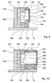
- FIG. 3 Another embodiment of a housing 46 of the receiving unit 22 is shown in a perspective view in FIG FIG. 3 shown.
- a bottom surface 48 of the housing 46 on the circuit board 18th attached.
- the housing 46 also includes an in FIG. 4 illustrated as a signal surface 50 trained side surface.
- the housing 46 is provided with two recesses 52, 54, each comprising a soldering surface 56 and 58, respectively.
- the solder surfaces 56, 58 are each coated with a solder alloy, which is shown schematically by hatching.
- the housing 46 also has a recess 60 in which a in FIG. 4 illustrated diode chip 62 is arranged in the assembled state of the receiving unit 22.
- the receiving unit 22 to the housing 46 is mounted in its assembled state and on the circuit board 18 in a partial sectional view in FIG. 4 shown.
- the housing 46 has four material layers 64, 66, 68, 70 which are stacked in a laminating direction 72.
- the material layers 64, 66, 68, 70 are made of ceramic.
- the diode chip 62 is arranged, which is soldered at an interface 74.
- the diode chip 62 is electrically connected to the interface 74 via the solder connection.
- the diode chip 62 is also electrically connected to an interface 78 via a bonding wire 76 which is soldered to the diode chip 62 on the one hand and to the interface 78 on the other hand.
- solder alloy For soldering the diode chip 62 and the bonding wire 76, the interface 74 and 78, a solder alloy.
- This solder alloy is as in FIG. 5 shown in detail, in contact with the soldering surface 56 and 58, respectively, so that an electrical connection between the interface 74 and 78 and the soldering surface 56 or 58 is made.
- the diode chip 62 is electrically connected to the printed circuit board 18 via the interface 74 and the soldering surface 56 at a first layer level on the one hand and via the interface 78 and the soldering surface 58 at a second layer level to the printed circuit board 18 on the other.
- the depression 60 is insulated from the outside by a glass ceiling 80 which forms the signal surface 50.
- the housing 46 can be made of a one-piece plastic part, which is provided with a stamped grid.
- the housing 46 has material layers that are stacked in a laminating direction at a plurality of layer levels, wherein the Auf fürraum is aligned parallel to one of the grid axes. Adjacent material layers at two different layer levels and / or within a layer level may abut each other with an interface, with an interface formed by interfaces of elementary grid cells.
- the stamped grid is preferably made of a conductive material so that an internal electrical connection in the housing 46 and an electrical connection with a soldering surface for soldering the housing 46 to the printed circuit board 18 can be made via the stamped grid.
- FIG. 5 2 shows a further sectional view of the housing 46.
- the material layers 64, 66, 68, 70 and the recess 52 with the soldering surface 56 can be seen.
- the interface 74 on which the diode chip 62 is soldered (FIG. FIG. 4 ), is coated with a solder alloy which is continuous under the material layer 66 up to a contact point 81 with the soldering surface 56.
- FIG. 6 shows the arrangement of the receiving unit 22 with the housing 46 on the circuit board 18 in a plan view.
- FIG. 7 An alternative embodiment of a housing 82 of the receiving unit 22 is shown in FIG FIG. 7 shown in a perspective view.
- the following description is limited to the differences in the structure of the housings 46 and 82.
- the housing 82 has three recesses 84, 86, 88, each comprising a soldering surface 90, 92, 94 for soldering the bottom surface 48 to the circuit board 18.
- a ground connection of the diode chip 62 to the printed circuit board 18 is produced via an interface 95 on a third layer level lying deeper in the laminating direction 72, which is electrically connected to the diode chip 62 on the one hand and the soldering surface 92 on the other hand.
- the soldering surface 92 of the interface 78 on the one hand and the solder pads 90, 94 bounded by the interface 74 on the other hand in the laminating direction 72 In order to achieve an effective electrical insulation between the underlying layer level and the upper layer levels, the soldering surface 92 of the interface 78 on the one hand and the solder pads 90, 94 bounded by the interface 74 on the other hand in the laminating direction 72.
- FIG. 8 the receiving unit 22 with a further embodiment of a housing 96 is shown schematically.
- This has a signal surface 98, which is permeable to a measurement signal received by a diode chip 100, and a bottom surface 102, which is soldered to the printed circuit board 18 is.
- the housing 96 comprises different outer surfaces 104, 106, 108, 110 from the bottom surface 102 and the signal surface 98.
- the bottom surface 102 and the outer surfaces 104, 106, 108, 110 are provided with fastening means 112, 114, 116, 118, which are designed as solder surfaces. 120, 124, 126, 128 provided.
- one of the outer surfaces 104, 106, 108, 110 can be soldered to the printed circuit board 18 by means of one of the fastening means 112, 114, 116, 118, 120, 124, whereby a different orientation of a measurement signal generated by the diode chip 100 relative can be achieved to the circuit board 18.
- the transmitting unit 20 and the receiving unit 22 are identical both in their construction and in the manner in which they are fastened to the printed circuit board 18. For corresponding parts of the transmitting unit 20 and the receiving unit 22 no new reference numerals are given.
- FIG. 9 an alternative embodiment of a housing 130 of the receiving unit 22 is shown in a sectional view.
- the housing 130 which has a plurality of material layers 132, 134, 136, 138, is soldered to the circuit board 18 with a bottom surface 140.
- a side surface of the housing 130 is formed as a signal surface 142 and is formed by a permeable to the receiving measurement signal glass ceiling 144.
- the glass ceiling 144 is omitted or that the signal surface 142 is formed by a potting compound.
- a diode chip 146 is soldered to an interface 148. As above for the receiving unit 22 on the basis of FIG.
- the diode chip 146 with the interface 148 on the one hand and on a bonding wire 150 is electrically connected to an interface 152.
- the boundary surfaces 148, 152 are each electrically connected to soldering surfaces of the housing 130, not shown in the figure, via which the housing 130 is soldered to the printed circuit board 18.
- the diode chip 146 is electrically connected to the printed circuit board 18.
- a received measurement signal in the form of a light beam 153 with a parallax angle relative to the printed circuit board 18 can fall onto the signal surface 142.
- the receiving unit 22 is provided with a deflection means 154. This is formed by an extension of the material layer 138, which is optionally coated with a Reflektierstoff.
- FIG. 10 an embodiment of the receiving unit 22 is shown. This has a deflection means 156, which is arranged in the housing 130.
- the transmitting unit 20 is constructed in the manner and attached to the circuit board 18 described above for the receiving unit 22.
Landscapes
- Engineering & Computer Science (AREA)
- Physics & Mathematics (AREA)
- Computer Networks & Wireless Communication (AREA)
- General Physics & Mathematics (AREA)
- Radar, Positioning & Navigation (AREA)
- Remote Sensing (AREA)
- Electromagnetism (AREA)
- Optical Radar Systems And Details Thereof (AREA)
Abstract
Claims (10)
- Appareil de mesure de distance, en particulier appareil de mesure de distance (10) par laser, configuré comme appareil manuel, présentant
une carte de circuit (18),
une unité d'émission et une unité de réception (20, 22) qui servent à émettre ou recevoir un signal de mesure et un boîtier (30, 46, 82, 96, 130) dont une surface de fond (32, 48, 102, 140) est tournée vers la carte de circuit (18),
une surface latérale et une surface de signal (38, 50, 98, 142), la surface de signal étant une surface disposée dans un parcours de signal de mesure, la surface latérale étant configurée comme surface de signal (38, 50, 98, 142),
caractérisé en ce que
l'unité de réception (22) présente un moyen de déviation (154, 156) qui dévie le signal de mesure et qui est disposé dans le boîtier (130) de telle sorte qu'un faisceau lumineux (153) incident sur la surface de signal (142) sous un angle de parallaxe en provenance du voisinage de l'appareil de mesure de distance est dévié sur le récepteur. - Appareil de mesure de distance selon la revendication 1, caractérisé en ce que le boîtier (46, 82, 130) présente au moins deux couches de matière (64, 66, 68, 70, 132, 134, 136, 138), une liaison électrique étant établie par l'intermédiaire d'une surface frontière (74, 78, 95, 148, 152) située entre les couches de matière (64, 66, 68, 70, 132, 134, 136, 138).
- Appareil de mesure de distance selon la revendication 2, caractérisé en ce que l'unité d'émission et l'unité de réception (20, 22) présentent une puce à diode (62, 146) qui est reliée électriquement à une surface frontière (74, 78, 148, 152) sur au moins deux niveaux de couches.
- Appareil de mesure de distance selon la revendication 2 ou 3, caractérisé en ce que le boîtier (46, 82) présente une surface brasée (56, 58, 90, 92, 94) reliée électriquement à une surface frontière (74, 78, 95).
- Appareil de mesure de distance selon la revendication 4, caractérisé en ce que la surface brasée (90, 92, 94) est délimitée par une surface frontière (74, 78) dans la direction de stratification (72).
- Appareil de mesure de distance selon l'une des revendications précédentes, caractérisé en ce que le boîtier (46, 82) présente une découpe (52, 54, 84, 86, 88) dotée d'une surface brasée (56, 58, 90, 92, 94).
- Appareil de mesure de distance selon l'une des revendications précédentes, caractérisé en ce que l'unité d'émission et l'unité de réception (20, 22) présentent un moyen de fixation (112, 114, 116, 118, 120, 124) qui est prévu pour fixer sur la carte de circuit (18) une surface extérieure (104, 106, 108, 110) différente de la surface de fond (102) et de la surface de signal (98).
- Appareil de mesure de distance selon la revendication 7, caractérisé en ce que le boîtier (96) présente au moins deux moyens de fixation (112, 114, 116, 118, 120, 124) configurés comme surfaces brasées et disposés sur deux surfaces extérieures (104, 106, 108, 110) adjacentes l'une à l'autre.
- Appareil de mesure de distance selon l'une des revendications précédentes, caractérisé en ce que l'unité d'émission et l'unité de réception (20, 22) présentent un moyen de déviation (154, 156) qui dévie le signal de mesure et qui est disposé dans le boîtier (130).
- Appareil de mesure de distance selon la revendication 9, caractérisé en ce que le moyen de déviation (154) est formé d'un seul tenant avec le boîtier (130).
Applications Claiming Priority (2)
| Application Number | Priority Date | Filing Date | Title |
|---|---|---|---|
| DE102005035101A DE102005035101A1 (de) | 2005-07-27 | 2005-07-27 | Entfernungsmessgerät |
| PCT/EP2006/063464 WO2007012526A1 (fr) | 2005-07-27 | 2006-06-22 | Appareil de telemetrie |
Publications (2)
| Publication Number | Publication Date |
|---|---|
| EP1910861A1 EP1910861A1 (fr) | 2008-04-16 |
| EP1910861B1 true EP1910861B1 (fr) | 2012-05-30 |
Family
ID=36954542
Family Applications (1)
| Application Number | Title | Priority Date | Filing Date |
|---|---|---|---|
| EP06763857A Not-in-force EP1910861B1 (fr) | 2005-07-27 | 2006-06-22 | Appareil de telemetrie |
Country Status (6)
| Country | Link |
|---|---|
| US (1) | US7843553B2 (fr) |
| EP (1) | EP1910861B1 (fr) |
| JP (1) | JP2009503475A (fr) |
| CN (1) | CN101233422A (fr) |
| DE (1) | DE102005035101A1 (fr) |
| WO (1) | WO2007012526A1 (fr) |
Families Citing this family (1)
| Publication number | Priority date | Publication date | Assignee | Title |
|---|---|---|---|---|
| DE102017205195A1 (de) * | 2016-07-28 | 2018-02-01 | Robert Bosch Gmbh | Laserentfernungsmessgerät |
Family Cites Families (3)
| Publication number | Priority date | Publication date | Assignee | Title |
|---|---|---|---|---|
| US6888169B2 (en) * | 2000-09-29 | 2005-05-03 | Optical Communication Products, Inc. | High speed optical subassembly with ceramic carrier |
| DE50213215D1 (de) * | 2002-03-18 | 2009-03-05 | Hilti Ag | Elektrooptisches para-axiales Distanzmesssystem |
| US7394528B2 (en) * | 2005-03-25 | 2008-07-01 | Neverguess Rangefinders, Inc. | User-worn rangefinder system and methods |
-
2005
- 2005-07-27 DE DE102005035101A patent/DE102005035101A1/de not_active Withdrawn
-
2006
- 2006-06-22 EP EP06763857A patent/EP1910861B1/fr not_active Not-in-force
- 2006-06-22 JP JP2008523283A patent/JP2009503475A/ja not_active Withdrawn
- 2006-06-22 WO PCT/EP2006/063464 patent/WO2007012526A1/fr active Application Filing
- 2006-06-22 US US11/911,237 patent/US7843553B2/en not_active Expired - Fee Related
- 2006-06-22 CN CNA2006800273430A patent/CN101233422A/zh active Pending
Also Published As
| Publication number | Publication date |
|---|---|
| US7843553B2 (en) | 2010-11-30 |
| WO2007012526A1 (fr) | 2007-02-01 |
| DE102005035101A1 (de) | 2007-02-01 |
| EP1910861A1 (fr) | 2008-04-16 |
| US20080192227A1 (en) | 2008-08-14 |
| CN101233422A (zh) | 2008-07-30 |
| JP2009503475A (ja) | 2009-01-29 |
Similar Documents
| Publication | Publication Date | Title |
|---|---|---|
| EP1174745B1 (fr) | Module optoélectronique montable en surface | |
| EP2786169A1 (fr) | Télémètre | |
| EP3206386A1 (fr) | Module pour un vidéo-endoscope | |
| EP0809304A2 (fr) | Convertisseur optoélectronique et procédé de fabrication | |
| WO2008083672A2 (fr) | Boîtier pour composant optoélectronique et disposition d'un composant optoélectronique dans un boîtier | |
| DE102016119002A1 (de) | Optoelektronisches bauelement und verfahren zum herstellen eines optoelektronischen bauelements | |
| DE10004411A1 (de) | Elektrooptisches Sende-/Empfangsmodul und Verfahren zu seiner Herstellung | |
| DE19536454A1 (de) | Optoelektronisches Halbleiter-Bauelement | |
| DE2922949A1 (de) | Vorrichtung zum anschluss wenigstens einer licht emittierenden diode an einen optischen lichtleiter | |
| DE10351704B4 (de) | Optoelektronische Sende- und/oder Empfangsanordnung mit einem opto-elektronischen Wandlermodul | |
| DE19944042A1 (de) | Beleuchtungseinheit für eine Vorrichtung für Anwendungen im Bereich der Medizin | |
| EP0712161B1 (fr) | Elément semi-conducteur pour une transmission optique de données bidirectionnelle en espace libre | |
| WO2007012531A1 (fr) | Appareil de telemetrie et procede pour fixer une unite electro-optique a une unite support de conducteurs | |
| EP0712005A2 (fr) | Capteur d'accélération piézo-électrique | |
| EP3696515A1 (fr) | Module radar | |
| EP1910861B1 (fr) | Appareil de telemetrie | |
| DE60222736T2 (de) | Optisches Modul mit Monitor-Photodiode | |
| EP1958000A1 (fr) | Unite modulaire pour un systeme d'antenne radar comprenant une puce hf integree | |
| DE102017123342A1 (de) | TO-Gehäuse mit hoher Reflexionsdämpfung | |
| EP1653265B1 (fr) | Dispositif de couplage optique d'un guide d'onde avec l'unité optique d'un module optique et élément de couplage pour un tel dispositif | |
| EP0622874B1 (fr) | Arrangement de couplage entre un élément optoélectronique récepteur et un élément optoélectronique émetteur | |
| DE102021206124A1 (de) | Radarvorrichtung und Verfahren zum Herstellen einer Radarvorrichtung. | |
| DE19755806A1 (de) | Elektrooptisches Modul | |
| EP1447696B1 (fr) | Composant optoéléctronique modulaire | |
| WO2015039808A1 (fr) | Composant luminescent optoélectronique et assemblage formant châssis de conducteurs |
Legal Events
| Date | Code | Title | Description |
|---|---|---|---|
| PUAI | Public reference made under article 153(3) epc to a published international application that has entered the european phase |
Free format text: ORIGINAL CODE: 0009012 |
|
| 17P | Request for examination filed |
Effective date: 20080227 |
|
| AK | Designated contracting states |
Kind code of ref document: A1 Designated state(s): AT BE BG CH CY CZ DE DK EE ES FI FR GB GR HU IE IS IT LI LT LU LV MC NL PL PT RO SE SI SK TR |
|
| 17Q | First examination report despatched |
Effective date: 20080609 |
|
| REG | Reference to a national code |
Ref country code: DE Ref legal event code: R079 Ref document number: 502006011507 Country of ref document: DE Free format text: PREVIOUS MAIN CLASS: G01S0007481000 Ipc: G01S0017080000 |
|
| GRAP | Despatch of communication of intention to grant a patent |
Free format text: ORIGINAL CODE: EPIDOSNIGR1 |
|
| DAX | Request for extension of the european patent (deleted) | ||
| RIC1 | Information provided on ipc code assigned before grant |
Ipc: G01S 7/481 20060101ALI20120210BHEP Ipc: G01S 17/36 20060101ALI20120210BHEP Ipc: G01S 17/08 20060101AFI20120210BHEP Ipc: G01S 7/497 20060101ALI20120210BHEP |
|
| GRAS | Grant fee paid |
Free format text: ORIGINAL CODE: EPIDOSNIGR3 |
|
| GRAA | (expected) grant |
Free format text: ORIGINAL CODE: 0009210 |
|
| AK | Designated contracting states |
Kind code of ref document: B1 Designated state(s): AT BE BG CH CY CZ DE DK EE ES FI FR GB GR HU IE IS IT LI LT LU LV MC NL PL PT RO SE SI SK TR |
|
| REG | Reference to a national code |
Ref country code: GB Ref legal event code: FG4D Free format text: NOT ENGLISH |
|
| REG | Reference to a national code |
Ref country code: CH Ref legal event code: EP |
|
| REG | Reference to a national code |
Ref country code: AT Ref legal event code: REF Ref document number: 560307 Country of ref document: AT Kind code of ref document: T Effective date: 20120615 |
|
| REG | Reference to a national code |
Ref country code: IE Ref legal event code: FG4D Free format text: LANGUAGE OF EP DOCUMENT: GERMAN |
|
| REG | Reference to a national code |
Ref country code: DE Ref legal event code: R096 Ref document number: 502006011507 Country of ref document: DE Effective date: 20120726 |
|
| PGFP | Annual fee paid to national office [announced via postgrant information from national office to epo] |
Ref country code: CH Payment date: 20120622 Year of fee payment: 7 |
|
| PGFP | Annual fee paid to national office [announced via postgrant information from national office to epo] |
Ref country code: FR Payment date: 20120705 Year of fee payment: 7 Ref country code: GB Payment date: 20120621 Year of fee payment: 7 |
|
| REG | Reference to a national code |
Ref country code: NL Ref legal event code: VDEP Effective date: 20120530 |
|
| REG | Reference to a national code |
Ref country code: LT Ref legal event code: MG4D Effective date: 20120502 |
|
| PG25 | Lapsed in a contracting state [announced via postgrant information from national office to epo] |
Ref country code: LT Free format text: LAPSE BECAUSE OF FAILURE TO SUBMIT A TRANSLATION OF THE DESCRIPTION OR TO PAY THE FEE WITHIN THE PRESCRIBED TIME-LIMIT Effective date: 20120530 Ref country code: CY Free format text: LAPSE BECAUSE OF FAILURE TO SUBMIT A TRANSLATION OF THE DESCRIPTION OR TO PAY THE FEE WITHIN THE PRESCRIBED TIME-LIMIT Effective date: 20120530 Ref country code: FI Free format text: LAPSE BECAUSE OF FAILURE TO SUBMIT A TRANSLATION OF THE DESCRIPTION OR TO PAY THE FEE WITHIN THE PRESCRIBED TIME-LIMIT Effective date: 20120530 Ref country code: SE Free format text: LAPSE BECAUSE OF FAILURE TO SUBMIT A TRANSLATION OF THE DESCRIPTION OR TO PAY THE FEE WITHIN THE PRESCRIBED TIME-LIMIT Effective date: 20120530 Ref country code: IS Free format text: LAPSE BECAUSE OF FAILURE TO SUBMIT A TRANSLATION OF THE DESCRIPTION OR TO PAY THE FEE WITHIN THE PRESCRIBED TIME-LIMIT Effective date: 20120930 |
|
| PG25 | Lapsed in a contracting state [announced via postgrant information from national office to epo] |
Ref country code: GR Free format text: LAPSE BECAUSE OF FAILURE TO SUBMIT A TRANSLATION OF THE DESCRIPTION OR TO PAY THE FEE WITHIN THE PRESCRIBED TIME-LIMIT Effective date: 20120831 Ref country code: LV Free format text: LAPSE BECAUSE OF FAILURE TO SUBMIT A TRANSLATION OF THE DESCRIPTION OR TO PAY THE FEE WITHIN THE PRESCRIBED TIME-LIMIT Effective date: 20120530 Ref country code: SI Free format text: LAPSE BECAUSE OF FAILURE TO SUBMIT A TRANSLATION OF THE DESCRIPTION OR TO PAY THE FEE WITHIN THE PRESCRIBED TIME-LIMIT Effective date: 20120530 |
|
| BERE | Be: lapsed |
Owner name: ROBERT BOSCH G.M.B.H. Effective date: 20120630 |
|
| PGFP | Annual fee paid to national office [announced via postgrant information from national office to epo] |
Ref country code: DE Payment date: 20120822 Year of fee payment: 7 |
|
| PG25 | Lapsed in a contracting state [announced via postgrant information from national office to epo] |
Ref country code: NL Free format text: LAPSE BECAUSE OF FAILURE TO SUBMIT A TRANSLATION OF THE DESCRIPTION OR TO PAY THE FEE WITHIN THE PRESCRIBED TIME-LIMIT Effective date: 20120530 Ref country code: RO Free format text: LAPSE BECAUSE OF FAILURE TO SUBMIT A TRANSLATION OF THE DESCRIPTION OR TO PAY THE FEE WITHIN THE PRESCRIBED TIME-LIMIT Effective date: 20120530 Ref country code: MC Free format text: LAPSE BECAUSE OF NON-PAYMENT OF DUE FEES Effective date: 20120630 Ref country code: DK Free format text: LAPSE BECAUSE OF FAILURE TO SUBMIT A TRANSLATION OF THE DESCRIPTION OR TO PAY THE FEE WITHIN THE PRESCRIBED TIME-LIMIT Effective date: 20120530 Ref country code: SK Free format text: LAPSE BECAUSE OF FAILURE TO SUBMIT A TRANSLATION OF THE DESCRIPTION OR TO PAY THE FEE WITHIN THE PRESCRIBED TIME-LIMIT Effective date: 20120530 Ref country code: CZ Free format text: LAPSE BECAUSE OF FAILURE TO SUBMIT A TRANSLATION OF THE DESCRIPTION OR TO PAY THE FEE WITHIN THE PRESCRIBED TIME-LIMIT Effective date: 20120530 Ref country code: EE Free format text: LAPSE BECAUSE OF FAILURE TO SUBMIT A TRANSLATION OF THE DESCRIPTION OR TO PAY THE FEE WITHIN THE PRESCRIBED TIME-LIMIT Effective date: 20120530 |
|
| PG25 | Lapsed in a contracting state [announced via postgrant information from national office to epo] |
Ref country code: PT Free format text: LAPSE BECAUSE OF FAILURE TO SUBMIT A TRANSLATION OF THE DESCRIPTION OR TO PAY THE FEE WITHIN THE PRESCRIBED TIME-LIMIT Effective date: 20121001 Ref country code: PL Free format text: LAPSE BECAUSE OF FAILURE TO SUBMIT A TRANSLATION OF THE DESCRIPTION OR TO PAY THE FEE WITHIN THE PRESCRIBED TIME-LIMIT Effective date: 20120530 Ref country code: IT Free format text: LAPSE BECAUSE OF FAILURE TO SUBMIT A TRANSLATION OF THE DESCRIPTION OR TO PAY THE FEE WITHIN THE PRESCRIBED TIME-LIMIT Effective date: 20120530 |
|
| REG | Reference to a national code |
Ref country code: IE Ref legal event code: MM4A |
|
| PGFP | Annual fee paid to national office [announced via postgrant information from national office to epo] |
Ref country code: AT Payment date: 20120620 Year of fee payment: 7 |
|
| PLBE | No opposition filed within time limit |
Free format text: ORIGINAL CODE: 0009261 |
|
| STAA | Information on the status of an ep patent application or granted ep patent |
Free format text: STATUS: NO OPPOSITION FILED WITHIN TIME LIMIT |
|
| PG25 | Lapsed in a contracting state [announced via postgrant information from national office to epo] |
Ref country code: IE Free format text: LAPSE BECAUSE OF NON-PAYMENT OF DUE FEES Effective date: 20120622 Ref country code: ES Free format text: LAPSE BECAUSE OF FAILURE TO SUBMIT A TRANSLATION OF THE DESCRIPTION OR TO PAY THE FEE WITHIN THE PRESCRIBED TIME-LIMIT Effective date: 20120910 Ref country code: BE Free format text: LAPSE BECAUSE OF NON-PAYMENT OF DUE FEES Effective date: 20120630 |
|
| 26N | No opposition filed |
Effective date: 20130301 |
|
| REG | Reference to a national code |
Ref country code: DE Ref legal event code: R097 Ref document number: 502006011507 Country of ref document: DE Effective date: 20130301 |
|
| PG25 | Lapsed in a contracting state [announced via postgrant information from national office to epo] |
Ref country code: BG Free format text: LAPSE BECAUSE OF FAILURE TO SUBMIT A TRANSLATION OF THE DESCRIPTION OR TO PAY THE FEE WITHIN THE PRESCRIBED TIME-LIMIT Effective date: 20120830 |
|
| REG | Reference to a national code |
Ref country code: CH Ref legal event code: PL |
|
| REG | Reference to a national code |
Ref country code: AT Ref legal event code: MM01 Ref document number: 560307 Country of ref document: AT Kind code of ref document: T Effective date: 20130622 |
|
| GBPC | Gb: european patent ceased through non-payment of renewal fee |
Effective date: 20130622 |
|
| REG | Reference to a national code |
Ref country code: FR Ref legal event code: ST Effective date: 20140228 |
|
| REG | Reference to a national code |
Ref country code: DE Ref legal event code: R119 Ref document number: 502006011507 Country of ref document: DE Effective date: 20140101 |
|
| PG25 | Lapsed in a contracting state [announced via postgrant information from national office to epo] |
Ref country code: TR Free format text: LAPSE BECAUSE OF FAILURE TO SUBMIT A TRANSLATION OF THE DESCRIPTION OR TO PAY THE FEE WITHIN THE PRESCRIBED TIME-LIMIT Effective date: 20120530 Ref country code: GB Free format text: LAPSE BECAUSE OF NON-PAYMENT OF DUE FEES Effective date: 20130622 Ref country code: DE Free format text: LAPSE BECAUSE OF NON-PAYMENT OF DUE FEES Effective date: 20140101 Ref country code: LI Free format text: LAPSE BECAUSE OF NON-PAYMENT OF DUE FEES Effective date: 20130630 Ref country code: CH Free format text: LAPSE BECAUSE OF NON-PAYMENT OF DUE FEES Effective date: 20130630 |
|
| PG25 | Lapsed in a contracting state [announced via postgrant information from national office to epo] |
Ref country code: LU Free format text: LAPSE BECAUSE OF NON-PAYMENT OF DUE FEES Effective date: 20120622 Ref country code: FR Free format text: LAPSE BECAUSE OF NON-PAYMENT OF DUE FEES Effective date: 20130701 Ref country code: AT Free format text: LAPSE BECAUSE OF NON-PAYMENT OF DUE FEES Effective date: 20130622 |
|
| PG25 | Lapsed in a contracting state [announced via postgrant information from national office to epo] |
Ref country code: HU Free format text: LAPSE BECAUSE OF FAILURE TO SUBMIT A TRANSLATION OF THE DESCRIPTION OR TO PAY THE FEE WITHIN THE PRESCRIBED TIME-LIMIT Effective date: 20060622 |