EP1909132A1 - IC-driver circuit for an electro-optical device - Google Patents
IC-driver circuit for an electro-optical device Download PDFInfo
- Publication number
- EP1909132A1 EP1909132A1 EP08000581A EP08000581A EP1909132A1 EP 1909132 A1 EP1909132 A1 EP 1909132A1 EP 08000581 A EP08000581 A EP 08000581A EP 08000581 A EP08000581 A EP 08000581A EP 1909132 A1 EP1909132 A1 EP 1909132A1
- Authority
- EP
- European Patent Office
- Prior art keywords
- display control
- control signal
- driver
- display
- input
- Prior art date
- Legal status (The legal status is an assumption and is not a legal conclusion. Google has not performed a legal analysis and makes no representation as to the accuracy of the status listed.)
- Withdrawn
Links
- 230000007274 generation of a signal involved in cell-cell signaling Effects 0.000 claims abstract description 15
- 230000007704 transition Effects 0.000 claims description 4
- 239000004973 liquid crystal related substance Substances 0.000 abstract description 58
- 238000010586 diagram Methods 0.000 description 9
- 230000005540 biological transmission Effects 0.000 description 6
- 230000003247 decreasing effect Effects 0.000 description 5
- 230000007423 decrease Effects 0.000 description 4
- 230000006870 function Effects 0.000 description 4
- 239000011521 glass Substances 0.000 description 4
- 230000010355 oscillation Effects 0.000 description 4
- 230000003111 delayed effect Effects 0.000 description 3
- 238000009413 insulation Methods 0.000 description 3
- 230000000630 rising effect Effects 0.000 description 3
- 201000004059 subependymal giant cell astrocytoma Diseases 0.000 description 3
- 239000000758 substrate Substances 0.000 description 3
- 239000010409 thin film Substances 0.000 description 3
- 101000885321 Homo sapiens Serine/threonine-protein kinase DCLK1 Proteins 0.000 description 2
- 102100039758 Serine/threonine-protein kinase DCLK1 Human genes 0.000 description 2
- 230000012447 hatching Effects 0.000 description 2
- 241000283070 Equus zebra Species 0.000 description 1
- 230000001934 delay Effects 0.000 description 1
- 230000001419 dependent effect Effects 0.000 description 1
- 238000005401 electroluminescence Methods 0.000 description 1
- 239000007788 liquid Substances 0.000 description 1
- 239000000463 material Substances 0.000 description 1
- 239000011159 matrix material Substances 0.000 description 1
- 239000002184 metal Substances 0.000 description 1
- 238000000034 method Methods 0.000 description 1
- 238000012986 modification Methods 0.000 description 1
- 230000004048 modification Effects 0.000 description 1
- 238000003825 pressing Methods 0.000 description 1
- 238000007789 sealing Methods 0.000 description 1
- 230000001360 synchronised effect Effects 0.000 description 1
- 238000002834 transmittance Methods 0.000 description 1
Images






Classifications
-
- G—PHYSICS
- G09—EDUCATION; CRYPTOGRAPHY; DISPLAY; ADVERTISING; SEALS
- G09G—ARRANGEMENTS OR CIRCUITS FOR CONTROL OF INDICATING DEVICES USING STATIC MEANS TO PRESENT VARIABLE INFORMATION
- G09G3/00—Control arrangements or circuits, of interest only in connection with visual indicators other than cathode-ray tubes
- G09G3/20—Control arrangements or circuits, of interest only in connection with visual indicators other than cathode-ray tubes for presentation of an assembly of a number of characters, e.g. a page, by composing the assembly by combination of individual elements arranged in a matrix no fixed position being assigned to or needed to be assigned to the individual characters or partial characters
- G09G3/34—Control arrangements or circuits, of interest only in connection with visual indicators other than cathode-ray tubes for presentation of an assembly of a number of characters, e.g. a page, by composing the assembly by combination of individual elements arranged in a matrix no fixed position being assigned to or needed to be assigned to the individual characters or partial characters by control of light from an independent source
- G09G3/36—Control arrangements or circuits, of interest only in connection with visual indicators other than cathode-ray tubes for presentation of an assembly of a number of characters, e.g. a page, by composing the assembly by combination of individual elements arranged in a matrix no fixed position being assigned to or needed to be assigned to the individual characters or partial characters by control of light from an independent source using liquid crystals
-
- G—PHYSICS
- G09—EDUCATION; CRYPTOGRAPHY; DISPLAY; ADVERTISING; SEALS
- G09G—ARRANGEMENTS OR CIRCUITS FOR CONTROL OF INDICATING DEVICES USING STATIC MEANS TO PRESENT VARIABLE INFORMATION
- G09G3/00—Control arrangements or circuits, of interest only in connection with visual indicators other than cathode-ray tubes
- G09G3/20—Control arrangements or circuits, of interest only in connection with visual indicators other than cathode-ray tubes for presentation of an assembly of a number of characters, e.g. a page, by composing the assembly by combination of individual elements arranged in a matrix no fixed position being assigned to or needed to be assigned to the individual characters or partial characters
- G09G3/34—Control arrangements or circuits, of interest only in connection with visual indicators other than cathode-ray tubes for presentation of an assembly of a number of characters, e.g. a page, by composing the assembly by combination of individual elements arranged in a matrix no fixed position being assigned to or needed to be assigned to the individual characters or partial characters by control of light from an independent source
- G09G3/36—Control arrangements or circuits, of interest only in connection with visual indicators other than cathode-ray tubes for presentation of an assembly of a number of characters, e.g. a page, by composing the assembly by combination of individual elements arranged in a matrix no fixed position being assigned to or needed to be assigned to the individual characters or partial characters by control of light from an independent source using liquid crystals
- G09G3/3611—Control of matrices with row and column drivers
- G09G3/3685—Details of drivers for data electrodes
-
- G—PHYSICS
- G09—EDUCATION; CRYPTOGRAPHY; DISPLAY; ADVERTISING; SEALS
- G09G—ARRANGEMENTS OR CIRCUITS FOR CONTROL OF INDICATING DEVICES USING STATIC MEANS TO PRESENT VARIABLE INFORMATION
- G09G3/00—Control arrangements or circuits, of interest only in connection with visual indicators other than cathode-ray tubes
- G09G3/20—Control arrangements or circuits, of interest only in connection with visual indicators other than cathode-ray tubes for presentation of an assembly of a number of characters, e.g. a page, by composing the assembly by combination of individual elements arranged in a matrix no fixed position being assigned to or needed to be assigned to the individual characters or partial characters
- G09G3/34—Control arrangements or circuits, of interest only in connection with visual indicators other than cathode-ray tubes for presentation of an assembly of a number of characters, e.g. a page, by composing the assembly by combination of individual elements arranged in a matrix no fixed position being assigned to or needed to be assigned to the individual characters or partial characters by control of light from an independent source
- G09G3/36—Control arrangements or circuits, of interest only in connection with visual indicators other than cathode-ray tubes for presentation of an assembly of a number of characters, e.g. a page, by composing the assembly by combination of individual elements arranged in a matrix no fixed position being assigned to or needed to be assigned to the individual characters or partial characters by control of light from an independent source using liquid crystals
- G09G3/3611—Control of matrices with row and column drivers
- G09G3/3648—Control of matrices with row and column drivers using an active matrix
- G09G3/3666—Control of matrices with row and column drivers using an active matrix with the matrix divided into sections
-
- G—PHYSICS
- G09—EDUCATION; CRYPTOGRAPHY; DISPLAY; ADVERTISING; SEALS
- G09G—ARRANGEMENTS OR CIRCUITS FOR CONTROL OF INDICATING DEVICES USING STATIC MEANS TO PRESENT VARIABLE INFORMATION
- G09G2310/00—Command of the display device
- G09G2310/02—Addressing, scanning or driving the display screen or processing steps related thereto
- G09G2310/0202—Addressing of scan or signal lines
- G09G2310/0221—Addressing of scan or signal lines with use of split matrices
-
- G—PHYSICS
- G09—EDUCATION; CRYPTOGRAPHY; DISPLAY; ADVERTISING; SEALS
- G09G—ARRANGEMENTS OR CIRCUITS FOR CONTROL OF INDICATING DEVICES USING STATIC MEANS TO PRESENT VARIABLE INFORMATION
- G09G2320/00—Control of display operating conditions
- G09G2320/02—Improving the quality of display appearance
- G09G2320/0233—Improving the luminance or brightness uniformity across the screen
-
- G—PHYSICS
- G09—EDUCATION; CRYPTOGRAPHY; DISPLAY; ADVERTISING; SEALS
- G09G—ARRANGEMENTS OR CIRCUITS FOR CONTROL OF INDICATING DEVICES USING STATIC MEANS TO PRESENT VARIABLE INFORMATION
- G09G3/00—Control arrangements or circuits, of interest only in connection with visual indicators other than cathode-ray tubes
- G09G3/20—Control arrangements or circuits, of interest only in connection with visual indicators other than cathode-ray tubes for presentation of an assembly of a number of characters, e.g. a page, by composing the assembly by combination of individual elements arranged in a matrix no fixed position being assigned to or needed to be assigned to the individual characters or partial characters
- G09G3/2007—Display of intermediate tones
- G09G3/2014—Display of intermediate tones by modulation of the duration of a single pulse during which the logic level remains constant
-
- G—PHYSICS
- G09—EDUCATION; CRYPTOGRAPHY; DISPLAY; ADVERTISING; SEALS
- G09G—ARRANGEMENTS OR CIRCUITS FOR CONTROL OF INDICATING DEVICES USING STATIC MEANS TO PRESENT VARIABLE INFORMATION
- G09G3/00—Control arrangements or circuits, of interest only in connection with visual indicators other than cathode-ray tubes
- G09G3/20—Control arrangements or circuits, of interest only in connection with visual indicators other than cathode-ray tubes for presentation of an assembly of a number of characters, e.g. a page, by composing the assembly by combination of individual elements arranged in a matrix no fixed position being assigned to or needed to be assigned to the individual characters or partial characters
- G09G3/34—Control arrangements or circuits, of interest only in connection with visual indicators other than cathode-ray tubes for presentation of an assembly of a number of characters, e.g. a page, by composing the assembly by combination of individual elements arranged in a matrix no fixed position being assigned to or needed to be assigned to the individual characters or partial characters by control of light from an independent source
- G09G3/36—Control arrangements or circuits, of interest only in connection with visual indicators other than cathode-ray tubes for presentation of an assembly of a number of characters, e.g. a page, by composing the assembly by combination of individual elements arranged in a matrix no fixed position being assigned to or needed to be assigned to the individual characters or partial characters by control of light from an independent source using liquid crystals
- G09G3/3611—Control of matrices with row and column drivers
- G09G3/3614—Control of polarity reversal in general
-
- G—PHYSICS
- G09—EDUCATION; CRYPTOGRAPHY; DISPLAY; ADVERTISING; SEALS
- G09G—ARRANGEMENTS OR CIRCUITS FOR CONTROL OF INDICATING DEVICES USING STATIC MEANS TO PRESENT VARIABLE INFORMATION
- G09G3/00—Control arrangements or circuits, of interest only in connection with visual indicators other than cathode-ray tubes
- G09G3/20—Control arrangements or circuits, of interest only in connection with visual indicators other than cathode-ray tubes for presentation of an assembly of a number of characters, e.g. a page, by composing the assembly by combination of individual elements arranged in a matrix no fixed position being assigned to or needed to be assigned to the individual characters or partial characters
- G09G3/34—Control arrangements or circuits, of interest only in connection with visual indicators other than cathode-ray tubes for presentation of an assembly of a number of characters, e.g. a page, by composing the assembly by combination of individual elements arranged in a matrix no fixed position being assigned to or needed to be assigned to the individual characters or partial characters by control of light from an independent source
- G09G3/36—Control arrangements or circuits, of interest only in connection with visual indicators other than cathode-ray tubes for presentation of an assembly of a number of characters, e.g. a page, by composing the assembly by combination of individual elements arranged in a matrix no fixed position being assigned to or needed to be assigned to the individual characters or partial characters by control of light from an independent source using liquid crystals
- G09G3/3611—Control of matrices with row and column drivers
- G09G3/3685—Details of drivers for data electrodes
- G09G3/3692—Details of drivers for data electrodes suitable for passive matrices only
Definitions
- the present invention relates to an electro-optical device using an electro-optical element such as a liquid crystal, and to an electronic apparatus and a display driver IC using the electro-optical device.
- a liquid crystal display displays a monochrome display or a gray scale display including halftone, for example.
- a liquid crystal element When a liquid crystal element is used as an electro-optical element and driven passively or actively, one of a plurality of row electrodes (Y electrodes) extending in a lateral direction is selected and data signals are supplied to a plurality of column electrodes (X electrodes) extending in a longitudinal direction simultaneously, thereby driving the liquid crystal for a line at a time.
- Y electrodes row electrodes
- X electrodes column electrodes
- the maximum number of external terminals of an IC chip is limited to the number calculated by dividing the maximum producible size (about 20 mm to 30 mm) of the IC chip by an allowable terminal pitch (about 50 ⁇ m in the case of a COG (chip on glass)).
- a liquid crystal display section 600 provided with 2N pieces of X electrodes is divided into two parts in a first direction, providing two X driver ICs 610 and 620 respectively driving N pieces of X electrodes.
- the X driver ICs 610 and 620 respectively supply data signals to N pieces of X electrodes based on commands and data from an MPU (microprocessor unit) (not shown). Display control signals are also generated in the X driver IC. It is sufficient that the display control signals are generated only in the X driver IC 610. In this time, the X driver 610 is called a master, and the X driver IC 620 to which the display control signals from the X driver IC 610 are input through wiring 640 is called a slave.
- Display control signals necessary for a Y driver 630 are also supplied from the master X driver IC 610 through wiring 650.
- luminance may differ between a left screen 600A driven by the X driver IC 610 and a right screen 600B driven by the X driver IC 620 in the liquid crystal display section 600.
- driving in the normally-white mode results in the right screen 600B being more whitish (pale) than the left screen 600A.
- the document "SED1520/21 DOT MATRIX LCD DRIVER", October 1996, SMPS Systems, Inc., San Jose, CA, USA describes an electro-optical device comprising: a display section that includes a plurality of first electrodes extending in a first direction, a plurality of second electrodes extending in a second direction crossing the first direction, and electro-optical elements driven by the first and second electrodes; a first driver adapted to drive the first electrodes; and a second driver adapted to drive the second electrodes.
- the first driver has a master IC for driving a first group of the first electrodes, and at least one slave IC for driving a second group of the first electrodes.
- the master IC has an oscillation circuit adapted to generate a display control signal based on a signal from an external MPU, and an output terminal adapted to output the display control signal from oscillation circuit.
- the at least one slave IC has an input terminal for receiving the display control signal output from the oscillation circuit of the master IC through an external wiring.
- the master IC has an input terminal connected via an external resistor to the output terminal to control the frequency of the oscillation circuit.
- An objective of the present invention is to provide an electro-optical device capable of decreasing the luminance difference in a screen even if a plurality of driver ICs are used to supply data signals electrodes, and an electronic apparatus and display driver IC using the electro-optical device.
- the luminance difference in the conventional art is caused by a large difference in the delay of the display control signals between the master IC and the slave IC. This is because the master IC uses the display control signal generated therein, whereas the slave IC uses the display control signal input through an external wiring.
- the difference in the delay of the display control signals causes a difference between the voltages applied to the electrodes of the display sections of the left screen 600A and the right screen 600B in Figure 10 , thereby causing the luminance difference.
- the display control signal generated in the master IC is delayed in an internal delay circuit whereas the display control signals delayed in an external wiring is used in the slave IC, thereby decreasing the difference in the delay between the display control signals used in the master IC and that used in the slave IC. This reduces the luminance difference in a screen.
- the delay in the internal delay circuit is variable, the delay can be adjusted in accordance with the signal delay depending on the external wiring to the slave IC.
- an electronic apparatus using the electro-optical device according to the above invention.
- a display driver IC used for the X driver of the above electro-optical device.
- Figures 1 to 7 show a first example of a liquid crystal device.
- FIG. 1 is a cross section schematically showing a liquid crystal device as a display unit of a portable telephone.
- the liquid crystal device has a liquid crystal module 20 provided with a liquid crystal display driver IC 10, a printed circuit board 30 provided with an MPU 300, and a connector such as an elastic connection member (zebra rubber) 40 with a conductive section and an insulation section being formed alternately which is used to electrically connect the liquid crystal module 20 and the printed circuit board 30.
- a conductive section and an insulation section are alternately laminated in the elastic connection member 40 in the longitudinal direction towards the surface from the rear face in Figure 1 . Terminals of the liquid crystal module 20 and the printed circuit board 30 are electrically connected by uniformly applying pressure in the longitudinal direction of the elastic connection member 40.
- the liquid crystal module 20 has a liquid crystal display section 28 formed by sealing a liquid crystal 26 as an electro-optical element between two glass substrates 22 and 24.
- the liquid display driver IC 10 is provided on the substrate 24 as a COG (chip on glass).
- the first example is an example in which the present invention is applied to a passive drive type liquid crystal device.
- a plurality of segment electrodes (X electrodes) and a plurality of common electrodes (Y electrodes) are formed on each surface of the glass substrates 22 and 24 in the directions crossing each other (see Figure 2 ).
- the liquid crystal display section 28 displays an image by controlling the transmittance of pixels formed on each cross portion of the X and Y electrodes using the voltage applied to the X and Y electrodes.
- the present invention is not limited to the passive drive type liquid crystal device.
- the present invention may also be applied to an active drive type liquid crystal device using a two-terminal element such as an MIM (metal-insulation layer-metal) or a TFD (thin film diode), or a three-terminal element such as a TFT (thin film transistor).
- a two-terminal element such as an MIM (metal-insulation layer-metal) or a TFD (thin film diode), or a three-terminal element such as a TFT (thin film transistor).
- the liquid crystal module 20 is arranged in a portable telephone 500 so that the liquid crystal display section 28 is exposed as shown in Figure 16 .
- the portable telephone 500 has the liquid crystal display section 28, an earphone 510, a microphone 520, an operation means 530, an antenna 540, and the like.
- the MPU 300 outputs command data or display data to the liquid crystal module 20 based on the information received through the antenna 540 or the information input by operation on the operation means 530.
- Figure 2 shows the relationship between the liquid crystal display section 28 and the liquid crystal display driver IC 10.
- Two X driver ICs 10A and 10B as the liquid crystal driver IC 10 and one Y driver IC 12 are provided.
- the X driver IC 10A functions as a master IC and the X driver IC 10B functions as a slave IC by the external wiring.
- the X driver IC 10A drives the X electrode provided in a left screen 28A of the liquid crystal display section 28 shown in Figure 2
- the X driver IC 10B drives the X electrode provided in a right screen 28B.
- Command, data, and the like output from the MPU 300 are input to the X driver ICs 10A and 10B.
- the X driver IC 10A as the master outputs display control signals generated in a display control signal generation section (details will be described later) to an external wiring 200 through an output terminal 182.
- the display control signals are input to the X driver IC 10A through a first input terminal 130 and to the X driver IC 10B through the first and second input terminals 130 and 184.
- the X driver IC 10A as the master is designed to output display control signals for the Y driver IC 12 to the Y driver IC 12.
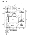
- Figure 3 shows a structure common to the X driver ICs 10A and 10B.
- the X driver ICs 10A and 10B have the following structure.
- Commands including write and read commands
- data including display data and address data
- the interface circuit 100 may have a command decoder, register, or the like.
- a display memory such as a RAM 110 has at least memory elements corresponding to the number of pixels provided in the screen 28A or 28B shown in Figure 2 .
- the display data output from the MPU 300 through the interface circuit 100 and an I/O buffer 112 is written into the RAM 110 according to the address data output from a column address circuit 114 and a row address circuit 116 based on the write command from the MPU 300.
- the MPU 300 may read out the display data written into the RAM 110.
- the display data is read out from the RAM 110 according to the address data from the column address circuit 114 and the row address circuit 116 based on the read command from the MPU 300.
- the display When the display is driven based on the display data written into the RAM 110, the display data of one line in the RAM 110 is read out and supplied to a driver 120 based on the address signal assigning one line, and output from a display address circuit 118.
- the display control signals are needed in view of the operations of the display address circuit 118 and the driver 120.
- a latch pulse LP, reset signal RES, gray scale control pulse GCP, and polar-inversion signal FR shown in Figure 4 can be given.
- These display control signals generated in a display control signal generation section 160 of the X driver 10A, as described later, are output to the outside through an input/output terminal 180 (output terminal 182 shown in Figure 6 ).
- the display control signals are then input to the X driver IC 10A through the wiring 200 and first input terminal 130 shown in Figure 2 .
- the display control signals are input to the X driver IC 10B as the slave through the wiring 200, first input terminal 130, and input/output terminal 180 (input terminal 184 shown in Figure 7 ).
- the display address circuit 118 sequentially assigns one-line read-out addresses synchronously with the latch pulse LP.
- FIG. 5 is a block diagram showing the driver 120.
- the driver 120 has a latch circuit 121, a counter 122, a coincidence-detecting circuit 123, a level shifter 124, and an LCD driver 125.
- the latch circuit 121 latches the one-line display data read out according to the addresses output from the display address circuit 118 synchronously with the latch pulse LP shown in Figure 4 .
- the counter 122 When determining four gray scale values as shown in Figure 4 , the counter 122 is reset by the reset signal RES, and counts the reset signal RES as the first count value and the gray scale control pulse GCP as the second to fourth count values.
- the coincidence-detecting circuit 123 changes its output from “L” (low) to “H” (high) or from “H” to “L” based on the logic of the polar-inversion signal FR.
- Figure 4 shows segment data SEG (00) to SEG (11) corresponding to four gray scale values during positive polar driving and negative polar driving in the case of performing polar inversion for each line. Since the effective value of the voltage applied to the liquid crystal of the pixels driven based on the segment data SEG(00) becomes a minimum, the pixels are displayed as white in the normally-white mode driving. Similarly, the pixels are displayed as half tone in the case of the segment data SEG(01) and SEG (10), and as black in the case of the segment data SEG (11).
- the level shifter 124 shifts the output level of the coincidence-detecting circuit 123.
- the voltage required for driving the liquid crystal is supplied to the segment electrodes (X electrodes) by the LCD driver 125 based on the voltage supplied from a display power source 126.
- signals YSCL and YDATA are input to the Y driver IC 12 from the master X driver IC 10A.
- the signal YSCL is synchronized with one horizontal scanning period (selection period) shown in Figure 4
- the signal YDATA is data indicating the top of one line.
- COMn and COMn+1 shown in Figure 4 show the waveforms of the signals supplied to nth and (n+1)th common electrodes (Y electrodes) shown in Figure 2 through the Y driver IC 12.
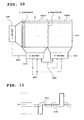
- Figures 11 and 12 show a drive waveform SEG supplied to the X electrodes from the X driver IC 10A or 10B and a drive waveform COM supplied to the Y electrodes from the Y driver IC 12.
- Figure 11 shows the drive waveform SEG for the segment electrodes (X electrodes) and the drive waveform COM for the common electrodes (Y electrodes), which are used for principle driving in a passive drive type liquid crystal device.
- the drive waveforms SEG and COM have five values of positive and negative voltage levels including a middle voltage 0 V, and COM-SEG is a voltage applied to both ends of the liquid crystal.
- Figure 12 shows the drive waveform SEG for the segment electrodes (X electrodes) and the drive waveform COM for the common electrodes (Y electrodes) which are used in other driving methods in a passive drive type liquid crystal device.
- These drive waveforms SEG and COM have six values of positive voltage levels including a minimum voltage 0 V.
- the display control signals LP, RES, GCP, and FR are generated only in the display control signal generation section 160 of the X driver IC 10A.
- Figure 6 shows part of the X driver IC 10A as the master.
- the display control signal generation section 160 has a NAND-gate 166 connected to an M/S selection terminal 162 and a dot clock input terminal 164.
- the X driver IC 10A is designed to function as the master IC by setting the M/S selection terminal 162 to "H" externally. Therefore, a dot clock DCLK input through an oscillator 163 and the dot clock input terminal 164 passes through the NAND-gate 166 and is input to a signal generator 168.
- the signal generator 168 generates the display control signals LP, RES, GCP, and FR based on the data (number of the duty sets, number of polar inversions, and the like) and command (write command) output from the interface circuit 100 and the dot clock DCLK.
- the X driver IC 10A as the master becomes equivalent to the case where the display control signal generation section 160 is enabled by setting the M/S selection terminal 162 to "H".
- the dot clock output from the dot clock input terminal 164 does not pass through the NAND-gate 166, as shown in Figure 7 . Therefore, the display control signals LP, RES, GCP, and FR are not generated in the display control signal generation section 160 of the X driver IC 10B as the slave. Specifically, the X driver IC 10B as the slave becomes equivalent to the case where the display control signal generation section 160 is disabled by setting the M/S selection terminal 162 to "L".
- the input/output terminal 180 shown in Figure 3 has the output terminal 182 and the second input terminal 184 for convenience of explanation.
- An input/output-switching circuit 170 which switches the state of the input/output terminal 180 has a transmission gate 172 driven by the logic of the M/S selection terminal 162 and an OR-gate 173 which carries out the logical OR between the signal output from the second input terminal 184 and the signal output from the M/S selection terminal 162, as shown in Figures 6 and 7 .
- the output terminal 182 is put in an output-possible state by the input/output-switching circuit 170, whereas the output of the OR-gate 173 is set to "H" regardless of the input from the second input terminal 184.
- the logic input from the second input terminal 184 is output as is from the OR gate 173 (specifically, the second input terminal 184 is put in an input-possible state), whereas the output terminal 182 is set to a high-impedance state (output-impossible state).
- the X driver IC 10A as the master generates the display signals LP, RES, GCP, and RF, and each signal is not used as is in the IC 10A but output through the output terminal 182.
- an AND-gate 140 shown in Figures 6 and 7 constitutes a signal selection circuit 140 shown in Figure 3 .
- the AND-gate 140 carries out the logical AND between the display control signals input through the first input terminal 130 and the second input terminal 184.
- the second input terminal 184 is in an input-possible state, as shown in Figure 7 . Therefore, the display control signals are supplied from the first and second input terminals 130 and 184 to the AND-gate 140, where the logical AND between the display control signals is carried out. The display control signals are then supplied to the display address circuit 118 and the driver 120 through the signal supply section 150.
- the delay of the display control signals in a X driver IC 610 as the master is caused by the resistance and capacity of the internal wiring
- the delay of the display control signal in a X driver IC 620 as the slave is caused by the resistance and capacity of an external wiring 640 in addition to those of the internal wiring.
- the delay of the display control signals used in the X driver IC 620 as the slave is larger than the delay of the display control signals used in the X driver IC 610 as the master.
- Figure 8 shows a gray scale control pulse GCP generated during one horizontal scanning period (selection period) and a signal SEG(00) obtained by the pulse GCP in each of the X driver ICs 610 and 620 of the liquid crystal device of the conventional art shown in Figure 10 .
- the delay of a gray scale control pulse GCPA is small, whereas the delay of a gray scale control pulse GCPB is large in the X driver IC 620.
- the rising edges of the signals SEGA(00) and SEGB(00) generated in the X driver ICs 610 and 620 are determined by the fall timings t1 and t2 of the corresponding gray scale control pulses GCPA and GCPB, respectively. Therefore, the rise timing t2 of the signal SEGB(00) is later than the rise timing t1 of the signal SEGA(00).
- the length of one horizontal scanning period is determined by the signal COMn supplied to the nth Y electrode from the Y driver IC 630, for example.
- the signal COMn is used as a signal common to both signals SEG output from both X driver ICs 610 and 620. Therefore, the start time t0 and end time t3 of one horizontal scanning period (selection period) are common to both signals SEG.
- the gray scale value of the signal SEGA (00) generated in the X driver IC 610 is set based on the effective value defined by the product of the time from t1 to t3 by a voltage (area S1 shown by hatching).
- the gray scale value of the signal SEGB (00) generated in the X driver IC 620 is set based on the effective value defined by the product of the time from t2 to t3 by a voltage (area S2 shown by hatching).
- the luminance difference in the conventional art shown in Figure 10 can be decreased to such an extent that the difference is not significant visually. The reason will be described below.
- L1 L2 ⁇ L3.
- the gray scale control pulses input to the first input terminal 130 of the X driver IC 10A and the first and second input terminals 130 and 184 of the X driver 10B are respectively referred to as GCPA, GCPB1, and GCPB2, as shown in Figure 9 .
- the effective value of the voltage applied to the liquid crystal of the pixels depends on the rise timing of the gray scale control pulses GCPA, GCPB1, and GCPB2, as shown in Figure 9 . Therefore, use of the gray scale control pulse GCPB1 having the same rise timing as that of the gray scale control pulse GCPA used in the X driver 10A is sufficient.
- the AND-gate 140 is used as the selection circuit 140 shown in Figure 3 , where the logical AND between the gray scale control pulses GCPB1 and GCPB2 is carried out as shown in Figure 9 , thereby selecting the rising edge of the gray scale control pulse GCPB1.
- the lengths L1 and L2 of the wiring 200 shown in Figure 3 may be equal or the difference between the two lengths may be decreased.
- the difference in wiring delay may be decreased by changing the width or materials of the wiring 200 in each region.
- the signal selection circuit 140 which selects the logic transition state of one of two display control signals differing in delay, which are respectively input from the first and second input terminals 130 and 184, is not limited to an AND-gate.
- the signal selection circuit 140 may be a switch which selects one of the gray scale control pulses GCPB1 and GCPB2 shown in Figure 9 .
- An OR-gate may be used as the signal selection circuit in order to select the falling edge of the gray scale control pulse GCPB2 in Figure 9 .
- the signal selection circuit may be structured so that the transition state of necessary logic can be selected.
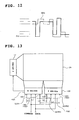
- Figure 13 shows a second example of the present invention in which the wiring 200 for the X driver ICs 10A and 10B differs from that in Figure 2 .
- the lengths of each region of the wiring 200 satisfy L2 ⁇ L1 ⁇ L3 and L3 - L1 ⁇ L1 - L2. Therefore, in the case of the wiring example shown in Figure 13 , the gray scale control pulses GCPA, GCPB1, and GCPB2 become as shown in Figure 14 .
- the gray scale control pulse GCPB2 having fall timing close to that of the gray scale control pulse GCPA used in the X driver 10A may be used.
- an OR-gate may be used as the selection circuit 140 shown in Figure 3 , where the logical OR between the gray scale control pulses GCPB1 and GCPB2 is carried out, thereby selecting the falling edge of the gray scale control pulse GCPB2 as shown in Figure 14 .
- Figure 15 shows an example in which three X driver ICs 10A, 10B, and 10C are connected.
- the center X driver IC 10A may be the master and both the X driver ICs 10B and 10C adjacent to the X driver IC 10A may be the slaves.
- the difference in the time of the falling edge between, for example, the gray scale control pulses GCP used in each of these X driver ICs 10A, 10B, and 10C becomes smaller by selecting the display control signal (including GCPB2) output from a second input terminal 184 for the X driver IC 10B and the display control signal (including GCPB1) output from the first input terminal 130 for the X driver IC 10C. This decreases the luminance difference in a screen.
- an AND-gate which carries out the logical AND between the display control signals differing in delay which are output from the first and second input terminals 130 and 184 may be used as the signal selection circuit 140 in the X driver IC 10B.
- an OR-gate may be used as the signal selection circuit 140.
- an AND-gate and an OR-gate may be provided to the signal selection circuit 140 so that either one of these gates or the outputs of the gates is selected by providing an external wiring.
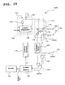
- Figure 17 shows a liquid crystal device according to an embodiment of the present invention.
- display control signals output from an input/output terminal 180 (output terminal 182) of an X driver IC 400A as a master are input to an X driver IC 400B as a slave through a first input terminal 130 and a second input terminal 184 (input/output terminal 180) of the X driver 400B.
- Figures 18 and 19 show block diagrams of part of the X driver ICs 400A and 400B shown in Figure 17 . Parts having the same function as those in the block diagrams shown in Figures 6 and 7 are represented by the same symbols, and description thereof will be omitted.
- the X driver IC 400A shown in Figure 18 and the X driver IC 400B shown in Figure 19 have the same structure, and differ in their function by the logic input to an M/S selection terminal 162.
- driver ICs 400A and 400B differ from those shown in Figures 6 and 7 in that the internal structure of an input/output-switching circuit 410 is different, an internal delay circuit 420 is provided, and an AND-gate 430 and an OR-gate 440 are provided as the signal selection circuits.
- the input/output-switching circuit 410 has a second transmission gate 174 which is in a state capable of inputting the input signal output from a second input terminal 184 based on an "H" output from an inverter 176, which inverses the input logic from the M/S selection terminal 162 when a transmission gate 172 to be connected to an output terminal 182 is designated as a first transmission gate.
- the input/output-switching circuit 410 has a path which serves to input the display control signal output from a signal generator 168 to the internal delay circuit 420, and a third transmission gate 178 which is turned on by "H" output from the M/S selection terminal 162 in the middle of the path.
- the display control signals from the signal generator 168 are input to the output terminal 182 and the internal delay circuit 420 in the X driver IC 400A as the master.
- the display control signals are input through the second input terminal 184 in the same manner as in the case shown in Figure 7 .
- the internal delay circuit 420 serves to delay the display control signals to the same extent as or close to the wiring delay of wiring 450 extending from the output terminal 182 of the X driver IC 400A to the first input terminal 130 of the X driver IC 400B. Therefore, the display control signals (including GCPA) delayed by the internal delay circuit 420 are input to a signal supply section 150 of the X driver IC 400A as the master through the OR-gate 440.
- the display control signals (including GCPB1) with a small delay and the display control signals (including GCPB2) with a large delay are input to the X driver IC 400B as the slave through the first input terminal 130 and the second input terminal 184, respectively.
- the AND-gate 430 carries out the logical AND of between these signals. Therefore, taking the gray scale control pulse GCP as an example, the falling edge of the gray scale control pulse GCPB1 with a small delay is selected. Because the third transmission gate 178 is controlled so that the output of the internal delay circuit 420 is "L", signals from the AND-gate 430 are input to the signal supply section 150 through the OR-gate 440. This enables display control using a signal with almost the same delay as that of the gray scale control pulse GCPA used in the X driver IC 400A. Therefore, the problem of the luminance difference in a screen can be solved.
- the AND-gate 430 shown in Figures 18 and 19 may be changed to an OR-gate or to a switch corresponding to the signal to be selected in the same manner as the signal selection circuit 140 in the first example.
- the signal delay in the internal delay circuit 420 is preferably variable.
- a type which can control the delay so that the luminance difference in a screen is minimized while displaying an image on the screen is still more preferable.
- the liquid crystal display when applying the present invention to a liquid crystal device, is not limited to a passive drive type liquid crystal device but may be an active drive type liquid crystal device.
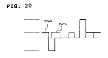
- Figure 20 shows a data signal (DATA) and a scanning signal (SCAN) used for gray scale display in the case of using a TFD as an active element.
- the electro-optical device of the present invention is not limited to those using a liquid crystal as the electro-optical element.
- the electro-optical device can be applied to those using an EI (electroluminescence) or an MMD (micro-mirror device).
- the present invention is not limited to the above types which give gray scale display using an electro-optical device.
- the present invention can be applied to types which use a binary display such as a black and white display.
- the display control signals do not include the gray scale control pulse GCP.
- a luminance difference in a screen is likewise caused.
- the luminance difference can be eliminated by applying the present invention.
- the X driver ICs used in the above embodiment have the input/output terminal 180.
- the input/output terminal 180 may be an output terminal.
- the display control signals are eventually input from only the first input terminal 130.
- use of the input/output terminal 180 is preferable inasmuch as there is the freedom of selecting one of the display control signals which are input from the first and second input terminals and differ in delay in slave ICs 10B, 10C, and 400B.
- the present invention can be applied to various electronic apparatuses using an electro-optical device such as a liquid crystal device.
- electro-optical device such as a liquid crystal device.
- electronic apparatuses include personal computers, mobile computers, word processors, pagers, televisions, view finder type or monitor direct viewing type of recording devices, electronic notebooks, portable calculators, game machines, projectors, navigation devices, and terminals for point of sales (POS) system.
- POS point of sales
Landscapes
- Engineering & Computer Science (AREA)
- Chemical & Material Sciences (AREA)
- Crystallography & Structural Chemistry (AREA)
- Physics & Mathematics (AREA)
- Computer Hardware Design (AREA)
- General Physics & Mathematics (AREA)
- Theoretical Computer Science (AREA)
- Control Of Indicators Other Than Cathode Ray Tubes (AREA)
- Liquid Crystal Display Device Control (AREA)
- Liquid Crystal (AREA)
- Devices For Indicating Variable Information By Combining Individual Elements (AREA)
Abstract
Description
- The present invention relates to an electro-optical device using an electro-optical element such as a liquid crystal, and to an electronic apparatus and a display driver IC using the electro-optical device.
- A liquid crystal display displays a monochrome display or a gray scale display including halftone, for example.
- When a liquid crystal element is used as an electro-optical element and driven passively or actively, one of a plurality of row electrodes (Y electrodes) extending in a lateral direction is selected and data signals are supplied to a plurality of column electrodes (X electrodes) extending in a longitudinal direction simultaneously, thereby driving the liquid crystal for a line at a time.
- In recent years, there has been a tendency to increase the number of X electrodes to provide an extremely fine display.
- In this case, it is difficult to drive all X electrodes using a single driver IC. This is because the maximum number of external terminals of an IC chip is limited to the number calculated by dividing the maximum producible size (about 20 mm to 30 mm) of the IC chip by an allowable terminal pitch (about 50 µm in the case of a COG (chip on glass)).
- To deal with this problem, as shown in
Figure 10 , a liquidcrystal display section 600 provided with 2N pieces of X electrodes is divided into two parts in a first direction, providing twoX driver ICs - The
X driver ICs X driver 610 is called a master, and the X driver IC 620 to which the display control signals from the X driver IC 610 are input throughwiring 640 is called a slave. - Display control signals necessary for a
Y driver 630 are also supplied from the master X driver IC 610 throughwiring 650. - In the liquid crystal display shown in
Figure 10 , luminance may differ between aleft screen 600A driven by theX driver IC 610 and aright screen 600B driven by theX driver IC 620 in the liquidcrystal display section 600. Specifically, driving in the normally-white mode results in theright screen 600B being more whitish (pale) than theleft screen 600A. - The document "SED1520/21 DOT MATRIX LCD DRIVER", October 1996, SMPS Systems, Inc., San Jose, CA, USA describes an electro-optical device comprising: a display section that includes a plurality of first electrodes extending in a first direction, a plurality of second electrodes extending in a second direction crossing the first direction, and electro-optical elements driven by the first and second electrodes; a first driver adapted to drive the first electrodes; and a second driver adapted to drive the second electrodes. The first driver has a master IC for driving a first group of the first electrodes, and at least one slave IC for driving a second group of the first electrodes. The master IC has an oscillation circuit adapted to generate a display control signal based on a signal from an external MPU, and an output terminal adapted to output the display control signal from oscillation circuit. The at least one slave IC has an input terminal for receiving the display control signal output from the oscillation circuit of the master IC through an external wiring. The master IC has an input terminal connected via an external resistor to the output terminal to control the frequency of the oscillation circuit.
- An objective of the present invention is to provide an electro-optical device capable of decreasing the luminance difference in a screen even if a plurality of driver ICs are used to supply data signals electrodes, and an electronic apparatus and display driver IC using the electro-optical device.
- This object is achieved by an electro-optical device as claimed in
claim 1. Preferred embodiments of the invention are defined in the dependent claims. - The luminance difference in the conventional art is caused by a large difference in the delay of the display control signals between the master IC and the slave IC. This is because the master IC uses the display control signal generated therein, whereas the slave IC uses the display control signal input through an external wiring. The difference in the delay of the display control signals causes a difference between the voltages applied to the electrodes of the display sections of the
left screen 600A and theright screen 600B inFigure 10 , thereby causing the luminance difference. - According to an aspect of the present invention, the display control signal generated in the master IC is delayed in an internal delay circuit whereas the display control signals delayed in an external wiring is used in the slave IC, thereby decreasing the difference in the delay between the display control signals used in the master IC and that used in the slave IC. This reduces the luminance difference in a screen.
- In this case, if the delay in the internal delay circuit is variable, the delay can be adjusted in accordance with the signal delay depending on the external wiring to the slave IC.
- According to another aspect of the present invention, there is provided an electronic apparatus using the electro-optical device according to the above invention.
- According to still another aspect of the present invention, there is provided a display driver IC used for the X driver of the above electro-optical device.
-
- Figure 1
- is a cross section schematically showing a liquid crystal display according to a first example.
- Figure 2
- shows the connection between the two X driver ICs and one Y driver IC used in the liquid crystal device of
Figure 1 and a liquid crystal display section. - Figure 3
- is a block diagram showing a configuration common to the two X driver ICs shown in
Figure 2 . - Figure 4
- is a timing chart for signals generated in the X driver IC of
Figure 3 and a Y driver IC. - Figure 5
- is a block diagram of the driver of
Figure 3 . - Figure 6
- is a partial block diagram of the master X driver IC shown in
Figure 2 . - Figure 7
- is a partial block diagram of the slave X driver IC shown in
Figure 2 . - Figure 8
- is a waveform chart for describing the delay of a gray scale control pulse and an effective voltage lag caused by the delay.
- Figure 9
- is a waveform chart for describing an operation to decrease the luminance difference in a screen.
- Figure 10
- shows the connection between two X driver ICs, one Y driver IC, and a liquid crystal display section used in a conventional liquid crystal device.
- Figure 11
- shows a drive waveform used for principle driving in a passive drive type liquid crystal device.
- Figure 12
- shows another drive waveform used in a passive drive type liquid crystal device.
- Figure 13
- shows a wiring example differing from that in
Figure 2 . - Figure 14
- is a waveform chart for describing an operation to decrease the luminance difference in a screen in the case of the wiring example of
Figure 13 . - Figure 15
- is a view showing a liquid crystal device according to a second example.
- Figure 16
- is a perspective view schematically showing a portable telephone as an example of an electronic apparatus using the liquid crystal device shown in
Figure 1 . - Figure 17
- is a view showing a liquid crystal device according to an embodiment of the present invention.
- Figure 18
- is a partial block diagram of the master X driver IC shown in
Figure 17 . - Figure 19
- is a partial block diagram of the slave X driver IC shown in
Figure 17 . - Figure 20
- shows a drive waveform used in an active drive type liquid crystal device using a TFD (thin film diode) as a switching element.
- Embodiments of the present invention will be described with reference to drawings.
-
Figures 1 to 7 show a first example of a liquid crystal device. -
Figure 1 is a cross section schematically showing a liquid crystal device as a display unit of a portable telephone. As shown inFigure 1 , the liquid crystal device has aliquid crystal module 20 provided with a liquid crystaldisplay driver IC 10, a printedcircuit board 30 provided with anMPU 300, and a connector such as an elastic connection member (zebra rubber) 40 with a conductive section and an insulation section being formed alternately which is used to electrically connect theliquid crystal module 20 and the printedcircuit board 30. A conductive section and an insulation section are alternately laminated in theelastic connection member 40 in the longitudinal direction towards the surface from the rear face inFigure 1 . Terminals of theliquid crystal module 20 and the printedcircuit board 30 are electrically connected by uniformly applying pressure in the longitudinal direction of theelastic connection member 40. - The
liquid crystal module 20 has a liquidcrystal display section 28 formed by sealing aliquid crystal 26 as an electro-optical element between twoglass substrates display driver IC 10 is provided on thesubstrate 24 as a COG (chip on glass). - The first example is an example in which the present invention is applied to a passive drive type liquid crystal device. For example, a plurality of segment electrodes (X electrodes) and a plurality of common electrodes (Y electrodes) are formed on each surface of the
glass substrates Figure 2 ). The liquidcrystal display section 28 displays an image by controlling the transmittance of pixels formed on each cross portion of the X and Y electrodes using the voltage applied to the X and Y electrodes. - The present invention is not limited to the passive drive type liquid crystal device. The present invention may also be applied to an active drive type liquid crystal device using a two-terminal element such as an MIM (metal-insulation layer-metal) or a TFD (thin film diode), or a three-terminal element such as a TFT (thin film transistor).
- The
liquid crystal module 20 is arranged in aportable telephone 500 so that the liquidcrystal display section 28 is exposed as shown inFigure 16 . Theportable telephone 500 has the liquidcrystal display section 28, anearphone 510, amicrophone 520, an operation means 530, anantenna 540, and the like. TheMPU 300 outputs command data or display data to theliquid crystal module 20 based on the information received through theantenna 540 or the information input by operation on the operation means 530. -
Figure 2 shows the relationship between the liquidcrystal display section 28 and the liquid crystaldisplay driver IC 10. TwoX driver ICs crystal driver IC 10 and oneY driver IC 12 are provided. - Although these two
X driver ICs X driver IC 10A functions as a master IC and theX driver IC 10B functions as a slave IC by the external wiring. - The
X driver IC 10A drives the X electrode provided in aleft screen 28A of the liquidcrystal display section 28 shown inFigure 2 , and theX driver IC 10B drives the X electrode provided in aright screen 28B. Command, data, and the like output from theMPU 300 are input to theX driver ICs - The
X driver IC 10A as the master outputs display control signals generated in a display control signal generation section (details will be described later) to anexternal wiring 200 through anoutput terminal 182. The display control signals are input to theX driver IC 10A through afirst input terminal 130 and to theX driver IC 10B through the first andsecond input terminals X driver IC 10A as the master is designed to output display control signals for theY driver IC 12 to theY driver IC 12. -
Figure 3 shows a structure common to theX driver ICs Figure 3 , theX driver ICs - Commands (including write and read commands) and data (including display data and address data) from the
MPU 300 are input to aninterface circuit 100 in serial or parallel throughterminals interface circuit 100 may have a command decoder, register, or the like. - A display memory such as a
RAM 110 has at least memory elements corresponding to the number of pixels provided in thescreen Figure 2 . The display data output from theMPU 300 through theinterface circuit 100 and an I/O buffer 112 is written into theRAM 110 according to the address data output from acolumn address circuit 114 and arow address circuit 116 based on the write command from theMPU 300. TheMPU 300 may read out the display data written into theRAM 110. The display data is read out from theRAM 110 according to the address data from thecolumn address circuit 114 and therow address circuit 116 based on the read command from theMPU 300. - When the display is driven based on the display data written into the
RAM 110, the display data of one line in theRAM 110 is read out and supplied to adriver 120 based on the address signal assigning one line, and output from adisplay address circuit 118. - The display control signals are needed in view of the operations of the
display address circuit 118 and thedriver 120. As examples of the display control signals, a latch pulse LP, reset signal RES, gray scale control pulse GCP, and polar-inversion signal FR shown inFigure 4 can be given. These display control signals generated in a display controlsignal generation section 160 of theX driver 10A, as described later, are output to the outside through an input/output terminal 180 (output terminal 182 shown inFigure 6 ). The display control signals are then input to theX driver IC 10A through thewiring 200 andfirst input terminal 130 shown inFigure 2 . The display control signals are input to theX driver IC 10B as the slave through thewiring 200,first input terminal 130, and input/output terminal 180 (input terminal 184 shown inFigure 7 ). - The
display address circuit 118 sequentially assigns one-line read-out addresses synchronously with the latch pulse LP. -
Figure 5 is a block diagram showing thedriver 120. InFigure 5 , thedriver 120 has alatch circuit 121, acounter 122, a coincidence-detecting circuit 123, alevel shifter 124, and anLCD driver 125. - The
latch circuit 121 latches the one-line display data read out according to the addresses output from thedisplay address circuit 118 synchronously with the latch pulse LP shown inFigure 4 . - When determining four gray scale values as shown in
Figure 4 , thecounter 122 is reset by the reset signal RES, and counts the reset signal RES as the first count value and the gray scale control pulse GCP as the second to fourth count values. - When each data value of one line output from the
latch circuit 121 coincides with the count value output from thecounter 122, the coincidence-detecting circuit 123 changes its output from "L" (low) to "H" (high) or from "H" to "L" based on the logic of the polar-inversion signal FR. -
Figure 4 shows segment data SEG (00) to SEG (11) corresponding to four gray scale values during positive polar driving and negative polar driving in the case of performing polar inversion for each line. Since the effective value of the voltage applied to the liquid crystal of the pixels driven based on the segment data SEG(00) becomes a minimum, the pixels are displayed as white in the normally-white mode driving. Similarly, the pixels are displayed as half tone in the case of the segment data SEG(01) and SEG (10), and as black in the case of the segment data SEG (11). When the polar-inversion signal FR is "H", four types of the gray scale values SEG (00) to SEG (11) output from the coincidence-detecting circuit 123 change from "L" to "H" corresponding to each gray scale value at the time of falling of the reset pulse RES or gray scale control pulse GCP, as shown inFigure 4 . When the polar-inversion signal FR is "L", four types of the gray scale values SEG (00) to SEG (11) output from the coincidence-detecting circuit 123 change from "H" to "L", as shown inFigure 4 . - The
level shifter 124 shifts the output level of the coincidence-detecting circuit 123. The voltage required for driving the liquid crystal is supplied to the segment electrodes (X electrodes) by theLCD driver 125 based on the voltage supplied from adisplay power source 126. - As shown in
Figure 2 , signals YSCL and YDATA are input to theY driver IC 12 from the masterX driver IC 10A. The signal YSCL is synchronized with one horizontal scanning period (selection period) shown inFigure 4 , and the signal YDATA is data indicating the top of one line. COMn and COMn+1 shown inFigure 4 show the waveforms of the signals supplied to nth and (n+1)th common electrodes (Y electrodes) shown inFigure 2 through theY driver IC 12. -
Figures 11 and12 show a drive waveform SEG supplied to the X electrodes from theX driver IC Y driver IC 12. -
Figure 11 shows the drive waveform SEG for the segment electrodes (X electrodes) and the drive waveform COM for the common electrodes (Y electrodes), which are used for principle driving in a passive drive type liquid crystal device. The drive waveforms SEG and COM have five values of positive and negative voltage levels including a middle voltage 0 V, and COM-SEG is a voltage applied to both ends of the liquid crystal. -
Figure 12 shows the drive waveform SEG for the segment electrodes (X electrodes) and the drive waveform COM for the common electrodes (Y electrodes) which are used in other driving methods in a passive drive type liquid crystal device. These drive waveforms SEG and COM have six values of positive voltage levels including a minimum voltage 0 V. - The display control signals LP, RES, GCP, and FR are generated only in the display control
signal generation section 160 of theX driver IC 10A.Figure 6 shows part of theX driver IC 10A as the master. - As shown in
Figure 6 , the display controlsignal generation section 160 has a NAND-gate 166 connected to an M/S selection terminal 162 and a dotclock input terminal 164. TheX driver IC 10A is designed to function as the master IC by setting the M/S selection terminal 162 to "H" externally. Therefore, a dot clock DCLK input through anoscillator 163 and the dotclock input terminal 164 passes through the NAND-gate 166 and is input to asignal generator 168. Thesignal generator 168 generates the display control signals LP, RES, GCP, and FR based on the data (number of the duty sets, number of polar inversions, and the like) and command (write command) output from theinterface circuit 100 and the dot clock DCLK. In other words, theX driver IC 10A as the master becomes equivalent to the case where the display controlsignal generation section 160 is enabled by setting the M/S selection terminal 162 to "H". - In the case of the
X driver IC 10B as the slave in which the M/S selection terminal 162 is set to "L", the dot clock output from the dotclock input terminal 164 does not pass through the NAND-gate 166, as shown inFigure 7 . Therefore, the display control signals LP, RES, GCP, and FR are not generated in the display controlsignal generation section 160 of theX driver IC 10B as the slave. Specifically, theX driver IC 10B as the slave becomes equivalent to the case where the display controlsignal generation section 160 is disabled by setting the M/S selection terminal 162 to "L". - As shown in
Figures 6 and7 , the input/output terminal 180 shown inFigure 3 has theoutput terminal 182 and thesecond input terminal 184 for convenience of explanation. An input/output-switchingcircuit 170 which switches the state of the input/output terminal 180 has atransmission gate 172 driven by the logic of the M/S selection terminal 162 and an OR-gate 173 which carries out the logical OR between the signal output from thesecond input terminal 184 and the signal output from the M/S selection terminal 162, as shown inFigures 6 and7 . - By setting the M/
S selection terminal 162 to "H" in theX driver IC 10A as the master, theoutput terminal 182 is put in an output-possible state by the input/output-switchingcircuit 170, whereas the output of theOR-gate 173 is set to "H" regardless of the input from thesecond input terminal 184. - On the contrary, by setting the M/
S selection terminal 162 to "L" in theX driver IC 10B as the slave, the logic input from thesecond input terminal 184 is output as is from the OR gate 173 (specifically, thesecond input terminal 184 is put in an input-possible state), whereas theoutput terminal 182 is set to a high-impedance state (output-impossible state). - In this example, the
X driver IC 10A as the master generates the display signals LP, RES, GCP, and RF, and each signal is not used as is in theIC 10A but output through theoutput terminal 182. - Next, configuration for inputting the display control signals LP, RES, GCP, and RF, which are externally output, to the
X driver ICs Figures 6 and7 . - In this example, an AND-gate 140 shown in
Figures 6 and7 constitutes asignal selection circuit 140 shown inFigure 3 . The AND-gate 140 carries out the logical AND between the display control signals input through thefirst input terminal 130 and thesecond input terminal 184. - As shown in
Figure 6 , no display control signal is input from thesecond input terminal 184 to theX driver IC 10A set as the master IC by the M/S selection terminal 162. At this time, the logic input to the AND-gate 140 from theOR-gate 173 is set to "H". Therefore, the display control signals input from thefirst input terminal 130 are supplied as is to thedisplay address circuit 118 and thedriver 120 through asignal supply section 150 from theAND-gate 140. - In the
X driver IC 10B set as the slave IC by the M/S selection terminal 162, thesecond input terminal 184 is in an input-possible state, as shown inFigure 7 . Therefore, the display control signals are supplied from the first andsecond input terminals AND-gate 140, where the logical AND between the display control signals is carried out. The display control signals are then supplied to thedisplay address circuit 118 and thedriver 120 through thesignal supply section 150. - As shown in
Figure 10 showing a conventional art, the delay of the display control signals in aX driver IC 610 as the master is caused by the resistance and capacity of the internal wiring, whereas the delay of the display control signal in aX driver IC 620 as the slave is caused by the resistance and capacity of anexternal wiring 640 in addition to those of the internal wiring. For this reason, the delay of the display control signals used in theX driver IC 620 as the slave is larger than the delay of the display control signals used in theX driver IC 610 as the master. -
Figure 8 shows a gray scale control pulse GCP generated during one horizontal scanning period (selection period) and a signal SEG(00) obtained by the pulse GCP in each of theX driver ICs Figure 10 . - In the
X driver IC 610, the delay of a gray scale control pulse GCPA is small, whereas the delay of a gray scale control pulse GCPB is large in theX driver IC 620. - The rising edges of the signals SEGA(00) and SEGB(00) generated in the
X driver ICs - The length of one horizontal scanning period (selection period) is determined by the signal COMn supplied to the nth Y electrode from the
Y driver IC 630, for example. The signal COMn is used as a signal common to both signals SEG output from bothX driver ICs - The gray scale value of the signal SEGA (00) generated in the
X driver IC 610 is set based on the effective value defined by the product of the time from t1 to t3 by a voltage (area S1 shown by hatching). The gray scale value of the signal SEGB (00) generated in theX driver IC 620 is set based on the effective value defined by the product of the time from t2 to t3 by a voltage (area S2 shown by hatching). - However, it is clear that S1 is not equal to S2 and the gray scale values differ in each X driver though the gray scale values were originally the same. The luminance difference described relating to the conventional art shown in
Figure 10 arises for the above reason. - On the contrary, according to this example, the luminance difference in the conventional art shown in
Figure 10 can be decreased to such an extent that the difference is not significant visually. The reason will be described below. - In
Figure 2 , the length of the wiring between theoutput terminal 182 of theX driver IC 10A and theinput terminal 130 of theX driver IC 10A is referred to as L1, and the lengths of the wiring between theoutput terminal 182 and the first andsecond input terminals X driver IC 10B are referred to as L2 and L3. As is clear fromFigure 2 , L1 = L2 < L3. - According to the above relation, the gray scale control pulses input to the
first input terminal 130 of theX driver IC 10A and the first andsecond input terminals X driver 10B are respectively referred to as GCPA, GCPB1, and GCPB2, as shown inFigure 9 . - As described above, the effective value of the voltage applied to the liquid crystal of the pixels depends on the rise timing of the gray scale control pulses GCPA, GCPB1, and GCPB2, as shown in
Figure 9 . Therefore, use of the gray scale control pulse GCPB1 having the same rise timing as that of the gray scale control pulse GCPA used in theX driver 10A is sufficient. - In this example, as shown in
Figures 6 and7 , theAND-gate 140 is used as theselection circuit 140 shown inFigure 3 , where the logical AND between the gray scale control pulses GCPB1 and GCPB2 is carried out as shown inFigure 9 , thereby selecting the rising edge of the gray scale control pulse GCPB1. - This makes the delays of the display control signals respectively input to the
X driver ICs right screens Figure 1 . - The lengths L1 and L2 of the
wiring 200 shown inFigure 3 may be equal or the difference between the two lengths may be decreased. In addition, the difference in wiring delay may be decreased by changing the width or materials of thewiring 200 in each region. - Moreover, the
signal selection circuit 140 which selects the logic transition state of one of two display control signals differing in delay, which are respectively input from the first andsecond input terminals signal selection circuit 140 may be a switch which selects one of the gray scale control pulses GCPB1 and GCPB2 shown inFigure 9 . An OR-gate may be used as the signal selection circuit in order to select the falling edge of the gray scale control pulse GCPB2 inFigure 9 . There may be the case of operating synchronously with the rising edge of the display control signals such as the gray scale control pulse GCP. Namely, the signal selection circuit may be structured so that the transition state of necessary logic can be selected. -
Figure 13 shows a second example of the present invention in which thewiring 200 for theX driver ICs Figure 2 . In the second example, the lengths of each region of thewiring 200 satisfy L2 < L1 < L3 and L3 - L1 < L1 - L2. Therefore, in the case of the wiring example shown inFigure 13 , the gray scale control pulses GCPA, GCPB1, and GCPB2 become as shown inFigure 14 . - Accordingly, it is understood that the gray scale control pulse GCPB2 having fall timing close to that of the gray scale control pulse GCPA used in the
X driver 10A may be used. - In the case shown in
Figures 13 and14 , an OR-gate may be used as theselection circuit 140 shown inFigure 3 , where the logical OR between the gray scale control pulses GCPB1 and GCPB2 is carried out, thereby selecting the falling edge of the gray scale control pulse GCPB2 as shown inFigure 14 . -
Figure 15 shows an example in which threeX driver ICs X driver IC 10A may be the master and both theX driver ICs X driver IC 10A may be the slaves. In this case, the difference in the time of the falling edge between, for example, the gray scale control pulses GCP used in each of theseX driver ICs second input terminal 184 for theX driver IC 10B and the display control signal (including GCPB1) output from thefirst input terminal 130 for theX driver IC 10C. This decreases the luminance difference in a screen. - In this case, an AND-gate which carries out the logical AND between the display control signals differing in delay which are output from the first and
second input terminals signal selection circuit 140 in theX driver IC 10B. In theX driver IC 10C, an OR-gate may be used as thesignal selection circuit 140. In order to use a common IC structure for the threeX driver ICs signal selection circuit 140 so that either one of these gates or the outputs of the gates is selected by providing an external wiring. -
Figure 17 shows a liquid crystal device according to an embodiment of the present invention. As shown inFigure 17 , display control signals output from an input/output terminal 180 (output terminal 182) of anX driver IC 400A as a master are input to anX driver IC 400B as a slave through afirst input terminal 130 and a second input terminal 184 (input/output terminal 180) of theX driver 400B. -
Figures 18 and19 show block diagrams of part of theX driver ICs Figure 17 . Parts having the same function as those in the block diagrams shown inFigures 6 and7 are represented by the same symbols, and description thereof will be omitted. - The
X driver IC 400A shown inFigure 18 and theX driver IC 400B shown inFigure 19 have the same structure, and differ in their function by the logic input to an M/S selection terminal 162. - These
driver ICs Figures 6 and7 in that the internal structure of an input/output-switchingcircuit 410 is different, aninternal delay circuit 420 is provided, and an AND-gate 430 and an OR-gate 440 are provided as the signal selection circuits. - The input/output-switching
circuit 410 has asecond transmission gate 174 which is in a state capable of inputting the input signal output from asecond input terminal 184 based on an "H" output from an inverter 176, which inverses the input logic from the M/S selection terminal 162 when atransmission gate 172 to be connected to anoutput terminal 182 is designated as a first transmission gate. The input/output-switchingcircuit 410 has a path which serves to input the display control signal output from asignal generator 168 to theinternal delay circuit 420, and athird transmission gate 178 which is turned on by "H" output from the M/S selection terminal 162 in the middle of the path. - Therefore, the display control signals from the
signal generator 168 are input to theoutput terminal 182 and theinternal delay circuit 420 in theX driver IC 400A as the master. In theX driver IC 400B as the slave, the display control signals are input through thesecond input terminal 184 in the same manner as in the case shown inFigure 7 . - The
internal delay circuit 420 serves to delay the display control signals to the same extent as or close to the wiring delay ofwiring 450 extending from theoutput terminal 182 of theX driver IC 400A to thefirst input terminal 130 of theX driver IC 400B. Therefore, the display control signals (including GCPA) delayed by theinternal delay circuit 420 are input to asignal supply section 150 of theX driver IC 400A as the master through theOR-gate 440. - The display control signals (including GCPB1) with a small delay and the display control signals (including GCPB2) with a large delay are input to the
X driver IC 400B as the slave through thefirst input terminal 130 and thesecond input terminal 184, respectively. In this embodiment, the AND-gate 430 carries out the logical AND of between these signals. Therefore, taking the gray scale control pulse GCP as an example, the falling edge of the gray scale control pulse GCPB1 with a small delay is selected. Because thethird transmission gate 178 is controlled so that the output of theinternal delay circuit 420 is "L", signals from theAND-gate 430 are input to thesignal supply section 150 through theOR-gate 440. This enables display control using a signal with almost the same delay as that of the gray scale control pulse GCPA used in theX driver IC 400A. Therefore, the problem of the luminance difference in a screen can be solved. - The AND-gate 430 shown in
Figures 18 and19 may be changed to an OR-gate or to a switch corresponding to the signal to be selected in the same manner as thesignal selection circuit 140 in the first example. - In the embodiment of the present invention, the signal delay in the
internal delay circuit 420 is preferably variable. A type which can control the delay so that the luminance difference in a screen is minimized while displaying an image on the screen is still more preferable. - The embodiment of the present invention is described above. The present invention is not limited to the above embodiment and various modifications may be practiced within the scope of the present invention.
- For example, when applying the present invention to a liquid crystal device, the liquid crystal display is not limited to a passive drive type liquid crystal device but may be an active drive type liquid crystal device. As an example,
Figure 20 shows a data signal (DATA) and a scanning signal (SCAN) used for gray scale display in the case of using a TFD as an active element. Moreover, the electro-optical device of the present invention is not limited to those using a liquid crystal as the electro-optical element. For example, the electro-optical device can be applied to those using an EI (electroluminescence) or an MMD (micro-mirror device). - The present invention is not limited to the above types which give gray scale display using an electro-optical device. The present invention can be applied to types which use a binary display such as a black and white display. In this case, the display control signals do not include the gray scale control pulse GCP. However, when there is a difference in delay between latch pulses LP used in a plurality of X driver ICs, for example, a luminance difference in a screen is likewise caused. In this case, the luminance difference can be eliminated by applying the present invention.
- Moreover, the X driver ICs used in the above embodiment have the input/
output terminal 180. The input/output terminal 180 may be an output terminal. In this case, in theslave ICs first input terminal 130. However, use of the input/output terminal 180 is preferable inasmuch as there is the freedom of selecting one of the display control signals which are input from the first and second input terminals and differ in delay inslave ICs - In addition to the above portable telephones, the present invention can be applied to various electronic apparatuses using an electro-optical device such as a liquid crystal device. Examples of such electronic apparatuses include personal computers, mobile computers, word processors, pagers, televisions, view finder type or monitor direct viewing type of recording devices, electronic notebooks, portable calculators, game machines, projectors, navigation devices, and terminals for point of sales (POS) system.
Claims (7)
- An electro-optical device comprising:a display section (28) which includes a plurality of first electrodes extending in a first direction, a plurality of second electrodes extending in a second direction crossing the first direction, and electro-optical elements driven by the first and second electrodes;a first driver (400A, 400B) adapted to drive the first electrodes; anda second driver adapted to drive the second electrodes,
wherein the first driver (400A, 400B) has a master IC (400A) for driving a first group of the first electrodes and at least one slave IC (400B) for driving a second group of the first electrodes;
wherein the master IC (400A) comprises:a display control signal generation section (160) adapted to generate a display control signal based on a signal from an external MPU;an internal delay circuit (420) adapted to delay the display control signal; andan output terminal (182) for outputting the display control signal before the display control signal passes through the internal delay circuit (420); andwherein the at least one slave IC (400B) has an input terminal for receiving the display control signal output from the output terminal (182) of the master IC (400A) through an external wiring (200). - The electro-optical device as defined in claim 1, wherein the signal delay in the internal delay circuit (420) is variable.
- An electronic apparatus comprising the electro-optical device as defined in any one of claims to 2.
- A display driver IC which drives electro-optical elements by supplying a data signal to a plurality of electrodes, the display driver IC comprising:an interface circuit (100) to which address data, display data and command are input through an external MPU;an address circuit (114, 116, 118) adapted to generate an address signal based on the address data from the interface circuit (100);a display memory (110) adapted to have the display data from the interface circuit (100) written therein according to the address signal from the address circuit (114, 116, 118);a display control signal generation section (160) adapted to generate a display control signal based on a signal from the interface circuit (100);a display address circuit (118) adapted to generate a display address for the display data to be read out from the display memory (110) and displayed in a display section (28) based on the display control signal;a driver adapted to supply the data signal to the plurality of electrodes based on the display data read out from the display memory (110) and the display control signal;a selection terminal (162) for selecting either a master or a slave;an output terminal (182) for outputting the display control signal generated in the display control signal generation section (160);an internal delay circuit (420) adapted to delay the display control signal generated in the display control signal-generating circuit;an input terminal (130) adapted to have the display control signal input therein to from an external device; anda signal selection circuit (140) for selecting the transition state of the logic of one of the display control signal input through the internal delay circuit (420) and the display control signal input through the input terminal (130),wherein the display control signal generation section (160) is enabled, and the display control signal generated in the display control signal generation section (160) is output through the output terminal (182) and input to the internal delay circuit (420), when the display driver IC is set as a master by the selection terminal (162); and
wherein the display control signal generation section (160) is disabled when the display driver IC is set as a slave by the selection terminal (162). - The display driver IC as defined in claim 4, further comprising,an input/output terminal (180) which is provided in place of the output terminal (182) and capable of being switched from a state of outputting the display control signal generated in the display control signal generation section (160) to a state in which the display control signal is input from an external device and vice versa,wherein the signal selection circuit (140) adapted to select the transition state of the logic of one of the display control signal input through the input/output terminal (180), the display control signal input through the internal delay circuit (420), and the display control signal input through the input terminal (130);
wherein the display control signal is output from the input/output terminal (180) when the display driver IC is set as a master by the selection terminal (162); and
wherein the display control signal is input through the input/output terminal (180) when the display driver IC is set as a slave by the selection terminal (162). - The display driver IC as defined in any one of claims 5, wherein the signal selection circuit (140) includes an AND circuit.
- The display driver IC as defined in any one of claims 5 or 6, wherein the signal selection circuit (140) includes an OR circuit.
Applications Claiming Priority (2)
| Application Number | Priority Date | Filing Date | Title |
|---|---|---|---|
| JP27207999A JP3666318B2 (en) | 1999-09-27 | 1999-09-27 | ELECTRO-OPTICAL DEVICE, ELECTRONIC DEVICE USING SAME, AND DISPLAY DRIVE IC |
| EP00120248A EP1089112A3 (en) | 1999-09-27 | 2000-09-27 | IC-driver circuit for an electro-optical device |
Related Parent Applications (1)
| Application Number | Title | Priority Date | Filing Date |
|---|---|---|---|
| EP00120248A Division EP1089112A3 (en) | 1999-09-27 | 2000-09-27 | IC-driver circuit for an electro-optical device |
Publications (1)
| Publication Number | Publication Date |
|---|---|
| EP1909132A1 true EP1909132A1 (en) | 2008-04-09 |
Family
ID=17508808
Family Applications (2)
| Application Number | Title | Priority Date | Filing Date |
|---|---|---|---|
| EP00120248A Withdrawn EP1089112A3 (en) | 1999-09-27 | 2000-09-27 | IC-driver circuit for an electro-optical device |
| EP08000581A Withdrawn EP1909132A1 (en) | 1999-09-27 | 2000-09-27 | IC-driver circuit for an electro-optical device |
Family Applications Before (1)
| Application Number | Title | Priority Date | Filing Date |
|---|---|---|---|
| EP00120248A Withdrawn EP1089112A3 (en) | 1999-09-27 | 2000-09-27 | IC-driver circuit for an electro-optical device |
Country Status (6)
| Country | Link |
|---|---|
| US (3) | US6937216B1 (en) |
| EP (2) | EP1089112A3 (en) |
| JP (1) | JP3666318B2 (en) |
| KR (1) | KR100381829B1 (en) |
| CN (1) | CN1175389C (en) |
| TW (1) | TW480469B (en) |
Cited By (1)
| Publication number | Priority date | Publication date | Assignee | Title |
|---|---|---|---|---|
| WO2010039331A1 (en) * | 2008-09-23 | 2010-04-08 | Apple Inc. | Display having a plurality of driver integrated circuits |
Families Citing this family (29)
| Publication number | Priority date | Publication date | Assignee | Title |
|---|---|---|---|---|
| JP4575542B2 (en) * | 2000-02-29 | 2010-11-04 | オプトレックス株式会社 | LCD drive circuit |
| JP3736622B2 (en) * | 2001-06-15 | 2006-01-18 | セイコーエプソン株式会社 | Line drive circuit, electro-optical device, and display device |
| JP3750734B2 (en) | 2001-07-27 | 2006-03-01 | セイコーエプソン株式会社 | Scan line driving circuit, electro-optical device, electronic apparatus, and semiconductor device |
| JP5102418B2 (en) * | 2001-08-22 | 2012-12-19 | 旭化成エレクトロニクス株式会社 | Display panel drive circuit |
| JP3895186B2 (en) | 2002-01-25 | 2007-03-22 | シャープ株式会社 | Display device drive device and display device drive method |
| JP2004264720A (en) | 2003-03-04 | 2004-09-24 | Seiko Epson Corp | Display driver and electro-optical device |
| JP4059180B2 (en) | 2003-09-26 | 2008-03-12 | セイコーエプソン株式会社 | Display driver, electro-optical device, and driving method of electro-optical device |
| KR100992133B1 (en) * | 2003-11-26 | 2010-11-04 | 삼성전자주식회사 | Signal Processing Device and Method |
| TWI331743B (en) * | 2005-03-11 | 2010-10-11 | Chimei Innolux Corp | Driving system in a liquid crystal display |
| JP5068433B2 (en) * | 2004-06-22 | 2012-11-07 | ローム株式会社 | Organic EL drive circuit and organic EL display device |
| JP4572128B2 (en) * | 2005-03-04 | 2010-10-27 | Nec液晶テクノロジー株式会社 | Display panel driving method and apparatus |
| TWI304563B (en) * | 2005-03-11 | 2008-12-21 | Himax Tech Inc | Apparatus and method for generating gate control signals of lcd |
| WO2008041289A1 (en) * | 2006-09-29 | 2008-04-10 | Fujitsu Limited | Display element, electronic paper using the same, electronic terminal device using the same, display system using the same, and display element image processing method |
| JP5043415B2 (en) * | 2006-12-15 | 2012-10-10 | 株式会社ジャパンディスプレイイースト | Display device |
| JP5285934B2 (en) * | 2008-03-11 | 2013-09-11 | 株式会社ジャパンディスプレイ | Liquid crystal display |
| TWI408659B (en) * | 2009-04-30 | 2013-09-11 | Mstar Semiconductor Inc | Driving circuit on lcd panel and related control method |
| JP5325684B2 (en) * | 2009-07-15 | 2013-10-23 | ルネサスエレクトロニクス株式会社 | Semiconductor device |
| KR20110028124A (en) * | 2009-09-11 | 2011-03-17 | 삼성전자주식회사 | Liquid crystal display |
| JP5293532B2 (en) * | 2009-09-24 | 2013-09-18 | セイコーエプソン株式会社 | Integrated circuit device and electronic apparatus |
| JP5431907B2 (en) | 2009-12-18 | 2014-03-05 | ラピスセミコンダクタ株式会社 | Synchronous processing system and semiconductor integrated circuit |
| WO2012147703A1 (en) * | 2011-04-28 | 2012-11-01 | シャープ株式会社 | Display module, display device comprising same, and electronic device |
| EP2756635B1 (en) * | 2011-09-16 | 2018-11-07 | Cisco Technology, Inc. | Downstream device architecture and control |
| JP6099311B2 (en) * | 2012-02-10 | 2017-03-22 | 株式会社ジャパンディスプレイ | Display device |
| KR102051664B1 (en) * | 2012-11-06 | 2019-12-03 | 엘지디스플레이 주식회사 | Display Device and Driving Method the same |
| JP6161406B2 (en) * | 2013-05-23 | 2017-07-12 | 三菱電機株式会社 | Display device |
| CN204302615U (en) * | 2015-01-04 | 2015-04-29 | 京东方科技集团股份有限公司 | A kind of display unit |
| CN105015642B (en) * | 2015-07-21 | 2017-03-08 | 重庆邮电大学 | Semi-passive walking device driven by single motor and its steering control method |
| KR102446131B1 (en) * | 2015-11-06 | 2022-09-23 | 삼성디스플레이 주식회사 | Display device and manufacturing method thereof |
| JP2020181040A (en) | 2019-04-24 | 2020-11-05 | 三菱電機株式会社 | Display device |
Citations (2)
| Publication number | Priority date | Publication date | Assignee | Title |
|---|---|---|---|---|
| JPH07325551A (en) * | 1994-06-01 | 1995-12-12 | Sanyo Electric Co Ltd | Pixel array display device |
| JPH1115451A (en) * | 1997-06-20 | 1999-01-22 | Nec Ic Microcomput Syst Ltd | Liquid crystal driving circuit and control method therefor |
Family Cites Families (13)
| Publication number | Priority date | Publication date | Assignee | Title |
|---|---|---|---|---|
| JPS5225318A (en) | 1975-08-14 | 1977-02-25 | Kubota Ltd | Main frame for construction vehicles |
| JPS603198B2 (en) | 1976-08-23 | 1985-01-26 | 株式会社日立製作所 | Parallel synchronous timing generator |
| JP2549378B2 (en) | 1987-04-24 | 1996-10-30 | 株式会社日立製作所 | Synchronous control device |
| US5420600A (en) * | 1989-08-31 | 1995-05-30 | Siemens Aktiengesellschaft | IC as a timed drive of a display matrix |
| JPH0419617A (en) | 1990-05-14 | 1992-01-23 | Seiko Instr Inc | Mounting structure of lcd module |
| GB9217336D0 (en) * | 1992-08-14 | 1992-09-30 | Philips Electronics Uk Ltd | Active matrix display devices and methods for driving such |
| US5488385A (en) * | 1994-03-03 | 1996-01-30 | Trident Microsystems, Inc. | Multiple concurrent display system |
| JPH0836373A (en) | 1994-07-21 | 1996-02-06 | Ricoh Co Ltd | Display controller |
| US5956014A (en) | 1994-10-19 | 1999-09-21 | Fujitsu Limited | Brightness control and power control of display device |
| JPH08263012A (en) * | 1995-03-22 | 1996-10-11 | Toshiba Corp | Drive device and display device |
| JP3395866B2 (en) * | 1995-04-12 | 2003-04-14 | シャープ株式会社 | Liquid crystal drive |
| CN1162736C (en) | 1995-12-14 | 2004-08-18 | 精工爱普生株式会社 | Display device driving method, display device and electronic device |
| JPH09319342A (en) | 1996-03-26 | 1997-12-12 | Sharp Corp | Liquid crystal display device and method of driving liquid crystal display device |
-
1999
- 1999-09-27 JP JP27207999A patent/JP3666318B2/en not_active Expired - Fee Related
-
2000
- 2000-09-25 TW TW089119773A patent/TW480469B/en not_active IP Right Cessation
- 2000-09-26 US US09/669,354 patent/US6937216B1/en not_active Expired - Lifetime
- 2000-09-26 CN CNB001288636A patent/CN1175389C/en not_active Expired - Fee Related
- 2000-09-26 KR KR10-2000-0056402A patent/KR100381829B1/en not_active Expired - Fee Related
- 2000-09-27 EP EP00120248A patent/EP1089112A3/en not_active Withdrawn
- 2000-09-27 EP EP08000581A patent/EP1909132A1/en not_active Withdrawn
-
2004
- 2004-08-24 US US10/925,285 patent/US7312775B2/en not_active Expired - Lifetime
-
2007
- 2007-11-08 US US11/937,372 patent/US20080094328A1/en not_active Abandoned
Patent Citations (2)
| Publication number | Priority date | Publication date | Assignee | Title |
|---|---|---|---|---|
| JPH07325551A (en) * | 1994-06-01 | 1995-12-12 | Sanyo Electric Co Ltd | Pixel array display device |
| JPH1115451A (en) * | 1997-06-20 | 1999-01-22 | Nec Ic Microcomput Syst Ltd | Liquid crystal driving circuit and control method therefor |
Non-Patent Citations (4)
| Title |
|---|
| "SED1520/21 DOT MATRIX LCD DRIVER", October 1996, S-MOS SYSTEMS, INC., SAN JOSE, USA, XP002470396 * |
| DATABASE WPI Section PQ Week 199914, Derwent World Patents Index; Class P81, AN 1999-158150, XP002208777 * |
| PATENT ABSTRACTS OF JAPAN vol. 1996, no. 04 30 April 1996 (1996-04-30) * |
| PATENT ABSTRACTS OF JAPAN vol. 1999, no. 04 30 April 1999 (1999-04-30) * |
Cited By (3)
| Publication number | Priority date | Publication date | Assignee | Title |
|---|---|---|---|---|
| WO2010039331A1 (en) * | 2008-09-23 | 2010-04-08 | Apple Inc. | Display having a plurality of driver integrated circuits |
| US8325309B2 (en) | 2008-09-23 | 2012-12-04 | Apple Inc. | Display having a plurality of driver integrated circuits |
| US8743335B2 (en) | 2008-09-23 | 2014-06-03 | Apple Inc. | Display having a plurality of driver integrated circuits |
Also Published As
| Publication number | Publication date |
|---|---|
| JP2001092424A (en) | 2001-04-06 |
| US7312775B2 (en) | 2007-12-25 |
| JP3666318B2 (en) | 2005-06-29 |
| KR100381829B1 (en) | 2003-05-01 |
| TW480469B (en) | 2002-03-21 |
| US6937216B1 (en) | 2005-08-30 |
| CN1290002A (en) | 2001-04-04 |
| US20050024308A1 (en) | 2005-02-03 |
| CN1175389C (en) | 2004-11-10 |
| EP1089112A2 (en) | 2001-04-04 |
| EP1089112A3 (en) | 2002-10-02 |
| US20080094328A1 (en) | 2008-04-24 |
| KR20010050643A (en) | 2001-06-15 |
Similar Documents
| Publication | Publication Date | Title |
|---|---|---|
| US6937216B1 (en) | Electro-optical device, and electronic apparatus and display driver IC using the same | |
| KR100391945B1 (en) | Liquid crystal display device | |
| TWI391848B (en) | Display device and electronic apparatus | |
| US6426594B1 (en) | Electro-optical device and method for driving the same | |
| KR100361465B1 (en) | Method of Driving Liquid Crystal Panel and Apparatus thereof | |
| KR100983575B1 (en) | Liquid crystal display and driving method thereof | |
| US8294662B2 (en) | Electro-optical device, scan line driving circuit, and electronic apparatus | |
| US20060071897A1 (en) | Liquid crystal display and method for driving thereof | |
| JP3750734B2 (en) | Scan line driving circuit, electro-optical device, electronic apparatus, and semiconductor device | |
| KR19990006775A (en) | LCD Display | |
| JP2004309669A (en) | Active matrix display device and driving method thereof | |
| US7646369B2 (en) | Method of driving liquid crystal display device, liquid crystal display device,and electronic apparatus | |
| KR100426915B1 (en) | Liquid crystal display device | |
| JP2008224924A (en) | Liquid crystal device, driving method thereof, and electronic apparatus | |
| US7633592B2 (en) | Liquid crystal display device and electronic device | |
| JP2003015608A (en) | Picture display device, picture display control device, display control method, and signal supply method | |
| JP7187862B2 (en) | electro-optical devices and electronics | |
| JP2001092422A (en) | Driving method of liquid crystal display device and liquid crystal display device using the same | |
| KR20030055845A (en) | Shift resister and liquid crystal display device having the same | |
| JP2883291B2 (en) | Liquid crystal display | |
| JP3482646B2 (en) | Liquid crystal element driving method, liquid crystal element driving circuit, and display device | |
| JP2002072974A (en) | Method for driving liquid crystal display device | |
| KR100619161B1 (en) | Driving circuit of liquid crystal display device | |
| JP2008096915A (en) | Electro-optic device, scanning line drive circuit and electronic equipment | |
| US20050174510A1 (en) | Liquid crystal display device |
Legal Events
| Date | Code | Title | Description |
|---|---|---|---|
| PUAI | Public reference made under article 153(3) epc to a published international application that has entered the european phase |
Free format text: ORIGINAL CODE: 0009012 |
|
| AC | Divisional application: reference to earlier application |
Ref document number: 1089112 Country of ref document: EP Kind code of ref document: P |
|
| AK | Designated contracting states |
Kind code of ref document: A1 Designated state(s): AT BE CH CY DE DK ES FI FR GB GR IE IT LI LU MC NL PT SE |
|
| RTI1 | Title (correction) |
Free format text: ELECTRO-OPTICAL DEVICE AND DISPLAY DRIVER IC THEREFORE |
|
| 17P | Request for examination filed |
Effective date: 20080626 |
|
| 17Q | First examination report despatched |
Effective date: 20080724 |
|
| AKX | Designation fees paid |
Designated state(s): AT BE CH CY DE DK ES FI FR GB GR IE IT LI LU MC NL PT SE |
|
| STAA | Information on the status of an ep patent application or granted ep patent |
Free format text: STATUS: THE APPLICATION IS DEEMED TO BE WITHDRAWN |
|
| 18D | Application deemed to be withdrawn |
Effective date: 20091208 |