EP1908592B1 - Komponententräger, Druckkopf und Kopfpatrone mit dem Komponententräger - Google Patents
Komponententräger, Druckkopf und Kopfpatrone mit dem Komponententräger Download PDFInfo
- Publication number
- EP1908592B1 EP1908592B1 EP07018594A EP07018594A EP1908592B1 EP 1908592 B1 EP1908592 B1 EP 1908592B1 EP 07018594 A EP07018594 A EP 07018594A EP 07018594 A EP07018594 A EP 07018594A EP 1908592 B1 EP1908592 B1 EP 1908592B1
- Authority
- EP
- European Patent Office
- Prior art keywords
- element substrate
- signal
- printhead
- level converter
- circuit
- Prior art date
- Legal status (The legal status is an assumption and is not a legal conclusion. Google has not performed a legal analysis and makes no representation as to the accuracy of the status listed.)
- Not-in-force
Links
- 239000000758 substrate Substances 0.000 title claims description 78
- 238000007639 printing Methods 0.000 description 24
- 238000010586 diagram Methods 0.000 description 15
- 238000000034 method Methods 0.000 description 8
- 239000000872 buffer Substances 0.000 description 7
- 238000007641 inkjet printing Methods 0.000 description 7
- 101000739577 Homo sapiens Selenocysteine-specific elongation factor Proteins 0.000 description 5
- 102100037498 Selenocysteine-specific elongation factor Human genes 0.000 description 5
- 230000007423 decrease Effects 0.000 description 5
- 230000008569 process Effects 0.000 description 5
- 239000004065 semiconductor Substances 0.000 description 5
- 238000006243 chemical reaction Methods 0.000 description 4
- 238000004140 cleaning Methods 0.000 description 3
- 230000000694 effects Effects 0.000 description 3
- 238000011084 recovery Methods 0.000 description 3
- 238000012546 transfer Methods 0.000 description 3
- 238000003491 array Methods 0.000 description 2
- 230000006399 behavior Effects 0.000 description 2
- 230000015572 biosynthetic process Effects 0.000 description 2
- 239000003086 colorant Substances 0.000 description 2
- 230000003247 decreasing effect Effects 0.000 description 2
- 238000013461 design Methods 0.000 description 2
- 238000005516 engineering process Methods 0.000 description 2
- 239000012530 fluid Substances 0.000 description 2
- 239000007788 liquid Substances 0.000 description 2
- 238000012545 processing Methods 0.000 description 2
- 230000005855 radiation Effects 0.000 description 2
- 239000011347 resin Substances 0.000 description 2
- 229920005989 resin Polymers 0.000 description 2
- XUIMIQQOPSSXEZ-UHFFFAOYSA-N Silicon Chemical compound [Si] XUIMIQQOPSSXEZ-UHFFFAOYSA-N 0.000 description 1
- 230000005540 biological transmission Effects 0.000 description 1
- 230000015556 catabolic process Effects 0.000 description 1
- 239000000919 ceramic Substances 0.000 description 1
- 230000010485 coping Effects 0.000 description 1
- 238000007599 discharging Methods 0.000 description 1
- 239000004744 fabric Substances 0.000 description 1
- 239000011521 glass Substances 0.000 description 1
- 239000010985 leather Substances 0.000 description 1
- 238000004519 manufacturing process Methods 0.000 description 1
- 239000000463 material Substances 0.000 description 1
- 230000007246 mechanism Effects 0.000 description 1
- 239000002184 metal Substances 0.000 description 1
- 238000012986 modification Methods 0.000 description 1
- 230000004048 modification Effects 0.000 description 1
- 239000002985 plastic film Substances 0.000 description 1
- 229920006255 plastic film Polymers 0.000 description 1
- 230000001603 reducing effect Effects 0.000 description 1
- 230000009467 reduction Effects 0.000 description 1
- 229910052710 silicon Inorganic materials 0.000 description 1
- 239000010703 silicon Substances 0.000 description 1
- 239000002023 wood Substances 0.000 description 1
Images


Classifications
-
- B—PERFORMING OPERATIONS; TRANSPORTING
- B41—PRINTING; LINING MACHINES; TYPEWRITERS; STAMPS
- B41J—TYPEWRITERS; SELECTIVE PRINTING MECHANISMS, i.e. MECHANISMS PRINTING OTHERWISE THAN FROM A FORME; CORRECTION OF TYPOGRAPHICAL ERRORS
- B41J29/00—Details of, or accessories for, typewriters or selective printing mechanisms not otherwise provided for
- B41J29/38—Drives, motors, controls or automatic cut-off devices for the entire printing mechanism
-
- B—PERFORMING OPERATIONS; TRANSPORTING
- B41—PRINTING; LINING MACHINES; TYPEWRITERS; STAMPS
- B41J—TYPEWRITERS; SELECTIVE PRINTING MECHANISMS, i.e. MECHANISMS PRINTING OTHERWISE THAN FROM A FORME; CORRECTION OF TYPOGRAPHICAL ERRORS
- B41J2/00—Typewriters or selective printing mechanisms characterised by the printing or marking process for which they are designed
- B41J2/005—Typewriters or selective printing mechanisms characterised by the printing or marking process for which they are designed characterised by bringing liquid or particles selectively into contact with a printing material
- B41J2/01—Ink jet
- B41J2/015—Ink jet characterised by the jet generation process
- B41J2/04—Ink jet characterised by the jet generation process generating single droplets or particles on demand
- B41J2/045—Ink jet characterised by the jet generation process generating single droplets or particles on demand by pressure, e.g. electromechanical transducers
- B41J2/04501—Control methods or devices therefor, e.g. driver circuits, control circuits
- B41J2/0458—Control methods or devices therefor, e.g. driver circuits, control circuits controlling heads based on heating elements forming bubbles
-
- B—PERFORMING OPERATIONS; TRANSPORTING
- B41—PRINTING; LINING MACHINES; TYPEWRITERS; STAMPS
- B41J—TYPEWRITERS; SELECTIVE PRINTING MECHANISMS, i.e. MECHANISMS PRINTING OTHERWISE THAN FROM A FORME; CORRECTION OF TYPOGRAPHICAL ERRORS
- B41J2/00—Typewriters or selective printing mechanisms characterised by the printing or marking process for which they are designed
- B41J2/005—Typewriters or selective printing mechanisms characterised by the printing or marking process for which they are designed characterised by bringing liquid or particles selectively into contact with a printing material
- B41J2/01—Ink jet
- B41J2/015—Ink jet characterised by the jet generation process
- B41J2/04—Ink jet characterised by the jet generation process generating single droplets or particles on demand
- B41J2/045—Ink jet characterised by the jet generation process generating single droplets or particles on demand by pressure, e.g. electromechanical transducers
- B41J2/04501—Control methods or devices therefor, e.g. driver circuits, control circuits
- B41J2/04541—Specific driving circuit
-
- B—PERFORMING OPERATIONS; TRANSPORTING
- B41—PRINTING; LINING MACHINES; TYPEWRITERS; STAMPS
- B41J—TYPEWRITERS; SELECTIVE PRINTING MECHANISMS, i.e. MECHANISMS PRINTING OTHERWISE THAN FROM A FORME; CORRECTION OF TYPOGRAPHICAL ERRORS
- B41J2/00—Typewriters or selective printing mechanisms characterised by the printing or marking process for which they are designed
- B41J2/005—Typewriters or selective printing mechanisms characterised by the printing or marking process for which they are designed characterised by bringing liquid or particles selectively into contact with a printing material
- B41J2/01—Ink jet
- B41J2/015—Ink jet characterised by the jet generation process
- B41J2/04—Ink jet characterised by the jet generation process generating single droplets or particles on demand
- B41J2/045—Ink jet characterised by the jet generation process generating single droplets or particles on demand by pressure, e.g. electromechanical transducers
- B41J2/04501—Control methods or devices therefor, e.g. driver circuits, control circuits
- B41J2/04543—Block driving
-
- B—PERFORMING OPERATIONS; TRANSPORTING
- B41—PRINTING; LINING MACHINES; TYPEWRITERS; STAMPS
- B41J—TYPEWRITERS; SELECTIVE PRINTING MECHANISMS, i.e. MECHANISMS PRINTING OTHERWISE THAN FROM A FORME; CORRECTION OF TYPOGRAPHICAL ERRORS
- B41J2/00—Typewriters or selective printing mechanisms characterised by the printing or marking process for which they are designed
- B41J2/005—Typewriters or selective printing mechanisms characterised by the printing or marking process for which they are designed characterised by bringing liquid or particles selectively into contact with a printing material
- B41J2/01—Ink jet
- B41J2/015—Ink jet characterised by the jet generation process
- B41J2/04—Ink jet characterised by the jet generation process generating single droplets or particles on demand
- B41J2/045—Ink jet characterised by the jet generation process generating single droplets or particles on demand by pressure, e.g. electromechanical transducers
- B41J2/05—Ink jet characterised by the jet generation process generating single droplets or particles on demand by pressure, e.g. electromechanical transducers produced by the application of heat
Definitions
- the present invention relates to a printhead element substrate suitable for an inkjet printhead, and a printhead, head cartridge, using the element substrate.
- electrothermal transducers (heaters) of a printhead and their driving circuits in an inkjet printing apparatus are formed on a single substrate using a semiconductor process technology, as described in U.S. Patent No. 6,290,334 .
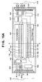
- Fig. 3 is a view schematically showing a semiconductor element substrate of this type for an inkjet printhead.
- heaters and driving circuits are integrally built in an element substrate 100 by a semiconductor process technology.
- Reference numeral 101 denotes a driver & heater array in which a plurality of heaters and a plurality of driver transistors serving as switching elements which are provided in correspondence with the heaters and switch whether to direct a current flow to the heaters are arrayed.
- Ink supply ports 102 supply ink from the lower surface of the element substrate.
- a shift register (S/R) 103 temporarily holds print data.
- a decoder 107 outputs a block enable signal to time-divisionally drive blocks of the heaters in the driver & heater array 101.
- Input circuits 104 include buffer circuits to input digital signals to the shift registers 103 and decoders 107.
- Input terminals 110 include a Vdd terminal to input a logic element voltage Vdd, a CLK terminal to input a clock (CLK) signal, and a DATA terminal to input print data (DATA).
- the digital circuits such as the shift registers and decoders are driven by a digital power supply voltage (voltage VDD).
- a level converter 116 converts a digital signal such as the VDD voltage driving signal into a VHT voltage signal to be given to the gate of each driver transistor.
- the voltage VHT is higher than the voltage VDD.
- a VHT voltage generation circuit 130 generates the voltage VHT to be supplied to the level converter 116 by stepping down a heater driving power supply voltage (VH).
- An AND circuit 119 serves as a heater selection circuit which calculates the logical product of a block enable signal and a print data signal.
- the AND circuit 119 includes, e.g., a buffer as needed.
- Fig. 5 is a timing chart for explaining a series of operations of sending a print data signal to the shift register 103 and supplying a current to the heaters to drive them.
- Print data is input to the DATA_A and DATA_B terminals in synchronism with the pulse of a clock signal input to the CLK terminal.
- the shift register 103 temporarily stores the input print data.
- a latch circuit holds the print data in accordance with a latch signal input to an LT terminal.
- the logical product of a block enable signal to select a heater group divided into desired blocks and the signal of print data (print data signal) held according to the latch signal is calculated.
- the signal of the calculated logical product synchronizes with an HE signal that directly determines the current driving time so that a current flows to desired heaters.
- the series of operations is repeated for the respective blocks, thereby executing printing.
- Fig. 4A is an equivalent circuit diagram corresponding to one segment having one heater and a corresponding driver in a conventional printing element.
- Fig. 4B is an equivalent circuit diagram corresponding to one bit of the shift register and latch circuit to temporarily store print data.
- the block enable signal input to an AND circuit 201 is supplied from the decoder 107.
- the block enable signal selects each heater group corresponding to one of divided blocks.
- the print data signal input to the AND circuit 201 is a signal input to the shift register 103 and held according to the latch signal.
- the AND circuit 201 serving as a heater selection circuit calculates the logical product of the block enable signal and print data signal.
- Reference numeral 205 denotes a VH power supply line; 206, a heater; and 207, a driver transistor serving as a switching element to direct a current flow to the heater 206.
- An inverter circuit 202 receives and buffers the output from the AND circuit 201.
- a VDD power supply line 203 serves as a power supply of the inverter circuit 202.
- a VHT power supply line 204 serves as a power supply to apply a voltage to the gate of the driver transistor 207.
- An inverter circuit 208 receives the voltage from the VHT power supply line.
- the inverter circuit 208 serves as a buffer to receive the buffer output from the inverter circuit 202.
- the inverter circuit 202, shift register 103, and the like are digital circuits in general and operate in accordance with a low or high pulse.
- a heat enable signal (HE) to designate a heater driving period is also a digital signal. Signal exchange with an external device is done by a low or high logic pulse.
- the voltage amplitudes of the digital signals are generally 0 V/5 V or 0 V/3.3 V.
- the power supply voltage of the digital circuits is VDD only.
- the above-described block enable signal and print data signal are input to the AND circuit 201 as the pulse of the voltage VDD and then input to the inverter circuit 208 of the next stage through the buffer formed from the two inverter circuits 202.
- the resistance value in the ON state i.e., so-called ON resistance of the driver transistor 207 is preferably as low as possible. In this case, since the power consumed by circuits except the heaters is minimized, an increase in the substrate temperature can be prevented, and stable printhead driving is possible. If the ON resistance of the driver transistor 207 is high, a current flows to this portion to make the voltage drop large. This requires to apply a higher voltage to the heater, and the power is wasted.
- the circuit shown in Fig. 4A it is necessary to convert the voltage into a pulse voltage higher than the voltage VDD.
- the circuit shown in Fig. 4A has the power supply line 204 of the voltage VHT higher than the voltage VDD so that the buffer circuit including the inverter circuit 208 converts the block enable signal input by the pulse of the voltage VDD into a pulse of the voltage VHT. After conversion, the pulse of the voltage VHT is applied to the gate of the driver transistor 207. That is, signal exchange with an external device and signal processing in the internal digital circuits are done in accordance with the pulse of the voltage VDD (logic circuit driving voltage).
- an amplitude conversion circuit which converts the voltage into the pulse of the voltage VHT (switching element driving voltage) is added to each segment immediately before driving the gate of the driver transistor 207.
- VHT switching element driving voltage
- reference numerals 116 denote the level converters of the plurality of segments.
- a printhead has a plurality of segments arrayed at a high density.
- the segments are arranged at a density of, e.g., 600 dpi, the array-direction width per segment is limited to about 42.3 ⁇ m.
- the size in a direction perpendicular to the array direction of the segments needs to increase.
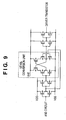
- Fig. 9 is an equivalent circuit diagram showing the detailed structure of the level converter portion in Fig. 4A .
- the level converter portion especially level conversion unit
- the area of the necessary element substrate increases.
- the length of the segment increases. This leads to an increase in the size of the element substrate for the printhead, resulting in an increase in cost. More specifically, in the above-described substrate structure, the element substrate spreads in the direction perpendicular to the segment array direction, and the size of the element substrate conspicuously increases.
- a level converter is added to each of, e.g., 256 segments of a printhead, at least 256 inverters are necessary, resulting in an increase in cost.
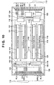
- U.S. Publication No. 2006/0209131 discloses a circuit arrangement which converts a logic circuit driving voltage into a printing element driving voltage without increasing the length in the direction perpendicular to the segment array direction.
- Fig. 10 is a view for explaining the arrangement of U.S. Publication No. 2006/0209131 .
- the same reference numerals as in Fig. 3 denote the same parts in Fig. 10 , and a description thereof will not be repeated unless they are particularly different from Fig. 3 .
- the level converter 116 is provided in the output stage of each decoder 107 and the output stage of each shift register 103.
- Fig. 2A is an equivalent circuit diagram, different from Fig. 4A , corresponding to one segment having one heater and a corresponding driver in a conventional printing element.
- Fig. 2B is an equivalent circuit diagram, different from Fig. 4B , corresponding to one bit of the shift register and latch circuit to temporarily store print data.
- the level converter is added to the output portion of each of the shift registers 103 and decoders 107, unlike the element substrate 100 in Figs. 3 and 4A in which the level converter is added to each segment. That is, the voltage rises before the AND circuit 201 calculates the logical product of the output signal (block enable signal) from the decoder 107 and the output signal (print data signal) from the shift register 103. Hence, as shown in Fig. 2A , a pulse signal stepped up to the voltage VHT is input to each segment. This obviates the level converter of each segment so that the area of the element substrate can be reduced.
- the transistors are formed from low-voltage-proof elements because only a low voltage corresponding to the logic circuit driving voltage is applied to this portion.
- the breakdown voltage of this portion is made higher than that for the transistors of the remaining logic circuits. More specifically, high-voltage-proof elements are used as the transistors included in the AND circuit.
- each transistor becomes larger than a low-voltage-proof transistor.
- the size of the element substrate 100 can be reduced because the number of level converters can be small, and they can be located far from the segments.
- Fig. 2B is a circuit diagram showing the arrangements of the shift register 103 and level converter 116.
- the level converter (amplitude conversion circuit) is added to the output stage of the shift register 103 shown in Fig. 4B to convert the pulse voltage from the voltage VDD to the voltage VHT.
- the number of output stages of the shift register 103 or decoder 107 is determined by the division count in time-divisionally driving all segments.
- the division count is about 8 to 32.
- the number greatly decreases as compared to the arrangement with the level converters 116 added to all segments. For this reason, the length of the element substrate 100 in the direction perpendicular to the segment array direction can decrease.
- the level converters 116 added to the shift registers 103 and decoders 107 increase the length of the element substrate 100 in the array direction. However, this increase is insignificant relative to the decrease in the length in the perpendicular direction.
- the total area of the element substrate 100 decreases.
- An inkjet printing apparatus is required to execute printing at a higher speed. For this reason, the number of orifices of the printhead increases, and the density of the orifices becomes high. Since the number of ink colors, the number of ink supply ports, and the number of orifice arrays also increase, the area of the element substrate becomes large.
- Fig. 12 is a view showing the arrangement and vertical positional relationship of two adjacent segments on an element substrate with a segment density of 1,200 dpi.
- heaters 206a for a medium discharge amount (2.5 pl) and heaters 206b for a small discharge amount (1 pl) are arranged at a pitch of 1,200 dpi from the side close to the ink supply port 102.
- Orifices are schematically illustrated on the heaters. These heaters are connected to transistors 207a and 207b by wirings (not shown).
- Corresponding level converters 116a and 116b are arranged on the side far from the ink supply port.
- the pitch is 1,200 dpi
- the array-direction width per segment is only 21 ⁇ m. For this reason, it is impossible to arrange two level converters in the segment array direction.
- Two level converters are arranged in the segment array direction and in the vertical direction. Since the area of a level converter is large, the width of the element substrate increases.
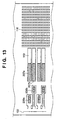
- Fig. 13 is a view showing the arrangement and vertical positional relationship of two adjacent segments.
- the heaters 206a for a medium discharge amount (2.5 pl) and the heaters 206b for a small discharge amount (1 pl) are arranged at a pitch of 1,200 dpi from the side close to the ink supply port 102. Orifices are schematically illustrated on the heaters. These heaters are connected to the transistors 207a and 207b by wirings (not shown).
- An AND circuit 119 which is operated by a high-voltage signal exists next to each transistor.
- Reference numeral 118 denotes wirings for a print data signal and block enable signal. The wirings 118 receive a high-voltage pulse signal, as described above.
- the high-voltage signal wirings are spaced apart from each other, and GND wirings are arranged between them, as indicated by dotted lines.
- the area occupied by the wirings 118 increases and cancels the width reducing effect obtained by eliminating level converters near the transistors.
- the present invention is directed to an element substrate, and a printhead, head cartridge, using the element substrate.
- the arrangement of the present invention it is possible to provide an inexpensive printhead element substrate which prevents an increase in the length in a direction perpendicular to the segment array direction even in a long-length high-definition head, and a printhead, head cartridge, and printing apparatus using the element substrate.
- a printhead element substrate as specified in any one of claims 1 to 5.
- a printhead as specified in claim 6.
- a head cartridge as specified in claim 7.
- the invention is particularly advantageous since it is possible to provide an inexpensive printhead element substrate which prevents an increase in the length in a direction perpendicular to the segment array direction even in a long-length high-definition head, and a printhead, head cartridge, using the element substrate.
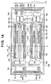
- Figs. 1A and 1B are views showing an inkjet printhead element substrate according to the first embodiment
- Figs. 2A and 2B are an equivalent circuit diagram corresponding to one segment of a driver and heater portion in a conventional printing element, and an equivalent circuit diagram corresponding to one bit of a shift register and a latch circuit, respectively;
- Fig. 3 is a view schematically showing an inkjet printhead element substrate
- Figs. 4A and 4B are an equivalent circuit diagram corresponding to one segment of a driver and heater portion in a conventional printing element, and an equivalent circuit diagram corresponding to one bit of a shift register and a latch circuit, respectively;
- Fig. 5 is a timing chart for explaining a series of operations of sending print information to the shift register and supplying a current to the heaters to drive them;
- Fig. 6 is an external perspective view showing the schematic arrangement of an inkjet printing apparatus according to a typical embodiment of the present invention.
- Fig. 7 is a block diagram showing the arrangement of a control circuit of the inkjet printing apparatus according to the typical embodiment of the present invention.
- Fig. 8 is an external perspective view showing the arrangement of a head cartridge that integrates an ink tank and a printhead according to a typical embodiment of the present invention
- Fig. 9 is an equivalent circuit diagram showing the detailed structure of a conventional level converter portion
- Fig. 10 is a view for explaining a conventional inkjet printhead element substrate
- Fig. 11 is a view showing the arrangement and vertical positional relationship of two adjacent segments in Fig. 1A ;
- Fig. 12 is a view showing the arrangement and vertical positional relationship of two adjacent segments in a conventional element substrate
- Fig. 13 is a view showing the arrangement and vertical positional relationship of two adjacent segments in a conventional element substrate
- Fig. 14 is a circuit diagram showing the circuits of two adjacent segments in Fig. 1A ;
- Figs. 15A and 15B are views showing an inkjet printhead element substrate according to the second embodiment.
- the terms "print” and “printing” not only include the formation of significant information such as characters and graphics, but also broadly includes the formation of images, figures, patterns, and the like on a print medium, or the processing of the medium, regardless of whether they are significant or insignificant and whether they are so visualized as to be visually perceivable by humans.
- the term "print medium” not only includes a paper sheet used in common printing apparatuses, but also broadly includes materials, such as cloth, a plastic film, a metal plate, glass, ceramics, wood, and leather, capable of accepting ink.
- ink includes a liquid which, when applied onto a print medium, can form images, figures, patterns, and the like, can process the print medium, and can process ink (e.g., can solidify or insolubilize a coloring agent contained in ink applied to the print medium).
- An "element substrate” in the description indicates not a simple substrate made of a silicon semiconductor but a substrate with elements and wirings.
- An expression “on an element substrate” indicates not only “on the surface of an element substrate” but also “inside of an element substrate near its surface”.
- a term “built-in” indicates not simply “arrange separate elements on a substrate” but “integrally form elements on an element substrate in a semiconductor circuit manufacturing process”.
- Fig. 6 is an external perspective view showing the schematic arrangement of an inkjet printing apparatus (IJRA) according to a typical embodiment of the present invention.
- IJRA inkjet printing apparatus
- a carriage HC engages with a helical groove 5004 of a lead screw 5005 which rotates via driving force transmission gears 5009 to 5011 interlockingly with the forward/reverse rotation of a driving motor 5013.
- the carriage HC has a pin (not shown) and reciprocally moves in the directions of arrows a and b while being supported by a guide rail 5003.
- An integrated inkjet cartridge IJC incorporating a printhead IJH and an ink tank IT is mounted on the carriage HC.
- a paper press plate 5002 presses a print medium P against a platen 5000 in the moving direction of the carriage HC.
- Photocouplers 5007 and 5008 confirm the presence of a lever 5006 of the carriage HC and detect whether the carriage HC is located at the home position to, e.g., switch the rotational direction of the motor 5013.
- a member 5016 supports a cap member 5022 that caps the front of the printhead IJH.
- a suction device 5015 sucks the cap to do suction recovery of the printhead through an opening 5023 in the cap.
- a cleaning blade 5017 and a member 5019 which moves the blade back and forth are supported by a main body support plate 5018. Not the blade with this form but any other known cleaning blade is applicable to the embodiment.
- a lever 5021 is used to start suction in suction recovery. The lever 5021 moves as a cam 5020 engaging with the carriage moves. The movement is controlled by a known transfer mechanism such as clutch switching to transfer the driving force from the driving motor.
- Fig. 7 is a block diagram showing the arrangement of the control circuit of the printing apparatus IJRA.
- reference numeral 1700 denotes an interface that inputs a print signal from, e.g., a host computer; 1701, an MPU; 1702, a ROM that stores a control program to be executed by the MPU 1701; 1703, a DRAM that saves various kinds of data (e.g., the print signal and print data to be supplied to the printhead IJH).
- a gate array (G.A.) 1704 controls print data supply to the printhead IJH and data transfer between the interface 1700, MPU 1701, and RAM 1703.
- a carrier motor 1710 conveys the printhead.
- a conveyance motor 1709 conveys a print medium.
- a motor driver 1706 drives the conveyance motor 1709.
- a motor driver 1707 drives the carrier motor 1710.
- Reference symbol IJH denotes a printhead.
- Reference numeral 100 denotes an element substrate.
- the control arrangement When a print signal is input to the interface 1700, the print signal is converted into print data for printing between the gate array 1704 and the MPU 1701. The motor drivers 1706 and 1707 are driven. In addition, the printhead IJH and element substrate 100 are driven in accordance with the print data so that printing is executed.
- Fig. 8 is an external perspective view showing the arrangement of the head cartridge IJC that integrates the ink tank and printhead.
- a dotted line K indicates the boundary between the ink tank IT and the printhead IJH.
- the head cartridge IJC has an electrode (not shown) to receive an electrical signal supplied from the side of a carriage C when the head cartridge IJC is mounted on the carriage C. The electrical signal drives the printhead IJH to discharge ink, as described above.
- Reference numeral 500 in Fig. 8 denotes an orifice array.
- element substrate driving method determination and circuit design are done in consideration of a fluid behavior for discharging ink droplets and making them fly in air and land.
- fundamental examinations to simultaneously achieve an appropriate element substrate area, high-speed printing, and high-definition image printing the present inventors examined the relationship between the element substrate driving method and the ink droplet landing accuracy by using a printhead having segments arranged at a density of 1,200 dpi.
- orifices for a discharge amount of 1 p1 are arranged on a side of the ink supply port at a pitch of 1,200 dpi while similar orifices are arranged on the other side by a shift corresponding to 2,400 dpi. That is, the orifices for a discharge amount of 1 pl are arranged on both sides at a pitch of 2,400 dpi.
- orifices for a small discharge amount e.g., 1 pl
- those for a medium discharge amount e.g., 2.5 pl
- the orifices for a medium discharge amount are used.
- the total number of times of discharge can decrease as compared to a case wherein only the orifices for a small discharge amount are used. It is therefore possible to execute high-speed printing by decreasing the number of passes.
- the orifices are arranged in consideration of the fluid behavior of ink droplets, and printing is done while thinning the orifices. Even a long-length printhead having orifices arranged at a high density can exhibit the element substrate area reduction effect at maximum while avoiding the problem posed by the circuit arrangement described in U.S. Publication No. 2006/0209131 .
- the present invention is not limited to this and is applicable to an arrangement which drives a plurality of adjacent heater at different timings.
- Figs. 1A and 1B are views showing an inkjet printhead element substrate according to this embodiment.
- a selection signal level converter 115 steps up a selection signal (SEL) (to be described later) to a switching transistor driving voltage (VHT).
- the selection signal level converter 115 is connected to selection circuits 117 each of which selects heaters to be driven by selecting switching elements to supply a driving signal.
- Fig. 1B is a sectional view taken along a line A - A in Fig. 1A .
- Ink supply ports 102 extend through the element substrate.
- orifices 141 are formed on the element substrate by using a photosensitive resin 140.
- Fig. 11 is a view showing the arrangement and vertical positional relationship of two adjacent segments in Fig. 1A .
- Fig. 14 is a circuit diagram showing the circuits of two segments adjacent in the direction of the length of the ink supply port 102 in Fig. 1A .
- heaters 206a for a medium discharge amount (2.5 pl) and heaters 206b for a small discharge amount (1 pl) are arranged at a pitch of 1,200 dpi from the side close to the ink supply port 102. Orifices are schematically illustrated on the heaters in Fig. 11 . These heaters are connected to transistors 207a and 207b serving as switching elements by wirings (not shown).
- the selection circuit 117 to select a driving target from the transistors 207a and 207b is provided between a level converter 116 and the transistors 207a and 207b.
- Reference numeral 118 denotes wirings for a block enable signal as a digital circuit power supply voltage signal and a print data signal.
- the wirings 118 are arranged in the direction of the length of the ink supply port 102, as shown in Fig. 1A .
- An AND circuit 119 serves as a heater selection circuit (electrothermal transducer selection circuit) which calculates the logical product of the block enable signal and the print data signal.
- the heater selection circuit need only selectively drive a heater on the basis of the block enable signal and print data signal, and any arrangement except the AND circuit may be used.
- the level converter 116 steps up the driving signal output from the AND circuit 119 to the switching transistor driving voltage (VHT).
- VHT switching transistor driving voltage
- the selection signal SEL to select the heaters 206b for achieving the small discharge amount or the heaters 206a for achieving the medium discharge amount is input from the outside of the element substrate and converted from the digital circuit power supply voltage level into a switching transistor driving voltage level by the selection signal level converter 115 near the connection pad spaced apart from the orifice array.
- the selection signal level converter 115 supplies the selection signal to the selection circuit 117 connected to the level converter 116 near the orifices through two wirings, i.e., the wirings of SEL and a logically inverted SELB.
- 1 (High) is input to the print data signal and block enable signal corresponding to the heaters 206a and 206b.
- the signals from the selection signal level converter 115 may commonly be input to selection circuits corresponding to a plurality of arrays.
- the selection circuit 117 shown in Fig. 14 includes NOR circuits.
- One input terminal 120 of the NOR circuit corresponding to the heater 206a and transistor 207a receives 0 (Low) when the print data signal and block enable signal are 1 (High).
- the NOR circuit outputs 1 only when all input terminals receive 0. In this case, the switching transistor 207a is driven to flow a current to the heater 206a.
- 0 is input to the selection signal SEL from the outside of the element substrate.
- the switching transistor 207b is driven to flow a current to the heater 206b.
- the switching transistor 207a is not driven.
- the switching transistors 207a and 207b are not driven simultaneously. Instead, they are driven exclusively. For this reason, the adjacent switching transistors 207a and 207b can share the level converter 116.
- the space between the wirings must be large, or GND wirings must be provided between the wirings.
- the wirings of the selection signals SEL and SELB are led to supply a high-voltage signal.
- Many wirings 118 of the block enable signal and print data signal supply a low-voltage signal (digital circuit power supply voltage) as usual. Since the minimum wiring rule is usable as usual, the element substrate area does not increase wastefully.
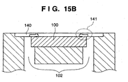
- Fig. 15A is a view showing an inkjet printhead element substrate according to the second embodiment.
- the first embodiment is applied to a printhead in which ink supply ports are provided in an element substrate to supply ink, and ink droplets are discharged in a direction perpendicular to the heater surface (on a side opposing the heater surface).
- the embodiment shown in Figs. 15A and 15B is applied to a printhead in which ink is supplied from the edges on both sides of an element substrate to discharge ink droplets in a direction perpendicular to the heater surface.
- Fig. 15B is a sectional view taken along a line A - A in Fig. 15A .
- Ink supply ports 102 extend on both sides of the element substrate.
- orifices 141 are formed on the element substrate by using a photosensitive resin 140.
- heaters for a small discharge amount and those for a medium discharge amount, which share level converters 116, are alternately arranged and exclusively driven, as in the first embodiment.
- orifices for different discharge amounts are exclusively driven.
- the arrangement of the present invention is also applicable to effectively reduce the area of the input terminal even in exclusively driving orifices for the same discharge amount.
Landscapes
- Particle Formation And Scattering Control In Inkjet Printers (AREA)
- Ink Jet (AREA)
Claims (7)
- Druckkopfelement-Substrat (100) mit:mehreren Elektrothermalwandlern (206);mehreren Schaltelementen (207), die entsprechend den mehreren Elektrothermalwandlern (206) vorgesehen sind, um letztere zu treiben;einer Elektrothermalwandler-Auswahlschaltung (119), dafür ausgelegt, ein Druckdatensignal und ein Blockfreigabesignal zu empfangen, um die mehreren Elektrothermalwandler (206) in mehrere Blöcke zu unterteilen sowie selektiv und auf Zeitmultiplexbasis die Blöcke zu treiben und ein Treibsignal auszugeben; undeinem Pegelkonverter (116), dafür ausgelegt, das Treibsignal aufwärts zu stufen;
dadurch gekennzeichnet, dassder Pegelkonverter (116) vorgesehen ist für eine Gruppe Schaltelemente (207a, 207b) entsprechend benachbarten Elektrothermalwandlern (206) unddas Druckkopfelement-Substrat (100) ferner umfasst:einen Auswahlsignal-Pegelkonverter (115), dafür ausgelegt, ein extern eingegebenes Auswahlsignal zum Auswählen eines zu treibenden Elektrothermalwandlers aufwärts zu stufen,eine Auswahlschaltung (117), dafür ausgelegt, sowohl das Auswahlsignal, das von dem Auswahlsignal-Pegelkonverter (115) aufwärts gestuft wird, und das von dem Pegelkonverter (116) aufwärts gestufte Treibsignal einzugeben als auch die Schaltelemente (207) auszuwählen, um die Elektrothermalwandler (206) zu treiben, und zwar auf der Basis des aufwärtsgestuften Auswahlsignals, das vom Auswahlsignal-Pegelkonverter (115) zugeführt wird, und des aufwärtsgestuften Treibsignals, das vom Pegelkonverter (116) zugeführt wird. - Substrat (100) nach Anspruch 1, ferner umfassend:eine Zeitmultiplex-Auswahlschaltung (107) zum Erzeugen des Blockfreigabesignals.
- Substrat (100) nach Anspruch 1, ferner umfassend:einen Tintenzufuhrdurchlass (102) zum Zuführen von Tinte, wobei
die mehreren Elektrothermalwandler (206) längs des Tintenzufuhrdurchlasses (102) angeordnet sind und
der Pegelkonverter (116) längs einer Anordnung der Elektrothermalwandler (206) angeordnet ist. - Substrat (100) nach Anspruch 2, wobei
Verdrahtungen (118) des Druckdatensignals und des Blockfreigabesignals angeordnet sind in einer Richtung längs einer Longitudinalrichtung des Tintenzufuhrdurchlasses (102). - Substrat (100) nach einem der Ansprüche 1 bis 4, wobei das Element-Substrat (100) für einen Tintenstrahldruckkopf (IJH) vorgesehen ist.
- Druckkopf (IJH), der versehen ist mit dem Element-Substrat (100) nach Anspruch 1.
- Kopfpatrone (IJC), die versehen ist mit dem Druckkopf (IJH) nach Anspruch 6.
Applications Claiming Priority (1)
| Application Number | Priority Date | Filing Date | Title |
|---|---|---|---|
| JP2006273414 | 2006-10-04 |
Publications (4)
| Publication Number | Publication Date |
|---|---|
| EP1908592A1 EP1908592A1 (de) | 2008-04-09 |
| EP1908592A8 EP1908592A8 (de) | 2008-07-02 |
| EP1908592B1 true EP1908592B1 (de) | 2010-09-01 |
| EP1908592B8 EP1908592B8 (de) | 2010-12-15 |
Family
ID=38724402
Family Applications (1)
| Application Number | Title | Priority Date | Filing Date |
|---|---|---|---|
| EP07018594A Not-in-force EP1908592B8 (de) | 2006-10-04 | 2007-09-21 | Komponententräger, Druckkopf und Kopfpatrone mit dem Komponententräger |
Country Status (7)
| Country | Link |
|---|---|
| US (2) | US7681992B2 (de) |
| EP (1) | EP1908592B8 (de) |
| JP (1) | JP5330572B2 (de) |
| KR (1) | KR100925066B1 (de) |
| CN (1) | CN101157298B (de) |
| DE (1) | DE602007008808D1 (de) |
| TW (1) | TWI403419B (de) |
Families Citing this family (13)
| Publication number | Priority date | Publication date | Assignee | Title |
|---|---|---|---|---|
| US9274807B2 (en) | 2006-04-20 | 2016-03-01 | Qualcomm Incorporated | Selective hibernation of activities in an electronic device |
| US8683362B2 (en) | 2008-05-23 | 2014-03-25 | Qualcomm Incorporated | Card metaphor for activities in a computing device |
| US8296684B2 (en) | 2008-05-23 | 2012-10-23 | Hewlett-Packard Development Company, L.P. | Navigating among activities in a computing device |
| EP1908592B8 (de) * | 2006-10-04 | 2010-12-15 | Canon Kabushiki Kaisha | Komponententräger, Druckkopf und Kopfpatrone mit dem Komponententräger |
| US8159469B2 (en) | 2008-05-06 | 2012-04-17 | Hewlett-Packard Development Company, L.P. | User interface for initiating activities in an electronic device |
| JP5723137B2 (ja) * | 2009-11-26 | 2015-05-27 | キヤノン株式会社 | 記録ヘッド用基板、記録ヘッド及び記録装置 |
| TWI516379B (zh) * | 2012-11-02 | 2016-01-11 | 國立交通大學 | 開關切換驅動方法 |
| JP6384251B2 (ja) | 2014-10-06 | 2018-09-05 | セイコーエプソン株式会社 | 液体噴射ヘッドおよび液体噴射装置 |
| JP6530601B2 (ja) * | 2014-12-16 | 2019-06-12 | キヤノン株式会社 | 液体吐出部品および液体吐出装置 |
| JP7005376B2 (ja) * | 2018-02-15 | 2022-01-21 | キヤノン株式会社 | 素子基板、記録ヘッド、及び記録装置 |
| JP7188068B2 (ja) * | 2018-03-02 | 2022-12-13 | 株式会社リコー | 液体吐出ヘッド、ヘッドモジュール、液体カートリッジ、液体吐出ユニットおよび液体吐出装置 |
| JP7191669B2 (ja) | 2018-12-17 | 2022-12-19 | キヤノン株式会社 | 液体吐出ヘッド用基板およびその製造方法 |
| JP7077461B1 (ja) * | 2021-06-03 | 2022-05-30 | キヤノン株式会社 | 記録素子基板および温度検知装置 |
Family Cites Families (14)
| Publication number | Priority date | Publication date | Assignee | Title |
|---|---|---|---|---|
| CA2075097C (en) | 1991-08-02 | 2000-03-28 | Hiroyuki Ishinaga | Recording apparatus, recording head and substrate therefor |
| KR100476950B1 (ko) * | 2002-12-06 | 2005-03-17 | 삼성전자주식회사 | 잉크젯 프린터의 헤드구동장치 및 그의 제어방법 |
| TWI246462B (en) * | 2003-06-10 | 2006-01-01 | Canon Kk | Ink-jet printhead substrate, driving control method, ink-jet printhead and ink-jet printing apparatus |
| US7125105B2 (en) * | 2003-09-08 | 2006-10-24 | Canon Kabushiki Kaisha | Semiconductor device for liquid ejection head, liquid ejection head, and liquid ejection apparatus |
| JP4353526B2 (ja) * | 2003-12-18 | 2009-10-28 | キヤノン株式会社 | 記録ヘッドの素子基体及び該素子基体を有する記録ヘッド |
| CN1628978A (zh) * | 2003-12-19 | 2005-06-22 | 明基电通股份有限公司 | 根据喷墨头温度调整喷墨能量的打印机与相关方法 |
| JP4137088B2 (ja) * | 2004-06-02 | 2008-08-20 | キヤノン株式会社 | ヘッド基板、記録ヘッド、ヘッドカートリッジ、記録装置、及び情報入出力方法 |
| US7559626B2 (en) * | 2004-12-09 | 2009-07-14 | Canon Kabushiki Kaisha | Inkjet recording head substrate and drive control method, inkjet recording head, inkjet recording head cartridge and inkjet recording apparatus |
| JP4785375B2 (ja) * | 2004-12-09 | 2011-10-05 | キヤノン株式会社 | インクジェット記録ヘッド用基板、記録ヘッド、ヘッドカートリッジ及び記録装置 |
| JP4678825B2 (ja) * | 2004-12-09 | 2011-04-27 | キヤノン株式会社 | ヘッド基板、記録ヘッド、ヘッドカートリッジ、及びその記録ヘッド或いはヘッドカートリッジを用いた記録装置 |
| JP2006168143A (ja) * | 2004-12-15 | 2006-06-29 | Canon Inc | インクジェット記録ヘッド |
| EP1908592B8 (de) * | 2006-10-04 | 2010-12-15 | Canon Kabushiki Kaisha | Komponententräger, Druckkopf und Kopfpatrone mit dem Komponententräger |
| US20080129782A1 (en) * | 2006-12-04 | 2008-06-05 | Canon Kabushiki Kaisha | Element substrate, printhead, head cartridge, and printing apparatus |
| JP2008149687A (ja) * | 2006-12-20 | 2008-07-03 | Canon Inc | インクジェット記録ヘッド用基板および該基板を用いるインクジェット記録ヘッド |
-
2007
- 2007-09-21 EP EP07018594A patent/EP1908592B8/de not_active Not-in-force
- 2007-09-21 DE DE602007008808T patent/DE602007008808D1/de active Active
- 2007-09-25 US US11/860,794 patent/US7681992B2/en not_active Expired - Fee Related
- 2007-09-29 CN CN2007101620177A patent/CN101157298B/zh not_active Expired - Fee Related
- 2007-10-02 KR KR1020070099450A patent/KR100925066B1/ko not_active Expired - Fee Related
- 2007-10-03 TW TW096137138A patent/TWI403419B/zh not_active IP Right Cessation
-
2010
- 2010-02-04 US US12/700,185 patent/US8191996B2/en not_active Expired - Fee Related
-
2012
- 2012-06-01 JP JP2012126502A patent/JP5330572B2/ja not_active Expired - Fee Related
Also Published As
| Publication number | Publication date |
|---|---|
| JP5330572B2 (ja) | 2013-10-30 |
| EP1908592B8 (de) | 2010-12-15 |
| KR100925066B1 (ko) | 2009-11-04 |
| CN101157298A (zh) | 2008-04-09 |
| TW200838706A (en) | 2008-10-01 |
| TWI403419B (zh) | 2013-08-01 |
| US8191996B2 (en) | 2012-06-05 |
| US7681992B2 (en) | 2010-03-23 |
| JP2012210814A (ja) | 2012-11-01 |
| EP1908592A1 (de) | 2008-04-09 |
| DE602007008808D1 (de) | 2010-10-14 |
| CN101157298B (zh) | 2010-07-07 |
| KR20080031645A (ko) | 2008-04-10 |
| US20080084440A1 (en) | 2008-04-10 |
| EP1908592A8 (de) | 2008-07-02 |
| US20100134566A1 (en) | 2010-06-03 |
Similar Documents
| Publication | Publication Date | Title |
|---|---|---|
| EP1908592B1 (de) | Komponententräger, Druckkopf und Kopfpatrone mit dem Komponententräger | |
| EP1543972B1 (de) | Elementplatte für Druckkopf und Druckkopf mit Elementplatte | |
| US8147039B2 (en) | Head substrate, printhead, head cartridge, and printing apparatus | |
| EP1312476B1 (de) | Aufzeichnungskopf und Aufzeichnungsgerät | |
| US6890048B2 (en) | Printhead and image printing apparatus | |
| US20080100649A1 (en) | Element substrate, and printhead, head cartridge, and printing apparatus using the element substrate | |
| US6382755B1 (en) | Printhead and printing apparatus using printhead | |
| EP1636036B1 (de) | Tintenstrahldruckkopfsubstrat, antriebssteuerverfahren, tintenstrahldruckkopf und tintenstrahldruckvorrichtung | |
| JP4537159B2 (ja) | 液体吐出ヘッド用半導体装置、液体吐出へッド及び液体吐出装置 | |
| EP2327549B1 (de) | Druckkopfsubstrat, Druckkopf und Druckvorrichtung | |
| US6331048B1 (en) | Inkjet printhead having multiple ink supply holes | |
| JP3997217B2 (ja) | インクジェット記録ヘッド用基板と駆動制御方法、インクジェット記録ヘッド及びインクジェット記録装置 | |
| JP4208431B2 (ja) | 記録ヘッド及び該記録ヘッドを用いた記録装置 | |
| US20240308209A1 (en) | Liquid discharge head substrate, liquid discharge head, and liquid discharge apparatus | |
| JP2004066601A (ja) | 記録ヘッドとその記録ヘッドを用いた記録装置 | |
| JP5014048B2 (ja) | 素子基板及び該素子基板を使用した記録ヘッド、ヘッドカートリッジ、記録装置 |
Legal Events
| Date | Code | Title | Description |
|---|---|---|---|
| PUAI | Public reference made under article 153(3) epc to a published international application that has entered the european phase |
Free format text: ORIGINAL CODE: 0009012 |
|
| AK | Designated contracting states |
Kind code of ref document: A1 Designated state(s): AT BE BG CH CY CZ DE DK EE ES FI FR GB GR HU IE IS IT LI LT LU LV MC MT NL PL PT RO SE SI SK TR |
|
| AX | Request for extension of the european patent |
Extension state: AL BA HR MK RS |
|
| RTI1 | Title (correction) |
Free format text: ELEMENT SUBSTRATE, AND PRINTHEAD, HEAD CARTRIDGE, AND PRINTING APPARATUS USING THE ELEMENT SUBSTRATE |
|
| 17P | Request for examination filed |
Effective date: 20081009 |
|
| AKX | Designation fees paid |
Designated state(s): DE FR GB IT |
|
| RTI1 | Title (correction) |
Free format text: ELEMENT SUBSTRATE, PRINTHEAD AND HEAD CARTRIDGE, USING THE ELEMENT SUBSTRATE |
|
| GRAP | Despatch of communication of intention to grant a patent |
Free format text: ORIGINAL CODE: EPIDOSNIGR1 |
|
| GRAS | Grant fee paid |
Free format text: ORIGINAL CODE: EPIDOSNIGR3 |
|
| GRAA | (expected) grant |
Free format text: ORIGINAL CODE: 0009210 |
|
| AK | Designated contracting states |
Kind code of ref document: B1 Designated state(s): DE FR GB IT |
|
| REG | Reference to a national code |
Ref country code: GB Ref legal event code: FG4D |
|
| REF | Corresponds to: |
Ref document number: 602007008808 Country of ref document: DE Date of ref document: 20101014 Kind code of ref document: P |
|
| PG25 | Lapsed in a contracting state [announced via postgrant information from national office to epo] |
Ref country code: IT Free format text: LAPSE BECAUSE OF FAILURE TO SUBMIT A TRANSLATION OF THE DESCRIPTION OR TO PAY THE FEE WITHIN THE PRESCRIBED TIME-LIMIT Effective date: 20100901 |
|
| PLBE | No opposition filed within time limit |
Free format text: ORIGINAL CODE: 0009261 |
|
| STAA | Information on the status of an ep patent application or granted ep patent |
Free format text: STATUS: NO OPPOSITION FILED WITHIN TIME LIMIT |
|
| 26N | No opposition filed |
Effective date: 20110606 |
|
| REG | Reference to a national code |
Ref country code: DE Ref legal event code: R097 Ref document number: 602007008808 Country of ref document: DE Effective date: 20110606 |
|
| REG | Reference to a national code |
Ref country code: FR Ref legal event code: PLFP Year of fee payment: 10 |
|
| PGFP | Annual fee paid to national office [announced via postgrant information from national office to epo] |
Ref country code: FR Payment date: 20160926 Year of fee payment: 10 |
|
| REG | Reference to a national code |
Ref country code: FR Ref legal event code: ST Effective date: 20180531 |
|
| PG25 | Lapsed in a contracting state [announced via postgrant information from national office to epo] |
Ref country code: FR Free format text: LAPSE BECAUSE OF NON-PAYMENT OF DUE FEES Effective date: 20171002 |
|
| PGFP | Annual fee paid to national office [announced via postgrant information from national office to epo] |
Ref country code: GB Payment date: 20200925 Year of fee payment: 14 |
|
| PGFP | Annual fee paid to national office [announced via postgrant information from national office to epo] |
Ref country code: DE Payment date: 20201127 Year of fee payment: 14 |
|
| REG | Reference to a national code |
Ref country code: DE Ref legal event code: R119 Ref document number: 602007008808 Country of ref document: DE |
|
| GBPC | Gb: european patent ceased through non-payment of renewal fee |
Effective date: 20210921 |
|
| PG25 | Lapsed in a contracting state [announced via postgrant information from national office to epo] |
Ref country code: GB Free format text: LAPSE BECAUSE OF NON-PAYMENT OF DUE FEES Effective date: 20210921 Ref country code: DE Free format text: LAPSE BECAUSE OF NON-PAYMENT OF DUE FEES Effective date: 20220401 |