EP1908205B1 - Testing method and apparatus for a transmission and reception system - Google Patents
Testing method and apparatus for a transmission and reception system Download PDFInfo
- Publication number
- EP1908205B1 EP1908205B1 EP06780059A EP06780059A EP1908205B1 EP 1908205 B1 EP1908205 B1 EP 1908205B1 EP 06780059 A EP06780059 A EP 06780059A EP 06780059 A EP06780059 A EP 06780059A EP 1908205 B1 EP1908205 B1 EP 1908205B1
- Authority
- EP
- European Patent Office
- Prior art keywords
- duty cycle
- signal
- receiver
- dcd
- clock
- Prior art date
- Legal status (The legal status is an assumption and is not a legal conclusion. Google has not performed a legal analysis and makes no representation as to the accuracy of the status listed.)
- Not-in-force
Links
- 238000012360 testing method Methods 0.000 title claims abstract description 66
- 230000005540 biological transmission Effects 0.000 title claims abstract description 13
- 230000000694 effects Effects 0.000 claims abstract description 9
- 238000010998 test method Methods 0.000 claims abstract description 4
- 238000000034 method Methods 0.000 claims description 45
- 238000005259 measurement Methods 0.000 claims description 24
- 238000011084 recovery Methods 0.000 claims description 17
- 230000000630 rising effect Effects 0.000 claims description 16
- 238000004458 analytical method Methods 0.000 claims description 14
- 230000003247 decreasing effect Effects 0.000 claims description 13
- 238000005070 sampling Methods 0.000 claims description 8
- 238000004590 computer program Methods 0.000 claims 3
- 238000001914 filtration Methods 0.000 claims 1
- 238000003780 insertion Methods 0.000 abstract description 8
- 230000037431 insertion Effects 0.000 abstract description 8
- 229920000729 poly(L-lysine) polymer Polymers 0.000 description 25
- 238000004519 manufacturing process Methods 0.000 description 13
- 230000007704 transition Effects 0.000 description 13
- 238000010586 diagram Methods 0.000 description 10
- 239000000872 buffer Substances 0.000 description 8
- 239000003990 capacitor Substances 0.000 description 7
- 238000004891 communication Methods 0.000 description 5
- 230000008569 process Effects 0.000 description 4
- 238000013459 approach Methods 0.000 description 3
- 238000013461 design Methods 0.000 description 3
- 230000004075 alteration Effects 0.000 description 2
- 230000001934 delay Effects 0.000 description 2
- 238000001514 detection method Methods 0.000 description 2
- 239000012464 large buffer Substances 0.000 description 2
- 238000012546 transfer Methods 0.000 description 2
- 244000287680 Garcinia dulcis Species 0.000 description 1
- 230000008901 benefit Effects 0.000 description 1
- 238000004422 calculation algorithm Methods 0.000 description 1
- 238000004364 calculation method Methods 0.000 description 1
- 238000003360 curve fit method Methods 0.000 description 1
- 230000007547 defect Effects 0.000 description 1
- 230000003111 delayed effect Effects 0.000 description 1
- 230000001419 dependent effect Effects 0.000 description 1
- 238000006073 displacement reaction Methods 0.000 description 1
- 238000009826 distribution Methods 0.000 description 1
- 230000006870 function Effects 0.000 description 1
- 235000021184 main course Nutrition 0.000 description 1
- 238000000691 measurement method Methods 0.000 description 1
- 238000012986 modification Methods 0.000 description 1
- 230000004048 modification Effects 0.000 description 1
- 230000010363 phase shift Effects 0.000 description 1
- 230000035945 sensitivity Effects 0.000 description 1
- 238000004088 simulation Methods 0.000 description 1
- 238000010972 statistical evaluation Methods 0.000 description 1
- 238000007619 statistical method Methods 0.000 description 1
- 230000001360 synchronised effect Effects 0.000 description 1
Images


Classifications
-
- H—ELECTRICITY
- H04—ELECTRIC COMMUNICATION TECHNIQUE
- H04L—TRANSMISSION OF DIGITAL INFORMATION, e.g. TELEGRAPHIC COMMUNICATION
- H04L1/00—Arrangements for detecting or preventing errors in the information received
- H04L1/20—Arrangements for detecting or preventing errors in the information received using signal quality detector
- H04L1/205—Arrangements for detecting or preventing errors in the information received using signal quality detector jitter monitoring
-
- G—PHYSICS
- G01—MEASURING; TESTING
- G01R—MEASURING ELECTRIC VARIABLES; MEASURING MAGNETIC VARIABLES
- G01R31/00—Arrangements for testing electric properties; Arrangements for locating electric faults; Arrangements for electrical testing characterised by what is being tested not provided for elsewhere
- G01R31/28—Testing of electronic circuits, e.g. by signal tracer
- G01R31/317—Testing of digital circuits
- G01R31/31725—Timing aspects, e.g. clock distribution, skew, propagation delay
-
- G—PHYSICS
- G01—MEASURING; TESTING
- G01R—MEASURING ELECTRIC VARIABLES; MEASURING MAGNETIC VARIABLES
- G01R31/00—Arrangements for testing electric properties; Arrangements for locating electric faults; Arrangements for electrical testing characterised by what is being tested not provided for elsewhere
- G01R31/28—Testing of electronic circuits, e.g. by signal tracer
- G01R31/317—Testing of digital circuits
- G01R31/3181—Functional testing
- G01R31/319—Tester hardware, i.e. output processing circuits
- G01R31/3193—Tester hardware, i.e. output processing circuits with comparison between actual response and known fault free response
- G01R31/31937—Timing aspects, e.g. measuring propagation delay
-
- H—ELECTRICITY
- H04—ELECTRIC COMMUNICATION TECHNIQUE
- H04L—TRANSMISSION OF DIGITAL INFORMATION, e.g. TELEGRAPHIC COMMUNICATION
- H04L1/00—Arrangements for detecting or preventing errors in the information received
- H04L1/24—Testing correct operation
- H04L1/242—Testing correct operation by comparing a transmitted test signal with a locally generated replica
Definitions
- This invention relates to the testing of a transmission and reception system, in particular to verify reliability of data transfer within equipment using the system.
- the transmission and reception system will typically be for providing data to, and receiving data from, a high-speed data bus which provides communication between different parts of an integrated circuit (IC) or between different ICs.
- IC integrated circuit
- Serial communication transceivers are widely used for data transfer between ICs, circuit boards and systems.
- the interfaces can operate at data rates above the capabilities of test equipment used in production, and this presents difficulties for the hardware testing.
- the high-speed interfaces need to correctly reconstruct received bits from the received signal in the presence of a certain level of distortion, particularly jitter.
- loop-back test A widely used alternative for specification-based testing in production is the use of a so-called "loop-back test", by which a known transmitter output is supplied to a receiver, and analysis of the received signal can be used to test the complete system characteristics.
- the loop-back test is typically supported by embedded pattern generation and bit error counters, in order to decrease test equipment requirements.
- a disadvantage of this method is that the range of defects that can be detected is limited for both the transmitter and receiver, particularly as the receiver is designed to tolerate certain amounts of jitter and attenuation from the transmitter.
- Phase locked loops are typically used for the generation of internal clock signals from an external system clock signal.
- the accuracy of different internal clock signals, with respect to the master system clock signal is one factor which influences the performance of the transmission and reception of data between different parts of the system which are operated by different internal clocks.
- Bit errors occur when interpreting received data if a recovered clock edge samples a neighbouring bit in the bit stream, and if this neighbouring bit has an opposite value. Due to jitter, the moment of the data transitions vary around their ideal moment. Jitter has different physical root-causes; some root-causes like thermal noise result in a Gaussian distributed probability (Random Jitter, RJ) while other root-causes like cross-talk cause deterministic jitter (DJ) and have other types of distributions. Since the RJ is unbounded there is always a probability of a bit error. In normal conditions, the design margin guarantees that the probability of a bit error is low, for example a probability (i.e. Bit Error Ratio) of 10 -12 is often used in specifications.
- a probability i.e. Bit Error Ratio
- Jitter can be inserted using a voltage-controlled variable delay element, generally driven by a sine wave.
- the jitter can be inserted on-chip or off-chip.
- the level of inserted jitter has to be known accurately to make this method suitable for production test.
- Off-chip implementation requires specific equipment as well as probing and routing of high-speed signals.
- On-chip jitter insertion often suffers from poor reliability under process, voltage and temperature variations.
- US 6,298,458 describes a system and method for manufacturing test of a physical layer transceiver.
- the system includes a built in self test (BIST) device that mimics distortion of an output wave form for testing an analog receiver under non-ideal conditions.
- BIST built in self test
- EP 0 889 411 describes a on-chip PLL phase and jitter self-test circuit.
- the circuit includes a series of delay elements that are used to generate delays in a system clock signal.
- Varying the duty cycle relationship provides duty cycle distortion (DCD), and this can be considered as a form of embedded jitter insertion.
- DCD duty cycle distortion
- This type of jitter can be measured relatively easily, for example with a low-pass filtered DC measurement.
- the DCD will be measured back the required accuracy of induced DCD is low, allowing the on-chip implementation of DCD to be relatively simple.
- the method does not require any alteration to the transmitter or receiver functional operation and can be implemented with low use of IC area and with simple test equipment.
- Varying a duty cycle relationship comprises varying the duty cycle of the test signal, for example in the path between the transmitter output and the receiver input.
- the analysis may comprise bit error ratio measurement.
- the combination of insertion of various amounts of DCD and bit-error ratio measurements allows a small number of measurements to be taken, in a sufficiently short time that is suitable for production testing.
- the measurement results can be used to calculate relevant jitter properties like random jitter (RJ), deterministic jitter (DJ) and total jitter (TJ).
- Total jitter is a known combination of the DJ and RJ characteristics of the transceiver under test, using statistical methods.
- the method of the invention can be used for (clock recovery) PLLs that lock on one edge, and can then measure jitter on rising and falling edges separately. This increases the diagnostic possibilities needed to find root-causes of detected faults.
- the method of the invention can also be used for PLLs that lock on both edges.
- DCD is added by splitting the high-speed signal in two branches.
- the high-speed signal is delayed by a programmable amount of time. This can be implemented by adding a programmable amount of load.
- the two branches can then be combined in parallel AND and OR gates.
- the AND gate output gives a decreased duty cycle while the OR gate gives an increased duty cycle.
- a multiplexer can then be used to select the decreased or increased duty cycle.
- the programmable load and multiplexer control can be provided by a shift register arrangement.
- the loop-backed high-speed signal with inserted DCD can be connected to receiver input pins.
- the actual amount of inserted DCD can be measured internally (on-chip), or off-chip on these Rx pins.
- PMU Parametric Measurement Unit
- DVM Digital Voltmeter
- the signal can be low-pass filtered by connecting resistors to the two differential Rx pins and a capacitor between the two resistor's other terminals. After a multiple of (e.g. 7) the RC time constant, a stable measurement of the DC voltage can be made, and for a ...010101... pattern, a 0V level is expected in the case of a 50% duty cycle. Under presence of DCD the resulting DC level will differ proportionally to the amount of DCD (which has units of time, such as picoseconds).
- the difference with the DC value when no DCD is inserted is of particular interest.
- This relative measurement can be made with good accuracy in a production test, limited for example by the PMU or DVM resolution, for example 250 micro-Volts for a typical test equipment PMU.
- the receiver typically uses a clock-and-data recovery (CDR) circuit having a PLL which locks to the received high-speed signal.
- CDR clock-and-data recovery
- PLL clock-and-data recovery
- locking can be done on one or both edges.
- the edge used by the PLL to lock can be made selectable, to enable detection of faults related to both edges.
- the inserted DCD will affect both edges.
- the recovered CDR clock is typically.used to sample the received high-speed data on both rising and falling edges. With the CDR locking on one edge of the high-speed signal, the DCD causes the opposite data edge to be displaced with respect to its normal position. This results in an increased probability of bit errors on those edges. Preferably, a bit-error counter in the receiver allows this probability to be measured.
- the measured inserted DCD and corresponding BER may be processed to determine a pass/fail condition.
- a statistical evaluation can be used to extract the relevant jitter levels from the measured DCD and corresponding BER.
- the invention is of particular benefit in detecting production faults in the transmitter or receiver hardware, which can cause increased jitter generation and/or decreased jitter tolerance, as these result in higher BER of the loop-backed signal.
- the invention relates to the testing of a transmission and reception system.
- the invention is of particular applicability to a system in which a Clock and Data Recovery (CDR) circuit is used in the receiver to derive clock timing information and perform data recovery from a received data stream.
- CDR Clock and Data Recovery
- Three main architectures can be classified as an over-sampling architecture, a tracking architecture and a phase-interpolation architecture.
- phase locked loop In a tracking architecture, a phase locked loop is used that locks on the received data.
- phase interpolation architecture which is essentially an alternative form of tracking
- the transmit clock is used and phase aligned with the incoming data, so only the phase is tracked. This is usually done by a loop that selects the phase that is closest to the data transition.
- the invention is based on the addition of duty-cycle distortion (DCD) to displace the position of data edges with respect to the recovered clock edges in a controlled and measurable way.
- DCD duty-cycle distortion
- the probability of bit errors, measured as a BER, will then be higher. From the measured edge displacement and corresponding BER the standard deviation of the RJ can be calculated, as well as the peak-to-peak level of the DJ.
- the introduced DCD When locking occurs on either the rising or falling edge of the received bitstream, the introduced DCD will essentially displace the opposite data edges with respect to the recovered clock edges, covering faults related to these edges. To cover faults related to the other edges, a test procedure is required that allows to select the edge on which the CDR PLL locks.
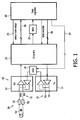
- Figure 1 shows a system of the invention for providing testability to a transmission and reception system, using DCD insertion.
- the apparatus comprises a transceiver 10 having a receiver 12 and a transmitter 14, and these interface between a high speed communications bus 15 and a serial circuit 16.
- a loopback path is defined between the output of the transmitter 14 and the input of the receiver, and this path includes a duty cycle distortion (DCD) element 18.
- the DCD element 18 is controlled by a test register 20 which also performs analysis of the signals received by the circuit 16 using the receiver 12. In the example shown, this analysis involved bit error ratio (BER) measurement, implemented by BER unit 22.
- BER bit error ratio
- Figure 1 also shows that the signal to which DCD has been applied is also supplied to a measurement circuit 26, which may be on or off-chip, and this enables measurement of the applied DCD before the signal has passed through the receiver.
- Figure 1 also shows that the test register 20 has a control output 25 "select lock edge". As will be described below, this may or may not be required, depending on the manner in which clock recovery is carried out.
- Figure 1 also shows data communications paths 26 between the test register and the circuitry 16.
- Figure 1 also shows a "test_enable" control signal which enables selection of different test modes, for example the loopback mode, a pattern generation mode, and an error compare mode.
- the implementation of the invention can be considered as five operations:
- the jitter analysis is not shown in Figure 1 , and this analysis can be implemented as software on the test equipment.
- the first three operation are the focus of this invention.
- Duty Cycle Distortion can be implemented in several different ways.
- One possibility is to use the intrinsic difference in fall and rise time of circuit elements.
- a standard multiplexer with two inputs A and B in a given CMOS process has a difference between fall and rise time of the order of 20ps.
- a chain of multiplexers can be configured, where each multiplexer output connects to input A of the next multiplexer, and input B connects to the original signal.
- Each multiplexer adds then a DCD of 20 ps to the signal; and the total DCD can be programmed by selecting the number of multiplexers in the signal path.
- This implementation of DCD has the disadvantage that the original signal is used to drive all multiplexer inputs B, which requires a large buffer for this signal.
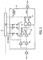
- Figure 2 shows an n+1 bit programmable DCD circuit
- the high-speed signal from the transmitter is used in two branches, "TXdelayed” (branch 30) and “TXbuf”. (branch 32).
- Each branch comprises first and second buffers 30a,30b and 32a,32b.
- the signal propagates with a certain delay through these branches.
- the delay can be increased by selectively adding load to the first buffer 30a.
- the drive strength of the buffer can be made programmable, if needed in combination with programmable load.
- Load-selection bits "DCD delay[0..n]” are programmed by shifting control bits into a test register 20 .
- the values of the loads are then chosen as a binary coded (1,2,4 .. 2 n ) multiple of a capacitance value x1.
- a linear array of switches S0 - Sn couple the capacitors to the output of the buffer 30a, where n+1 is the number of switches used.
- the control bits "DCD delay[0..n]” control the switches S0 to Sn, and when a switch is closed the capacitance is added to the load seen by the buffer.
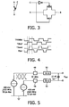
- Each switch S0 - Sn can be implemented as a transmission gate as shown in Figure 3 .
- the two branches TXdelayed and TXbuf in Figure 2 are used as inputs to an AND gate 40 as well as an OR gate 42 in parallel.
- the output of the AND gate “TXand” provides a signal with reduced duty cycle; and the OR gate output “TXor” provides a signal with increased duty-cycle.
- Figure 4 shows the signals in the two branches, and illustrates the outputs from the AND and OR gates for a given relative delay between the two branches. The difference in duty cycle between the signals TXand and TXor can clearly be seen.
- the increased or decreased duty-cycle signal is selected by a multiplexer 44 (shown in Figure 2 ).
- the multiplexer control signal "DC_decreate_increase" is provided by the test register 20.
- the buffers 30a,30b,32a,30b, AND/OR gates 40,42 and multiplexer 44 potentially add to the DCD, so that the DCD is not dependent solely on the capacitive load added. This is not critical since the DCD is also measured at the receiver pins by the circuitry 26 shown in Figure 1 .
- any DCD added by these circuits will be present as a DCD offset.
- An unbalanced offset could create the risk that the duty cycle cannot be increased or decreased sufficiently to produce a significant amount of bit errors in limited time.
- buffers are added in both branches 30,32, as shown, to make the default delay through both branches approximately equal.
- At least one buffer in the TXbuf branch 32 is needed to physically separate the two branches.
- the nominal delay in both branches should be equal.
- the duty-cycle distortion can be measured at the circuitry 26 (of Figure 1 ) in various ways, for example using an oscilloscope.
- An oscilloscope For production test it is preferred to have low requirements to equipment.
- One piece of equipment that is generally available in a test system is a Parametric Measurement Unit (PMU).
- PMU Parametric Measurement Unit
- a PMU can be used to measure DC voltage and currents.
- DVM Digital Voltmeter
- DVM Digital Voltmeter
- the PMU or DVM can also be used to measure the duty cycle of a bit-stream.
- a low-pass filter on the tester-to-device interface board, for example two resistors 50 connecting to the receiver pins 48 and a capacitor 52 connected to the other two terminals of the resistors, as shown schematically in Figure 1 and in more detail in Figure 5 .
- the resistor-capacitor arrangement functions as a low pass filter, and of course other filter configurations can be used.
- the DC value of the output voltage Vout measured between the two terminals of the capacitor is an RC charge curve, as represented in Figure 6 .
- circuit in figure 5 is of course only one example, and in other interface implementations voltage levels may be different, for example due to external DC biasing or an external load to a reference voltage.
- Figure 6 shows a simulation of low-pass filtered clock signals with 50% duty cycle (plot 60) and 49.5% duty cycle (plot 62).
- the reduced duty cycle corresponds to DCD of 2 ps.
- the resulting DC value is an average of the time 'high' minus the time 'low' of the high-speed signal.
- the 50% duty-cycle clock signal will approach a DC level of 0V at Vout.
- Vout DC , negative leg V max - 1 - e - t / RC * duty_cycle * V max - V min
- Vout DC Vout DC
- the output voltage can also be measured between one of the two capacitor terminals and a reference voltage (e.g. ground).
- a reference voltage e.g. ground
- the low-pass filter can be implemented on-chip, with on-chip switches connecting the low-pass filter to the high-speed signal.
- the output signal Vout has to be made observable at IC pins, for example using an analog test bus (for example IEEE 1149.4).
- the DC voltage measurement is directly affected by voltage amplitude as well as the duty-cycle.
- the output voltage levels are measured in a separate dedicated test, and these measured levels are used to determine the duty cycle in combination with the low-pass filtered DC test.
- Figure 7 shows a situation with a recovered clock at the full data rate.
- full rate and half rate CDRs are used.
- 1 clock cycle corresponds to 1 bit, and the rising edge is used for clock recovery, and the falling edge is used for data recovery.
- half rate CDR 1 clock cycle corresponds to 2 bits, and both the rising and falling edges are used for clock recovery.
- a 90 degree phase shifted clock is used for data recovery, and recovered clock has half the frequency of the data rate.
- Full data rate clock recovery is shown by way of example.
- the example signals in Figure 7 are for a "10101" pattern; for other patterns the displaced edge positions will differ according the transitions.
- the top plot 70 shows a 50% duty cycle.
- the next two plots 72, 74 show the transitions between 1 and 0 shifted to provide decreased and increased duty cycle respectively. The transitions move symmetrically about the center of the eye diagram. When the duty cycle is either decreased or increased, the probability of having an error in sampling any other bit increases.
- the plot 76 shows the recovered clock, in which the clock 1 to 0 transition has been timed with the center of the detected input data eye. This 1 to 0 clock transition is used to recover the data as represented by arrow 79.
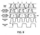
- Figure 8 again shows a recovered clock at the full data rate, and the different plots in Figure 8 correspond to those in Figure 7 .
- the example signals in Figure 8 are again for a "10101" pattern, and the displaced edges 80 are those associated with the falling edges of the data.
- the edge on which the PLL locks can be made to be switchable.
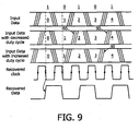
- Figure 9 shows the same plots as Figure 8 , but with the CDR signals locking on falling edges, so that the displaced edges 90 are those associated with the rising edges of the data.
- Figure 10 shows one way to implement a selectable lock edge, in which the data on which the PLL locks is inverted.
- An inverter is used to provide inverted data, and the original data and the inverted data are provided to a multiplexer 102 which selects one of the data signals based on a control input "Select_lock_edge".
- the control signal "select_lock_edge” can be provided by the test register 20.
- an XOR gate 110 can be used with the "Select_lock_edge" control signal and the data (“data_in”) as inputs.
- the differential polarity can simply be reversed to achieve inversion.
- Jitter is one of the main courses of bit errors in a serial transceiver.
- a high speed signal with increased DCD will be more susceptible to jitter and cause more bit errors.
- One way to use the programmable DCD is to increase DCD until a first bit error is observed. Since jitter is partly of a stochastic nature it is unpredictable when a bit error will occur. Therefore, it is preferred to count the number of bit errors, expressed as a bit-error ratio representing the number of received erroneous bits as ratio of the total number of received bits.
- Bit error counters are well known the art, and conventional devices can be used to implement the unit 22 shown in Figure 1 .
- the test equipment To perform the jitter analysis based on the obtained bit error ratio measurements, the test equipment records one or more DCD levels with the corresponding bit error ratios.
- a widely used method to analyse the performance of a receiver is to plot the BER versus eye-opening.
- the log-linear plot of BER versus eye-opening typically resembles the shape of a bathtub and is often referred to a bathtub curve.
- the level of random and deterministic jitter can be estimated using curve-fit techniques. For this, one or more measurement results with level of inserted DCD level and corresponding BER are needed. These jitter calculations also take into account how the clock recovery has been implemented, particularly whether the PLL lock is done on one or both edges.
- An example is a relative simple method using two bathtub curve points is an estimate curve fit method described in IEEE Std 802.3ae-2002, Section 48B.3.1.3.1 "Approximate curve fitting for BERT scan", pp 510-511 .
- This method estimates the random jitter ⁇ , deterministic jitter, peak-to-peak level and total jitter peak-to-peak level.
- Nr_observations is a pre-determined number of DCD-BER points used in the jitter analysis:
- the method implements a test mode in which a number N of BER measurements are taken for incrementally increasing DCD delay values.
- the N measurements correspond to the value "nr_observations”.
- This is performed by the sub-routine shown as 120. This sub-routine is performed for each lock edge and for increasing duty cycles and for decreasing duty cycles. Thus, four separate sets of data are obtained, and the sub-routine is called four times as shown.
- test sequence in that case is:
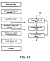
- This method is shown in Figure 13 .
- the method implements a test mode in which a number N of BER measurements are again taken for incrementally increasing DCD delay values. This is performed by the sub-routine shown as 130. and it is performed for increasing duty cycles and for decreasing duty cycles. Thus, two separate sets of data are obtained, and the sub-routine is called twice as shown.
- the invention can be applied for production testing of high speed interfaces.
- Examples of serial interfaces are Serial ATA, PCl Express, DVI, HDMI and USB 2.0.
- the invention can also be used for parallel types of interfaces such as Double Data Rate memory interfaces.
- the examples described above relate to serial communications systems in which a receiver recovers a clock and data from a serial bitstream.
- the invention can also be applied to applications of the invention in which a receiver has an externally provided clock. Also, it is possible to apply the DCD to the transmit clock instead of the data. This has the disadvantage of altering the functional circuit.
- Other applications may be to make a measurable delay between two sample times, where both sample times respond to different transitions of a clock for which duty cycle is altered and measured. Such a measurable delay might be applied for example in delay-fault testing of digital circuits.
- duty cycle distortion There may thus be considered to be two types of duty cycle distortion, and these may be considered as data DCD and clock DCD.
- data DCD With data DCD, with DCD inserted after the transmitter, a data "1" is made wider (for example) than a data "0". As a result, the common mode voltage increases, and the cross points in the eye diagram are not centered, but are shifted towards the high or lower rails, as shown in Figure 14a .
- the common mode voltage is half way between the voltage rails, and the eye diagram transitions shift in time, as shown in Figure 14b .
- the CDR can latch onto rising or falling edges or both.
- DCD DCD to provide a measurable affect on the probability of bit errors
- loopback test in order to increase the sensitivity of the loopback test.
- the DCD is inserted in a path between the transmitter and receiver.
- the transmitter and receiver pads are separated and a dedicated loopback path is inserted for test purposes.
- the transmitter and receiver pads can be shared, in which case the transmitter output and receiver input are the same. In these cases, there is no loopback path provided for test purposes.
- the invention can still however be implemented, by adding DCD in the functional path. This requires a bypass possibility for the functional signal, which can be implemented by alteration of the transmitter or receiver functional operation.
- DCD is measured using a filter and DC measurement technique.
- DCD can also be measured with other methods, on-chip and/or off-chip. For example, random sampling of the signal can be used, dividing the counted number of '1's by the total number of sampled bits.
Landscapes
- Engineering & Computer Science (AREA)
- Computer Networks & Wireless Communication (AREA)
- Signal Processing (AREA)
- General Engineering & Computer Science (AREA)
- Physics & Mathematics (AREA)
- General Physics & Mathematics (AREA)
- Quality & Reliability (AREA)
- Dc Digital Transmission (AREA)
- Synchronisation In Digital Transmission Systems (AREA)
- Test And Diagnosis Of Digital Computers (AREA)
Abstract
Description
- This invention relates to the testing of a transmission and reception system, in particular to verify reliability of data transfer within equipment using the system. For example, the transmission and reception system will typically be for providing data to, and receiving data from, a high-speed data bus which provides communication between different parts of an integrated circuit (IC) or between different ICs.
- Serial communication transceivers (transmitter/receiver devices) are widely used for data transfer between ICs, circuit boards and systems. The interfaces can operate at data rates above the capabilities of test equipment used in production, and this presents difficulties for the hardware testing. The high-speed interfaces need to correctly reconstruct received bits from the received signal in the presence of a certain level of distortion, particularly jitter.
- Considerable design effort is required to achieve the high data rates and guarantee operation under relevant process, voltage and temperature variations. As a consequence, small production flaws can cause the interface to be out of its specification limits.
- Existing production test methods aimed at detecting structural faults may not be capable of detecting all relevant production faults in the circuitry for high speed interfaces. It is possible to design test equipment specifically for a particular system to measure the jitter generation at the transmitter and jitter tolerance at the receiver. However, this is an expensive and time consuming approach and may not be viable.
- A widely used alternative for specification-based testing in production is the use of a so-called "loop-back test", by which a known transmitter output is supplied to a receiver, and analysis of the received signal can be used to test the complete system characteristics. The loop-back test is typically supported by embedded pattern generation and bit error counters, in order to decrease test equipment requirements.
- A disadvantage of this method is that the range of defects that can be detected is limited for both the transmitter and receiver, particularly as the receiver is designed to tolerate certain amounts of jitter and attenuation from the transmitter.
- Phase locked loops are typically used for the generation of internal clock signals from an external system clock signal. In synchronous systems, the accuracy of different internal clock signals, with respect to the master system clock signal, is one factor which influences the performance of the transmission and reception of data between different parts of the system which are operated by different internal clocks. There will typically be a phase shift between the system clock signal and the master clock signal, and the way this phase difference varies over time (the time derivative of phase difference) is defined as the timing jitter.
- Bit errors occur when interpreting received data if a recovered clock edge samples a neighbouring bit in the bit stream, and if this neighbouring bit has an opposite value. Due to jitter, the moment of the data transitions vary around their ideal moment. Jitter has different physical root-causes; some root-causes like thermal noise result in a Gaussian distributed probability (Random Jitter, RJ) while other root-causes like cross-talk cause deterministic jitter (DJ) and have other types of distributions. Since the RJ is unbounded there is always a probability of a bit error. In normal conditions, the design margin guarantees that the probability of a bit error is low, for example a probability (i.e. Bit Error Ratio) of 10-12 is often used in specifications.
- One known method to improve the detection capability of a loop-back test is to insert jitter into the high-speed signal. Jitter can be inserted using a voltage-controlled variable delay element, generally driven by a sine wave. The jitter can be inserted on-chip or off-chip. The level of inserted jitter has to be known accurately to make this method suitable for production test. Off-chip implementation requires specific equipment as well as probing and routing of high-speed signals. On-chip jitter insertion often suffers from poor reliability under process, voltage and temperature variations.
- An example of a self-test circuit for testing the PLL phase and jitter is described in
EP 0 889 411 -
US 6,298,458 describes a system and method for manufacturing test of a physical layer transceiver. The system includes a built in self test (BIST) device that mimics distortion of an output wave form for testing an analog receiver under non-ideal conditions. -
EP 0 889 411 - The invention is defined in the accompanying claims.
- Varying the duty cycle relationship provides duty cycle distortion (DCD), and this can be considered as a form of embedded jitter insertion. This type of jitter can be measured relatively easily, for example with a low-pass filtered DC measurement. Furthermore, since the DCD will be measured back the required accuracy of induced DCD is low, allowing the on-chip implementation of DCD to be relatively simple. In particular, the method does not require any alteration to the transmitter or receiver functional operation and can be implemented with low use of IC area and with simple test equipment.
- Varying a duty cycle relationship comprises varying the duty cycle of the test signal, for example in the path between the transmitter output and the receiver input.
- The analysis may comprise bit error ratio measurement. The combination of insertion of various amounts of DCD and bit-error ratio measurements allows a small number of measurements to be taken, in a sufficiently short time that is suitable for production testing. The measurement results can be used to calculate relevant jitter properties like random jitter (RJ), deterministic jitter (DJ) and total jitter (TJ). Total jitter is a known combination of the DJ and RJ characteristics of the transceiver under test, using statistical methods.
- The method of the invention can be used for (clock recovery) PLLs that lock on one edge, and can then measure jitter on rising and falling edges separately. This increases the diagnostic possibilities needed to find root-causes of detected faults. The method of the invention can also be used for PLLs that lock on both edges.
- In one implementation, DCD is added by splitting the high-speed signal in two branches. In one branch, the high-speed signal is delayed by a programmable amount of time. This can be implemented by adding a programmable amount of load. The two branches can then be combined in parallel AND and OR gates. The AND gate output gives a decreased duty cycle while the OR gate gives an increased duty cycle. A multiplexer can then be used to select the decreased or increased duty cycle.
- The programmable load and multiplexer control can be provided by a shift register arrangement.
- The loop-backed high-speed signal with inserted DCD can be connected to receiver input pins. The actual amount of inserted DCD can be measured internally (on-chip), or off-chip on these Rx pins. To measure this off-chip with the use of a signal tester Parametric Measurement Unit (PMU) or Digital Voltmeter (DVM) the signal can be low-pass filtered by connecting resistors to the two differential Rx pins and a capacitor between the two resistor's other terminals. After a multiple of (e.g. 7) the RC time constant, a stable measurement of the DC voltage can be made, and for a ...010101... pattern, a 0V level is expected in the case of a 50% duty cycle. Under presence of DCD the resulting DC level will differ proportionally to the amount of DCD (which has units of time, such as picoseconds).
- The difference with the DC value when no DCD is inserted is of particular interest. This relative measurement can be made with good accuracy in a production test, limited for example by the PMU or DVM resolution, for example 250 micro-Volts for a typical test equipment PMU.
- The receiver typically uses a clock-and-data recovery (CDR) circuit having a PLL which locks to the received high-speed signal. Depending on the PLL implementation, locking can be done on one or both edges. When the CDR PLL locking is performed using only one of the rising or falling edge, the edge used by the PLL to lock can be made selectable, to enable detection of faults related to both edges. When the PLL locks on both edges, the inserted DCD will affect both edges.
- The recovered CDR clock is typically.used to sample the received high-speed data on both rising and falling edges. With the CDR locking on one edge of the high-speed signal, the DCD causes the opposite data edge to be displaced with respect to its normal position. This results in an increased probability of bit errors on those edges. Preferably, a bit-error counter in the receiver allows this probability to be measured.
- Since the actual amount of inserted DCD may vary from chip to chip due to spread in process parameters, the measured inserted DCD and corresponding BER may be processed to determine a pass/fail condition. A statistical evaluation can be used to extract the relevant jitter levels from the measured DCD and corresponding BER.
- The invention is of particular benefit in detecting production faults in the transmitter or receiver hardware, which can cause increased jitter generation and/or decreased jitter tolerance, as these result in higher BER of the loop-backed signal.
- Examples of the invention will now be described in detail with reference to the accompanying drawings, in which :
-
Figure 1 shows a transmission and reception system of the invention; -
Figure 2 shows in more detail the duty cycle control unit use in the system ofFigure 1 ; -
Figure 3 shows how the switch in the unit ofFigure 2 can be implemented; -
Figure 4 shows a timing diagram for explaining the operation of the unit ofFigure 2 -
Figure 5 shows circuitry for measuring the duty cycle; -
Figure 6 shows is used to explain the operation of the circuit ofFigure 5 ; -
Figure 7 is a first example of timing diagram showing the effect of duty cycle variation; -
Figure 8 is a second example of timing diagram showing the effect of duty cycle variation; -
Figure 9 is a third example of timing diagram showing the effect of duty cycle variation; -
Figure 10 shows one way to switch between PLL lock edges; -
Figure 11 shows another way to switch between PLL lock edges; -
Figure 12 is a flow diagram for a first method of the invention; -
Figure 13 is a flow diagram for a second method of the invention; and -
Figures 14a and 14b show the effects of different types of duty cycle distortion on the eye diagram. - The invention relates to the testing of a transmission and reception system. The invention is of particular applicability to a system in which a Clock and Data Recovery (CDR) circuit is used in the receiver to derive clock timing information and perform data recovery from a received data stream.
- There are many different architectures suitable for CDR circuits. Three main architectures can be classified as an over-sampling architecture, a tracking architecture and a phase-interpolation architecture.
- In an over-sampling architecture, multiple samples are taken for each bit period. An algorithm decides which bit is best suited to use. For very high speed signals, it becomes impractical to build clocks that allow data over-sampling.
- In a tracking architecture, a phase locked loop is used that locks on the received data.
- With a phase interpolation architecture, which is essentially an alternative form of tracking, the transmit clock is used and phase aligned with the incoming data, so only the phase is tracked. This is usually done by a loop that selects the phase that is closest to the data transition.
- An example of the invention will now be given based on a tracking architecture, although it will be apparent that the invention can also be applied to other architectures.
- The invention is based on the addition of duty-cycle distortion (DCD) to displace the position of data edges with respect to the recovered clock edges in a controlled and measurable way. The probability of bit errors, measured as a BER, will then be higher. From the measured edge displacement and corresponding BER the standard deviation of the RJ can be calculated, as well as the peak-to-peak level of the DJ.
- When locking occurs on either the rising or falling edge of the received bitstream, the introduced DCD will essentially displace the opposite data edges with respect to the recovered clock edges, covering faults related to these edges. To cover faults related to the other edges, a test procedure is required that allows to select the edge on which the CDR PLL locks.
-
Figure 1 shows a system of the invention for providing testability to a transmission and reception system, using DCD insertion. - The apparatus comprises a
transceiver 10 having areceiver 12 and atransmitter 14, and these interface between a highspeed communications bus 15 and aserial circuit 16. A loopback path is defined between the output of thetransmitter 14 and the input of the receiver, and this path includes a duty cycle distortion (DCD)element 18. TheDCD element 18 is controlled by atest register 20 which also performs analysis of the signals received by thecircuit 16 using thereceiver 12. In the example shown, this analysis involved bit error ratio (BER) measurement, implemented byBER unit 22. The control of the DCD element is shown as 24.Figure 1 also shows that the signal to which DCD has been applied is also supplied to ameasurement circuit 26, which may be on or off-chip, and this enables measurement of the applied DCD before the signal has passed through the receiver. -
Figure 1 also shows that thetest register 20 has acontrol output 25 "select lock edge". As will be described below, this may or may not be required, depending on the manner in which clock recovery is carried out.Figure 1 also showsdata communications paths 26 between the test register and thecircuitry 16.Figure 1 also shows a "test_enable" control signal which enables selection of different test modes, for example the loopback mode, a pattern generation mode, and an error compare mode. The implementation of the invention can be considered as five operations: - DCD insertion;
- DCD measurement;
- Selection of lock edge (if required);
- BER measurement; and
- Jitter analysis
- The jitter analysis is not shown in
Figure 1 , and this analysis can be implemented as software on the test equipment. The first three operation are the focus of this invention. - The insertion of Duty Cycle Distortion can be implemented in several different ways. One possibility is to use the intrinsic difference in fall and rise time of circuit elements. For example, a standard multiplexer with two inputs A and B in a given CMOS process has a difference between fall and rise time of the order of 20ps. A chain of multiplexers can be configured, where each multiplexer output connects to input A of the next multiplexer, and input B connects to the original signal. Each multiplexer adds then a DCD of 20 ps to the signal; and the total DCD can be programmed by selecting the number of multiplexers in the signal path. This implementation of DCD has the disadvantage that the original signal is used to drive all multiplexer inputs B, which requires a large buffer for this signal.
- An example method of implementing duty cycle distortion will be described with reference to
Figure 2 , and which avoids the need for a large buffer.Figure 2 shows an n+1 bit programmable DCD circuit - In the
DCD insertion circuit 18 ofFigure 2 , the high-speed signal from the transmitter is used in two branches, "TXdelayed" (branch 30) and "TXbuf". (branch 32). Each branch comprises first andsecond buffers branch 30 "TXdelayed", the delay can be increased by selectively adding load to thefirst buffer 30a. As alternative, the drive strength of the buffer can be made programmable, if needed in combination with programmable load. - Load-selection bits "DCD delay[0..n]" are programmed by shifting control bits into a
test register 20 . The values of the loads are then chosen as a binary coded (1,2,4 .. 2n) multiple of a capacitance value x1. A linear array of switches S0 - Sn couple the capacitors to the output of thebuffer 30a, where n+1 is the number of switches used. The control bits "DCD delay[0..n]" control the switches S0 to Sn, and when a switch is closed the capacitance is added to the load seen by the buffer. - Each switch S0 - Sn can be implemented as a transmission gate as shown in
Figure 3 . - The two branches TXdelayed and TXbuf in
Figure 2 are used as inputs to an ANDgate 40 as well as anOR gate 42 in parallel. The output of the AND gate "TXand" provides a signal with reduced duty cycle; and the OR gate output "TXor" provides a signal with increased duty-cycle. -
Figure 4 shows the signals in the two branches, and illustrates the outputs from the AND and OR gates for a given relative delay between the two branches. The difference in duty cycle between the signals TXand and TXor can clearly be seen. - The increased or decreased duty-cycle signal is selected by a multiplexer 44 (shown in
Figure 2 ). The multiplexer control signal "DC_decreate_increase" is provided by thetest register 20. - The
buffers gates multiplexer 44 potentially add to the DCD, so that the DCD is not dependent solely on the capacitive load added. This is not critical since the DCD is also measured at the receiver pins by thecircuitry 26 shown inFigure 1 . - However, any DCD added by these circuits will be present as a DCD offset. An unbalanced offset could create the risk that the duty cycle cannot be increased or decreased sufficiently to produce a significant amount of bit errors in limited time.
- For this reason, buffers are added in both
branches TXbuf branch 32 is needed to physically separate the two branches. To allow the range of programmable DCD decrease and increase to be as equal as possible, the nominal delay in both branches should be equal.. - The duty-cycle distortion can be measured at the circuitry 26 (of
Figure 1 ) in various ways, for example using an oscilloscope. For production test it is preferred to have low requirements to equipment. One piece of equipment that is generally available in a test system is a Parametric Measurement Unit (PMU). A PMU can be used to measure DC voltage and currents. In testers equipped with a Digital Voltmeter (DVM) the DVM can also be used. - With the addition of a low-pass filter the PMU or DVM can also be used to measure the duty cycle of a bit-stream. One implementation is to add a low-pass filter on the tester-to-device interface board, for example two
resistors 50 connecting to the receiver pins 48 and acapacitor 52 connected to the other two terminals of the resistors, as shown schematically inFigure 1 and in more detail inFigure 5 . The resistor-capacitor arrangement functions as a low pass filter, and of course other filter configurations can be used. - The DC value of the output voltage Vout measured between the two terminals of the capacitor is an RC charge curve, as represented in
Figure 6 . The time constant is derived from the sum of the two resistors (i.e. 2*50=100 Ohm for the values used inFigure 5 ). - The circuit in
figure 5 is of course only one example, and in other interface implementations voltage levels may be different, for example due to external DC biasing or an external load to a reference voltage. -
Figure 6 shows a simulation of low-pass filtered clock signals with 50% duty cycle (plot 60) and 49.5% duty cycle (plot 62). The reduced duty cycle corresponds to DCD of 2 ps. The resulting DC value is an average of the time 'high' minus the time 'low' of the high-speed signal. The 50% duty-cycle clock signal will approach a DC level of 0V at Vout. In general, the DC output voltage on the positive leg will be: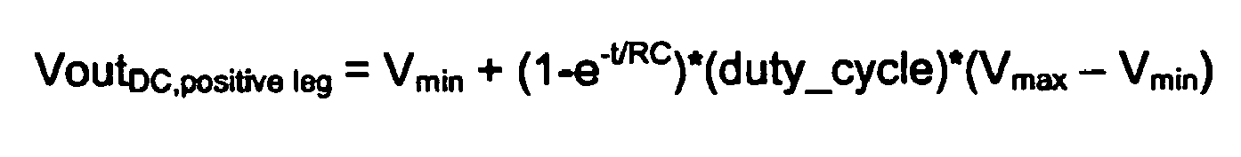
- With Vmax and Vmin being the 'high' respectively 'low' voltage. Similarly, the DC output on the negative leg is:

- The resulting DC output voltage Vout over the capacitor terminals is the difference:

- For the example of
Figure 6 , the signal with 49.5% duty cycle, for Vmax=400mV and Vmin=0V will approach:
- The output voltage can also be measured between one of the two capacitor terminals and a reference voltage (e.g. ground). This has the disadvantage that the resulting difference between voltages will be proportional to the duty-cycle-distortion times the voltage swing, rather than proportional to double this value (as in the equations above).
- The low-pass filter can be implemented on-chip, with on-chip switches connecting the low-pass filter to the high-speed signal. The output signal Vout has to be made observable at IC pins, for example using an analog test bus (for example IEEE 1149.4).
- The DC voltage measurement is directly affected by voltage amplitude as well as the duty-cycle. Typically, the output voltage levels are measured in a separate dedicated test, and these measured levels are used to determine the duty cycle in combination with the low-pass filtered DC test.
- As mentioned above, there is an option of selecting how to implement the lock edge for clock recovery. There are essentially two options, one is the use of a PLL which locks on both edges, and the other is the use of a PLL which locks on one edge.
- The use of PLLs that lock on both edges within the clock and data recovery (CDR) circuit results in both data edges being displaced with respect to their ideal location as a result of the introduction of DCD. Thus, both edges contribute to an increased BER.
-
Figure 7 shows a situation with a recovered clock at the full data rate. Of course, a different clock rate rata versus data rate is possible. Most commonly, full rate and half rate CDRs are used. For a full rate CDR, 1 clock cycle corresponds to 1 bit, and the rising edge is used for clock recovery, and the falling edge is used for data recovery. For a half rate CDR, 1 clock cycle corresponds to 2 bits, and both the rising and falling edges are used for clock recovery. A 90 degree phase shifted clock is used for data recovery, and recovered clock has half the frequency of the data rate. Full data rate clock recovery is shown by way of example. - The example signals in
Figure 7 are for a "10101" pattern; for other patterns the displaced edge positions will differ according the transitions. - The
top plot 70, of the input data, shows a 50% duty cycle. The next twoplots 72, 74 show the transitions between 1 and 0 shifted to provide decreased and increased duty cycle respectively. The transitions move symmetrically about the center of the eye diagram. When the duty cycle is either decreased or increased, the probability of having an error in sampling any other bit increases. - The
plot 76 shows the recovered clock, in which theclock 1 to 0 transition has been timed with the center of the detected input data eye. This 1 to 0 clock transition is used to recover the data as represented byarrow 79. - The use of PLLs that lock on one edge results in the data edge on which the CDR PLL will lock to be fixed. The data edges opposite to the edges on which the PLL locks are the displaced edges and faults related to these edges will contribute to the BER.
Figure 8 again shows a recovered clock at the full data rate, and the different plots inFigure 8 correspond to those inFigure 7 . - The example signals in
Figure 8 are again for a "10101" pattern, and the displacededges 80 are those associated with the falling edges of the data. - If the duty cycle is decreased, and locking occurs on rising edges (as in the second plot of
Figure 8 ), the probability increases of having an error in sampling the last high bit before a transition to low. - When the duty cycle is increased (the third plot in
Figure 8 ), the probability increases of having an error in sampling the next low bit just after a transition to low increases. - From the above, it can be seen that under presence of inserted DCD, the jitter related to the edge on which the PLL locks will not increase the BER, only jitter related to the next transition will increase the BER.
- Potential faults related to the data edges on which the PLL locks are then not detected.
- To overcome this possible drawback, the edge on which the PLL locks can be made to be switchable.
-
Figure 9 shows the same plots asFigure 8 , but with the CDR signals locking on falling edges, so that the displacededges 90 are those associated with the rising edges of the data. - In this case, if the duty cycle is decreased (second plot in
Figure 9 ), the probability of having errors related to the rising edges increase. Similarly, if the duty cycle is decreased, the probability of having errors related to the falling edges increases (third plot inFigure 9 ). - In this way, by making the locking edge selectable, all rising and falling transitions contributing to BER can separately be tested. This is the purpose of the
control signal 25 inFigure 1 . -
Figure 10 shows one way to implement a selectable lock edge, in which the data on which the PLL locks is inverted. - An inverter is used to provide inverted data, and the original data and the inverted data are provided to a
multiplexer 102 which selects one of the data signals based on a control input "Select_lock_edge". The control signal "select_lock_edge" can be provided by thetest register 20. - As a second example, shown in
Figure 11 , anXOR gate 110 can be used with the "Select_lock_edge" control signal and the data ("data_in") as inputs. - As a third alternative, if the signals used are differential signals, the differential polarity can simply be reversed to achieve inversion.
- As outlined above, the aim of the analysis to be carried out is to perform jitter measurement and tests. Jitter is one of the main courses of bit errors in a serial transceiver. A high speed signal with increased DCD will be more susceptible to jitter and cause more bit errors.
- One way to use the programmable DCD is to increase DCD until a first bit error is observed. Since jitter is partly of a stochastic nature it is unpredictable when a bit error will occur. Therefore, it is preferred to count the number of bit errors, expressed as a bit-error ratio representing the number of received erroneous bits as ratio of the total number of received bits.
- Bit error counters are well known the art, and conventional devices can be used to implement the
unit 22 shown inFigure 1 . - To perform the jitter analysis based on the obtained bit error ratio measurements, the test equipment records one or more DCD levels with the corresponding bit error ratios.
- A widely used method to analyse the performance of a receiver is to plot the BER versus eye-opening. The log-linear plot of BER versus eye-opening typically resembles the shape of a bathtub and is often referred to a bathtub curve.
- From the bathtub curve, the level of random and deterministic jitter can be estimated using curve-fit techniques. For this, one or more measurement results with level of inserted DCD level and corresponding BER are needed. These jitter calculations also take into account how the clock recovery has been implemented, particularly whether the PLL lock is done on one or both edges.
- An example is a relative simple method using two bathtub curve points is an estimate curve fit method described in IEEE Std 802.3ae-2002, Section 48B.3.1.3.1 "Approximate curve fitting for BERT scan", pp 510-511. This method estimates the random jitter σ, deterministic jitter, peak-to-peak level and total jitter peak-to-peak level. With this method the quantiles of two BER levels are plotted against the eye-opening. The slope of the straight line drawn between these points corresponds to the random jitter (RJ) level, the point where the quantile (BER)=0 line is crossed indicates the peak-to-peak level of deterministic jitter (DJ). The RJ and DJ are combined in TJ according to TJ=DJ+13.8*RJ.
- As an example of the usage of the invention for production testing, the following steps can be implemented to complete a jitter test; applied to a PLL that locks on one edge. "Nr_observations" is a pre-determined number of DCD-BER points used in the jitter analysis:
- (i) Select loop-back test mode
- (ii) Program DCD delay=0, DC_increase_decrease='0', select_lock_edge='0'
- (iii) Start transmitting patterns
- (iv) Measure and store DCD and BER
- (v) Increase DCD delay
- (vi) Repeat steps (iv)- (v) another "nr_observations-1" times
- (vii) Program DCD delay=0, DC_increase_decrease='0', select_lock_edge='1'
- (viii) Repeat steps (iv) - (vi)
- (ix) Program DCD delay=0, DC_increase_decrease='1', select_lock_edge='0'
- (x) Repeat steps (iv) - (vi)
- (xi) Program DCD delay=0, DC_increase_decrease='1', select_lock_edge='1',
- (xii) Repeat steps (iv) - (vi)
- (xiiii) Perform jitter analysis: calculate RJ, DJ and TJ
- (xiv) Decide pass or fail
- (xv) Stop transmitting patterns
- This method is shown in
Figure 12 . The method implements a test mode in which a number N of BER measurements are taken for incrementally increasing DCD delay values. The N measurements correspond to the value "nr_observations". This is performed by the sub-routine shown as 120. This sub-routine is performed for each lock edge and for increasing duty cycles and for decreasing duty cycles. Thus, four separate sets of data are obtained, and the sub-routine is called four times as shown. - In case of a PLL that locks on both edges the signal "select_lock_edge" is not used. The test sequence in that case is:
- (i) Select loop-back test mode
- (ii) Program DCD delay=0, DC_increase_decrease='0'
- (iii) Start transmitting patterns
- (iv) Measure and store DCD and BER
- (v) Increase DCD delay
- (vi) Repeat steps (iv) - (v) another "nr_observations-1" times
- (vii) Program DCD delay=0, DC_increase_decrease='1'
- (viii) Repeat steps (iv) - (vi)
- (ix) Perform jitter analysis: calculate RJ, DJ and TJ
- (x) Decide pass or fail
- (xi) Stop transmitting patterns
- This method is shown in
Figure 13 . The method implements a test mode in which a number N of BER measurements are again taken for incrementally increasing DCD delay values. This is performed by the sub-routine shown as 130. and it is performed for increasing duty cycles and for decreasing duty cycles. Thus, two separate sets of data are obtained, and the sub-routine is called twice as shown. - The invention can be applied for production testing of high speed interfaces. Examples of serial interfaces are Serial ATA, PCl Express, DVI, HDMI and USB 2.0. The invention can also be used for parallel types of interfaces such as Double Data Rate memory interfaces.
- The examples shown generally use single polarity signals. However, the use of differential signals in circuits of the invention is also possible.
- The examples described above relate to serial communications systems in which a receiver recovers a clock and data from a serial bitstream. The invention can also be applied to applications of the invention in which a receiver has an externally provided clock. Also, it is possible to apply the DCD to the transmit clock instead of the data. This has the disadvantage of altering the functional circuit. Other applications may be to make a measurable delay between two sample times, where both sample times respond to different transitions of a clock for which duty cycle is altered and measured. Such a measurable delay might be applied for example in delay-fault testing of digital circuits.
- There may thus be considered to be two types of duty cycle distortion, and these may be considered as data DCD and clock DCD. With data DCD, with DCD inserted after the transmitter, a data "1" is made wider (for example) than a data "0". As a result, the common mode voltage increases, and the cross points in the eye diagram are not centered, but are shifted towards the high or lower rails, as shown in
Figure 14a . - With clock DCD, with DCD inserted before the transmitter and applied to the transmit clock, the common mode voltage is half way between the voltage rails, and the eye diagram transitions shift in time, as shown in
Figure 14b . The CDR can latch onto rising or falling edges or both. - The use of DCD to provide a measurable affect on the probability of bit errors can be used in other examples of loopback test, in order to increase the sensitivity of the loopback test.
- In the example above, the DCD is inserted in a path between the transmitter and receiver. For some High Speed I/O interfaces (such as PCI Express), the transmitter and receiver pads are separated and a dedicated loopback path is inserted for test purposes. However, in other bi-directional interfaces (such as USB2.0) the transmitter and receiver pads can be shared, in which case the transmitter output and receiver input are the same. In these cases, there is no loopback path provided for test purposes. The invention can still however be implemented, by adding DCD in the functional path. This requires a bypass possibility for the functional signal, which can be implemented by alteration of the transmitter or receiver functional operation.
- In the example above, DCD is measured using a filter and DC measurement technique. DCD can also be measured with other methods, on-chip and/or off-chip. For example, random sampling of the signal can be used, dividing the counted number of '1's by the total number of sampled bits.
- Various other modifications will be apparent to those skilled in the art.
Claims (25)
- A method of testing a data transmission and reception system, the method comprising:sending a test signal from a transmitter (14) of the system to a receiver (12) of the system; andanalyzing the received signal,
wherein the method also comprises:varying a duty cycle relationship between the test signal and a timing signal used by the receiver of the system, wherein said varying the duty cycle relationship comprises varying a duty cycle of the test signal by splitting the test signal sent by the transmitter into two branches (30, 32), and delaying the signal of one branch by a programmable amount of time, and combining the signals of the two branches; andanalyzing the effect of the duty cycle variation. - A method as claimed in claim 1, wherein the duty cycle of the test signal is varied in the path between the transmitter output and the receiver input.
- A method as claimed in claim 1 or claim 2, wherein the signals in the two branches are combined using parallel AND (40) and OR (42) gates, and the method further comprises selecting an increased or decreased duty cycle using a multiplexer (44).
- A method as claimed in any preceding claim, wherein delaying the signal of one branch comprises adding a programmable amount of load.
- A method as claimed in any of claims 1 to 3, wherein delaying the signal of one branch comprises using a programmable drive strength.
- A method as claimed in any preceding claim, wherein the method further comprises low-pass filtering the signal provided to the receiver, and measuring a dc voltage which represents the duty cycle.
- A method as claimed in any preceding claim, wherein the method further comprises sampling the signal provided to the receiver, counting the number of sampled '1's and/or '0's, where the ratio of counted '1's to the total number of samples represents the duty cycle.
- A method as claimed in any preceding claim, wherein the analysis comprises bit error ratio measurement.
- A method as claimed in any preceding claim, wherein analyzing the received signal comprises providing a pass or fail indication based on the duty cycle variation and a measured receiver error rate
- A method as claimed in any preceding claim, wherein analyzing the received signal comprises calculating the jitter from the duty cycle variation and a measured receiver error rate.
- A method as claimed in any preceding claim, wherein the method further comprises performing clock recovery from received data in the receiver and using the recovered clock to interpret the received data.
- A method as claimed in claim 11, wherein the method comprises performing clock recovery from rising and falling edges of the received data.
- A method as claimed in claim 11, wherein the method comprises performing clock recovery from the rising or falling edges of the received data, and wherein the method further comprises analyzing the effect of duty cycle variation for a recovered clock using the rising edges of the received data and for a recovered clock using the falling edges of the received data.
- An apparatus for testing a data transmission and reception system, comprising:means (20) for generating a test signal for transmission;means (18) for varying a duty cycle relationship between the test signal and the timing signal used by the receiver (12) of the system, wherein said means for varying the duty cycle relationship comprises means for varying a duty cycle of the test signal by splitting the test signal sent by the transmitter into two branches (30, 32), and .delaying the signal of one branch by a programmable amount of time, and combining the signals of the two branches; andmeans (22) for analyzing a received signal which comprises the transmitted signal after the effect of duty cycle variation, thereby to analyze the effect of the duty cycle variation.
- An apparatus as claimed in claim 14, wherein the means for analyzing comprises a bit error ratio measurement circuit (22).
- An apparatus as claimed in claim 14 or 15, wherein the means for varying the duty cycle comprises:a splitter for splitting the transmitter output into two branches (30, 32),a delay element for delaying the signal of one branch (30) by said programmable amount of time; anda combiner (40, 42, 44) for combining the signals of the two branches.
- An apparatus as claimed in claim 16, wherein the combiner comprises parallel AND (40) and OR (42) gates, and a multiplexer (44) for selecting the output of one of the gates.
- An apparatus as claimed in claim 16 or 17, wherein the delay element comprises a variable load.
- An apparatus as claimed in any one of claims 14 to 18, further comprising means (26) for determining the duty cycle variation.
- An apparatus as claimed in claim 19, wherein the means (26) for determining the duty cycle variation comprises a low-pass filter (50, 52) and means for measuring a dc voltage which represents the duty cycle.
- An apparatus as claimed in any one of claims 14 to 20, further comprising means for recovering a clock signal from the received signal.
- An apparatus as claimed in claim 21, wherein the means for recovering a clock signal uses the rising or falling edges of the received data, and wherein the apparatus further comprises means (25) for selecting the rising or falling edges for clock recovery.
- A data transmission and reception system, comprising:a transmitter (14);a receiver (12); anda testing apparatus (18, 20, 22) as claimed in any one of claims 14 to 22.
- A computer program comprising computer program code means adapted to perform all of the steps of any one of claims 1 to 13 when said program is run on a computer.
- A computer program as claimed in claim 24 embodied on a computer readable medium.
Priority Applications (1)
| Application Number | Priority Date | Filing Date | Title |
|---|---|---|---|
| EP06780059A EP1908205B1 (en) | 2005-07-15 | 2006-07-12 | Testing method and apparatus for a transmission and reception system |
Applications Claiming Priority (3)
| Application Number | Priority Date | Filing Date | Title |
|---|---|---|---|
| EP05106522 | 2005-07-15 | ||
| EP06780059A EP1908205B1 (en) | 2005-07-15 | 2006-07-12 | Testing method and apparatus for a transmission and reception system |
| PCT/IB2006/052372 WO2007010452A2 (en) | 2005-07-15 | 2006-07-12 | Emulation and debug interfaces for testing an integrated circuit with an asynchronous microcontroller |
Publications (2)
| Publication Number | Publication Date |
|---|---|
| EP1908205A2 EP1908205A2 (en) | 2008-04-09 |
| EP1908205B1 true EP1908205B1 (en) | 2011-09-14 |
Family
ID=37507336
Family Applications (1)
| Application Number | Title | Priority Date | Filing Date |
|---|---|---|---|
| EP06780059A Not-in-force EP1908205B1 (en) | 2005-07-15 | 2006-07-12 | Testing method and apparatus for a transmission and reception system |
Country Status (7)
| Country | Link |
|---|---|
| US (1) | US9838165B2 (en) |
| EP (1) | EP1908205B1 (en) |
| JP (1) | JP2009501480A (en) |
| CN (1) | CN101223726B (en) |
| AT (1) | ATE524896T1 (en) |
| TW (1) | TW200719617A (en) |
| WO (1) | WO2007010452A2 (en) |
Cited By (2)
| Publication number | Priority date | Publication date | Assignee | Title |
|---|---|---|---|---|
| US11528102B1 (en) | 2021-08-18 | 2022-12-13 | International Business Machines Corporation | Built-in-self-test and characterization of a high speed serial link receiver |
| US11662381B2 (en) | 2021-08-18 | 2023-05-30 | International Business Machines Corporation | Self-contained built-in self-test circuit with phase-shifting abilities for high-speed receivers |
Families Citing this family (20)
| Publication number | Priority date | Publication date | Assignee | Title |
|---|---|---|---|---|
| JP2008141668A (en) * | 2006-12-05 | 2008-06-19 | Sumitomo Electric Ind Ltd | Optical receiver |
| WO2010018544A1 (en) * | 2008-08-12 | 2010-02-18 | Nxp B.V. | Testing of a transmission and reception system |
| KR101659313B1 (en) * | 2011-03-17 | 2016-09-26 | 한화테크윈 주식회사 | System and method for transmitting/receiving signals |
| US8994277B2 (en) * | 2011-08-30 | 2015-03-31 | Novatek Microelectronics Corp. | LED device, LED driving circuit and method |
| DE102012006228B3 (en) * | 2012-03-24 | 2013-06-20 | Eads Deutschland Gmbh | Method for self-test of a reactive radio interferer |
| US9088399B1 (en) * | 2014-02-03 | 2015-07-21 | Xilinx, Inc. | Circuit and method for testing jitter tolerance |
| CN104954044A (en) * | 2014-03-28 | 2015-09-30 | 北京大学 | Jitter tolerance testing method and circuit for high-speed serial IO interface based on BIST |
| KR101684801B1 (en) * | 2015-10-08 | 2016-12-09 | 한국과학기술원 | Method AND APPARATUS for SIGMA-TRACKING EYE-OPENING MONITOR FOR BER-OPTIMAL BACKGROUND ADAPTIVE EQUALIZATION |
| TWI637185B (en) * | 2017-01-03 | 2018-10-01 | 奇景光電股份有限公司 | Built-in self-test circuit for clock jitter |
| CN111587378B (en) | 2017-11-15 | 2023-04-04 | 普罗泰克斯公司 | Integrated circuit margin measurement and failure prediction apparatus |
| US12282058B2 (en) | 2017-11-23 | 2025-04-22 | Proteantecs Ltd. | Integrated circuit pad failure detection |
| TWI828676B (en) | 2018-04-16 | 2024-01-11 | 以色列商普騰泰克斯有限公司 | Methods for integrated circuit profiling and anomaly detection and relevant computer program products |
| EP3923005B1 (en) | 2020-06-11 | 2024-08-07 | NXP USA, Inc. | Duty cycle detector self-testing |
| US12470223B2 (en) | 2021-04-07 | 2025-11-11 | Proteantecs Ltd. | Adaptive frequency scaling based on clock cycle time measurement |
| KR20220170244A (en) | 2021-06-22 | 2022-12-29 | 삼성전자주식회사 | Clock conversion Device, Test System having the same and Operating Method of Test System |
| CN113934667B (en) * | 2021-10-14 | 2025-05-13 | 广西电网有限责任公司电力科学研究院 | An oversampling asynchronous communication method based on FPGA logic resource delay |
| US12480990B2 (en) * | 2021-11-08 | 2025-11-25 | Nvidia Corporation | Technique for enabling on-die noise measurement during ate testing and IST |
| US12182056B1 (en) * | 2023-04-13 | 2024-12-31 | Synopsys, Inc. | Multi level loopback to enable automated testing of standalone connectivity controller |
| US12123908B1 (en) * | 2023-09-12 | 2024-10-22 | Proteantecs Ltd. | Loopback testing of integrated circuits |
| US12461143B2 (en) | 2024-01-24 | 2025-11-04 | Proteantecs Ltd. | Integrated circuit margin measurement |
Family Cites Families (9)
| Publication number | Priority date | Publication date | Assignee | Title |
|---|---|---|---|---|
| US5889435A (en) * | 1997-06-30 | 1999-03-30 | Sun Microsystems, Inc. | On-chip PLL phase and jitter self-test circuit |
| US6298458B1 (en) * | 1999-01-04 | 2001-10-02 | International Business Machines Corporation | System and method for manufacturing test of a physical layer transceiver |
| US6873939B1 (en) * | 2001-02-02 | 2005-03-29 | Rambus Inc. | Method and apparatus for evaluating and calibrating a signaling system |
| US6772382B2 (en) * | 2001-05-02 | 2004-08-03 | Teradyne, Inc. | Driver for integrated circuit chip tester |
| US7120215B2 (en) * | 2001-12-12 | 2006-10-10 | Via Technologies, Inc. | Apparatus and method for on-chip jitter measurement |
| US7313178B2 (en) * | 2002-04-10 | 2007-12-25 | International Business Machines Corporation | Transceiver for receiving and transmitting data over a network and method for testing the same |
| TWI236220B (en) * | 2003-09-30 | 2005-07-11 | Ali Corp | Automatic correction device and method of clock duty cycle |
| US20060182187A1 (en) * | 2005-02-11 | 2006-08-17 | Likovich Robert B Jr | Automatic reconfiguration of an I/O bus to correct for an error bit |
| US7612592B2 (en) * | 2005-12-22 | 2009-11-03 | Agere Systems, Inc. | Programmable duty-cycle generator |
-
2006
- 2006-07-12 WO PCT/IB2006/052372 patent/WO2007010452A2/en not_active Ceased
- 2006-07-12 CN CN2006800259344A patent/CN101223726B/en not_active Expired - Fee Related
- 2006-07-12 EP EP06780059A patent/EP1908205B1/en not_active Not-in-force
- 2006-07-12 JP JP2008521020A patent/JP2009501480A/en not_active Withdrawn
- 2006-07-12 TW TW095125519A patent/TW200719617A/en unknown
- 2006-07-12 AT AT06780059T patent/ATE524896T1/en not_active IP Right Cessation
- 2006-07-12 US US11/995,603 patent/US9838165B2/en not_active Expired - Fee Related
Cited By (2)
| Publication number | Priority date | Publication date | Assignee | Title |
|---|---|---|---|---|
| US11528102B1 (en) | 2021-08-18 | 2022-12-13 | International Business Machines Corporation | Built-in-self-test and characterization of a high speed serial link receiver |
| US11662381B2 (en) | 2021-08-18 | 2023-05-30 | International Business Machines Corporation | Self-contained built-in self-test circuit with phase-shifting abilities for high-speed receivers |
Also Published As
| Publication number | Publication date |
|---|---|
| TW200719617A (en) | 2007-05-16 |
| WO2007010452A2 (en) | 2007-01-25 |
| JP2009501480A (en) | 2009-01-15 |
| WO2007010452A3 (en) | 2007-04-05 |
| EP1908205A2 (en) | 2008-04-09 |
| CN101223726A (en) | 2008-07-16 |
| ATE524896T1 (en) | 2011-09-15 |
| CN101223726B (en) | 2011-10-05 |
| US20090105978A1 (en) | 2009-04-23 |
| US9838165B2 (en) | 2017-12-05 |
Similar Documents
| Publication | Publication Date | Title |
|---|---|---|
| EP1908205B1 (en) | Testing method and apparatus for a transmission and reception system | |
| US7158899B2 (en) | Circuit and method for measuring jitter of high speed signals | |
| Sunter et al. | On-chip digital jitter measurement, from megahertz to gigahertz | |
| EP1815262B1 (en) | System and method for on-chip jitter injection | |
| US7453255B2 (en) | Circuit and method for measuring delay of high speed signals | |
| US6661266B1 (en) | All digital built-in self-test circuit for phase-locked loops | |
| US6873939B1 (en) | Method and apparatus for evaluating and calibrating a signaling system | |
| EP1730539A2 (en) | Built-in self test method and apparatus for jitter transfer, jitter tolerance, and fifo data buffer | |
| JP7678459B2 (en) | System and method for built-in self-test of electronic circuits - Patents.com | |
| US8081723B1 (en) | Serial data signal eye width estimator methods and apparatus | |
| US7085668B2 (en) | Time measurement method using quadrature sine waves | |
| US20100283480A1 (en) | Test apparatus, test method, and device | |
| Sunter et al. | An automated, complete, structural test solution for SERDES | |
| US7945404B2 (en) | Clock jitter measurement circuit and integrated circuit having the same | |
| JP2004061487A (en) | High-speed data output device jitter measuring apparatus and total jitter measuring method | |
| WO2010018544A1 (en) | Testing of a transmission and reception system | |
| Meixner et al. | External loopback testing experiences with high speed serial interfaces | |
| Sunter et al. | Structural tests for jitter tolerance in SerDes receivers | |
| Fritzsche et al. | Low cost testing of multi-GBit device pins with ATE assisted loopback instrument | |
| Sunter et al. | A selt-testing BOST for high-frequency PLLs, DLLs, and SerDes | |
| Hong et al. | An efficient random jitter measurement technique using fast comparator sampling | |
| Lee | External loopback testing on high speed serial interface | |
| Lee et al. | Method for Diagnosing Clock Jitter Using FPGA | |
| CN118300713A (en) | Signal generation and receiving architecture of test signal receiving and transmitting channel | |
| JP2009092624A (en) | Signal quality measuring apparatus, semiconductor integrated circuit, data holding circuit, signal quality measuring method and program |
Legal Events
| Date | Code | Title | Description |
|---|---|---|---|
| PUAI | Public reference made under article 153(3) epc to a published international application that has entered the european phase |
Free format text: ORIGINAL CODE: 0009012 |
|
| 17P | Request for examination filed |
Effective date: 20080215 |
|
| AK | Designated contracting states |
Kind code of ref document: A2 Designated state(s): AT BE BG CH CY CZ DE DK EE ES FI FR GB GR HU IE IS IT LI LT LU LV MC NL PL PT RO SE SI SK TR |
|
| 17Q | First examination report despatched |
Effective date: 20080611 |
|
| GRAP | Despatch of communication of intention to grant a patent |
Free format text: ORIGINAL CODE: EPIDOSNIGR1 |
|
| DAX | Request for extension of the european patent (deleted) | ||
| RIN1 | Information on inventor provided before grant (corrected) |
Inventor name: SCHUTTERT, RODGER F. Inventor name: JOORDENS, GEERTJAN Inventor name: SLENDEBROEK, WILLEM F. |
|
| RTI1 | Title (correction) |
Free format text: TESTING METHOD AND APPARATUS FOR A TRANSMISSION AND RECEPTION SYSTEM |
|
| GRAS | Grant fee paid |
Free format text: ORIGINAL CODE: EPIDOSNIGR3 |
|
| GRAA | (expected) grant |
Free format text: ORIGINAL CODE: 0009210 |
|
| AK | Designated contracting states |
Kind code of ref document: B1 Designated state(s): AT BE BG CH CY CZ DE DK EE ES FI FR GB GR HU IE IS IT LI LT LU LV MC NL PL PT RO SE SI SK TR |
|
| REG | Reference to a national code |
Ref country code: GB Ref legal event code: FG4D |
|
| REG | Reference to a national code |
Ref country code: CH Ref legal event code: EP |
|
| REG | Reference to a national code |
Ref country code: IE Ref legal event code: FG4D |
|
| REG | Reference to a national code |
Ref country code: DE Ref legal event code: R096 Ref document number: 602006024425 Country of ref document: DE Effective date: 20111208 |
|
| REG | Reference to a national code |
Ref country code: NL Ref legal event code: VDEP Effective date: 20110914 |
|
| PG25 | Lapsed in a contracting state [announced via postgrant information from national office to epo] |
Ref country code: LT Free format text: LAPSE BECAUSE OF FAILURE TO SUBMIT A TRANSLATION OF THE DESCRIPTION OR TO PAY THE FEE WITHIN THE PRESCRIBED TIME-LIMIT Effective date: 20110914 Ref country code: SE Free format text: LAPSE BECAUSE OF FAILURE TO SUBMIT A TRANSLATION OF THE DESCRIPTION OR TO PAY THE FEE WITHIN THE PRESCRIBED TIME-LIMIT Effective date: 20110914 Ref country code: FI Free format text: LAPSE BECAUSE OF FAILURE TO SUBMIT A TRANSLATION OF THE DESCRIPTION OR TO PAY THE FEE WITHIN THE PRESCRIBED TIME-LIMIT Effective date: 20110914 |
|
| LTIE | Lt: invalidation of european patent or patent extension |
Effective date: 20110914 |
|
| PG25 | Lapsed in a contracting state [announced via postgrant information from national office to epo] |
Ref country code: CY Free format text: LAPSE BECAUSE OF FAILURE TO SUBMIT A TRANSLATION OF THE DESCRIPTION OR TO PAY THE FEE WITHIN THE PRESCRIBED TIME-LIMIT Effective date: 20110914 Ref country code: SI Free format text: LAPSE BECAUSE OF FAILURE TO SUBMIT A TRANSLATION OF THE DESCRIPTION OR TO PAY THE FEE WITHIN THE PRESCRIBED TIME-LIMIT Effective date: 20110914 Ref country code: LV Free format text: LAPSE BECAUSE OF FAILURE TO SUBMIT A TRANSLATION OF THE DESCRIPTION OR TO PAY THE FEE WITHIN THE PRESCRIBED TIME-LIMIT Effective date: 20110914 Ref country code: GR Free format text: LAPSE BECAUSE OF FAILURE TO SUBMIT A TRANSLATION OF THE DESCRIPTION OR TO PAY THE FEE WITHIN THE PRESCRIBED TIME-LIMIT Effective date: 20111215 Ref country code: AT Free format text: LAPSE BECAUSE OF FAILURE TO SUBMIT A TRANSLATION OF THE DESCRIPTION OR TO PAY THE FEE WITHIN THE PRESCRIBED TIME-LIMIT Effective date: 20110914 |
|
| REG | Reference to a national code |
Ref country code: AT Ref legal event code: MK05 Ref document number: 524896 Country of ref document: AT Kind code of ref document: T Effective date: 20110914 |
|
| PG25 | Lapsed in a contracting state [announced via postgrant information from national office to epo] |
Ref country code: BE Free format text: LAPSE BECAUSE OF FAILURE TO SUBMIT A TRANSLATION OF THE DESCRIPTION OR TO PAY THE FEE WITHIN THE PRESCRIBED TIME-LIMIT Effective date: 20110914 |
|
| PG25 | Lapsed in a contracting state [announced via postgrant information from national office to epo] |
Ref country code: CZ Free format text: LAPSE BECAUSE OF FAILURE TO SUBMIT A TRANSLATION OF THE DESCRIPTION OR TO PAY THE FEE WITHIN THE PRESCRIBED TIME-LIMIT Effective date: 20110914 Ref country code: IS Free format text: LAPSE BECAUSE OF FAILURE TO SUBMIT A TRANSLATION OF THE DESCRIPTION OR TO PAY THE FEE WITHIN THE PRESCRIBED TIME-LIMIT Effective date: 20120114 Ref country code: SK Free format text: LAPSE BECAUSE OF FAILURE TO SUBMIT A TRANSLATION OF THE DESCRIPTION OR TO PAY THE FEE WITHIN THE PRESCRIBED TIME-LIMIT Effective date: 20110914 |
|
| PG25 | Lapsed in a contracting state [announced via postgrant information from national office to epo] |
Ref country code: PL Free format text: LAPSE BECAUSE OF FAILURE TO SUBMIT A TRANSLATION OF THE DESCRIPTION OR TO PAY THE FEE WITHIN THE PRESCRIBED TIME-LIMIT Effective date: 20110914 Ref country code: IT Free format text: LAPSE BECAUSE OF FAILURE TO SUBMIT A TRANSLATION OF THE DESCRIPTION OR TO PAY THE FEE WITHIN THE PRESCRIBED TIME-LIMIT Effective date: 20110914 Ref country code: EE Free format text: LAPSE BECAUSE OF FAILURE TO SUBMIT A TRANSLATION OF THE DESCRIPTION OR TO PAY THE FEE WITHIN THE PRESCRIBED TIME-LIMIT Effective date: 20110914 Ref country code: PT Free format text: LAPSE BECAUSE OF FAILURE TO SUBMIT A TRANSLATION OF THE DESCRIPTION OR TO PAY THE FEE WITHIN THE PRESCRIBED TIME-LIMIT Effective date: 20120116 Ref country code: NL Free format text: LAPSE BECAUSE OF FAILURE TO SUBMIT A TRANSLATION OF THE DESCRIPTION OR TO PAY THE FEE WITHIN THE PRESCRIBED TIME-LIMIT Effective date: 20110914 Ref country code: RO Free format text: LAPSE BECAUSE OF FAILURE TO SUBMIT A TRANSLATION OF THE DESCRIPTION OR TO PAY THE FEE WITHIN THE PRESCRIBED TIME-LIMIT Effective date: 20110914 |
|
| REG | Reference to a national code |
Ref country code: GB Ref legal event code: 732E Free format text: REGISTERED BETWEEN 20120621 AND 20120627 |
|
| PLBE | No opposition filed within time limit |
Free format text: ORIGINAL CODE: 0009261 |
|
| STAA | Information on the status of an ep patent application or granted ep patent |
Free format text: STATUS: NO OPPOSITION FILED WITHIN TIME LIMIT |
|
| PG25 | Lapsed in a contracting state [announced via postgrant information from national office to epo] |
Ref country code: DK Free format text: LAPSE BECAUSE OF FAILURE TO SUBMIT A TRANSLATION OF THE DESCRIPTION OR TO PAY THE FEE WITHIN THE PRESCRIBED TIME-LIMIT Effective date: 20110914 |
|
| REG | Reference to a national code |
Ref country code: GB Ref legal event code: 732E Free format text: REGISTERED BETWEEN 20120705 AND 20120711 |
|
| 26N | No opposition filed |
Effective date: 20120615 |
|
| PGFP | Annual fee paid to national office [announced via postgrant information from national office to epo] |
Ref country code: GB Payment date: 20120629 Year of fee payment: 7 |
|
| REG | Reference to a national code |
Ref country code: DE Ref legal event code: R097 Ref document number: 602006024425 Country of ref document: DE Effective date: 20120615 |
|
| REG | Reference to a national code |
Ref country code: GB Ref legal event code: 732E Free format text: REGISTERED BETWEEN 20120927 AND 20121003 |
|
| PG25 | Lapsed in a contracting state [announced via postgrant information from national office to epo] |
Ref country code: MC Free format text: LAPSE BECAUSE OF NON-PAYMENT OF DUE FEES Effective date: 20120731 |
|
| REG | Reference to a national code |
Ref country code: CH Ref legal event code: PL |
|
| PG25 | Lapsed in a contracting state [announced via postgrant information from national office to epo] |
Ref country code: ES Free format text: LAPSE BECAUSE OF FAILURE TO SUBMIT A TRANSLATION OF THE DESCRIPTION OR TO PAY THE FEE WITHIN THE PRESCRIBED TIME-LIMIT Effective date: 20111225 Ref country code: LI Free format text: LAPSE BECAUSE OF NON-PAYMENT OF DUE FEES Effective date: 20120731 Ref country code: CH Free format text: LAPSE BECAUSE OF NON-PAYMENT OF DUE FEES Effective date: 20120731 |
|
| REG | Reference to a national code |
Ref country code: IE Ref legal event code: MM4A |
|
| PG25 | Lapsed in a contracting state [announced via postgrant information from national office to epo] |
Ref country code: BG Free format text: LAPSE BECAUSE OF FAILURE TO SUBMIT A TRANSLATION OF THE DESCRIPTION OR TO PAY THE FEE WITHIN THE PRESCRIBED TIME-LIMIT Effective date: 20111214 |
|
| REG | Reference to a national code |
Ref country code: GB Ref legal event code: 732E Free format text: REGISTERED BETWEEN 20130606 AND 20130612 |
|
| PG25 | Lapsed in a contracting state [announced via postgrant information from national office to epo] |
Ref country code: IE Free format text: LAPSE BECAUSE OF NON-PAYMENT OF DUE FEES Effective date: 20120712 |
|
| GBPC | Gb: european patent ceased through non-payment of renewal fee |
Effective date: 20130712 |
|
| PG25 | Lapsed in a contracting state [announced via postgrant information from national office to epo] |
Ref country code: GB Free format text: LAPSE BECAUSE OF NON-PAYMENT OF DUE FEES Effective date: 20130712 Ref country code: TR Free format text: LAPSE BECAUSE OF FAILURE TO SUBMIT A TRANSLATION OF THE DESCRIPTION OR TO PAY THE FEE WITHIN THE PRESCRIBED TIME-LIMIT Effective date: 20110914 |
|
| PG25 | Lapsed in a contracting state [announced via postgrant information from national office to epo] |
Ref country code: LU Free format text: LAPSE BECAUSE OF NON-PAYMENT OF DUE FEES Effective date: 20120712 |
|
| PG25 | Lapsed in a contracting state [announced via postgrant information from national office to epo] |
Ref country code: HU Free format text: LAPSE BECAUSE OF FAILURE TO SUBMIT A TRANSLATION OF THE DESCRIPTION OR TO PAY THE FEE WITHIN THE PRESCRIBED TIME-LIMIT Effective date: 20060712 |
|
| PGFP | Annual fee paid to national office [announced via postgrant information from national office to epo] |
Ref country code: DE Payment date: 20140620 Year of fee payment: 9 |
|
| PGFP | Annual fee paid to national office [announced via postgrant information from national office to epo] |
Ref country code: FR Payment date: 20140721 Year of fee payment: 9 |
|
| REG | Reference to a national code |
Ref country code: DE Ref legal event code: R119 Ref document number: 602006024425 Country of ref document: DE |
|
| PG25 | Lapsed in a contracting state [announced via postgrant information from national office to epo] |
Ref country code: DE Free format text: LAPSE BECAUSE OF NON-PAYMENT OF DUE FEES Effective date: 20160202 |
|
| REG | Reference to a national code |
Ref country code: FR Ref legal event code: ST Effective date: 20160331 |
|
| PG25 | Lapsed in a contracting state [announced via postgrant information from national office to epo] |
Ref country code: FR Free format text: LAPSE BECAUSE OF NON-PAYMENT OF DUE FEES Effective date: 20150731 |