EP1900680A2 - Cap wafer having electrodes - Google Patents
Cap wafer having electrodes Download PDFInfo
- Publication number
- EP1900680A2 EP1900680A2 EP07115664A EP07115664A EP1900680A2 EP 1900680 A2 EP1900680 A2 EP 1900680A2 EP 07115664 A EP07115664 A EP 07115664A EP 07115664 A EP07115664 A EP 07115664A EP 1900680 A2 EP1900680 A2 EP 1900680A2
- Authority
- EP
- European Patent Office
- Prior art keywords
- cap wafer
- oblique
- forming
- electrode
- wafer substrate
- Prior art date
- Legal status (The legal status is an assumption and is not a legal conclusion. Google has not performed a legal analysis and makes no representation as to the accuracy of the status listed.)
- Withdrawn
Links
Images
Classifications
-
- B—PERFORMING OPERATIONS; TRANSPORTING
- B81—MICROSTRUCTURAL TECHNOLOGY
- B81B—MICROSTRUCTURAL DEVICES OR SYSTEMS, e.g. MICROMECHANICAL DEVICES
- B81B7/00—Microstructural systems ; Auxiliary parts of microstructural devices or systems
- B81B7/0032—Packages or encapsulation
- B81B7/007—Interconnections between the MEMS and external electrical signals
-
- H—ELECTRICITY
- H10—SEMICONDUCTOR DEVICES; ELECTRIC SOLID-STATE DEVICES NOT OTHERWISE PROVIDED FOR
- H10D—INORGANIC ELECTRIC SEMICONDUCTOR DEVICES
- H10D64/00—Electrodes of devices having potential barriers
- H10D64/01—Manufacture or treatment
- H10D64/011—Manufacture or treatment of electrodes ohmically coupled to a semiconductor
-
- H—ELECTRICITY
- H04—ELECTRIC COMMUNICATION TECHNIQUE
- H04B—TRANSMISSION
- H04B7/00—Radio transmission systems, i.e. using radiation field
- H04B7/02—Diversity systems; Multi-antenna system, i.e. transmission or reception using multiple antennas
- H04B7/04—Diversity systems; Multi-antenna system, i.e. transmission or reception using multiple antennas using two or more spaced independent antennas
- H04B7/0413—MIMO systems
-
- B—PERFORMING OPERATIONS; TRANSPORTING
- B81—MICROSTRUCTURAL TECHNOLOGY
- B81B—MICROSTRUCTURAL DEVICES OR SYSTEMS, e.g. MICROMECHANICAL DEVICES
- B81B2207/00—Microstructural systems or auxiliary parts thereof
- B81B2207/09—Packages
- B81B2207/091—Arrangements for connecting external electrical signals to mechanical structures inside the package
- B81B2207/094—Feed-through, via
- B81B2207/095—Feed-through, via through the lid
Definitions
- Apparatuses and methods consistent with the present invention relate to a cap wafer for packaging circuit elements formed on a base wafer, a semiconductor chip having the same, and a fabrication method thereof.
- a semiconductor chip which is used in various electronic products, such as, for example, televisions, personal data assistants, mobile phones, etc., receives electric power from the outside to carry out a specific operation. Also, since the semiconductor chip has delicate electronic circuits built therein, it can be easily damaged by external impacts.
- the semiconductor chip essentially requires a packaging process, which electrically connects the electronic circuits therein to the outside and at the same time, hermetically packages them to withstand external impacts, thereby allowing the semiconductor chip to have a physical function and shape.
- a wafer level packaging technique which bonds a cap wafer having a shape to a base wafer in which circuit elements are formed.
- the wafer level packaging technique is used as a packaging technique to satisfy reduced weight, decreased size and enhanced performance requirements of the electronic products, and is actively researched and developed in the semiconductor and micro electro mechanical system (MEMS) technology areas.
- MEMS micro electro mechanical system
- the semiconductor chip fabricated using the wafer level packaging technique is designed so that penetrated electrodes formed in the cap wafer are maximally reduced in size. As a result, the penetrated electrodes are formed so that aspect ratios thereof are enlarged. If the aspect ratios of the penetrated electrodes come large, it is not easy to form straight-via holes for forming the penetrated electrodes during fabrication.
- the straight-via holes are formed, it is difficult to deposit a seed layer on side surfaces of the straight-via holes, and to completely fill the straight-via holes with a conductive material due to a difference of plating speed between an upper surface of the cap wafer and the insides of the straight-via holes, and a difference of plating speed according to depths of the straight-via holes.
- gaps or voids may occur in the resultant penetrated electrodes. If the gaps occur, fine dusts may go into the semiconductor chip through the gaps. As a result, the chip may malfunction due to the dusts that came in through the gaps.
- impurities in the voids may be oxidized, and thereby the chip may malfunction or suffer damage in operation.
- a method of forming the penetrated electrodes in a cap wafer with a decreased thickness can be considered as a method of reducing the semiconductor chip in size.
- a limit to how far the thickness of the cap wafer may be reduced is because, in order to increase productivity, a size of wafer for forming the cap wafer is gradually increasing. Thus, a thickness of wafer, which can be fabricated without resulting in a wafer damage in a chip fabrication, is restricted.
- a method of joining a sufficiently thick cap wafer with a base wafer, thinning an upper surface of the cap wafer to reduce the thickness of the cap wafer and then forming the penetrated electrodes in the cap wafer can be considered.
- the above problem that the wafer is damaged due to the decreased thickness in the chip fabrication may be addressed.
- a problem occurs in that circuit elements of the base wafer are often damaged in forming the penetrated electrodes.
- the method does not simultaneously form the cap wafer and the base wafer, but should form the base wafer prior to forming the cap wafer. Accordingly, a problem occurs in that a chip fabrication time is lengthened.
- Exemplary embodiments of the present invention overcome the above disadvantages and other disadvantages not described above. Also, the present invention is not required to overcome the disadvantages described above, and an exemplary embodiment of the present invention may not overcome any of the problems described above.
- an aspect of the present invention is to provide a cap wafer in which penetrated electrodes have oblique sections, so that even though they are designed in a high aspect ratio to reduce a size of the semiconductor chip, the chip wafer may be easily and quickly fabricated, thereby reducing fabrication costs, and a semiconductor chip having the same, and a fabrication method thereof.
- Another aspect of the present invention is to provide a cap wafer having a reduced thickness to decrease a size of the semiconductor chip, a semiconductor chip having the same, and a fabrication method thereof.
- Still another aspect of the present invention is to provide a fabrication method of a cap wafer and a fabrication method of a semiconductor chip in which penetrated electrodes are formed in a cap wafer prior to bonding the cap wafer and a base wafer with each other, so that damage of circuit elements in the base wafer can be prevented from occurring in forming the penetrated electrode after the bond between the cap wafer and the base wafer, and also so the cap wafer and the base wafer can be simultaneously fabricated, thereby reducing a fabrication time.
- Another aspect of the present invention is to provide a fabrication method of a semiconductor chip in which a cap wafer is thinned after bonding the cap wafer to a base wafer, so that the cap wafer can be fabricated using a sufficiently thick wafer, thereby preventing wafer damage from occurring in fabricating the cap wafer with a thin wafer.
- a cap wafer including a cap wafer substrate, at least one penetrated electrode formed to penetrate the cap wafer substrate, and at least one electrode pad connected with a lower portion of the penetrated electrode on a lower surface of the cap wafer substrate.
- the penetrated electrode has an oblique section which gradually widens from an upper surface to the lower surface of the cap wafer substrate.
- the penetrated electrode may be completely filled in an oblique-via hole formed to penetrate the cap wafer substrate and to have an oblique section.
- the cap wafer may further include a subsidiary cavity formed on the lower surface of the cap wafer substrate.
- a fabrication method of a cap wafer including forming at least one oblique-via hole on a lower surface of a cap wafer substrate, the oblique-via hole having an oblique section which gradually narrows in a direction moving away from the lower surface of the cap wafer substrate, and forming a penetrated electrode in the oblique-via hole.
- the oblique-via hole may be formed so as not to completely penetrate the cap wafer substrate. Also, the oblique-via hole may be formed by one of a dry etching, a wet etching, a sand blasting, and a laser drilling.
- the forming the penetrated electrode may be carried out by forming a seed layer on an entire area of the lower surface of the cap wafer substrate on which the oblique-via hole is formed, plating an entire area of the one surface of the cap wafer substrate on which the seed layer is formed, and polishing the surface of the cap wafer substrate.
- the fabrication method may further include forming at least one electrode pad coming in contact with the penetrated electrode on the surface of the cap wafer substrate after the forming the penetrated electrode.
- the fabrication method may further include forming a subsidiary cavity on the surface of the cap wafer substrate after the forming the penetrated electrode.
- a semiconductor chip including a base wafer which has at least one circuit element on an upper surface thereof, a cap wafer which is bonded with the base wafer to package the circuit element, a cavity which is located between the circuit element and a lower surface of the cap wafer, at least one penetrated electrode which is formed to penetrate the cap wafer and has an oblique section which gradually widens from an upper surface to the lower surface of the cap wafer, and at least one pad bonding layer which electrically couples the penetrated electrode to the circuit element.
- the penetrated electrode may be completely filled in an oblique-via hole formed to penetrate a cap wafer substrate of the cap wafer and to have the oblique section.
- the cavity may be a space set by the pad bonding layer between the cap wafer and the base wafer.
- the cavity may further include a subsidiary cavity comprising a recess formed on a lower surface of a cap wafer substrate of the cap wafer.
- a fabrication method of a semiconductor chip including: preparing a base wafer having at least one circuit element on a surface thereof, preparing a cap wafer having at least one penetrated electrode exposed to the outside through a surface thereof, bonding the surface of the base wafer and the surface of the cap wafer with each other, and thinning another surface of the cap wafer to expose the penetrated electrode to the outside therethrough.
- the preparing the cap wafer may be carried out by forming at least one oblique-via hole with an oblique section on a surface of a cap wafer substrate of the cap wafer, and forming a penetrated electrode in the oblique-via hole.
- the forming the oblique-via hole may be carried out by forming an oblique-via hole having an oblique section which gradually narrows in a direction moving away from the surface of the cap wafer substrate.
- the oblique-via hole may be formed so as not to completely penetrate the cap wafer substrate.
- the oblique-via hole may be formed by one of a dry etching, a wet etching, a sand blasting, and a laser drilling.
- the forming the penetrated electrode may be carried out by forming a seed layer on an entire area of the surface of the cap wafer substrate on which the oblique-via hole is formed, plating an entire area of the surface of the cap wafer substrate on which the seed layer is formed, and polishing the surface of the cap wafer substrate.
- the preparing the cap wafer may further include forming at least one electrode pad which comes in contact with the penetrated electrode on the surface of the cap wafer substrate after the forming the penetrated electrode.
- the preparing the cap wafer may further include forming a subsidiary cavity on the surface of the cap wafer substrate after the forming the penetrated electrode.
- the bonding the surface of the base wafer and the surface of the cap wafer may be carried out by bonding the surface of the base wafer and the surface of the cap wafer with each other by using at least one pad bonding layer and at least one sealing layer, the pad bonding layer electrically coupling the penetrated electrode to the circuit element and the sealing layer closing up a cavity between the base wafer and the cap wafer.
- the fabrication method may further include forming at least one electrode pad which couples the penetrated electrode to an outside on another surface of the cap wafer after the thinning the other surface of the cap wafer.
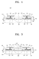
- FIG. 1 is a cross-sectional view exemplifying a semiconductor chip to which a cap wafer in accordance with an exemplary embodiment of the present invention is applied.
- the semiconductor chip 100 in accordance with an exemplary embodiment of the present invention includes a base wafer 150, a cap wafer 110, a cavity 120, and a bonding part 170.
- the base wafer 150 has circuit elements formed in the middle of an upper surface of a base wafer substrate 151.
- Electrode pads 162 are disposed on both sides of circuit elements 160, and are electrically coupled with leads (not illustrated) of the circuit elements 160.
- the electrode pads 162 are formed so as to correspond to a number of leads of the circuit elements 160.
- First sealing pads 163 are formed on the base wafer substrate 151 outside the electrode pads 162. Each of the first sealing pads 163 acts as a gasket for sealing the circuit elements when the cap wafer 110 and the base wafer 150 are bonded with each other.
- the electrode pads 162 and the first sealing pads 163 are formed of the same conductive material.
- the cap wafer 110 which is bonded with the base wafer 150 to package the circuit elements 160, includes a cap wafer substrate 111, penetrated electrodes 112, upper electrode pads 115, lower electrode pads 116, and second sealing pads 117.
- the cap wafer substrate 111 may be formed of silicon, high resistivity silicon, ceramic, single crystal ceramic, glass, or the like.
- the penetrated electrodes 112 are formed so that they penetrate the cap wafer substrate 111 over the electrode pads 162 of the base wafer 150, respectively.
- Each of the penetrated electrodes 112 has an oblique section, which gradually widens from an upper surface to a lower surface of the cap wafer substrate 111.
- Such penetrated electrodes 112 can be formed in a method which processes or machines one surface, that is, a lower surface, of the cap wafer substrate 111 with a dry etching process, a wet etching process, a sand blasting process, or a laser drilling process to form the sloped or oblique-via holes 113, and then fills the oblique-via holes 113 with conductive material through a plating process, which will be described below with reference to FIGS. 2A through 2D.
- the penetrated electrodes 112 are formed to have the oblique section in order that in a case of the oblique-via holes 113, the plating process of depositing a seed metal and filling the oblique-via holes 113 with a conductive material in forming the penetrated electrodes 112 is more easy performed as compared with related art straight-via holes. That is, the oblique-via holes 113 can form the penetrated electrodes 112 without generating defects, such as gaps or voids in the plating process. Also, the oblique-via holes 113 have a processing or machining amount, and/or a processing or machining time smaller than that of the straight-via holes. Accordingly, a working time can be reduced and thus fabrication costs can be reduced.
- the penetrated electrodes 112 are formed according to a number of the electrode pads 162 of the base wafer 150, that is, the number that corresponds to the number of the leads of the circuit elements 160.
- the upper electrode pads 115 are formed on upper parts of the penetrated electrodes 112, and are electrically coupled with an outer circuit (not shown).
- the lower electrode pads 116 are formed on under parts of the penetrated electrodes 112, and are electrically coupled with leads of the circuit elements 160 through first and second pad bonding layers 164 and 118 of the bonding part 170 to be described layer and with the electrode pads 162 of the base wafer 150.
- the second sealing pads 117 are formed on a lower surface of the cap wafer substrate 111 outside the lower electrode pads 116. Like the first sealing pads 163 of the base wafer 150, each of the second sealing pads 117 acts as a gasket for sealing the circuit elements 160 when the cap wafer 110 and the base wafer 150 are bonded with each other.
- the lower electrode pads 116 and the second sealing pads 117 are formed of a same material.
- the cavity 120 provides a room in which the circuit elements 160 formed on the upper surface of the base wafer substrate 151 can be operated, and is a space defined by the lower electrode pads 116 of the cap wafer 110 and the first and the second pad bonding layers 164 and 118 of the bonding part 170 between the cap wafer 110 and the base wafer 150. Accordingly, a depth of the cavity 120 is determined by a thicknesses of the lower electrode pads 116 and the first and the second pad bonding layers 164 and 118.
- the cavity 120 can be configured to further include a subsidiary cavity 120' (see FIG. 3).
- the subsidiary cavity 120' may be made up of a recess 120a, which is formed in a certain depth and a certain area on the lower surface of the cap wafer substrate 111 so as to face the elements 160.
- the bonding part 170 which bonds the cap wafer substrate 111 and the base wafer substrate 151 with each other, includes first and second pad bonding layers 164 and 118, and first and second sealing layers 165 and 119.
- the first and the second pad bonding layers 164 and 118 are disposed on the electrode pads 162 of the base wafer 150 and the lower electrode pads 116 of the cap wafer 110, respectively, to electrically couple therebetween.
- a material, which is usable as the first and the second pad bonding layers 164 and 118, may be Au, Sn, In, Pb, Ag, Bi, Zn, Cu, or the like, or a compound thereof (for example, AuSn, or InSn).
- the first and the second sealing layers 165 and 119 are disposed on the first sealing pads 163 of the base wafer 150 and the second sealing pads 117 of the cap wafer 110, respectively, and act to close up the cavity 120 in the bond between the cap wafer 110 and the base wafer 150.
- the first and the second sealing layers 165 and 119 can be formed of a same material as that of the first and the second pad bonding layers 164 and 118.
- the base wafer 150 with the cap wafer 110, when a proper temperature and a proper pressure are applied to the first and the second pad bonding layers 164 and 118 and the first and the second sealing layers 165 and 119, the first and the second pad bonding layers 164 and 118 and the first and the second sealing layers 165 and 119 are bonded by reacting to each other, respectively. As a result, the cap wafer 110 and the base wafer 150 are bonded with each other, and thereby the semiconductor chip 110 in which the circuit elements 110 is packaged is fabricated.
- the cap wafer 110 of the semiconductor chip 100 has penetrated electrodes 112 with an oblique section. Accordingly, the oblique-via holes 113 can be used when the penetrated electrodes 112 are formed. Thus, even though the penetrated electrodes 112 are formed in a high aspect ratio to reduce the semiconductor chip 100 in size, the oblique-via holes 113 can be easily formed, and a plating process for filling in the oblique-via holes 113 can be quickly carried out without generating defects, such as gaps or voids.
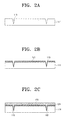
- a cap wafer substrate 111 which has a thickness larger than that of a cap wafer 110 to be finally formed, is prepared. Subsequently, as illustrated in FIG. 2A, oblique-via holes 113 are formed on a surface of the cap wafer substrate 111, which will form a lower surface of the cap wafer 110, by a dry etching method, a wet etching method, a sand blasting method, a laser drilling method, or the like.
- the oblique-via holes 113 are formed to have a wedge-shaped oblique section, which is gradually narrowed from the one surface to another surface (that is, from a lower surface to an upper surface) of the cap wafer substrate 111, and not to completely penetrate the cap wafer substrate 111.
- a seed later 121 is formed on an entire area of the surface of the cap wafer substrate 111 on which the oblique-via holes 113 are formed.
- the seed layer 121 which acts as a seed in a plating process to be described later, is made up of a conductive material, such as a metal.
- the surface of the cap wafer substrate 111 is exposed to a plating solution.
- a conductive substance is plated on the seed layer 121 to form a plated layer 123, which fills in the oblique-via holes 113.
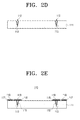
- the seed layer 121 and the plated layer 123 formed on the surface of the cap wafer substrate 111 are polished and removed. As a result, as illustrated in FIG. 2D, only portions of the seed layer 121 and the plated layer 123 which fills in the oblique-via holes 113, that is, penetrated electrodes 112 of the cap wafer 110, remain on the surface of the cap wafer substrate 111.
- first electrode layer can be formed of a conductive material, such as a metal
- the sealing layer can be formed of Au, Sn, In, Pb, Ag, Bi, Zn, Cu, or the like, or a compound thereof (for example, AuSn or InSn).
- the first electrode layer and the sealing layer are etched in a pattern.
- the pattern may be predetermined.
- the lower electrode pads 116, the second sealing pads 117, the second pad bonding layers 118 and the second sealing layers 119 are formed on the surface of the cap wafer substrate 111.
- a thickness of the lower electrode pads 116 or the second sealing pads 117 and the second pad bonding layers 118 or the second sealing layers 119 sets a depth of a cavity 120 in which the circuit elements 160 can operate, together with a thickness of first bonding layers 164 or first sealing layers 165 of a base wafer 160.
- the sum of the thicknesses of the lower electrode pads 116 or the second sealing pads 117 and the second pad bonding layers 118 or the second sealing layers 119 and the thickness of first bonding layers 164 or first sealing layers 165 is smaller than the depth of the cavity 120 needed for smoothly operating the circuit elements 160, it is advantageous if a subsidiary cavity 120' is formed to increase the depth of the cavity 120.
- the subsidiary cavity 120' can be formed by a dry etching method, a wet etching method, a san blasting method, a laser drilling method, or the like, after the penetrated electrodes 112 of the cap wafer 110 (FIG. 2C) are formed, or when the first electrode layer and the sealing layer are etched in the pattern to form the lower electrode pads 116, the second sealing pads 117, the second pad bonding layers 118 and the second sealing layers 119.
- the subsidiary cavity 102' may be a recess 120a, which is formed in to a certain depth and a certain area on the one surface of the cap wafer substrate 111 to face the circuit elements 160.
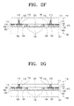
- the cap wafer substrate 110 is disposed, so that the second pad bonding layers 118 and the second sealing layers 119 face the first pad bonding layers 164 and the first sealing layers 165 of the separately formed base wafer 150. Subsequently, the second pad bonding layers 118 and the second sealing layers 119 are bonded with the first pad bonding layers 164 and the first sealing layers 165, respectively.
- the bonding method can use a method of applying a temperature and a pressure.
- the other surface, that is, an upper surface, of the cap wafer substrate 111 is thinned through a polishing process or an etching process. As a result, as illustrated in FIG. 2G, top parts of the penetrated electrodes 112 are exposed to the outside.
- the cap wafer 110 are formed by thinning the cap wafer substrate 111 with a thickness thicker than that thereof to be finally formed after it is bonded to the base wafer 150 in a state that the penetrated electrodes 112 are formed therein. Accordingly, the cap wafer 110 can be formed to have a reduced thickness without generating wafer damage which may occur in fabricating the cap wafer with a thin wafer. Also, damage of the circuit elements in the base wafer which occur in forming the penetrated electrodes after the bond between the cap wafer and the base wafer can be prevented.
- a second electrode layer (not illustrated) is formed on the upper surface of the cap wafer substrate 111.
- the second electrode layer can be formed of a conductive material.
- the second electrode layer is etched in a pattern.
- the upper electrode pads 115 are formed on the upper surface of the cap wafer substrate 111, and the fabrication process of the semiconductor chip 100 is completed.
- the cap wafer, the semiconductor chip having the same and a fabrication method thereof form the penetrated electrodes using the oblique-via holes. Accordingly, even though the penetrated electrodes are formed in the high aspect ratio to reduce the semiconductor chip in size, the via holes can be easily formed. Also, the plating process for filling in the via holes can be quickly carried out without generating defects, such as the gaps or the voids. Thus, a fabrication yield is increased and the fabrication costs are reduced.
- the cap wafer, the semiconductor chip having the same and the fabrication method thereof according to exemplary embodiments of the present invention reduce the thickness of the cap wafer by thinning the cap wafer. Accordingly, the semiconductor chip, which is finally formed, can be decreased in size.
- the cap wafer, the semiconductor chip having the same and the fabrication method thereof form the penetrated electrodes prior to bonding the cap wafer and the base wafer with each other. Accordingly, damage of the circuit elements in the base wafer which may occur in forming the penetrated electrode after the bond between the cap wafer and the base wafer can be prevented.
- the cap wafer and the base wafer can be simultaneously fabricated going side by side, thereby reducing a fabrication time.
- the cap wafer, the semiconductor chip having the same and the fabrication method thereof according to exemplary embodiments of the present invention thin the cap wafer after bonding the cap wafer to the base wafer. Accordingly, the cap wafer can be fabricated using the sufficiently thick wafer, thereby preventing wafer damage which may occur in fabricating the cap wafer with the thin wafer.
Landscapes
- Engineering & Computer Science (AREA)
- Microelectronics & Electronic Packaging (AREA)
- Computer Networks & Wireless Communication (AREA)
- Signal Processing (AREA)
- Computer Hardware Design (AREA)
- Internal Circuitry In Semiconductor Integrated Circuit Devices (AREA)
- Pressure Sensors (AREA)
Abstract
Description
- Apparatuses and methods consistent with the present invention relate to a cap wafer for packaging circuit elements formed on a base wafer, a semiconductor chip having the same, and a fabrication method thereof.
- Generally, a semiconductor chip, which is used in various electronic products, such as, for example, televisions, personal data assistants, mobile phones, etc., receives electric power from the outside to carry out a specific operation. Also, since the semiconductor chip has delicate electronic circuits built therein, it can be easily damaged by external impacts.
- Accordingly, in fabrication, the semiconductor chip essentially requires a packaging process, which electrically connects the electronic circuits therein to the outside and at the same time, hermetically packages them to withstand external impacts, thereby allowing the semiconductor chip to have a physical function and shape.
- As an example of techniques used in the packaging process, a wafer level packaging technique, which bonds a cap wafer having a shape to a base wafer in which circuit elements are formed, are known. The wafer level packaging technique is used as a packaging technique to satisfy reduced weight, decreased size and enhanced performance requirements of the electronic products, and is actively researched and developed in the semiconductor and micro electro mechanical system (MEMS) technology areas.
- However, due to a demand of reducing the electronic products in size according to the reduced weight, the decreased size and the enhanced performance thereof, the semiconductor chip fabricated using the wafer level packaging technique is designed so that penetrated electrodes formed in the cap wafer are maximally reduced in size. As a result, the penetrated electrodes are formed so that aspect ratios thereof are enlarged. If the aspect ratios of the penetrated electrodes come large, it is not easy to form straight-via holes for forming the penetrated electrodes during fabrication. Also, even though the straight-via holes are formed, it is difficult to deposit a seed layer on side surfaces of the straight-via holes, and to completely fill the straight-via holes with a conductive material due to a difference of plating speed between an upper surface of the cap wafer and the insides of the straight-via holes, and a difference of plating speed according to depths of the straight-via holes. As a result, gaps or voids may occur in the resultant penetrated electrodes. If the gaps occur, fine dusts may go into the semiconductor chip through the gaps. As a result, the chip may malfunction due to the dusts that came in through the gaps. Also, if the voids occur, impurities in the voids may be oxidized, and thereby the chip may malfunction or suffer damage in operation.
- To address the above problems, as a method of reducing the semiconductor chip in size, a method of forming the penetrated electrodes in a cap wafer with a decreased thickness can be considered. In this case, however, there is a limit to how far the thickness of the cap wafer may be reduced. This is because, in order to increase productivity, a size of wafer for forming the cap wafer is gradually increasing. Thus, a thickness of wafer, which can be fabricated without resulting in a wafer damage in a chip fabrication, is restricted.
- As another method of reducing the semiconductor chip in size, a method of joining a sufficiently thick cap wafer with a base wafer, thinning an upper surface of the cap wafer to reduce the thickness of the cap wafer and then forming the penetrated electrodes in the cap wafer, can be considered. In this case, the above problem that the wafer is damaged due to the decreased thickness in the chip fabrication may be addressed. However, a problem occurs in that circuit elements of the base wafer are often damaged in forming the penetrated electrodes. Also, the method does not simultaneously form the cap wafer and the base wafer, but should form the base wafer prior to forming the cap wafer. Accordingly, a problem occurs in that a chip fabrication time is lengthened.
- Thus, it would be advantageous to have a new fabrication method of the semiconductor chip which does not generate the above problems, even though the penetrated electrodes are formed in a high aspect ratio or the thickness of the cap wafer is decreased to reduce the semiconductor chip in size.
- Exemplary embodiments of the present invention overcome the above disadvantages and other disadvantages not described above. Also, the present invention is not required to overcome the disadvantages described above, and an exemplary embodiment of the present invention may not overcome any of the problems described above.
- Accordingly, an aspect of the present invention is to provide a cap wafer in which penetrated electrodes have oblique sections, so that even though they are designed in a high aspect ratio to reduce a size of the semiconductor chip, the chip wafer may be easily and quickly fabricated, thereby reducing fabrication costs, and a semiconductor chip having the same, and a fabrication method thereof.
- Another aspect of the present invention is to provide a cap wafer having a reduced thickness to decrease a size of the semiconductor chip, a semiconductor chip having the same, and a fabrication method thereof.
- Still another aspect of the present invention is to provide a fabrication method of a cap wafer and a fabrication method of a semiconductor chip in which penetrated electrodes are formed in a cap wafer prior to bonding the cap wafer and a base wafer with each other, so that damage of circuit elements in the base wafer can be prevented from occurring in forming the penetrated electrode after the bond between the cap wafer and the base wafer, and also so the cap wafer and the base wafer can be simultaneously fabricated, thereby reducing a fabrication time.
- Another aspect of the present invention is to provide a fabrication method of a semiconductor chip in which a cap wafer is thinned after bonding the cap wafer to a base wafer, so that the cap wafer can be fabricated using a sufficiently thick wafer, thereby preventing wafer damage from occurring in fabricating the cap wafer with a thin wafer.
- Additional aspects of the invention will be set forth in part in the description which follows and, in part, will be obvious from the description, or may be learned by practice of the invention.
- According to an aspect of the present invention, there is provided a cap wafer including a cap wafer substrate, at least one penetrated electrode formed to penetrate the cap wafer substrate, and at least one electrode pad connected with a lower portion of the penetrated electrode on a lower surface of the cap wafer substrate. The penetrated electrode has an oblique section which gradually widens from an upper surface to the lower surface of the cap wafer substrate.
- The penetrated electrode may be completely filled in an oblique-via hole formed to penetrate the cap wafer substrate and to have an oblique section.
- Alternatively, the cap wafer may further include a subsidiary cavity formed on the lower surface of the cap wafer substrate.
- According to another aspect of the present invention, there is provided a fabrication method of a cap wafer, including forming at least one oblique-via hole on a lower surface of a cap wafer substrate, the oblique-via hole having an oblique section which gradually narrows in a direction moving away from the lower surface of the cap wafer substrate, and forming a penetrated electrode in the oblique-via hole.
- At the forming the oblique-via hole, the oblique-via hole may be formed so as not to completely penetrate the cap wafer substrate. Also, the oblique-via hole may be formed by one of a dry etching, a wet etching, a sand blasting, and a laser drilling.
- The forming the penetrated electrode may be carried out by forming a seed layer on an entire area of the lower surface of the cap wafer substrate on which the oblique-via hole is formed, plating an entire area of the one surface of the cap wafer substrate on which the seed layer is formed, and polishing the surface of the cap wafer substrate.
- Further, the fabrication method may further include forming at least one electrode pad coming in contact with the penetrated electrode on the surface of the cap wafer substrate after the forming the penetrated electrode.
- Also, alternatively, the fabrication method may further include forming a subsidiary cavity on the surface of the cap wafer substrate after the forming the penetrated electrode.
- According to still another aspect of the present invention, there is provided a semiconductor chip, including a base wafer which has at least one circuit element on an upper surface thereof, a cap wafer which is bonded with the base wafer to package the circuit element, a cavity which is located between the circuit element and a lower surface of the cap wafer, at least one penetrated electrode which is formed to penetrate the cap wafer and has an oblique section which gradually widens from an upper surface to the lower surface of the cap wafer, and at least one pad bonding layer which electrically couples the penetrated electrode to the circuit element.
- The penetrated electrode may be completely filled in an oblique-via hole formed to penetrate a cap wafer substrate of the cap wafer and to have the oblique section.
- The cavity may be a space set by the pad bonding layer between the cap wafer and the base wafer. Alternatively, the cavity may further include a subsidiary cavity comprising a recess formed on a lower surface of a cap wafer substrate of the cap wafer.
- According to other aspect of the present invention, there is provided a fabrication method of a semiconductor chip, including: preparing a base wafer having at least one circuit element on a surface thereof, preparing a cap wafer having at least one penetrated electrode exposed to the outside through a surface thereof, bonding the surface of the base wafer and the surface of the cap wafer with each other, and thinning another surface of the cap wafer to expose the penetrated electrode to the outside therethrough.
- The preparing the cap wafer may be carried out by forming at least one oblique-via hole with an oblique section on a surface of a cap wafer substrate of the cap wafer, and forming a penetrated electrode in the oblique-via hole.
- The forming the oblique-via hole may be carried out by forming an oblique-via hole having an oblique section which gradually narrows in a direction moving away from the surface of the cap wafer substrate. The oblique-via hole may be formed so as not to completely penetrate the cap wafer substrate. Also, the oblique-via hole may be formed by one of a dry etching, a wet etching, a sand blasting, and a laser drilling.
- The forming the penetrated electrode may be carried out by forming a seed layer on an entire area of the surface of the cap wafer substrate on which the oblique-via hole is formed, plating an entire area of the surface of the cap wafer substrate on which the seed layer is formed, and polishing the surface of the cap wafer substrate.
- The preparing the cap wafer may further include forming at least one electrode pad which comes in contact with the penetrated electrode on the surface of the cap wafer substrate after the forming the penetrated electrode.
- Also, the preparing the cap wafer may further include forming a subsidiary cavity on the surface of the cap wafer substrate after the forming the penetrated electrode.
- The bonding the surface of the base wafer and the surface of the cap wafer may be carried out by bonding the surface of the base wafer and the surface of the cap wafer with each other by using at least one pad bonding layer and at least one sealing layer, the pad bonding layer electrically coupling the penetrated electrode to the circuit element and the sealing layer closing up a cavity between the base wafer and the cap wafer.
- The fabrication method may further include forming at least one electrode pad which couples the penetrated electrode to an outside on another surface of the cap wafer after the thinning the other surface of the cap wafer.
- The above aspects of the present invention will be more apparent from the description of exemplary embodiments of the present invention taken with reference to the accompanying drawings, in which:
- FIG. 1 is a cross-sectional view exemplifying a semiconductor chip in accordance with an exemplary embodiment of the present invention;
- FIGS. 2A through 2G are cross-sectional views exemplifying a fabrication method of the semiconductor chip illustrated in FIG. 1; and
- FIG. 3 is a cross-sectional view exemplifying a semiconductor chip in accordance with another exemplary embodiment of the present invention.
- Throughout the drawings, the same drawing reference numerals will be understood to refer to the same elements, features, and structures.
- Reference will now be made in detail to exemplary embodiments of the present invention, which are illustrated in the accompanying drawings.
- FIG. 1 is a cross-sectional view exemplifying a semiconductor chip to which a cap wafer in accordance with an exemplary embodiment of the present invention is applied.
- Referring to FIG. 1, the
semiconductor chip 100 in accordance with an exemplary embodiment of the present invention includes abase wafer 150, acap wafer 110, acavity 120, and abonding part 170. - The
base wafer 150 has circuit elements formed in the middle of an upper surface of abase wafer substrate 151. -
Electrode pads 162 are disposed on both sides ofcircuit elements 160, and are electrically coupled with leads (not illustrated) of thecircuit elements 160. Theelectrode pads 162 are formed so as to correspond to a number of leads of thecircuit elements 160. - First sealing
pads 163 are formed on thebase wafer substrate 151 outside theelectrode pads 162. Each of thefirst sealing pads 163 acts as a gasket for sealing the circuit elements when thecap wafer 110 and thebase wafer 150 are bonded with each other. - The
electrode pads 162 and thefirst sealing pads 163 are formed of the same conductive material. - The
cap wafer 110, which is bonded with thebase wafer 150 to package thecircuit elements 160, includes acap wafer substrate 111, penetratedelectrodes 112,upper electrode pads 115,lower electrode pads 116, andsecond sealing pads 117. - The
cap wafer substrate 111 may be formed of silicon, high resistivity silicon, ceramic, single crystal ceramic, glass, or the like. - The penetrated
electrodes 112 are formed so that they penetrate thecap wafer substrate 111 over theelectrode pads 162 of thebase wafer 150, respectively. Each of the penetratedelectrodes 112 has an oblique section, which gradually widens from an upper surface to a lower surface of thecap wafer substrate 111. Such penetratedelectrodes 112 can be formed in a method which processes or machines one surface, that is, a lower surface, of thecap wafer substrate 111 with a dry etching process, a wet etching process, a sand blasting process, or a laser drilling process to form the sloped or oblique-viaholes 113, and then fills the oblique-viaholes 113 with conductive material through a plating process, which will be described below with reference to FIGS. 2A through 2D. - The penetrated
electrodes 112 are formed to have the oblique section in order that in a case of the oblique-viaholes 113, the plating process of depositing a seed metal and filling the oblique-viaholes 113 with a conductive material in forming the penetratedelectrodes 112 is more easy performed as compared with related art straight-via holes. That is, the oblique-viaholes 113 can form the penetratedelectrodes 112 without generating defects, such as gaps or voids in the plating process. Also, the oblique-viaholes 113 have a processing or machining amount, and/or a processing or machining time smaller than that of the straight-via holes. Accordingly, a working time can be reduced and thus fabrication costs can be reduced. - Also, the penetrated
electrodes 112 are formed according to a number of theelectrode pads 162 of thebase wafer 150, that is, the number that corresponds to the number of the leads of thecircuit elements 160. - The
upper electrode pads 115 are formed on upper parts of the penetratedelectrodes 112, and are electrically coupled with an outer circuit (not shown). - The
lower electrode pads 116 are formed on under parts of the penetratedelectrodes 112, and are electrically coupled with leads of thecircuit elements 160 through first and second pad bonding layers 164 and 118 of thebonding part 170 to be described layer and with theelectrode pads 162 of thebase wafer 150. - The
second sealing pads 117 are formed on a lower surface of thecap wafer substrate 111 outside thelower electrode pads 116. Like thefirst sealing pads 163 of thebase wafer 150, each of thesecond sealing pads 117 acts as a gasket for sealing thecircuit elements 160 when thecap wafer 110 and thebase wafer 150 are bonded with each other. - The
lower electrode pads 116 and thesecond sealing pads 117 are formed of a same material. - The
cavity 120 provides a room in which thecircuit elements 160 formed on the upper surface of thebase wafer substrate 151 can be operated, and is a space defined by thelower electrode pads 116 of thecap wafer 110 and the first and the second pad bonding layers 164 and 118 of thebonding part 170 between thecap wafer 110 and thebase wafer 150. Accordingly, a depth of thecavity 120 is determined by a thicknesses of thelower electrode pads 116 and the first and the second pad bonding layers 164 and 118. - If the thicknesses of the
lower electrode pads 116 and the first and the second pad bonding layers 164 and 118 is too small to provide room in which thecircuit elements 160 can be smoothly operated, thecavity 120 can be configured to further include a subsidiary cavity 120' (see FIG. 3). The subsidiary cavity 120' may be made up of arecess 120a, which is formed in a certain depth and a certain area on the lower surface of thecap wafer substrate 111 so as to face theelements 160. - The
bonding part 170, which bonds thecap wafer substrate 111 and thebase wafer substrate 151 with each other, includes first and second pad bonding layers 164 and 118, and first and second sealing layers 165 and 119. - The first and the second pad bonding layers 164 and 118 are disposed on the
electrode pads 162 of thebase wafer 150 and thelower electrode pads 116 of thecap wafer 110, respectively, to electrically couple therebetween. A material, which is usable as the first and the second pad bonding layers 164 and 118, may be Au, Sn, In, Pb, Ag, Bi, Zn, Cu, or the like, or a compound thereof (for example, AuSn, or InSn). - The first and the second sealing layers 165 and 119 are disposed on the
first sealing pads 163 of thebase wafer 150 and thesecond sealing pads 117 of thecap wafer 110, respectively, and act to close up thecavity 120 in the bond between thecap wafer 110 and thebase wafer 150. The first and the second sealing layers 165 and 119 can be formed of a same material as that of the first and the second pad bonding layers 164 and 118. - Accordingly, to package the
base wafer 150 with thecap wafer 110, when a proper temperature and a proper pressure are applied to the first and the second pad bonding layers 164 and 118 and the first and the second sealing layers 165 and 119, the first and the second pad bonding layers 164 and 118 and the first and the second sealing layers 165 and 119 are bonded by reacting to each other, respectively. As a result, thecap wafer 110 and thebase wafer 150 are bonded with each other, and thereby thesemiconductor chip 110 in which thecircuit elements 110 is packaged is fabricated. - As described above, the
cap wafer 110 of thesemiconductor chip 100 according to an exemplary embodiment of the present invention has penetratedelectrodes 112 with an oblique section. Accordingly, the oblique-viaholes 113 can be used when the penetratedelectrodes 112 are formed. Thus, even though the penetratedelectrodes 112 are formed in a high aspect ratio to reduce thesemiconductor chip 100 in size, the oblique-viaholes 113 can be easily formed, and a plating process for filling in the oblique-viaholes 113 can be quickly carried out without generating defects, such as gaps or voids. - Hereinafter, a fabrication process of a
semiconductor chip 100 constructed as described above will be described in details with reference to FIGS. 1 through 2G. - A
cap wafer substrate 111, which has a thickness larger than that of acap wafer 110 to be finally formed, is prepared. Subsequently, as illustrated in FIG. 2A, oblique-viaholes 113 are formed on a surface of thecap wafer substrate 111, which will form a lower surface of thecap wafer 110, by a dry etching method, a wet etching method, a sand blasting method, a laser drilling method, or the like. The oblique-viaholes 113 are formed to have a wedge-shaped oblique section, which is gradually narrowed from the one surface to another surface (that is, from a lower surface to an upper surface) of thecap wafer substrate 111, and not to completely penetrate thecap wafer substrate 111. - As illustrated in FIG. 2B, a seed later 121 is formed on an entire area of the surface of the
cap wafer substrate 111 on which the oblique-viaholes 113 are formed. Theseed layer 121, which acts as a seed in a plating process to be described later, is made up of a conductive material, such as a metal. - The surface of the
cap wafer substrate 111 is exposed to a plating solution. As a result, as illustrated in FIG. 2C, a conductive substance is plated on theseed layer 121 to form a platedlayer 123, which fills in the oblique-viaholes 113. - The
seed layer 121 and the platedlayer 123 formed on the surface of thecap wafer substrate 111 are polished and removed. As a result, as illustrated in FIG. 2D, only portions of theseed layer 121 and the platedlayer 123 which fills in the oblique-viaholes 113, that is, penetratedelectrodes 112 of thecap wafer 110, remain on the surface of thecap wafer substrate 111. - To form
lower electrode pads 116,second sealing pads 117, second pad bonding layers 118 and second sealing layers 119, a first electrode layer (not illustrated) and a first sealing layer (not illustrated) are formed in turn on the surface of thecap wafer substrate 111. The first electrode layer can be formed of a conductive material, such as a metal, and the sealing layer can be formed of Au, Sn, In, Pb, Ag, Bi, Zn, Cu, or the like, or a compound thereof (for example, AuSn or InSn). - The first electrode layer and the sealing layer are etched in a pattern. The pattern may be predetermined. As a result, as illustrated in FIG. 2E, the
lower electrode pads 116, thesecond sealing pads 117, the second pad bonding layers 118 and the second sealing layers 119 are formed on the surface of thecap wafer substrate 111. - When a
base wafer 150 is packaged with thecap wafer 110 later, a thickness of thelower electrode pads 116 or thesecond sealing pads 117 and the second pad bonding layers 118 or the second sealing layers 119 sets a depth of acavity 120 in which thecircuit elements 160 can operate, together with a thickness of first bonding layers 164 or first sealing layers 165 of abase wafer 160. Thus, if the sum of the thicknesses of thelower electrode pads 116 or thesecond sealing pads 117 and the second pad bonding layers 118 or the second sealing layers 119 and the thickness of first bonding layers 164 or first sealing layers 165 is smaller than the depth of thecavity 120 needed for smoothly operating thecircuit elements 160, it is advantageous if a subsidiary cavity 120' is formed to increase the depth of thecavity 120. The subsidiary cavity 120' can be formed by a dry etching method, a wet etching method, a san blasting method, a laser drilling method, or the like, after the penetratedelectrodes 112 of the cap wafer 110 (FIG. 2C) are formed, or when the first electrode layer and the sealing layer are etched in the pattern to form thelower electrode pads 116, thesecond sealing pads 117, the second pad bonding layers 118 and the second sealing layers 119. The subsidiary cavity 102' may be arecess 120a, which is formed in to a certain depth and a certain area on the one surface of thecap wafer substrate 111 to face thecircuit elements 160. - As illustrated in FIG. 2F, the
cap wafer substrate 110 is disposed, so that the second pad bonding layers 118 and the second sealing layers 119 face the first pad bonding layers 164 and the first sealing layers 165 of the separately formedbase wafer 150. Subsequently, the second pad bonding layers 118 and the second sealing layers 119 are bonded with the first pad bonding layers 164 and the first sealing layers 165, respectively. The bonding method can use a method of applying a temperature and a pressure. - The other surface, that is, an upper surface, of the
cap wafer substrate 111 is thinned through a polishing process or an etching process. As a result, as illustrated in FIG. 2G, top parts of the penetratedelectrodes 112 are exposed to the outside. - As described above, the
cap wafer 110 according to exemplary embodiments of the present invention are formed by thinning thecap wafer substrate 111 with a thickness thicker than that thereof to be finally formed after it is bonded to thebase wafer 150 in a state that the penetratedelectrodes 112 are formed therein. Accordingly, thecap wafer 110 can be formed to have a reduced thickness without generating wafer damage which may occur in fabricating the cap wafer with a thin wafer. Also, damage of the circuit elements in the base wafer which occur in forming the penetrated electrodes after the bond between the cap wafer and the base wafer can be prevented. - To form
upper electrode pads 115 to be connected to an outer circuit, a second electrode layer (not illustrated) is formed on the upper surface of thecap wafer substrate 111. The second electrode layer can be formed of a conductive material. - The second electrode layer is etched in a pattern. As a result, as illustrated in FIG. 1, the
upper electrode pads 115 are formed on the upper surface of thecap wafer substrate 111, and the fabrication process of thesemiconductor chip 100 is completed. - As apparent from the foregoing description, according to exemplary embodiments of the present invention, the cap wafer, the semiconductor chip having the same and a fabrication method thereof form the penetrated electrodes using the oblique-via holes. Accordingly, even though the penetrated electrodes are formed in the high aspect ratio to reduce the semiconductor chip in size, the via holes can be easily formed. Also, the plating process for filling in the via holes can be quickly carried out without generating defects, such as the gaps or the voids. Thus, a fabrication yield is increased and the fabrication costs are reduced.
- Further, the cap wafer, the semiconductor chip having the same and the fabrication method thereof according to exemplary embodiments of the present invention reduce the thickness of the cap wafer by thinning the cap wafer. Accordingly, the semiconductor chip, which is finally formed, can be decreased in size.
- Also, the cap wafer, the semiconductor chip having the same and the fabrication method thereof according to exemplary embodiments of the present invention form the penetrated electrodes prior to bonding the cap wafer and the base wafer with each other. Accordingly, damage of the circuit elements in the base wafer which may occur in forming the penetrated electrode after the bond between the cap wafer and the base wafer can be prevented. The cap wafer and the base wafer can be simultaneously fabricated going side by side, thereby reducing a fabrication time.
- Moreover, the cap wafer, the semiconductor chip having the same and the fabrication method thereof according to exemplary embodiments of the present invention thin the cap wafer after bonding the cap wafer to the base wafer. Accordingly, the cap wafer can be fabricated using the sufficiently thick wafer, thereby preventing wafer damage which may occur in fabricating the cap wafer with the thin wafer.
- Although exemplary embodiments of the present invention have been shown and described, it will be appreciated by those skilled in the art that changes may be made in these exemplary embodiments without departing from the scope of the invention which is defined in the claims.
Claims (21)
- A cap wafer (110) comprising:a cap wafer substrate (111);at least one penetrated electrode (112) formed to penetrate the cap wafer substrate; andat least one electrode pad (116) connected with a lower portion of the penetrated electrode on a lower surface of the cap wafer substrate (110),wherein the penetrated electrode (112) has an oblique section which gradually widens from an upper surface to the lower surface of the cap wafer substrate.
- The cap wafer as claimed in claim 1, wherein the penetrated electrode is completely filled in an oblique-via hole formed to penetrate the cap wafer substrate and to have an oblique section.
- The cap wafer as claimed in claim 1 or 2, further comprising a subsidiary cavity formed on the lower surface of the cap wafer substrate.
- A semiconductor chip comprising:a base wafer (150) which has at least one circuit element (160) on an upper surface thereof;a cap wafer (110) as claimed in any preceding claim, which bonds with the base wafer (150) to package the circuit element,wherein a cavity is located between the circuit element (160) and the lower surface of the cap wafer,
and wherein the chip comprises at least one pad bonding layer (118,164) which electrically couples the penetrated electrode to the circuit element (160). - The semiconductor chip as claimed in claim 4, wherein the cavity comprises a space defined by the pad bonding layer between the cap wafer and the base wafer.
- A fabrication method of a cap wafer, the method comprising:forming at least one oblique-via hole on a lower surface of a cap wafer substrate, the oblique-via hole having an oblique section which gradually narrows in a direction moving away from the lower surface of the cap wafer substrate; andforming a penetrated electrode in the oblique-via hole.
- The fabrication method as claimed in claim 6, wherein in the forming the at least one oblique-via hole, the oblique-via hole is formed so as not to completely penetrate the cap wafer substrate.
- The fabrication method as claimed in claim 6 or 7, wherein the oblique-via hole is formed by one of a dry etching, a wet etching, a sand blasting, and a laser drilling.
- The fabrication method as claimed in any one of claims 6 to 8, wherein the forming the penetrated electrode comprises:forming a seed layer on an entire area of the lower surface of the cap wafer substrate on which the oblique-via hole is formed;plating an entire area of the lower surface of the cap wafer substrate on which the seed layer is formed; andpolishing the lower surface of the cap wafer substrate.
- The fabrication method as claimed in any one of claims 6 to 9, further comprising:after the forming the penetrated electrode, forming at least one electrode pad which contacts the penetrated electrode on the lower surface of the cap wafer substrate.
- The fabrication method as claimed in any one of claims 6 to 10, further comprising:after the forming the penetrated electrode, forming a subsidiary cavity on the lower surface of the cap wafer substrate.
- A fabrication method of a semiconductor chip, the method comprising:preparing a base wafer having at least one circuit element on a surface thereof;preparing a cap wafer having at least one penetrated electrode exposed to the outside of the cap wafer through a first surface thereof;bonding the surface of the base wafer and the surface of the cap wafer with each other; andthinning a second surface of the cap wafer to expose the penetrated electrode to the outside therethrough.
- The fabrication method as claimed in claim 12, wherein the preparing the cap wafer comprises:forming at least one oblique-via hole with an oblique section on a surface of a cap wafer substrate of the cap wafer; andforming a penetrated electrode in the oblique-via hole.
- The fabrication method as claimed in claim 13, wherein the forming the at least one oblique-via hole comprises forming an oblique-via hole having an oblique section which gradually narrows in a direction moving away from the surface of the cap wafer substrate.
- The fabrication method as claimed in claim 14, wherein the oblique-via hole is formed so as not to completely penetrate the cap wafer substrate.
- The fabrication method as claimed in claim 14 or 15, wherein the oblique-via hole is formed by one of a dry etching, a wet etching, a sand blasting, and a laser drilling.
- The fabrication method as claimed in any one of claims 12 to 16, wherein the forming the penetrated electrode comprises:forming a seed layer on an entire area of the surface of the cap wafer substrate on which the oblique-via hole is formed;plating an entire area of the surface of the cap wafer substrate on which the seed layer is formed; andpolishing the surface of the cap wafer substrate.
- The fabrication method as claimed in any one of claims 12 to 17, wherein the preparing the cap wafer further comprises, after the forming the penetrated electrode, forming at least one electrode pad which contacts the penetrated electrode on one surface of the cap wafer substrate.
- The fabrication method as claimed in any one of claims 12 to 18, wherein the preparing the cap wafer further comprises, after the forming the penetrated electrode, forming a subsidiary cavity on the surface of the cap wafer substrate.
- The fabrication method as claimed in any one of claims 12 to 19, wherein the bonding the surface of the base wafer and the surface of the cap wafer comprises:bonding the surface of the base wafer and the surface of the cap wafer with each other by using at least one pad bonding layer and at least one sealing layer, the at least one pad bonding layer electrically coupling the penetrated electrode to the circuit element and the sealing layer closing a cavity between the base wafer and the cap wafer.
- The fabrication method as claimed in any one of claims 12 to 20, further comprising:after the thinning the other surface of the cap wafer, forming at least one electrode pad which connects the penetrated electrode to the outside of the semiconductor chip on another surface of the cap wafer.
Applications Claiming Priority (1)
| Application Number | Priority Date | Filing Date | Title |
|---|---|---|---|
| KR1020060089815A KR100750741B1 (en) | 2006-09-15 | 2006-09-15 | Cap Wafer, Semiconductor Chip Having Same, and Manufacturing Method Thereof |
Publications (2)
| Publication Number | Publication Date |
|---|---|
| EP1900680A2 true EP1900680A2 (en) | 2008-03-19 |
| EP1900680A3 EP1900680A3 (en) | 2010-11-17 |
Family
ID=38537726
Family Applications (1)
| Application Number | Title | Priority Date | Filing Date |
|---|---|---|---|
| EP07115664A Withdrawn EP1900680A3 (en) | 2006-09-15 | 2007-09-04 | Cap wafer having electrodes |
Country Status (4)
| Country | Link |
|---|---|
| US (1) | US7626258B2 (en) |
| EP (1) | EP1900680A3 (en) |
| JP (1) | JP4789836B2 (en) |
| KR (1) | KR100750741B1 (en) |
Cited By (2)
| Publication number | Priority date | Publication date | Assignee | Title |
|---|---|---|---|---|
| WO2010059118A1 (en) * | 2008-11-19 | 2010-05-27 | Silex Microsystems Ab | Functional capping |
| WO2015030657A1 (en) | 2013-08-26 | 2015-03-05 | Silex Microsystems Ab | Thin capping for mems devices |
Families Citing this family (23)
| Publication number | Priority date | Publication date | Assignee | Title |
|---|---|---|---|---|
| US7791199B2 (en) | 2006-11-22 | 2010-09-07 | Tessera, Inc. | Packaged semiconductor chips |
| US8569876B2 (en) | 2006-11-22 | 2013-10-29 | Tessera, Inc. | Packaged semiconductor chips with array |
| WO2008108970A2 (en) | 2007-03-05 | 2008-09-12 | Tessera, Inc. | Chips having rear contacts connected by through vias to front contacts |
| WO2009017835A2 (en) | 2007-07-31 | 2009-02-05 | Tessera, Inc. | Semiconductor packaging process using through silicon vias |
| JP4784641B2 (en) * | 2008-12-23 | 2011-10-05 | 株式会社デンソー | Semiconductor device and manufacturing method thereof |
| US8482132B2 (en) * | 2009-10-08 | 2013-07-09 | International Business Machines Corporation | Pad bonding employing a self-aligned plated liner for adhesion enhancement |
| US10297550B2 (en) * | 2010-02-05 | 2019-05-21 | Taiwan Semiconductor Manufacturing Company, Ltd. | 3D IC architecture with interposer and interconnect structure for bonding dies |
| US8791575B2 (en) | 2010-07-23 | 2014-07-29 | Tessera, Inc. | Microelectronic elements having metallic pads overlying vias |
| US8796135B2 (en) | 2010-07-23 | 2014-08-05 | Tessera, Inc. | Microelectronic elements with rear contacts connected with via first or via middle structures |
| US9640437B2 (en) | 2010-07-23 | 2017-05-02 | Tessera, Inc. | Methods of forming semiconductor elements using micro-abrasive particle stream |
| US8343789B2 (en) * | 2010-08-17 | 2013-01-01 | Taiwan Semiconductor Manufacturing Company, Ltd. | Microstructure device with an improved anchor |
| US8610259B2 (en) | 2010-09-17 | 2013-12-17 | Tessera, Inc. | Multi-function and shielded 3D interconnects |
| US8847380B2 (en) | 2010-09-17 | 2014-09-30 | Tessera, Inc. | Staged via formation from both sides of chip |
| US8637968B2 (en) | 2010-12-02 | 2014-01-28 | Tessera, Inc. | Stacked microelectronic assembly having interposer connecting active chips |
| US8736066B2 (en) | 2010-12-02 | 2014-05-27 | Tessera, Inc. | Stacked microelectronic assemby with TSVS formed in stages and carrier above chip |
| US8587126B2 (en) | 2010-12-02 | 2013-11-19 | Tessera, Inc. | Stacked microelectronic assembly with TSVs formed in stages with plural active chips |
| US8610264B2 (en) | 2010-12-08 | 2013-12-17 | Tessera, Inc. | Compliant interconnects in wafers |
| KR20120077876A (en) | 2010-12-31 | 2012-07-10 | 삼성전자주식회사 | Heterojunction structures of different substrates joined and methods for fabricating the same |
| US9165792B2 (en) * | 2012-09-25 | 2015-10-20 | Infineon Technologies Ag | Integrated circuit, a chip package and a method for manufacturing an integrated circuit |
| US10629468B2 (en) | 2016-02-11 | 2020-04-21 | Skyworks Solutions, Inc. | Device packaging using a recyclable carrier substrate |
| US10453763B2 (en) | 2016-08-10 | 2019-10-22 | Skyworks Solutions, Inc. | Packaging structures with improved adhesion and strength |
| CN107764439B (en) * | 2016-08-19 | 2020-01-24 | 上海丽恒光微电子科技有限公司 | Preparation method of pressure sensor |
| CN108172553A (en) * | 2018-01-17 | 2018-06-15 | 杭州暖芯迦电子科技有限公司 | A kind of encapsulating structure and its packaging method of retina Using prosthesis chip |
Family Cites Families (16)
| Publication number | Priority date | Publication date | Assignee | Title |
|---|---|---|---|---|
| US5229647A (en) * | 1991-03-27 | 1993-07-20 | Micron Technology, Inc. | High density data storage using stacked wafers |
| US6228675B1 (en) * | 1999-07-23 | 2001-05-08 | Agilent Technologies, Inc. | Microcap wafer-level package with vias |
| KR100394808B1 (en) * | 2001-07-19 | 2003-08-14 | 삼성전자주식회사 | Wafer level stack chip package and method for manufacturing the same |
| JP2004129223A (en) * | 2002-07-31 | 2004-04-22 | Murata Mfg Co Ltd | Piezoelectric component and method of manufacturing the same |
| DE10393265T5 (en) * | 2002-09-13 | 2005-09-15 | Advantest Corp. | Micro device and method for its production |
| JP2004193297A (en) * | 2002-12-11 | 2004-07-08 | Dainippon Printing Co Ltd | Wafer level package and method of manufacturing the same |
| KR100512971B1 (en) * | 2003-02-24 | 2005-09-07 | 삼성전자주식회사 | Manufacturing method of micro electro mechanical system using solder ball |
| US6841883B1 (en) * | 2003-03-31 | 2005-01-11 | Micron Technology, Inc. | Multi-dice chip scale semiconductor components and wafer level methods of fabrication |
| US20040259325A1 (en) * | 2003-06-19 | 2004-12-23 | Qing Gan | Wafer level chip scale hermetic package |
| WO2005031862A1 (en) * | 2003-09-26 | 2005-04-07 | Tessera, Inc. | Structure and method of making sealed capped chips |
| JP2005109221A (en) * | 2003-09-30 | 2005-04-21 | Toshiba Corp | Wafer level package and manufacturing method thereof |
| US7109068B2 (en) * | 2004-08-31 | 2006-09-19 | Micron Technology, Inc. | Through-substrate interconnect fabrication methods |
| US7061099B2 (en) * | 2004-09-30 | 2006-06-13 | Intel Corporation | Microelectronic package having chamber sealed by material including one or more intermetallic compounds |
| JP2006173557A (en) * | 2004-11-22 | 2006-06-29 | Toshiba Corp | Hollow semiconductor device and manufacturing method thereof |
| US7449355B2 (en) * | 2005-04-27 | 2008-11-11 | Robert Bosch Gmbh | Anti-stiction technique for electromechanical systems and electromechanical device employing same |
| KR100731351B1 (en) * | 2006-02-01 | 2007-06-21 | 삼성전자주식회사 | Surface acoustic wave device wafer level package and its packaging method |
-
2006
- 2006-09-15 KR KR1020060089815A patent/KR100750741B1/en not_active Expired - Fee Related
-
2007
- 2007-01-24 US US11/657,056 patent/US7626258B2/en not_active Expired - Fee Related
- 2007-03-20 JP JP2007073057A patent/JP4789836B2/en not_active Expired - Fee Related
- 2007-09-04 EP EP07115664A patent/EP1900680A3/en not_active Withdrawn
Cited By (7)
| Publication number | Priority date | Publication date | Assignee | Title |
|---|---|---|---|---|
| WO2010059118A1 (en) * | 2008-11-19 | 2010-05-27 | Silex Microsystems Ab | Functional capping |
| US9362139B2 (en) | 2008-11-19 | 2016-06-07 | Silex Microsystems Ab | Method of making a semiconductor device having a functional capping |
| WO2015030657A1 (en) | 2013-08-26 | 2015-03-05 | Silex Microsystems Ab | Thin capping for mems devices |
| CN105916801A (en) * | 2013-08-26 | 2016-08-31 | 西雷克斯微系统股份有限公司 | Thin covers for MEMS devices |
| EP3038974A4 (en) * | 2013-08-26 | 2017-07-26 | Silex Microsystems AB | Thin capping for mems devices |
| US9718674B2 (en) | 2013-08-26 | 2017-08-01 | Silex Microsystems Ab | Thin capping for MEMS devices |
| CN105916801B (en) * | 2013-08-26 | 2017-10-10 | 西雷克斯微系统股份有限公司 | Thin covers for MEMS devices |
Also Published As
| Publication number | Publication date |
|---|---|
| JP4789836B2 (en) | 2011-10-12 |
| EP1900680A3 (en) | 2010-11-17 |
| JP2008072082A (en) | 2008-03-27 |
| KR100750741B1 (en) | 2007-08-22 |
| US7626258B2 (en) | 2009-12-01 |
| US20080067664A1 (en) | 2008-03-20 |
Similar Documents
| Publication | Publication Date | Title |
|---|---|---|
| US7626258B2 (en) | Cap wafer, semiconductor chip having the same, and fabrication method thereof | |
| US6710461B2 (en) | Wafer level packaging of micro electromechanical device | |
| JP5621155B2 (en) | Method for vertically interconnecting 3D electronic modules by vias | |
| KR100851931B1 (en) | Improved interconnect structure for semiconductor package | |
| JP2004209585A (en) | Electronic device and manufacturing method thereof | |
| US7829993B2 (en) | Semiconductor apparatus | |
| KR20150068495A (en) | Wafer level packaging using flip chip mounting | |
| KR100565961B1 (en) | 3D stacked chip package manufacturing method | |
| JP4539155B2 (en) | Manufacturing method of sensor system | |
| KR100333385B1 (en) | wafer level stack package and method of fabricating the same | |
| CN111799188B (en) | A thinned wafer packaging process utilizing TSV and TGV | |
| JP7510654B2 (en) | Method for manufacturing package housing and method for manufacturing packaged chip | |
| KR100594716B1 (en) | Cap wafer having a cavity, a semiconductor chip using the same, and a method of manufacturing the same | |
| US7408257B2 (en) | Packaging chip and packaging method thereof | |
| US7605467B2 (en) | Package and electronic apparatus using the same | |
| KR100620810B1 (en) | MEMS device package and manufacturing method thereof | |
| EP2068361A1 (en) | Packaging substrate having chip embedded therein and manufacturing method thereof | |
| JP2001110946A (en) | Electronic device and manufacturing method thereof | |
| KR100618343B1 (en) | A manufacturing method of a packaging substrate and a packaging method using the same. | |
| JP2009049087A (en) | Electronic component and method for manufacturing electronic component | |
| CN214588747U (en) | Board-level three-dimensional chip packaging structure | |
| KR100705007B1 (en) | Micro sensor and its manufacturing method | |
| JP2006186357A (en) | Sensor device and manufacturing method thereof | |
| JP2006201158A (en) | Sensor | |
| CN116281844A (en) | Wafer-level cavity type packaging structure and preparation method thereof |
Legal Events
| Date | Code | Title | Description |
|---|---|---|---|
| PUAI | Public reference made under article 153(3) epc to a published international application that has entered the european phase |
Free format text: ORIGINAL CODE: 0009012 |
|
| AK | Designated contracting states |
Kind code of ref document: A2 Designated state(s): AT BE BG CH CY CZ DE DK EE ES FI FR GB GR HU IE IS IT LI LT LU LV MC MT NL PL PT RO SE SI SK TR |
|
| AX | Request for extension of the european patent |
Extension state: AL BA HR MK YU |
|
| RIN1 | Information on inventor provided before grant (corrected) |
Inventor name: KIM, WOON-BAE Inventor name: HWANG, JUN-SIK, Inventor name: LIM, JI-HYUK,503-504, JUGONG GREEN VILLE APARTMENT |
|
| RIN1 | Information on inventor provided before grant (corrected) |
Inventor name: HWANG, JUN-SIK, Inventor name: LIM, JI-HYUK,503-504, JUGONG GREEN VILLE APARTMENT Inventor name: KIM, WOON-BAEC/O SAMSUNG ELECTRO-MECHANICS CO., LT |
|
| PUAL | Search report despatched |
Free format text: ORIGINAL CODE: 0009013 |
|
| AK | Designated contracting states |
Kind code of ref document: A3 Designated state(s): AT BE BG CH CY CZ DE DK EE ES FI FR GB GR HU IE IS IT LI LT LU LV MC MT NL PL PT RO SE SI SK TR |
|
| AX | Request for extension of the european patent |
Extension state: AL BA HR MK RS |
|
| REG | Reference to a national code |
Ref country code: DE Ref legal event code: R108 |
|
| AKY | No designation fees paid | ||
| REG | Reference to a national code |
Ref country code: DE Ref legal event code: R108 Effective date: 20110714 |
|
| STAA | Information on the status of an ep patent application or granted ep patent |
Free format text: STATUS: THE APPLICATION IS DEEMED TO BE WITHDRAWN |
|
| 18D | Application deemed to be withdrawn |
Effective date: 20110518 |