EP1898454A2 - Alkaline etching solution for semiconductor wafer and alkaline etching method - Google Patents
Alkaline etching solution for semiconductor wafer and alkaline etching method Download PDFInfo
- Publication number
- EP1898454A2 EP1898454A2 EP07016454A EP07016454A EP1898454A2 EP 1898454 A2 EP1898454 A2 EP 1898454A2 EP 07016454 A EP07016454 A EP 07016454A EP 07016454 A EP07016454 A EP 07016454A EP 1898454 A2 EP1898454 A2 EP 1898454A2
- Authority
- EP
- European Patent Office
- Prior art keywords
- silicon
- alkaline
- etching
- wafer
- bromate
- Prior art date
- Legal status (The legal status is an assumption and is not a legal conclusion. Google has not performed a legal analysis and makes no representation as to the accuracy of the status listed.)
- Granted
Links
- 238000005530 etching Methods 0.000 title claims abstract description 219
- 238000000034 method Methods 0.000 title claims abstract description 43
- 239000004065 semiconductor Substances 0.000 title description 11
- 230000003746 surface roughness Effects 0.000 claims abstract description 73
- 239000007864 aqueous solution Substances 0.000 claims abstract description 50
- SXDBWCPKPHAZSM-UHFFFAOYSA-M bromate Inorganic materials [O-]Br(=O)=O SXDBWCPKPHAZSM-UHFFFAOYSA-M 0.000 claims abstract description 38
- SXDBWCPKPHAZSM-UHFFFAOYSA-N bromic acid Chemical compound OBr(=O)=O SXDBWCPKPHAZSM-UHFFFAOYSA-N 0.000 claims abstract description 38
- 229910002651 NO3 Inorganic materials 0.000 claims abstract description 24
- NHNBFGGVMKEFGY-UHFFFAOYSA-N Nitrate Chemical compound [O-][N+]([O-])=O NHNBFGGVMKEFGY-UHFFFAOYSA-N 0.000 claims abstract description 24
- VWDWKYIASSYTQR-UHFFFAOYSA-N sodium nitrate Chemical group [Na+].[O-][N+]([O-])=O VWDWKYIASSYTQR-UHFFFAOYSA-N 0.000 claims description 50
- XUXNAKZDHHEHPC-UHFFFAOYSA-M sodium bromate Chemical group [Na+].[O-]Br(=O)=O XUXNAKZDHHEHPC-UHFFFAOYSA-M 0.000 claims description 37
- 239000004317 sodium nitrate Substances 0.000 claims description 25
- 235000010344 sodium nitrate Nutrition 0.000 claims description 25
- 239000012670 alkaline solution Substances 0.000 claims description 12
- 229910001854 alkali hydroxide Inorganic materials 0.000 claims description 3
- 150000008044 alkali metal hydroxides Chemical class 0.000 claims description 3
- XUIMIQQOPSSXEZ-UHFFFAOYSA-N Silicon Chemical compound [Si] XUIMIQQOPSSXEZ-UHFFFAOYSA-N 0.000 abstract description 125
- 229910052710 silicon Inorganic materials 0.000 abstract description 125
- 239000010703 silicon Substances 0.000 abstract description 125
- 239000000243 solution Substances 0.000 abstract description 112
- 238000004519 manufacturing process Methods 0.000 abstract description 12
- 235000012431 wafers Nutrition 0.000 description 175
- 230000000052 comparative effect Effects 0.000 description 27
- 238000012360 testing method Methods 0.000 description 26
- HEMHJVSKTPXQMS-UHFFFAOYSA-M Sodium hydroxide Chemical compound [OH-].[Na+] HEMHJVSKTPXQMS-UHFFFAOYSA-M 0.000 description 21
- 230000000694 effects Effects 0.000 description 13
- 238000001000 micrograph Methods 0.000 description 11
- 230000008569 process Effects 0.000 description 8
- KWYUFKZDYYNOTN-UHFFFAOYSA-M Potassium hydroxide Chemical compound [OH-].[K+] KWYUFKZDYYNOTN-UHFFFAOYSA-M 0.000 description 6
- 230000003247 decreasing effect Effects 0.000 description 6
- 238000011156 evaluation Methods 0.000 description 5
- 239000000126 substance Substances 0.000 description 4
- QTBSBXVTEAMEQO-UHFFFAOYSA-N Acetic acid Chemical compound CC(O)=O QTBSBXVTEAMEQO-UHFFFAOYSA-N 0.000 description 3
- WMFOQBRAJBCJND-UHFFFAOYSA-M Lithium hydroxide Chemical compound [Li+].[OH-] WMFOQBRAJBCJND-UHFFFAOYSA-M 0.000 description 3
- 239000002253 acid Substances 0.000 description 3
- 238000005516 engineering process Methods 0.000 description 3
- 238000003860 storage Methods 0.000 description 3
- KRHYYFGTRYWZRS-UHFFFAOYSA-N Fluorane Chemical compound F KRHYYFGTRYWZRS-UHFFFAOYSA-N 0.000 description 2
- 230000008901 benefit Effects 0.000 description 2
- 239000003153 chemical reaction reagent Substances 0.000 description 2
- 239000012535 impurity Substances 0.000 description 2
- IIPYXGDZVMZOAP-UHFFFAOYSA-N lithium nitrate Chemical compound [Li+].[O-][N+]([O-])=O IIPYXGDZVMZOAP-UHFFFAOYSA-N 0.000 description 2
- 238000005259 measurement Methods 0.000 description 2
- 239000000203 mixture Substances 0.000 description 2
- FGIUAXJPYTZDNR-UHFFFAOYSA-N potassium nitrate Chemical compound [K+].[O-][N+]([O-])=O FGIUAXJPYTZDNR-UHFFFAOYSA-N 0.000 description 2
- 238000000746 purification Methods 0.000 description 2
- XLYOFNOQVPJJNP-UHFFFAOYSA-N water Substances O XLYOFNOQVPJJNP-UHFFFAOYSA-N 0.000 description 2
- 238000001039 wet etching Methods 0.000 description 2
- XWNSFEAWWGGSKJ-UHFFFAOYSA-N 4-acetyl-4-methylheptanedinitrile Chemical compound N#CCCC(C)(C(=O)C)CCC#N XWNSFEAWWGGSKJ-UHFFFAOYSA-N 0.000 description 1
- CBQMKYHLDADRLN-UHFFFAOYSA-N 7-methylhypoxanthine Chemical compound N1C=NC(=O)C2=C1N=CN2C CBQMKYHLDADRLN-UHFFFAOYSA-N 0.000 description 1
- BVKZGUZCCUSVTD-UHFFFAOYSA-L Carbonate Chemical compound [O-]C([O-])=O BVKZGUZCCUSVTD-UHFFFAOYSA-L 0.000 description 1
- GRYLNZFGIOXLOG-UHFFFAOYSA-N Nitric acid Chemical compound O[N+]([O-])=O GRYLNZFGIOXLOG-UHFFFAOYSA-N 0.000 description 1
- 239000004153 Potassium bromate Substances 0.000 description 1
- 239000006061 abrasive grain Substances 0.000 description 1
- 238000013019 agitation Methods 0.000 description 1
- 239000003513 alkali Substances 0.000 description 1
- 230000008859 change Effects 0.000 description 1
- 238000004140 cleaning Methods 0.000 description 1
- 238000011109 contamination Methods 0.000 description 1
- 239000013078 crystal Substances 0.000 description 1
- 230000006866 deterioration Effects 0.000 description 1
- 238000004090 dissolution Methods 0.000 description 1
- 238000001035 drying Methods 0.000 description 1
- 230000007613 environmental effect Effects 0.000 description 1
- XLYOFNOQVPJJNP-UHFFFAOYSA-M hydroxide Chemical compound [OH-] XLYOFNOQVPJJNP-UHFFFAOYSA-M 0.000 description 1
- 230000006872 improvement Effects 0.000 description 1
- 239000007788 liquid Substances 0.000 description 1
- 238000006386 neutralization reaction Methods 0.000 description 1
- 229910017604 nitric acid Inorganic materials 0.000 description 1
- 239000002245 particle Substances 0.000 description 1
- 238000005498 polishing Methods 0.000 description 1
- 238000007517 polishing process Methods 0.000 description 1
- 229940094037 potassium bromate Drugs 0.000 description 1
- 235000019396 potassium bromate Nutrition 0.000 description 1
- 239000004323 potassium nitrate Substances 0.000 description 1
- 235000010333 potassium nitrate Nutrition 0.000 description 1
- 230000009467 reduction Effects 0.000 description 1
- 159000000000 sodium salts Chemical class 0.000 description 1
- 238000004448 titration Methods 0.000 description 1
- 229910021642 ultra pure water Inorganic materials 0.000 description 1
- 239000012498 ultrapure water Substances 0.000 description 1
- 238000005406 washing Methods 0.000 description 1
Images


Classifications
-
- C—CHEMISTRY; METALLURGY
- C01—INORGANIC CHEMISTRY
- C01B—NON-METALLIC ELEMENTS; COMPOUNDS THEREOF; METALLOIDS OR COMPOUNDS THEREOF NOT COVERED BY SUBCLASS C01C
- C01B11/00—Oxides or oxyacids of halogens; Salts thereof
- C01B11/20—Oxygen compounds of bromine
-
- H—ELECTRICITY
- H01—ELECTRIC ELEMENTS
- H01L—SEMICONDUCTOR DEVICES NOT COVERED BY CLASS H10
- H01L21/00—Processes or apparatus adapted for the manufacture or treatment of semiconductor or solid state devices or of parts thereof
- H01L21/02—Manufacture or treatment of semiconductor devices or of parts thereof
- H01L21/04—Manufacture or treatment of semiconductor devices or of parts thereof the devices having potential barriers, e.g. a PN junction, depletion layer or carrier concentration layer
- H01L21/18—Manufacture or treatment of semiconductor devices or of parts thereof the devices having potential barriers, e.g. a PN junction, depletion layer or carrier concentration layer the devices having semiconductor bodies comprising elements of Group IV of the Periodic Table or AIIIBV compounds with or without impurities, e.g. doping materials
- H01L21/30—Treatment of semiconductor bodies using processes or apparatus not provided for in groups H01L21/20 - H01L21/26
- H01L21/302—Treatment of semiconductor bodies using processes or apparatus not provided for in groups H01L21/20 - H01L21/26 to change their surface-physical characteristics or shape, e.g. etching, polishing, cutting
- H01L21/306—Chemical or electrical treatment, e.g. electrolytic etching
- H01L21/3063—Electrolytic etching
-
- H—ELECTRICITY
- H01—ELECTRIC ELEMENTS
- H01L—SEMICONDUCTOR DEVICES NOT COVERED BY CLASS H10
- H01L21/00—Processes or apparatus adapted for the manufacture or treatment of semiconductor or solid state devices or of parts thereof
- H01L21/02—Manufacture or treatment of semiconductor devices or of parts thereof
- H01L21/02002—Preparing wafers
- H01L21/02005—Preparing bulk and homogeneous wafers
- H01L21/02008—Multistep processes
- H01L21/0201—Specific process step
- H01L21/02019—Chemical etching
-
- H—ELECTRICITY
- H01—ELECTRIC ELEMENTS
- H01L—SEMICONDUCTOR DEVICES NOT COVERED BY CLASS H10
- H01L21/00—Processes or apparatus adapted for the manufacture or treatment of semiconductor or solid state devices or of parts thereof
- H01L21/02—Manufacture or treatment of semiconductor devices or of parts thereof
- H01L21/04—Manufacture or treatment of semiconductor devices or of parts thereof the devices having potential barriers, e.g. a PN junction, depletion layer or carrier concentration layer
- H01L21/18—Manufacture or treatment of semiconductor devices or of parts thereof the devices having potential barriers, e.g. a PN junction, depletion layer or carrier concentration layer the devices having semiconductor bodies comprising elements of Group IV of the Periodic Table or AIIIBV compounds with or without impurities, e.g. doping materials
- H01L21/30—Treatment of semiconductor bodies using processes or apparatus not provided for in groups H01L21/20 - H01L21/26
- H01L21/302—Treatment of semiconductor bodies using processes or apparatus not provided for in groups H01L21/20 - H01L21/26 to change their surface-physical characteristics or shape, e.g. etching, polishing, cutting
- H01L21/306—Chemical or electrical treatment, e.g. electrolytic etching
- H01L21/30604—Chemical etching
- H01L21/30608—Anisotropic liquid etching
Definitions
- the present invention relates to a field of semiconductor-wafer manufacturing technology and, in particular, to a novel alkaline etching solution for silicon wafer, an alkaline etching method using the solution, a silicon-wafer manufacturing method using the solution, and further a silicon wafer obtained through the method.
- a monocrystal obtained through a Czochralski method (CZ method) or a floating-zone method (FZ method) is cut off by using an inner-diameter-blade cutter or a wire saw.
- CZ method Czochralski method
- FZ method floating-zone method
- wet etching is performed for removing a process distortion applied to the wafer through the above-mentioned processes and then mirror polishing is performed.
- Such wet etching includes acid etching using a mixed acid of, for example, hydrofluoric acid, nitric acid, and acetic acid, and alkaline etching using alkali, such as sodium hydroxide or potassium hydroxide.
- alkaline etching has an advantage of being capable of keeping the flatness of the wafer improved through a lapping process, thereby achieving a wafer with an excellent flatness after etching.
- this alkaline etching has been widely used.
- an alkaline component with a concentration smaller than 48 to 50 weight percent in an alkaline etching solution has widely been used.
- a technology disclosed in, for example, Japanese Patent Laid-Open Publication No. 2003-229392 has been suggested, in which a alkaline solution with a high concentration (equal to or larger than 50 weight percent) is used to control the etching speed and lessen the influence of anisotropy, thereby decreasing the size of the facet to improve the surface roughness.
- the alkaline solution with a high concentration may be frozen in winter, thereby posing a problem in view of convenience.
- An object of the present invention is to provide an alkaline etching solution capable of improving a surface roughness even with a relatively low alkaline concentration that has been conventionally widely used, an alkaline etching method using the solution, a silicon-wafer manufacturing method using the solution, and further a silicon wafer obtained through the method with its surface roughness being improved.
- the inventors have diligently studied in order to develop an excellent alkaline etching solution that satisfies the demands described above and, as a result, have found that, by using a bromate-added alkaline etching solution as an alkaline aqueous solution generally used, the size of a facet occurring on the surface of a silicon wafer can be reduced, thereby completing the present invention.
- the present invention relates to an alkaline etching solution in which an alkaline aqueous solution contains bromate.
- the present invention relates to an alkaline etching solution in which an alkaline aqueous solution contains bromate and nitrate.
- the present invention relates to the alkaline etching solution, wherein the bromate is sodium bromate.
- the present invention relates to the alkaline etching solution, wherein the nitrate is sodium nitrate.
- the present invention relates to a method of etching a silicon wafer with an alkaline solution, wherein the alkaline solution is an alkaline aqueous solution containing bromate.
- the present invention relates to a method of etching a silicon wafer with an alkaline solution, wherein the alkaline solution is an alkaline aqueous solution containing bromate and nitrate.
- the present invention relates to the silicon-wafer etching method, wherein the bromate is sodium bromate.
- the present invention relates to the silicon-wafer etching method, wherein the nitrate is sodium nitrate.
- the present invention relates to a method of manufacturing a semiconductor silicon wafer, comprising the step of performing alkaline etching by using an alkaline aqueous solution containing bromate, wherein a wafer after the etching has a surface roughness Ra equal to or smaller than 0.27 ⁇ m.
- the alkaline etching solution containing bromate By using the alkaline etching solution containing bromate, the size of the facet can be significantly reduced and the surface roughness of the wafer can be improved without significant decrease in etching speed, compared with the case of using an alkaline aqueous solution conventionally used in general. Also, the surface roughness can be sufficiently improved without a high-concentration alkaline aqueous solution. Therefore, alkaline etching can be conveniently performed. Furthermore, by using an alkaline etching solution containing bromate and nitrate, bromate consumption is suppressed in the course of alkaline etching, thereby keeping the above-described effects. Thus, it is possible to perform alkaline etching capable of obtaining a wafer with improved surface roughness in an extremely economical manner with a low environmental load.
- a silicon wafer capable of being etched by applying the etching solution of the present invention is not particularly restrictive.
- the etching solution of the present invention can be applied to various silicon wafers conventionally known to the art. Specifically, there are no limitations in size (diameter and thickness), the presence or absence of doping with various elements, or the presence or absence of pre-process.
- the alkaline etching solution according to the present invention has a feature in which a conventionally-known alkaline etching solution for silicon wafer contains a small amount of bromate.
- the alkaline etching solution means an aqueous solution containing an alkaline component as an etching component and, if required, other components.
- the alkaline etching solution usable in the present invention is not particularly restrictive as long as it is a conventionally-known alkaline etching solution for silicon wafer including ones commercially available.
- the alkaline etching solution can be selected appropriately in view of a desired etching characteristic and characteristics of a semiconductor wafer to be etched.
- an alkaline component an inorganic alkali hydroxide is preferable.
- sodium hydroxide, potassium hydroxide, and lithium hydroxide, and a mixture thereof are preferable.
- the use of sodium hydroxide is particularly preferable.
- the concentration of the alkaline component is not particularly restrictive and can be selected appropriately according to etching conditions and others.
- a general range of concentration of the alkaline component is 20 to 60 weight percent and, preferably, 45 to 50 weight percent.
- the concentration of the alkaline component represents a weight percent of alkaline hydroxide in the aqueous solution. If the concentration is lower than the above range, it is difficult to control the etching speed and suppress a facet on the surface. A concentration higher than the above range is not preferable because of posing problems such as insolubility of bromate in a high-concentration alkaline aqueous solution and freeze of the alkaline aqueous solution itself.
- the purity of the alkaline component usable in the present invention is not particularly restrictive and can be selected appropriately in consideration of the degree of metallic contamination associated with etching.
- a commercially-available solution with high purity can be used as it is.
- the solution is preferably formulated from an alkaline component with a low concentration of metallic impurities contained therein and ultrapure water.
- the concentration of the alkaline component varies according to the etching, it is preferable to measure the concentration appropriately at the time of use or the like, and re-supply an etching solution or water as required. A measurement can be performed by using, for example, neutralization titration. Still further, although normal storage conditions will suffice, an environment that can prevent the occurrence of alkaline carbonate, which will cause a change in concentration and affect etching, is preferable.
- the alkaline etching solution according to the present invention has a feature of containing bromate.
- the bromate is not particularly restrictive, and can include sodium bromate, potassium bromate, and lithium bromate.
- sodium salt is preferable.
- the bromate the one commercially available can be used as it is or after purification.
- the concentration of the bromate is not particularly restrictive.
- a preferable range is 0.01 to 10 weight percent, more preferably, 0.1 to 3.0 weight percent, and still more preferably, 0.1 to 1.0 weight percent. If the concentration is too low, a sufficient improvement in surface roughness cannot be obtained. Also, a concentration higher than the above range is not preferable in view of cost and possible mixture of impurities from the bromate.
- a method of adding the bromate is not particularly restrictive.
- the bromate can be solved in advance before use for storage and can be used as it is for etching.
- the solution can be formulated at the time of use for etching.
- the inventors have found that, when a bromate-containing alkaline etching solution is used for etching, as the number of times of etching is increased, the effect of addition of the bromate is decreased. Since the alkaline etching solution may be used under different etching conditions or used for etching of silicon wafers of various shapes, it is preferable to calculate the dissolved amount of silicon in the etching solution that can be found from the amount of etching, in place of the number of times of etching. Therefore, if the dissolved amount of silicon is increased and the effect is decreased, the etching solution may be replaced, or bromate may be further added for use.
- Another preferable feature of the alkaline etching solution according to the present invention is that nitrate is added in addition to bromate. Effects of the nitrate are based on unexpected findings described below obtained by the inventors. That is, in an alkaline etching method using a bromate-added alkaline aqueous solution, the facet size is indeed excellently controlled and can be extremely decreased, thereby obtaining a silicon wafer with an improved surface roughness. However, if such an alkaline etching solution is repeatedly used, the above effects are decreased. However, when the alkaline etching solution with nitrate further added thereto is used, the above effects can be kept without reduction.
- the nitrate to be added for this purpose is not particularly restrictive, and can include sodium nitrate, potassium nitrate, and lithium nitrate with high purity.
- sodium nitrate is preferable.
- the nitrate the one commercially available can be used as it is or after purification.
- the concentration of the nitrate is not particularly restrictive. A preferable range for use to achieve the effects is 0.01 to 10.0 weight percent.
- the nitrate is preferably equimolecular to or more than the bromate. By adding the nitrate equimolecular to or more than the bromate being added, the above effects can be kept for the longer time even when the alkaline etching solution is used repeatedly.
- a method of adding the nitrate is not particularly restrictive.
- the nitrate can be added to the alkaline aqueous solution irrespectively of the order of addition of the bromate.
- the nitrate can be solved in advance before use for storage and can be used as it is for etching.
- the solution can be formulated at the time of use for etching.
- the alkaline etching method according to the present invention has a feature of using any of the above alkaline etching solutions and, in particular, the method is for (semiconductor) silicon wafer.
- Etching conditions for use in the alkaline etching method according to the present invention are not particularly restrictive.
- Conditions that are set when a conventionally-known alkaline etching solution is used are preferable and, according to the type of a semiconductor wafer to be etched (size, thickness, crystal orientation), any etching amount, etching speed, etching time, temperature, agitation, and others can be selected appropriately.
- an etching apparatus usable for the alkaline etching method according to the present invention is not particularly restrictive.
- An apparatus used when a conventionally-known alkaline etching solution is used is preferable and, according to the type of a semiconductor wafer to be etched and the etching conditions, any apparatus can be selected appropriately.
- an etching bath having a circulating system, such as a circulating pump, a filter, and a heater, is usable.
- the etching method using the alkaline etching solution containing bromate according to the present invention is excellent in that a silicon wafer with an improved surface roughness can be obtained.
- the degree of repeated use is preferably determined by performing etching using an appropriate standard test sample and measuring surface roughness of a silicon wafer obtained with respect to the dissolved amount of silicon in the etching solution for comparison.
- the etching method using the alkaline etching solution containing bromate and nitrate suppresses a decrease in the effects of the bromate in accordance with repetition of etching, and therefore can be used repeatedly.
- the degree of such repeated use is preferably determined by performing etching using an appropriate standard test sample and measuring surface roughness of a silicon wafer obtained with respect to the dissolved amount of silicon in the etching solution for comparison.
- Semiconductor-silicon-wafer manufacturing method has a feature of performing alkaline etching by using the alkaline etching solution according to the present invention to manufacture a semiconductor silicon wafer.
- the semiconductor silicon wafer manufactured through the manufacturing method according to the present invention is particularly excellent in surface roughness.
- the surface roughness can be evaluated through various measuring schemes according to various purposes. In particular, such an evaluation can be made from the surface roughness and/or surface glossiness measured through various measuring means conventionally known.
- Specific measuring apparatuses and methods include Surftest SJ-201P from Mitsutoyo Corporation for surface roughness and a glossmeter PG-1M from Nippon Denshoku Industries, Co., Ltd., for surface glossiness.
- the purpose of visually evaluating the shape of facet can be fulfilled by observing the shape of the surface.
- a surface observation by a microscope is a preferable evaluation method.
- the shape, size, and depth of the facet can be evaluated.
- alkaline aqueous solution of 65 L of 48 weight percent of sodium hydroxide (48% of CLEARCUT-S from Tsurumi Soda Co., Ltd.) 196 g of sodium bromate (from Wako Pure Chemical Industries, Ltd., a Wako reagent chemicals) and 111 g of sodium nitrate (from Wako Pure Chemical Industries, Ltd., reagent chemicals) were dissolved to formulate an alkaline aqueous solution containing 0.20 weight percent of sodium bromate and 0.11 weight percent of sodium nitrate as an alkaline etching solution.
- a block-type etching bath with a filling capacity of 65 liters was filled.
- Etching similar to that of Example 1 was repeatedly performed without replacing the etching solution after the process of Example 1, thereby using an alkaline aqueous solution with the dissolved amount of silicon of 0.3 g/L as the etching solution.
- Silicon wafers were etched in a manner similar to that of Example 1. Then, the etching speed, wafer surface roughness, and wafer surface glossiness of the resultant wafers were measured through the above-described testing method. The results are shown in Table 1. Also, in Fig. 1, the surface roughness of the resultant wafers is plotted with respect to the dissolved amount of silicon.
- Example 2 In a manner similar to that of Example 2, an alkaline aqueous solution with its silicon concentration of 0.6 g/L was used as the etching solution. Silicon wafers were etched in a manner similar to that of Example 1. Then, the etching speed, wafer surface roughness, and wafer surface glossiness of the resultant wafers were measured through the above-described testing method. The results are shown in Table 1. Also, in Fig. 1, the surface roughness of the resultant wafers is plotted with respect to the dissolved amount of silicon.
- Example 2 In a manner similar to that of Example 2, an alkaline aqueous solution with its silicon concentration of 0.9 g/L was used as the etching solution. Silicon wafers were etched in a manner similar to that of Example 1. Then, the etching speed, wafer surface roughness, and wafer surface glossiness of the resultant wafers were measured through the above-described testing method. The results are shown in Table 1. Also, in Fig. 1, the surface roughness of the resultant wafers is plotted with respect to the dissolved amount of silicon.
- Example 2 In a manner similar to that of Example 2, an alkaline aqueous solution with its silicon concentration of 1.2 g/L was used as the etching solution. Silicon wafers were etched in a manner similar to that of Example 1. Then, the etching speed, wafer surface roughness, and wafer surface glossiness of the resultant wafers were measured through the above-described testing method. The results are shown in Table 1. Also, in Fig. 1, the surface roughness of the resultant wafers is plotted with respect to the dissolved amount of silicon.
- Example 2 In a manner similar to that of Example 2, an alkaline aqueous solution with its silicon concentration of 1.5 g/L was used as the etching solution. Silicon wafers were etched in a manner similar to that of Example 1. Then, the etching speed, wafer surface roughness, and wafer surface glossiness of the resultant wafers were measured through the above-described testing method. The results are shown in Table 1. Also, in Fig. 1, the surface roughness of the resultant wafers is plotted with respect to the dissolved amount of silicon.
- Example 2 In a manner similar to that of Example 2, an alkaline aqueous solution with its silicon concentration of 1.8 g/L was used as the etching solution. Silicon wafers were etched in a manner similar to that of Example 1. Then, the etching speed, wafer surface roughness, and wafer surface glossiness of the resultant wafers were measured through the above-described testing method. The results are shown in Table 1. Also, in Fig. 1, the surface roughness of the resultant wafers is plotted with respect to the dissolved amount of silicon.
- Example 2 In a manner similar to that of Example 2, an alkaline aqueous solution with its silicon concentration of 2.1 g/L was used as the etching solution. Silicon wafers were etched in a manner similar to that of Example 1. Then, the etching speed, wafer surface roughness, and wafer surface glossiness of the resultant wafers were measured through the above-described testing method. The results are shown in Table 1. Also, in Fig. 1, the surface roughness of the resultant wafers is plotted with respect to the dissolved amount of silicon.
- Example 2 In a manner similar to that of Example 2, an alkaline aqueous solution with its silicon concentration of 2.4 g/L was used as the etching solution. Silicon wafers were etched in a manner similar to that of Example 1. Then, the etching speed, wafer surface roughness, and wafer surface glossiness of the resultant wafers were measured through the above-described testing method. The results are shown in Table 1. Also, in Fig. 1, the surface roughness of the resultant wafers is plotted with respect to the dissolved amount of silicon.
- Example 2 In a manner similar to that of Example 2, an alkaline aqueous solution with its silicon concentration of 2.7 g/L was used as the etching solution. Silicon wafers were etched in a manner similar to that of Example 1. Then, the etching speed, wafer surface roughness, and wafer surface glossiness of the resultant wafers were measured through the above-described testing method. The results are shown in Table 1. Also, in Fig. 1, the surface roughness of the resultant wafers is plotted with respect to the dissolved amount of silicon.
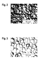
- Example 2 In a manner similar to that of Example 2, an alkaline aqueous solution with its silicon concentration of 3.0 g/L was used as the etching solution. Silicon wafers were etched in a manner similar to that of Example 1. Then, the etching speed, wafer surface roughness, and wafer surface glossiness of the resultant wafers were measured through the above-described testing method. The results are shown in Table 1. Also, in Fig. 1, the surface roughness of the resultant wafers is plotted with respect to the dissolved amount of silicon. Furthermore, a microphotograph of the surface of a resultant wafer was shot and shown in Fig. 3.
- Example 2 An alkaline aqueous solution was formulated in a manner similar to Example 1 except that sodium nitrate was not added, and used as the etching solution. Furthermore, silicon wafers were etched in a manner similar to that of Example 1. Then, the etching speed, wafer surface roughness, and wafer surface glossiness of the resultant wafers were measured through the above-described testing method. The results are shown in Table 1. Also, in Fig. 1, the surface roughness of the resultant wafers is plotted with respect to the dissolved amount of silicon. Furthermore, a microphotograph of the surface of a resultant wafer was shot and shown in Fig. 4.
- Example 2 Etching similar to that of Example 1 was repeatedly performed without replacing the etching solution after the process of Example 12, thereby using an alkaline aqueous solution with the dissolved amount of silicon of 0.3 g/L as the etching solution. Silicon wafers were etched in a manner similar to that of Example 1. Then, the etching speed, wafer surface roughness, and wafer surface glossiness of the resultant wafers were measured through the above-described testing method. The results are shown in Table 1. Also, in Fig. 1, the surface roughness of the resultant wafers is plotted with respect to the dissolved amount of silicon.
- Example 13 In a manner similar to that of Example 13, an alkaline aqueous solution with its silicon concentration of 0.6 g/L was used as the etching solution. Silicon wafers were etched in a manner similar to that of Example 1. Then, the etching speed, wafer surface roughness, and wafer surface glossiness of the resultant wafers were measured through the above-described testing method. The results are shown in Table 1. Also, in Fig. 1, the surface roughness of the resultant wafers is plotted with respect to the dissolved amount of silicon.
- Example 13 In a manner similar to that of Example 13, an alkaline aqueous solution with its silicon concentration of 0.9 g/L was used as the etching solution. Silicon wafers were etched in a manner similar to that of Example 1. Then, the etching speed, wafer surface roughness, and wafer surface glossiness of the resultant wafers were measured through the above-described testing method. The results are shown in Table 1. Also, in Fig. 1, the surface roughness of the resultant wafers is plotted with respect to the dissolved amount of silicon.
- Example 13 In a manner similar to that of Example 13, an alkaline aqueous solution with its silicon concentration of 1.2 g/L was used as the etching solution. Silicon wafers were etched in a manner similar to that of Example 1. Then, the etching speed, wafer surface roughness, and wafer surface glossiness of the resultant wafers were measured through the above-described testing method. The results are shown in Table 1. Also, in Fig. 1, the surface roughness of the resultant wafers is plotted with respect to the dissolved amount of silicon.
- Example 13 In a manner similar to that of Example 13, an alkaline aqueous solution with its silicon concentration of 1.5 g/L was used as the etching solution. Silicon wafers were etched in a manner similar to that of Example 1. Then, the etching speed, wafer surface roughness, and wafer surface glossiness of the resultant wafers were measured through the above-described testing method. The results are shown in Table 1. Also, in Fig. 1, the surface roughness of the resultant wafers is plotted with respect to the dissolved amount of silicon.
- Example 13 In a manner similar to that of Example 13, an alkaline aqueous solution with its silicon concentration of 1.8 g/L was used as the etching solution. Silicon wafers were etched in a manner similar to that of Example 1. Then, the etching speed, wafer surface roughness, and wafer surface glossiness of the resultant wafers were measured through the above-described testing method. The results are shown in Table 1. Also, in Fig. 1, the surface roughness of the resultant wafers is plotted with respect to the dissolved amount of silicon.
- Example 13 In a manner similar to that of Example 13, an alkaline aqueous solution with the dissolved amount of silicon of 2.1 g/L was used as the etching solution. Silicon wafers were etched in a manner similar to that of Example 1. Then, the etching speed, wafer surface roughness, and wafer surface glossiness of the resultant wafers were measured through the above-described testing method. The results are shown in Table 1. Also, in Fig. 1, the surface roughness of the resultant wafers is plotted with respect to the dissolved amount of silicon.
- Example 13 In a manner similar to that of Example 13, an alkaline aqueous solution with its silicon concentration of 2.4 g/L was used as the etching solution. Silicon wafers were etched in a manner similar to that of Example 1. Then, the etching speed, wafer surface roughness, and wafer surface glossiness of the resultant wafers were measured through the above-described testing method. The results are shown in Table 1. Also, in Fig. 1, the surface roughness of the resultant wafers is plotted with respect to the dissolved amount of silicon.
- Example 13 In a manner similar to that of Example 13, an alkaline aqueous solution with its silicon concentration of 2.7 g/L was used as the etching solution. Silicon wafers were etched in a manner similar to that of Example 1. Then, the etching speed, wafer surface roughness, and wafer surface glossiness of the resultant wafers were measured through the above-described testing method. The results are shown in Table 1. Also, in Fig. 1, the surface roughness of the resultant wafers is plotted with respect to the dissolved amount of silicon.
- Example 13 In a manner similar to that of Example 13, an alkaline aqueous solution with its silicon concentration of 3.0 g/L was used as the etching solution. Silicon wafers were etched in a manner similar to that of Example 1. Then, the etching speed, wafer surface roughness, and wafer surface glossiness of the resultant wafers were measured through the above-described testing method. The results are shown in Table 1. Also, in Fig. 1, the surface roughness of the resultant wafers is plotted with respect to the dissolved amount of silicon. Furthermore, microphotograph of the surface of a resultant wafer was shot and shown in Fig. 5.
- alkaline aqueous solution was formulated in a manner similar to Example 1 except that neither sodium bromate nor sodium nitrate was added, and used as the etching solution.
- alkaline aqueous solutions each with the dissolved amount of silicon (g/L) being 0, 0.3, 0.6, 0.9, 1.2, 1.5, 1.8, 2.1, 2.4, 2.7, 3.0 were used as the etching solutions to etch silicon wafers in a manner similar to that of Example 1.
- the etching speed, wafer surface roughness, and wafer surface glossiness of the resultant wafers were measured through the above-described testing method. The results are shown in Table 1. Also, in Fig.
- the surface roughness of the resultant wafers is plotted with respect to the dissolved amount of silicon. Also, in Fig. 1, the surface roughness of the resultant wafers is plotted with respect to the dissolved amount of silicon. Furthermore, microphotographs of the surfaces of the resultant wafers obtained by using the etching solutions with silicon amounts of dissolution of 0 g/L and 3.0 g/L were shot and shown in Figs. 6 and 7, respectively.
- Example 1 0 0.059 0.25 91.7
- Example 2 0.3 0.060 0.25 80.5
- Example 3 0.6 0.058 0.24 89.1
- Example 4 0.9 0.060 0.24 88.8
- Example 5 1.2 0.058 0.25 85.7
- Example 6 1.5 0.059 0.26 87.6
- Example 7 1.8 0.060 0.23 90.5
- Example 8 2.1 0.059 0.25 91.1
- Example 9 2.4 0.059 0.23 86.7
- Example 10 2.7 0.060 0.25 88.8
- Example 11 3.0 0.059 0.25 97.7
- Example 12 0 0.059 0.26 89.9
- Example 13 0.3 0.059 0.24 89.7
- Example 14 0.6 0.061 0.29 110.2 Comparative Example 1 0.9 0.063 0.34 111.1 Comparative Example 2 1.2 0.064 0.32 118.6 Comparative Example 3 1.5 0.064 0.34 119.3 Comparative Example 4
- the size of a facet can be significantly reduced by using the alkaline etching solution according to the present invention.
Landscapes
- Engineering & Computer Science (AREA)
- Chemical & Material Sciences (AREA)
- Manufacturing & Machinery (AREA)
- General Physics & Mathematics (AREA)
- Physics & Mathematics (AREA)
- Computer Hardware Design (AREA)
- Microelectronics & Electronic Packaging (AREA)
- Power Engineering (AREA)
- Condensed Matter Physics & Semiconductors (AREA)
- General Chemical & Material Sciences (AREA)
- Organic Chemistry (AREA)
- Chemical Kinetics & Catalysis (AREA)
- Inorganic Chemistry (AREA)
- Weting (AREA)
- ing And Chemical Polishing (AREA)
- Crystals, And After-Treatments Of Crystals (AREA)
Abstract
Description
- The present invention relates to a field of semiconductor-wafer manufacturing technology and, in particular, to a novel alkaline etching solution for silicon wafer, an alkaline etching method using the solution, a silicon-wafer manufacturing method using the solution, and further a silicon wafer obtained through the method.
- When manufacturing a silicon wafer for use in integrated circuits, such as ICs and LSIs, and discrete semiconductor elements, such as transistors and diodes, a monocrystal obtained through a Czochralski method (CZ method) or a floating-zone method (FZ method) is cut off by using an inner-diameter-blade cutter or a wire saw. After beveling of the edge of the wafer and after a lap process (lapping) is performed for improving the flatness on a main surface with free abrasive grains, wet etching is performed for removing a process distortion applied to the wafer through the above-mentioned processes and then mirror polishing is performed. Such wet etching includes acid etching using a mixed acid of, for example, hydrofluoric acid, nitric acid, and acetic acid, and alkaline etching using alkali, such as sodium hydroxide or potassium hydroxide.
- While acid etching has an advantage being capable of controlling an etching rate and the state of the surface of the wafer after etching, there are drawbacks of a large etching rate to cause deterioration in flatness of the wafer improved through a lapping process.
- On the other hand, although the etching rate is slow, alkaline etching has an advantage of being capable of keeping the flatness of the wafer improved through a lapping process, thereby achieving a wafer with an excellent flatness after etching. In recent years, to allow finer microfabrication, an extremely high-level flatness has been demanded for semiconductor wafers. For this reason, this alkaline etching has been widely used.
- In the alkaline etching technology that has been used so far, an alkaline component with a concentration smaller than 48 to 50 weight percent in an alkaline etching solution has widely been used.
- However, such an alkaline etching solution widely used in general has anisotropy in which an etching speed on a (100) surface and an etching speed on a (111) surface are different from each other by approximately sixty to one hundred times. This poses a problem in which a concave portion (hereinafter referred to as a "facet") occurs on the surface of the wafer, and asperities remain on the surface of the wafer after etching. If such asperities on the surface of the wafer are large (if the surface roughness is large), this poses problems of the occurrence of particles in the device manufacturing process and a decrease in productivity in a polishing process.
- To address such problems, a technology disclosed in, for example,
Japanese Patent Laid-Open Publication No. 2003-229392 - Then, there has been strong demand for the alkaline etching solution for silicon wafers which is capable of improving the surface roughness of wafers without using the alkaline solution with high concentration.
- An object of the present invention is to provide an alkaline etching solution capable of improving a surface roughness even with a relatively low alkaline concentration that has been conventionally widely used, an alkaline etching method using the solution, a silicon-wafer manufacturing method using the solution, and further a silicon wafer obtained through the method with its surface roughness being improved.
- The inventors have diligently studied in order to develop an excellent alkaline etching solution that satisfies the demands described above and, as a result, have found that, by using a bromate-added alkaline etching solution as an alkaline aqueous solution generally used, the size of a facet occurring on the surface of a silicon wafer can be reduced, thereby completing the present invention.
- Also, the inventors have found that effects of bromate obtained from the findings in alkaline etching can be kept by adding nitrate, thereby completing the present invention.
- That is, the present invention relates to an alkaline etching solution in which an alkaline aqueous solution contains bromate.
- Further, the present invention relates to an alkaline etching solution in which an alkaline aqueous solution contains bromate and nitrate.
- Still further, the present invention relates to the alkaline etching solution, wherein the bromate is sodium bromate.
- Still further, the present invention relates to the alkaline etching solution, wherein the nitrate is sodium nitrate.
- Still further, the present invention relates to a method of etching a silicon wafer with an alkaline solution, wherein the alkaline solution is an alkaline aqueous solution containing bromate.
- Still further, the present invention relates to a method of etching a silicon wafer with an alkaline solution, wherein the alkaline solution is an alkaline aqueous solution containing bromate and nitrate.
- Still further, the present invention relates to the silicon-wafer etching method, wherein the bromate is sodium bromate.
- Still further, the present invention relates to the silicon-wafer etching method, wherein the nitrate is sodium nitrate.
- Still further, the present invention relates to a method of manufacturing a semiconductor silicon wafer, comprising the step of performing alkaline etching by using an alkaline aqueous solution containing bromate, wherein a wafer after the etching has a surface roughness Ra equal to or smaller than 0.27 µm.
- By using the alkaline etching solution containing bromate, the size of the facet can be significantly reduced and the surface roughness of the wafer can be improved without significant decrease in etching speed, compared with the case of using an alkaline aqueous solution conventionally used in general. Also, the surface roughness can be sufficiently improved without a high-concentration alkaline aqueous solution. Therefore, alkaline etching can be conveniently performed. Furthermore, by using an alkaline etching solution containing bromate and nitrate, bromate consumption is suppressed in the course of alkaline etching, thereby keeping the above-described effects. Thus, it is possible to perform alkaline etching capable of obtaining a wafer with improved surface roughness in an extremely economical manner with a low environmental load.
- Best embodiment for carrying out the invention
- A silicon wafer capable of being etched by applying the etching solution of the present invention is not particularly restrictive. The etching solution of the present invention can be applied to various silicon wafers conventionally known to the art. Specifically, there are no limitations in size (diameter and thickness), the presence or absence of doping with various elements, or the presence or absence of pre-process.
- The alkaline etching solution according to the present invention has a feature in which a conventionally-known alkaline etching solution for silicon wafer contains a small amount of bromate. Here, the alkaline etching solution means an aqueous solution containing an alkaline component as an etching component and, if required, other components.
- Here, the alkaline etching solution usable in the present invention is not particularly restrictive as long as it is a conventionally-known alkaline etching solution for silicon wafer including ones commercially available. The alkaline etching solution can be selected appropriately in view of a desired etching characteristic and characteristics of a semiconductor wafer to be etched. As an alkaline component, an inorganic alkali hydroxide is preferable. In particular, sodium hydroxide, potassium hydroxide, and lithium hydroxide, and a mixture thereof are preferable. In the present invention, the use of sodium hydroxide is particularly preferable.
- Also, the concentration of the alkaline component is not particularly restrictive and can be selected appropriately according to etching conditions and others. A general range of concentration of the alkaline component is 20 to 60 weight percent and, preferably, 45 to 50 weight percent. Here, the concentration of the alkaline component represents a weight percent of alkaline hydroxide in the aqueous solution. If the concentration is lower than the above range, it is difficult to control the etching speed and suppress a facet on the surface. A concentration higher than the above range is not preferable because of posing problems such as insolubility of bromate in a high-concentration alkaline aqueous solution and freeze of the alkaline aqueous solution itself.
- Furthermore, the purity of the alkaline component usable in the present invention is not particularly restrictive and can be selected appropriately in consideration of the degree of metallic contamination associated with etching. When using in a semiconductor manufacturing process, a commercially-available solution with high purity can be used as it is. Also, if required, the solution is preferably formulated from an alkaline component with a low concentration of metallic impurities contained therein and ultrapure water.
- Still further, since the concentration of the alkaline component varies according to the etching, it is preferable to measure the concentration appropriately at the time of use or the like, and re-supply an etching solution or water as required. A measurement can be performed by using, for example, neutralization titration. Still further, although normal storage conditions will suffice, an environment that can prevent the occurrence of alkaline carbonate, which will cause a change in concentration and affect etching, is preferable.
- The alkaline etching solution according to the present invention has a feature of containing bromate. Here, the bromate is not particularly restrictive, and can include sodium bromate, potassium bromate, and lithium bromate. In particular, sodium salt is preferable. As the bromate, the one commercially available can be used as it is or after purification.
- The concentration of the bromate is not particularly restrictive. A preferable range is 0.01 to 10 weight percent, more preferably, 0.1 to 3.0 weight percent, and still more preferably, 0.1 to 1.0 weight percent. If the concentration is too low, a sufficient improvement in surface roughness cannot be obtained. Also, a concentration higher than the above range is not preferable in view of cost and possible mixture of impurities from the bromate.
- A method of adding the bromate is not particularly restrictive. The bromate can be solved in advance before use for storage and can be used as it is for etching. Alternatively, the solution can be formulated at the time of use for etching. On the other hand, the inventors have found that, when a bromate-containing alkaline etching solution is used for etching, as the number of times of etching is increased, the effect of addition of the bromate is decreased. Since the alkaline etching solution may be used under different etching conditions or used for etching of silicon wafers of various shapes, it is preferable to calculate the dissolved amount of silicon in the etching solution that can be found from the amount of etching, in place of the number of times of etching. Therefore, if the dissolved amount of silicon is increased and the effect is decreased, the etching solution may be replaced, or bromate may be further added for use.
- Another preferable feature of the alkaline etching solution according to the present invention is that nitrate is added in addition to bromate. Effects of the nitrate are based on unexpected findings described below obtained by the inventors. That is, in an alkaline etching method using a bromate-added alkaline aqueous solution, the facet size is indeed excellently controlled and can be extremely decreased, thereby obtaining a silicon wafer with an improved surface roughness. However, if such an alkaline etching solution is repeatedly used, the above effects are decreased. However, when the alkaline etching solution with nitrate further added thereto is used, the above effects can be kept without reduction.
- The nitrate to be added for this purpose is not particularly restrictive, and can include sodium nitrate, potassium nitrate, and lithium nitrate with high purity. In the present invention, sodium nitrate is preferable. As the nitrate, the one commercially available can be used as it is or after purification.
- The concentration of the nitrate is not particularly restrictive. A preferable range for use to achieve the effects is 0.01 to 10.0 weight percent. In particular, the nitrate is preferably equimolecular to or more than the bromate. By adding the nitrate equimolecular to or more than the bromate being added, the above effects can be kept for the longer time even when the alkaline etching solution is used repeatedly.
- A method of adding the nitrate is not particularly restrictive. The nitrate can be added to the alkaline aqueous solution irrespectively of the order of addition of the bromate. Also, the nitrate can be solved in advance before use for storage and can be used as it is for etching. Alternatively, the solution can be formulated at the time of use for etching.
- The alkaline etching method according to the present invention has a feature of using any of the above alkaline etching solutions and, in particular, the method is for (semiconductor) silicon wafer.
- Etching conditions for use in the alkaline etching method according to the present invention are not particularly restrictive.
- Conditions that are set when a conventionally-known alkaline etching solution is used are preferable and, according to the type of a semiconductor wafer to be etched (size, thickness, crystal orientation), any etching amount, etching speed, etching time, temperature, agitation, and others can be selected appropriately.
- Furthermore, an etching apparatus usable for the alkaline etching method according to the present invention is not particularly restrictive. An apparatus used when a conventionally-known alkaline etching solution is used is preferable and, according to the type of a semiconductor wafer to be etched and the etching conditions, any apparatus can be selected appropriately. Specifically, for example, an etching bath having a circulating system, such as a circulating pump, a filter, and a heater, is usable.
- The etching method using the alkaline etching solution containing bromate according to the present invention is excellent in that a silicon wafer with an improved surface roughness can be obtained. On the other hand, only with bromate, the effects are decreasing as etching is repeated. Therefore, the degree of repeated use is preferably determined by performing etching using an appropriate standard test sample and measuring surface roughness of a silicon wafer obtained with respect to the dissolved amount of silicon in the etching solution for comparison.
- Also, the etching method using the alkaline etching solution containing bromate and nitrate suppresses a decrease in the effects of the bromate in accordance with repetition of etching, and therefore can be used repeatedly. Also in this case, the degree of such repeated use is preferably determined by performing etching using an appropriate standard test sample and measuring surface roughness of a silicon wafer obtained with respect to the dissolved amount of silicon in the etching solution for comparison.
- Semiconductor-silicon-wafer manufacturing method The semiconductor-silicon-wafer manufacturing method according to the present invention has a feature of performing alkaline etching by using the alkaline etching solution according to the present invention to manufacture a semiconductor silicon wafer.
- The semiconductor silicon wafer manufactured through the manufacturing method according to the present invention is particularly excellent in surface roughness. The surface roughness can be evaluated through various measuring schemes according to various purposes. In particular, such an evaluation can be made from the surface roughness and/or surface glossiness measured through various measuring means conventionally known. Specific measuring apparatuses and methods include Surftest SJ-201P from Mitsutoyo Corporation for surface roughness and a glossmeter PG-1M from Nippon Denshoku Industries, Co., Ltd., for surface glossiness.
- Furthermore, the purpose of visually evaluating the shape of facet can be fulfilled by observing the shape of the surface. Specifically, a surface observation by a microscope is a preferable evaluation method. With this, for example, the shape, size, and depth of the facet can be evaluated.
- The present invention is described in more detail below with reference to the examples, but is not restricted to these examples.
- In examples and comparative examples described below, the following evaluation method was used.
-
- (1) Etching speed (etching rate: µm/sec) : Ultragate 9700 from ADE was used to measure the thickness of the center of a wafer before and after etching, and an etching speed was calculated based on the following equation:
- Etching speed: (Thickness before etching-Thickness after etching)/etching time.
- (2) Wafer surface roughness: Surftest SJ-201P from Mitsutoyo Corporation was used to measure Ra based on JIS B0601-1994.
- (3) Wafer surface glossiness: A glossmeter PG-1M from Nippon Denshoku Industries, Co., Ltd. was used to measure the glossiness based on JIS Z8741/K5400 with a lighting/light-receiving angle of 60 degrees.
- (4) Etching surface observation: A surface-shape measurement microscope VF-7500 from Keyence Corporation was used for wafer surface observation after etching (magnification: 100×).
- In an alkaline aqueous solution of 65 L of 48 weight percent of sodium hydroxide (48% of CLEARCUT-S from Tsurumi Soda Co., Ltd.), 196 g of sodium bromate (from Wako Pure Chemical Industries, Ltd., a Wako reagent chemicals) and 111 g of sodium nitrate (from Wako Pure Chemical Industries, Ltd., reagent chemicals) were dissolved to formulate an alkaline aqueous solution containing 0.20 weight percent of sodium bromate and 0.11 weight percent of sodium nitrate as an alkaline etching solution. With the formulated alkaline etching solution, a block-type etching bath with a filling capacity of 65 liters was filled. In the filling bath, twenty silicon wafers having a diameter of eight inches subjected to both-side lapping were soaked as being loaded on a carrier. With these wafers being rotated in the aqueous solution together with the carrier (20 rpm), etching was performed for approximately 25 µm on both sides for approximately seven minutes at a liquid temperature of 90 degrees Celsius. Then, the wafers were moved to a water washing bath for cleaning and drying. Then, the etching speed, wafer surface roughness, and wafer surface glossiness of the resultant wafers were measured through the above-described testing method. The results are shown in Table 1. Also, in Fig. 1, the surface roughness of the resultant wafers is plotted with respect to the dissolved amount of silicon. Furthermore, a microphotograph of the surface of a resultant wafer was shot and shown in Fig. 2.
- Etching similar to that of Example 1 was repeatedly performed without replacing the etching solution after the process of Example 1, thereby using an alkaline aqueous solution with the dissolved amount of silicon of 0.3 g/L as the etching solution. Silicon wafers were etched in a manner similar to that of Example 1. Then, the etching speed, wafer surface roughness, and wafer surface glossiness of the resultant wafers were measured through the above-described testing method. The results are shown in Table 1. Also, in Fig. 1, the surface roughness of the resultant wafers is plotted with respect to the dissolved amount of silicon.
- In a manner similar to that of Example 2, an alkaline aqueous solution with its silicon concentration of 0.6 g/L was used as the etching solution. Silicon wafers were etched in a manner similar to that of Example 1. Then, the etching speed, wafer surface roughness, and wafer surface glossiness of the resultant wafers were measured through the above-described testing method. The results are shown in Table 1. Also, in Fig. 1, the surface roughness of the resultant wafers is plotted with respect to the dissolved amount of silicon.
- In a manner similar to that of Example 2, an alkaline aqueous solution with its silicon concentration of 0.9 g/L was used as the etching solution. Silicon wafers were etched in a manner similar to that of Example 1. Then, the etching speed, wafer surface roughness, and wafer surface glossiness of the resultant wafers were measured through the above-described testing method. The results are shown in Table 1. Also, in Fig. 1, the surface roughness of the resultant wafers is plotted with respect to the dissolved amount of silicon.
- In a manner similar to that of Example 2, an alkaline aqueous solution with its silicon concentration of 1.2 g/L was used as the etching solution. Silicon wafers were etched in a manner similar to that of Example 1. Then, the etching speed, wafer surface roughness, and wafer surface glossiness of the resultant wafers were measured through the above-described testing method. The results are shown in Table 1. Also, in Fig. 1, the surface roughness of the resultant wafers is plotted with respect to the dissolved amount of silicon.
- In a manner similar to that of Example 2, an alkaline aqueous solution with its silicon concentration of 1.5 g/L was used as the etching solution. Silicon wafers were etched in a manner similar to that of Example 1. Then, the etching speed, wafer surface roughness, and wafer surface glossiness of the resultant wafers were measured through the above-described testing method. The results are shown in Table 1. Also, in Fig. 1, the surface roughness of the resultant wafers is plotted with respect to the dissolved amount of silicon.
- In a manner similar to that of Example 2, an alkaline aqueous solution with its silicon concentration of 1.8 g/L was used as the etching solution. Silicon wafers were etched in a manner similar to that of Example 1. Then, the etching speed, wafer surface roughness, and wafer surface glossiness of the resultant wafers were measured through the above-described testing method. The results are shown in Table 1. Also, in Fig. 1, the surface roughness of the resultant wafers is plotted with respect to the dissolved amount of silicon.
- In a manner similar to that of Example 2, an alkaline aqueous solution with its silicon concentration of 2.1 g/L was used as the etching solution. Silicon wafers were etched in a manner similar to that of Example 1. Then, the etching speed, wafer surface roughness, and wafer surface glossiness of the resultant wafers were measured through the above-described testing method. The results are shown in Table 1. Also, in Fig. 1, the surface roughness of the resultant wafers is plotted with respect to the dissolved amount of silicon.
- In a manner similar to that of Example 2, an alkaline aqueous solution with its silicon concentration of 2.4 g/L was used as the etching solution. Silicon wafers were etched in a manner similar to that of Example 1. Then, the etching speed, wafer surface roughness, and wafer surface glossiness of the resultant wafers were measured through the above-described testing method. The results are shown in Table 1. Also, in Fig. 1, the surface roughness of the resultant wafers is plotted with respect to the dissolved amount of silicon.
- In a manner similar to that of Example 2, an alkaline aqueous solution with its silicon concentration of 2.7 g/L was used as the etching solution. Silicon wafers were etched in a manner similar to that of Example 1. Then, the etching speed, wafer surface roughness, and wafer surface glossiness of the resultant wafers were measured through the above-described testing method. The results are shown in Table 1. Also, in Fig. 1, the surface roughness of the resultant wafers is plotted with respect to the dissolved amount of silicon.
- In a manner similar to that of Example 2, an alkaline aqueous solution with its silicon concentration of 3.0 g/L was used as the etching solution. Silicon wafers were etched in a manner similar to that of Example 1. Then, the etching speed, wafer surface roughness, and wafer surface glossiness of the resultant wafers were measured through the above-described testing method. The results are shown in Table 1. Also, in Fig. 1, the surface roughness of the resultant wafers is plotted with respect to the dissolved amount of silicon. Furthermore, a microphotograph of the surface of a resultant wafer was shot and shown in Fig. 3.
- An alkaline aqueous solution was formulated in a manner similar to Example 1 except that sodium nitrate was not added, and used as the etching solution. Furthermore, silicon wafers were etched in a manner similar to that of Example 1. Then, the etching speed, wafer surface roughness, and wafer surface glossiness of the resultant wafers were measured through the above-described testing method. The results are shown in Table 1. Also, in Fig. 1, the surface roughness of the resultant wafers is plotted with respect to the dissolved amount of silicon. Furthermore, a microphotograph of the surface of a resultant wafer was shot and shown in Fig. 4.
- Etching similar to that of Example 1 was repeatedly performed without replacing the etching solution after the process of Example 12, thereby using an alkaline aqueous solution with the dissolved amount of silicon of 0.3 g/L as the etching solution. Silicon wafers were etched in a manner similar to that of Example 1. Then, the etching speed, wafer surface roughness, and wafer surface glossiness of the resultant wafers were measured through the above-described testing method. The results are shown in Table 1. Also, in Fig. 1, the surface roughness of the resultant wafers is plotted with respect to the dissolved amount of silicon.
- In a manner similar to that of Example 13, an alkaline aqueous solution with its silicon concentration of 0.6 g/L was used as the etching solution. Silicon wafers were etched in a manner similar to that of Example 1. Then, the etching speed, wafer surface roughness, and wafer surface glossiness of the resultant wafers were measured through the above-described testing method. The results are shown in Table 1. Also, in Fig. 1, the surface roughness of the resultant wafers is plotted with respect to the dissolved amount of silicon.
- In a manner similar to that of Example 13, an alkaline aqueous solution with its silicon concentration of 0.9 g/L was used as the etching solution. Silicon wafers were etched in a manner similar to that of Example 1. Then, the etching speed, wafer surface roughness, and wafer surface glossiness of the resultant wafers were measured through the above-described testing method. The results are shown in Table 1. Also, in Fig. 1, the surface roughness of the resultant wafers is plotted with respect to the dissolved amount of silicon.
- In a manner similar to that of Example 13, an alkaline aqueous solution with its silicon concentration of 1.2 g/L was used as the etching solution. Silicon wafers were etched in a manner similar to that of Example 1. Then, the etching speed, wafer surface roughness, and wafer surface glossiness of the resultant wafers were measured through the above-described testing method. The results are shown in Table 1. Also, in Fig. 1, the surface roughness of the resultant wafers is plotted with respect to the dissolved amount of silicon.
- In a manner similar to that of Example 13, an alkaline aqueous solution with its silicon concentration of 1.5 g/L was used as the etching solution. Silicon wafers were etched in a manner similar to that of Example 1. Then, the etching speed, wafer surface roughness, and wafer surface glossiness of the resultant wafers were measured through the above-described testing method. The results are shown in Table 1. Also, in Fig. 1, the surface roughness of the resultant wafers is plotted with respect to the dissolved amount of silicon.
- In a manner similar to that of Example 13, an alkaline aqueous solution with its silicon concentration of 1.8 g/L was used as the etching solution. Silicon wafers were etched in a manner similar to that of Example 1. Then, the etching speed, wafer surface roughness, and wafer surface glossiness of the resultant wafers were measured through the above-described testing method. The results are shown in Table 1. Also, in Fig. 1, the surface roughness of the resultant wafers is plotted with respect to the dissolved amount of silicon.
- In a manner similar to that of Example 13, an alkaline aqueous solution with the dissolved amount of silicon of 2.1 g/L was used as the etching solution. Silicon wafers were etched in a manner similar to that of Example 1. Then, the etching speed, wafer surface roughness, and wafer surface glossiness of the resultant wafers were measured through the above-described testing method. The results are shown in Table 1. Also, in Fig. 1, the surface roughness of the resultant wafers is plotted with respect to the dissolved amount of silicon.
- In a manner similar to that of Example 13, an alkaline aqueous solution with its silicon concentration of 2.4 g/L was used as the etching solution. Silicon wafers were etched in a manner similar to that of Example 1. Then, the etching speed, wafer surface roughness, and wafer surface glossiness of the resultant wafers were measured through the above-described testing method. The results are shown in Table 1. Also, in Fig. 1, the surface roughness of the resultant wafers is plotted with respect to the dissolved amount of silicon.
- In a manner similar to that of Example 13, an alkaline aqueous solution with its silicon concentration of 2.7 g/L was used as the etching solution. Silicon wafers were etched in a manner similar to that of Example 1. Then, the etching speed, wafer surface roughness, and wafer surface glossiness of the resultant wafers were measured through the above-described testing method. The results are shown in Table 1. Also, in Fig. 1, the surface roughness of the resultant wafers is plotted with respect to the dissolved amount of silicon.
- In a manner similar to that of Example 13, an alkaline aqueous solution with its silicon concentration of 3.0 g/L was used as the etching solution. Silicon wafers were etched in a manner similar to that of Example 1. Then, the etching speed, wafer surface roughness, and wafer surface glossiness of the resultant wafers were measured through the above-described testing method. The results are shown in Table 1. Also, in Fig. 1, the surface roughness of the resultant wafers is plotted with respect to the dissolved amount of silicon. Furthermore, microphotograph of the surface of a resultant wafer was shot and shown in Fig. 5.
- An alkaline aqueous solution was formulated in a manner similar to Example 1 except that neither sodium bromate nor sodium nitrate was added, and used as the etching solution. In a manner similar to those of Examples 1 to 11, alkaline aqueous solutions each with the dissolved amount of silicon (g/L) being 0, 0.3, 0.6, 0.9, 1.2, 1.5, 1.8, 2.1, 2.4, 2.7, 3.0 were used as the etching solutions to etch silicon wafers in a manner similar to that of Example 1. Then, the etching speed, wafer surface roughness, and wafer surface glossiness of the resultant wafers were measured through the above-described testing method. The results are shown in Table 1. Also, in Fig. 1, the surface roughness of the resultant wafers is plotted with respect to the dissolved amount of silicon. Also, in Fig. 1, the surface roughness of the resultant wafers is plotted with respect to the dissolved amount of silicon. Furthermore, microphotographs of the surfaces of the resultant wafers obtained by using the etching solutions with silicon amounts of dissolution of 0 g/L and 3.0 g/L were shot and shown in Figs. 6 and 7, respectively.
Table 1 Evaluation Dissolved amount of silicon in etching solution [g/L] Etching speed [µm/sec] Surface roughness Ra [µm] Glossiness Example 1 0 0.059 0.25 91.7 Example 2 0.3 0.060 0.25 80.5 Example 3 0.6 0.058 0.24 89.1 Example 4 0.9 0.060 0.24 88.8 Example 5 1.2 0.058 0.25 85.7 Example 6 1.5 0.059 0.26 87.6 Example 7 1.8 0.060 0.23 90.5 Example 8 2.1 0.059 0.25 91.1 Example 9 2.4 0.059 0.23 86.7 Example 10 2.7 0.060 0.25 88.8 Example 11 3.0 0.059 0.25 97.7 Example 12 0 0.059 0.26 89.9 Example 13 0.3 0.059 0.24 89.7 Example 14 0.6 0.061 0.29 110.2 Comparative Example 1 0.9 0.063 0.34 111.1 Comparative Example 2 1.2 0.064 0.32 118.6 Comparative Example 3 1.5 0.064 0.34 119.3 Comparative Example 4 1.8 0.062 0.34 119.2 Comparative Example 5 2.1 0.064 0.33 118.4 Comparative Example 6 2.4 0.063 0.33 118.9 Comparative Example 7 2.7 0.064 0.34 121.1 Comparative Example 8 3.0 0.064 0.36 117.4 Comparative Example 9 0 0.062 0.34 120.5 0.3 0.064 0.32 121.5 0.6 0.063 0.33 120.3 0.9 0.065 0.33 119.7 1.2 0.064 0.35 122.1 1.5 0.063 0.31 122.6 1.8 0.063 0.33 123.9 2.1 0.064 0.32 123.6 2.4 0.064 0.32 124.5 2.7 0.062 0.34 124.1 3.0 0.064 0.32 123.8 - Also, in comparison with Figs. 2 to 4 and Figs. 5 to 7, the size of a facet can be significantly reduced by using the alkaline etching solution according to the present invention.
-
- Fig. 1 shows a graph depicting the results of Examples 1 to 14 and Comparative Examples 1 to 9. The horizontal axis represents dissolved amount of silicon (g/L) and the vertical axis represents a surface roughness (µm) of a wafer obtained. The hollow circles represent alkaline etching solution containing sodium bromate and sodium nitrate (Examples 1 to 11), the crosses represent alkaline etching solution containing sodium bromate (Examples 12 to 14 and Comparative Examples 1 to 8), and black circles represent alkaline etching solution of 48% NaOH (Comparative Example 9);
- Fig. 2 shows a micrograph (magnification: 100x) of a wafer surface obtained through Example 1;
- Fig. 3 shows a micrograph (magnification: 100x) of a wafer surface obtained through Example 11;
- Fig. 4 shows a micrograph (magnification: 100x) of a wafer surface obtained through Example 12;
- Fig. 5 shows a micrograph (magnification: 100x) of a wafer surface obtained through Comparative Example 8;
- Fig. 6 shows a micrograph (magnification: 100x) of a wafer surface obtained through Comparative Example 9 (dissolved amount of silicon: 0 g/L); and
- Fig. 7 shows a micrograph (magnification: 100x) of a wafer surface obtained Comparative Example 9 (dissolved amount of silicon: 3.0 g/L).
Claims (13)
- An alkaline aqueous solution comprising bromate.
- The alkaline aqueous solution according to claim 1, wherein the alkaline aqueous solution additionally comprises nitrate.
- The alkaline aqueous solution according to claim 1 or 2, wherein the bromate is sodium bromate.
- The alkaline aqueous solution according to claim 2 or 3, wherein the nitrate is sodium nitrate.
- A silicon-wafer etching method using an alkaline solution, wherein the alkaline solution is an alkaline aqueous solution comprising bromate.
- The silicon-wafer etching method according to claim 5, wherein the alkaline solution additionally comprises nitrate.
- The silicon-wafer etching method according to claim 5 or 6, wherein the alkaline solution comprises an alkali hydroxide in a concentration of 20 - 60 % by weight.
- The silicon-wafer etching method according to claim 7, wherein the alkaline solution comprises an alkali hydroxide in a concentration of 45 - 50 % by weight.
- The silicon-wafer etching method according to any one of claims 5 to 8, wherein the bromate is sodium bromate.
- The silicon-wafer etching method according to any one of claims 6 to 9, wherein the nitrate is sodium nitrate.
- The silicon-wafer etching method according to any one of claims 5 - 10, wherein a wafer after the etching has a surface roughness Ra equal to or smaller than 0.27 µm.
- The silicon-wafer etching method according to any one of claims 5 to 11, wherein the concentration of the bromate is 0.01 to 10 % by weight.
- The silicon-wafer etching method according to any one of claims 6 to 12, wherein the concentration of the nitrate is 0.01 to 10 % by weight.
Applications Claiming Priority (1)
| Application Number | Priority Date | Filing Date | Title |
|---|---|---|---|
| JP2006243350A JP5017709B2 (en) | 2006-09-07 | 2006-09-07 | Silicon wafer etching method and semiconductor silicon wafer manufacturing method |
Publications (3)
| Publication Number | Publication Date |
|---|---|
| EP1898454A2 true EP1898454A2 (en) | 2008-03-12 |
| EP1898454A3 EP1898454A3 (en) | 2008-06-04 |
| EP1898454B1 EP1898454B1 (en) | 2010-01-06 |
Family
ID=38819860
Family Applications (1)
| Application Number | Title | Priority Date | Filing Date |
|---|---|---|---|
| EP07016454A Active EP1898454B1 (en) | 2006-09-07 | 2007-08-22 | Alkaline etching method for a semiconductor wafer |
Country Status (8)
| Country | Link |
|---|---|
| US (1) | US7780868B2 (en) |
| EP (1) | EP1898454B1 (en) |
| JP (1) | JP5017709B2 (en) |
| KR (1) | KR100983064B1 (en) |
| CN (1) | CN101158052B (en) |
| DE (1) | DE602007004154D1 (en) |
| SG (1) | SG140530A1 (en) |
| TW (1) | TWI354695B (en) |
Families Citing this family (6)
| Publication number | Priority date | Publication date | Assignee | Title |
|---|---|---|---|---|
| US20110020966A1 (en) * | 2009-07-23 | 2011-01-27 | Canon Kabushiki Kaisha | Method for processing silicon substrate and method for producing substrate for liquid ejecting head |
| JP5216749B2 (en) * | 2009-11-02 | 2013-06-19 | ジルトロニック アクチエンゲゼルシャフト | Processing method of silicon wafer |
| CN102154710B (en) * | 2010-12-09 | 2013-09-11 | 扬州瀚源新材料科技有限公司 | Monocrystal silicon wafer flocking process liquid and preparation method thereof |
| CN103603054A (en) * | 2013-10-15 | 2014-02-26 | 电子科技大学 | Method for preparing lithium tantalite wafer |
| CN103773374B (en) * | 2014-01-26 | 2015-03-11 | 内蒙古日月太阳能科技有限责任公司 | Alkaline corrosive liquid and method for corroding polycrystalline silicon chips |
| CN111211049B (en) * | 2018-11-21 | 2022-10-21 | 浙江海晫新能源科技有限公司 | Silicon wafer alkali corrosion process and application thereof |
Citations (2)
| Publication number | Priority date | Publication date | Assignee | Title |
|---|---|---|---|---|
| GB1278499A (en) | 1968-10-17 | 1972-06-21 | Texas Instruments Inc | Improved process for polishing oxidizable surfaces |
| JP2003229392A (en) | 2001-11-28 | 2003-08-15 | Shin Etsu Handotai Co Ltd | Method for manufacturing silicon wafer, silicon wafer and soi wafer |
Family Cites Families (22)
| Publication number | Priority date | Publication date | Assignee | Title |
|---|---|---|---|---|
| US1923618A (en) * | 1932-07-30 | 1933-08-22 | Philip H Groggins | Preparation of amino derivatives of the anthraquinone series |
| FR2374396A1 (en) * | 1976-12-17 | 1978-07-13 | Ibm | SILICON PICKLING COMPOSITION |
| TW332322B (en) | 1994-03-31 | 1998-05-21 | Furontec Kk | Manufacturing method for etchant and electronic element of conductive semiconductor |
| US6168725B1 (en) * | 1997-12-22 | 2001-01-02 | Visteon Global Technologies, Inc. | Etching of Al-Cu layers to form electronic circuits using base solutions including nitrites, borates or bromates |
| JP4306827B2 (en) * | 1998-04-14 | 2009-08-05 | エルジー ディスプレイ カンパニー リミテッド | Etching agent |
| JP4094110B2 (en) * | 1998-04-14 | 2008-06-04 | エルジー.フィリップス エルシーデー カンパニー,リミテッド | Etching agent |
| US6232228B1 (en) | 1998-06-25 | 2001-05-15 | Samsung Electronics Co., Ltd. | Method of manufacturing semiconductor devices, etching composition for manufacturing semiconductor devices, and semiconductor devices made using the method |
| KR100271769B1 (en) | 1998-06-25 | 2001-02-01 | 윤종용 | Method for manufacturing semiconductor device, etchant composition and semiconductor device for manufacturing semiconductor device therefor |
| JP3765970B2 (en) * | 2000-07-12 | 2006-04-12 | ソニーケミカル株式会社 | Etching solution and method for manufacturing flexible wiring board |
| JP2002322578A (en) * | 2001-04-24 | 2002-11-08 | Noritake Co Ltd | Etching solution for aluminum thin film and method for forming aluminum thin pattern |
| US6740253B2 (en) * | 2002-01-23 | 2004-05-25 | Council Of Scientific And Industrial Research | Preparation of non-hazardous brominating reagents |
| US20030139047A1 (en) * | 2002-01-24 | 2003-07-24 | Thomas Terence M. | Metal polishing slurry having a static etch inhibitor and method of formulation |
| JP4010819B2 (en) * | 2002-02-04 | 2007-11-21 | Necエレクトロニクス株式会社 | Manufacturing method of semiconductor device |
| DE10241300A1 (en) * | 2002-09-04 | 2004-03-18 | Merck Patent Gmbh | Etching for silicon surfaces and layers, used in photovoltaic, semiconductor and high power electronics technology, for producing photodiode, circuit, electronic device or solar cell, is thickened alkaline liquid |
| TW200411759A (en) * | 2002-09-18 | 2004-07-01 | Memc Electronic Materials | Process for etching silicon wafers |
| TW200423247A (en) * | 2002-10-25 | 2004-11-01 | Intersurface Dynamics | Method for using additives in the caustic etching of silicon for obtaining improved surface characteristics |
| JP2005175223A (en) * | 2003-12-11 | 2005-06-30 | Fujikura Ltd | Etching method of silicon wafer |
| JP4700333B2 (en) | 2003-12-22 | 2011-06-15 | シルトロニック・ジャパン株式会社 | High purity alkali etching solution for silicon wafer and silicon wafer alkali etching method |
| US20060118760A1 (en) | 2004-12-03 | 2006-06-08 | Yang Andy C | Slurry composition and methods for chemical mechanical polishing |
| JP4792802B2 (en) * | 2005-04-26 | 2011-10-12 | 住友電気工業株式会社 | Surface treatment method of group III nitride crystal |
| EP1918985B1 (en) * | 2006-10-31 | 2010-05-26 | S.O.I.TEC. Silicon on Insulator Technologies S.A. | Methods for characterizing defects on silicon surfaces, etching composition for silicon surfaces and process of treating silicon surfaces with the etching composition |
| EP1923618A3 (en) | 2006-11-15 | 2010-05-26 | Specmat Limited | Apparatus for connecting together two objects and chair incorporating the same |
-
2006
- 2006-09-07 JP JP2006243350A patent/JP5017709B2/en active Active
-
2007
- 2007-07-25 SG SG200705460-4A patent/SG140530A1/en unknown
- 2007-08-17 CN CN2007101416546A patent/CN101158052B/en active Active
- 2007-08-22 EP EP07016454A patent/EP1898454B1/en active Active
- 2007-08-22 TW TW096131025A patent/TWI354695B/en active
- 2007-08-22 DE DE602007004154T patent/DE602007004154D1/en active Active
- 2007-08-27 KR KR1020070086054A patent/KR100983064B1/en active IP Right Grant
- 2007-09-05 US US11/899,182 patent/US7780868B2/en active Active
Patent Citations (2)
| Publication number | Priority date | Publication date | Assignee | Title |
|---|---|---|---|---|
| GB1278499A (en) | 1968-10-17 | 1972-06-21 | Texas Instruments Inc | Improved process for polishing oxidizable surfaces |
| JP2003229392A (en) | 2001-11-28 | 2003-08-15 | Shin Etsu Handotai Co Ltd | Method for manufacturing silicon wafer, silicon wafer and soi wafer |
Also Published As
| Publication number | Publication date |
|---|---|
| US7780868B2 (en) | 2010-08-24 |
| KR100983064B1 (en) | 2010-09-20 |
| SG140530A1 (en) | 2008-03-28 |
| US20080064222A1 (en) | 2008-03-13 |
| JP2008066538A (en) | 2008-03-21 |
| EP1898454A3 (en) | 2008-06-04 |
| DE602007004154D1 (en) | 2010-02-25 |
| CN101158052B (en) | 2010-09-29 |
| TWI354695B (en) | 2011-12-21 |
| EP1898454B1 (en) | 2010-01-06 |
| JP5017709B2 (en) | 2012-09-05 |
| KR20080023119A (en) | 2008-03-12 |
| TW200813194A (en) | 2008-03-16 |
| CN101158052A (en) | 2008-04-09 |
Similar Documents
| Publication | Publication Date | Title |
|---|---|---|
| EP1898454B1 (en) | Alkaline etching method for a semiconductor wafer | |
| TWI292586B (en) | ||
| US20040108297A1 (en) | Process for etching silicon wafers | |
| EP1852480B1 (en) | Method of processing a surface of group III nitride crystal and group III nitride crystal substrate | |
| JP2006222453A (en) | Silicon wafer, method for manufacturing the same, and soi wafer | |
| KR100706683B1 (en) | Silicon wafer processing method | |
| US20090042390A1 (en) | Etchant for silicon wafer surface shape control and method for manufacturing silicon wafers using the same | |
| EP0926714A1 (en) | Silicon wafer storage water and silicon wafer storage method | |
| US7479204B2 (en) | Method of manufacturing semiconductor substrate and method of evaluating quality of semiconductor substrate | |
| EP1533402A1 (en) | Epitaxial wafer and its manufacturing method | |
| EP1548812B1 (en) | High-purity alkali etching solution for silicon wafers and alkali etching method of silicon wafer | |
| US20090203212A1 (en) | Surface Grinding Method and Manufacturing Method for Semiconductor Wafer | |
| JP5216749B2 (en) | Processing method of silicon wafer | |
| CN113906171A (en) | Method for manufacturing single crystal silicon wafer and single crystal silicon wafer | |
| JP2009141165A (en) | Method of etching silicon wafer | |
| JP2006093453A (en) | Alkali etchant and alkali etching method | |
| EP3950877A1 (en) | Method for polishing to-be-polished object including material having silicon-silicon bond | |
| JP3400694B2 (en) | Silicon wafer etching method | |
| KR20220042842A (en) | Method for wet texturing of solar cell substrate | |
| JP4784287B2 (en) | Crystal defect evaluation method of silicon single crystal substrate | |
| JP2004063954A (en) | Etching method of silicon wafer, and method of differentiating front and rear faces of silicon wafer using the etching method | |
| JP2003257927A (en) | Alkali etching liquid, silicon wafer etching method using the same, and method for discriminating front and rear surfaces of silicon wafer using the same method | |
| JPH11297666A (en) | Method of processing semiconductor wafer |
Legal Events
| Date | Code | Title | Description |
|---|---|---|---|
| PUAI | Public reference made under article 153(3) epc to a published international application that has entered the european phase |
Free format text: ORIGINAL CODE: 0009012 |
|
| 17P | Request for examination filed |
Effective date: 20070822 |
|
| AK | Designated contracting states |
Kind code of ref document: A2 Designated state(s): AT BE BG CH CY CZ DE DK EE ES FI FR GB GR HU IE IS IT LI LT LU LV MC MT NL PL PT RO SE SI SK TR |
|
| AX | Request for extension of the european patent |
Extension state: AL BA HR MK YU |
|
| PUAL | Search report despatched |
Free format text: ORIGINAL CODE: 0009013 |
|
| AK | Designated contracting states |
Kind code of ref document: A3 Designated state(s): AT BE BG CH CY CZ DE DK EE ES FI FR GB GR HU IE IS IT LI LT LU LV MC MT NL PL PT RO SE SI SK TR |
|
| AX | Request for extension of the european patent |
Extension state: AL BA HR MK RS |
|
| 17Q | First examination report despatched |
Effective date: 20080725 |
|
| AKX | Designation fees paid |
Designated state(s): DE |
|
| RTI1 | Title (correction) |
Free format text: ALKALINE ETCHING METHOD FOR A SEMICONDUCTOR WAFER |
|
| GRAP | Despatch of communication of intention to grant a patent |
Free format text: ORIGINAL CODE: EPIDOSNIGR1 |
|
| GRAS | Grant fee paid |
Free format text: ORIGINAL CODE: EPIDOSNIGR3 |
|
| GRAA | (expected) grant |
Free format text: ORIGINAL CODE: 0009210 |
|
| AK | Designated contracting states |
Kind code of ref document: B1 Designated state(s): DE |
|
| REF | Corresponds to: |
Ref document number: 602007004154 Country of ref document: DE Date of ref document: 20100225 Kind code of ref document: P |
|
| PLBE | No opposition filed within time limit |
Free format text: ORIGINAL CODE: 0009261 |
|
| STAA | Information on the status of an ep patent application or granted ep patent |
Free format text: STATUS: NO OPPOSITION FILED WITHIN TIME LIMIT |
|
| 26N | No opposition filed |
Effective date: 20101007 |
|
| PGFP | Annual fee paid to national office [announced via postgrant information from national office to epo] |
Ref country code: DE Payment date: 20230821 Year of fee payment: 17 |